JP5137292B2 - LIGHT EMITTING ELEMENT, LIGHT EMITTING DEVICE, AND ELECTRIC APPARATUS - Google Patents
LIGHT EMITTING ELEMENT, LIGHT EMITTING DEVICE, AND ELECTRIC APPARATUS Download PDFInfo
- Publication number
- JP5137292B2 JP5137292B2 JP2004373589A JP2004373589A JP5137292B2 JP 5137292 B2 JP5137292 B2 JP 5137292B2 JP 2004373589 A JP2004373589 A JP 2004373589A JP 2004373589 A JP2004373589 A JP 2004373589A JP 5137292 B2 JP5137292 B2 JP 5137292B2
- Authority
- JP
- Japan
- Prior art keywords
- light
- layer
- emitting element
- organic compound
- emitting device
- Prior art date
- Legal status (The legal status is an assumption and is not a legal conclusion. Google has not performed a legal analysis and makes no representation as to the accuracy of the status listed.)
- Expired - Fee Related
Links
- 150000002894 organic compounds Chemical class 0.000 claims description 69
- 239000000126 substance Substances 0.000 claims description 56
- 230000001747 exhibiting effect Effects 0.000 claims description 23
- 239000004065 semiconductor Substances 0.000 claims description 23
- PQQKPALAQIIWST-UHFFFAOYSA-N oxomolybdenum Chemical compound [Mo]=O PQQKPALAQIIWST-UHFFFAOYSA-N 0.000 claims description 22
- 229910052751 metal Inorganic materials 0.000 claims description 21
- 239000002184 metal Substances 0.000 claims description 21
- 229910000476 molybdenum oxide Inorganic materials 0.000 claims description 19
- 150000001875 compounds Chemical class 0.000 claims description 14
- 229910044991 metal oxide Inorganic materials 0.000 claims description 14
- 150000004706 metal oxides Chemical group 0.000 claims description 14
- 238000004544 sputter deposition Methods 0.000 claims description 14
- 239000004020 conductor Substances 0.000 claims description 12
- 230000005525 hole transport Effects 0.000 claims description 12
- XLOMVQKBTHCTTD-UHFFFAOYSA-N Zinc monoxide Chemical compound [Zn]=O XLOMVQKBTHCTTD-UHFFFAOYSA-N 0.000 claims description 11
- 239000003446 ligand Substances 0.000 claims description 10
- 229910052783 alkali metal Inorganic materials 0.000 claims description 9
- 150000001340 alkali metals Chemical class 0.000 claims description 9
- 229910052784 alkaline earth metal Inorganic materials 0.000 claims description 9
- 150000001342 alkaline earth metals Chemical class 0.000 claims description 9
- 150000004982 aromatic amines Chemical group 0.000 claims description 8
- 229910052761 rare earth metal Inorganic materials 0.000 claims description 8
- 150000002910 rare earth metals Chemical class 0.000 claims description 8
- XHCLAFWTIXFWPH-UHFFFAOYSA-N [O-2].[O-2].[O-2].[O-2].[O-2].[V+5].[V+5] Chemical compound [O-2].[O-2].[O-2].[O-2].[O-2].[V+5].[V+5] XHCLAFWTIXFWPH-UHFFFAOYSA-N 0.000 claims description 7
- 150000004696 coordination complex Chemical class 0.000 claims description 7
- 229910001935 vanadium oxide Inorganic materials 0.000 claims description 7
- WGLPBDUCMAPZCE-UHFFFAOYSA-N Trioxochromium Chemical compound O=[Cr](=O)=O WGLPBDUCMAPZCE-UHFFFAOYSA-N 0.000 claims description 6
- 229910000423 chromium oxide Inorganic materials 0.000 claims description 6
- 229910000428 cobalt oxide Inorganic materials 0.000 claims description 6
- IVMYJDGYRUAWML-UHFFFAOYSA-N cobalt(ii) oxide Chemical compound [Co]=O IVMYJDGYRUAWML-UHFFFAOYSA-N 0.000 claims description 6
- 229910000480 nickel oxide Inorganic materials 0.000 claims description 6
- GNRSAWUEBMWBQH-UHFFFAOYSA-N oxonickel Chemical compound [Ni]=O GNRSAWUEBMWBQH-UHFFFAOYSA-N 0.000 claims description 6
- 239000011787 zinc oxide Substances 0.000 claims description 5
- GWEVSGVZZGPLCZ-UHFFFAOYSA-N Titan oxide Chemical compound O=[Ti]=O GWEVSGVZZGPLCZ-UHFFFAOYSA-N 0.000 claims description 4
- WZJYKHNJTSNBHV-UHFFFAOYSA-N benzo[h]quinoline Chemical group C1=CN=C2C3=CC=CC=C3C=CC2=C1 WZJYKHNJTSNBHV-UHFFFAOYSA-N 0.000 claims description 4
- 125000002943 quinolinyl group Chemical group N1=C(C=CC2=CC=CC=C12)* 0.000 claims description 4
- XOLBLPGZBRYERU-UHFFFAOYSA-N tin dioxide Chemical compound O=[Sn]=O XOLBLPGZBRYERU-UHFFFAOYSA-N 0.000 claims description 4
- 229910001887 tin oxide Inorganic materials 0.000 claims description 4
- OGIDPMRJRNCKJF-UHFFFAOYSA-N titanium oxide Inorganic materials [Ti]=O OGIDPMRJRNCKJF-UHFFFAOYSA-N 0.000 claims description 4
- 239000010410 layer Substances 0.000 description 217
- 239000000463 material Substances 0.000 description 68
- 239000010408 film Substances 0.000 description 38
- 239000000758 substrate Substances 0.000 description 31
- 238000002347 injection Methods 0.000 description 25
- 239000007924 injection Substances 0.000 description 25
- 230000000052 comparative effect Effects 0.000 description 24
- 238000000295 emission spectrum Methods 0.000 description 21
- 238000000034 method Methods 0.000 description 16
- 230000032258 transport Effects 0.000 description 13
- 229910052782 aluminium Inorganic materials 0.000 description 11
- IBHBKWKFFTZAHE-UHFFFAOYSA-N n-[4-[4-(n-naphthalen-1-ylanilino)phenyl]phenyl]-n-phenylnaphthalen-1-amine Chemical group C1=CC=CC=C1N(C=1C2=CC=CC=C2C=CC=1)C1=CC=C(C=2C=CC(=CC=2)N(C=2C=CC=CC=2)C=2C3=CC=CC=C3C=CC=2)C=C1 IBHBKWKFFTZAHE-UHFFFAOYSA-N 0.000 description 11
- 238000001704 evaporation Methods 0.000 description 9
- -1 Li and Cs Chemical class 0.000 description 7
- 229910045601 alloy Inorganic materials 0.000 description 7
- 239000000956 alloy Substances 0.000 description 7
- XAGFODPZIPBFFR-UHFFFAOYSA-N aluminium Chemical compound [Al] XAGFODPZIPBFFR-UHFFFAOYSA-N 0.000 description 7
- STTGYIUESPWXOW-UHFFFAOYSA-N 2,9-dimethyl-4,7-diphenyl-1,10-phenanthroline Chemical compound C=12C=CC3=C(C=4C=CC=CC=4)C=C(C)N=C3C2=NC(C)=CC=1C1=CC=CC=C1 STTGYIUESPWXOW-UHFFFAOYSA-N 0.000 description 6
- UHOVQNZJYSORNB-UHFFFAOYSA-N Benzene Chemical group C1=CC=CC=C1 UHOVQNZJYSORNB-UHFFFAOYSA-N 0.000 description 6
- 239000000203 mixture Substances 0.000 description 6
- 238000007789 sealing Methods 0.000 description 6
- VYPSYNLAJGMNEJ-UHFFFAOYSA-N silicon dioxide Inorganic materials O=[Si]=O VYPSYNLAJGMNEJ-UHFFFAOYSA-N 0.000 description 6
- 229910052727 yttrium Inorganic materials 0.000 description 6
- 239000007983 Tris buffer Substances 0.000 description 5
- 238000010549 co-Evaporation Methods 0.000 description 5
- VBVAVBCYMYWNOU-UHFFFAOYSA-N coumarin 6 Chemical compound C1=CC=C2SC(C3=CC4=CC=C(C=C4OC3=O)N(CC)CC)=NC2=C1 VBVAVBCYMYWNOU-UHFFFAOYSA-N 0.000 description 5
- AMGQUBHHOARCQH-UHFFFAOYSA-N indium;oxotin Chemical compound [In].[Sn]=O AMGQUBHHOARCQH-UHFFFAOYSA-N 0.000 description 5
- 239000012212 insulator Substances 0.000 description 5
- 230000003287 optical effect Effects 0.000 description 5
- 238000007740 vapor deposition Methods 0.000 description 5
- NRTOMJZYCJJWKI-UHFFFAOYSA-N Titanium nitride Chemical compound [Ti]#N NRTOMJZYCJJWKI-UHFFFAOYSA-N 0.000 description 4
- 239000011521 glass Substances 0.000 description 4
- 229910010272 inorganic material Inorganic materials 0.000 description 4
- 229920003023 plastic Polymers 0.000 description 4
- BASFCYQUMIYNBI-UHFFFAOYSA-N platinum Chemical compound [Pt] BASFCYQUMIYNBI-UHFFFAOYSA-N 0.000 description 4
- 239000010453 quartz Substances 0.000 description 4
- 239000000565 sealant Substances 0.000 description 4
- 238000001771 vacuum deposition Methods 0.000 description 4
- ZVFQEOPUXVPSLB-UHFFFAOYSA-N 3-(4-tert-butylphenyl)-4-phenyl-5-(4-phenylphenyl)-1,2,4-triazole Chemical compound C1=CC(C(C)(C)C)=CC=C1C(N1C=2C=CC=CC=2)=NN=C1C1=CC=C(C=2C=CC=CC=2)C=C1 ZVFQEOPUXVPSLB-UHFFFAOYSA-N 0.000 description 3
- DHDHJYNTEFLIHY-UHFFFAOYSA-N 4,7-diphenyl-1,10-phenanthroline Chemical compound C1=CC=CC=C1C1=CC=NC2=C1C=CC1=C(C=3C=CC=CC=3)C=CN=C21 DHDHJYNTEFLIHY-UHFFFAOYSA-N 0.000 description 3
- PXHVJJICTQNCMI-UHFFFAOYSA-N Nickel Chemical compound [Ni] PXHVJJICTQNCMI-UHFFFAOYSA-N 0.000 description 3
- KDLHZDBZIXYQEI-UHFFFAOYSA-N Palladium Chemical compound [Pd] KDLHZDBZIXYQEI-UHFFFAOYSA-N 0.000 description 3
- 239000010405 anode material Substances 0.000 description 3
- 230000004888 barrier function Effects 0.000 description 3
- 229910052791 calcium Inorganic materials 0.000 description 3
- 239000010406 cathode material Substances 0.000 description 3
- 239000011651 chromium Substances 0.000 description 3
- 230000008020 evaporation Effects 0.000 description 3
- 230000006872 improvement Effects 0.000 description 3
- 229910052744 lithium Inorganic materials 0.000 description 3
- IJGRMHOSHXDMSA-UHFFFAOYSA-N nitrogen Substances N#N IJGRMHOSHXDMSA-UHFFFAOYSA-N 0.000 description 3
- 239000011368 organic material Substances 0.000 description 3
- 239000002994 raw material Substances 0.000 description 3
- 229910052709 silver Inorganic materials 0.000 description 3
- 239000002356 single layer Substances 0.000 description 3
- 238000001228 spectrum Methods 0.000 description 3
- YVTHLONGBIQYBO-UHFFFAOYSA-N zinc indium(3+) oxygen(2-) Chemical compound [O--].[Zn++].[In+3] YVTHLONGBIQYBO-UHFFFAOYSA-N 0.000 description 3
- IYZMXHQDXZKNCY-UHFFFAOYSA-N 1-n,1-n-diphenyl-4-n,4-n-bis[4-(n-phenylanilino)phenyl]benzene-1,4-diamine Chemical compound C1=CC=CC=C1N(C=1C=CC(=CC=1)N(C=1C=CC(=CC=1)N(C=1C=CC=CC=1)C=1C=CC=CC=1)C=1C=CC(=CC=1)N(C=1C=CC=CC=1)C=1C=CC=CC=1)C1=CC=CC=C1 IYZMXHQDXZKNCY-UHFFFAOYSA-N 0.000 description 2
- FQJQNLKWTRGIEB-UHFFFAOYSA-N 2-(4-tert-butylphenyl)-5-[3-[5-(4-tert-butylphenyl)-1,3,4-oxadiazol-2-yl]phenyl]-1,3,4-oxadiazole Chemical compound C1=CC(C(C)(C)C)=CC=C1C1=NN=C(C=2C=C(C=CC=2)C=2OC(=NN=2)C=2C=CC(=CC=2)C(C)(C)C)O1 FQJQNLKWTRGIEB-UHFFFAOYSA-N 0.000 description 2
- XKRFYHLGVUSROY-UHFFFAOYSA-N Argon Chemical compound [Ar] XKRFYHLGVUSROY-UHFFFAOYSA-N 0.000 description 2
- 229910004261 CaF 2 Inorganic materials 0.000 description 2
- VYZAMTAEIAYCRO-UHFFFAOYSA-N Chromium Chemical compound [Cr] VYZAMTAEIAYCRO-UHFFFAOYSA-N 0.000 description 2
- 241000284156 Clerodendrum quadriloculare Species 0.000 description 2
- XUIMIQQOPSSXEZ-UHFFFAOYSA-N Silicon Chemical compound [Si] XUIMIQQOPSSXEZ-UHFFFAOYSA-N 0.000 description 2
- PPBRXRYQALVLMV-UHFFFAOYSA-N Styrene Chemical compound C=CC1=CC=CC=C1 PPBRXRYQALVLMV-UHFFFAOYSA-N 0.000 description 2
- NIXOWILDQLNWCW-UHFFFAOYSA-N acrylic acid group Chemical group C(C=C)(=O)O NIXOWILDQLNWCW-UHFFFAOYSA-N 0.000 description 2
- MWPLVEDNUUSJAV-UHFFFAOYSA-N anthracene Chemical compound C1=CC=CC2=CC3=CC=CC=C3C=C21 MWPLVEDNUUSJAV-UHFFFAOYSA-N 0.000 description 2
- GQVWHWAWLPCBHB-UHFFFAOYSA-L beryllium;benzo[h]quinolin-10-olate Chemical compound [Be+2].C1=CC=NC2=C3C([O-])=CC=CC3=CC=C21.C1=CC=NC2=C3C([O-])=CC=CC3=CC=C21 GQVWHWAWLPCBHB-UHFFFAOYSA-L 0.000 description 2
- UFVXQDWNSAGPHN-UHFFFAOYSA-K bis[(2-methylquinolin-8-yl)oxy]-(4-phenylphenoxy)alumane Chemical compound [Al+3].C1=CC=C([O-])C2=NC(C)=CC=C21.C1=CC=C([O-])C2=NC(C)=CC=C21.C1=CC([O-])=CC=C1C1=CC=CC=C1 UFVXQDWNSAGPHN-UHFFFAOYSA-K 0.000 description 2
- XZCJVWCMJYNSQO-UHFFFAOYSA-N butyl pbd Chemical compound C1=CC(C(C)(C)C)=CC=C1C1=NN=C(C=2C=CC(=CC=2)C=2C=CC=CC=2)O1 XZCJVWCMJYNSQO-UHFFFAOYSA-N 0.000 description 2
- 229910052792 caesium Inorganic materials 0.000 description 2
- 239000000969 carrier Substances 0.000 description 2
- 230000008859 change Effects 0.000 description 2
- 239000003795 chemical substances by application Substances 0.000 description 2
- 229910052804 chromium Inorganic materials 0.000 description 2
- 239000010949 copper Substances 0.000 description 2
- VPUGDVKSAQVFFS-UHFFFAOYSA-N coronene Chemical compound C1=C(C2=C34)C=CC3=CC=C(C=C3)C4=C4C3=CC=C(C=C3)C4=C2C3=C1 VPUGDVKSAQVFFS-UHFFFAOYSA-N 0.000 description 2
- 230000005684 electric field Effects 0.000 description 2
- 230000005284 excitation Effects 0.000 description 2
- 230000005281 excited state Effects 0.000 description 2
- 230000002349 favourable effect Effects 0.000 description 2
- 239000011152 fibreglass Substances 0.000 description 2
- 239000010931 gold Substances 0.000 description 2
- 238000010438 heat treatment Methods 0.000 description 2
- RBTKNAXYKSUFRK-UHFFFAOYSA-N heliogen blue Chemical compound [Cu].[N-]1C2=C(C=CC=C3)C3=C1N=C([N-]1)C3=CC=CC=C3C1=NC([N-]1)=C(C=CC=C3)C3=C1N=C([N-]1)C3=CC=CC=C3C1=N2 RBTKNAXYKSUFRK-UHFFFAOYSA-N 0.000 description 2
- 150000002484 inorganic compounds Chemical class 0.000 description 2
- 239000011147 inorganic material Substances 0.000 description 2
- 229910052749 magnesium Inorganic materials 0.000 description 2
- 238000004519 manufacturing process Methods 0.000 description 2
- 150000002739 metals Chemical class 0.000 description 2
- 229910052757 nitrogen Inorganic materials 0.000 description 2
- 229920002620 polyvinyl fluoride Polymers 0.000 description 2
- 238000005215 recombination Methods 0.000 description 2
- 230000006798 recombination Effects 0.000 description 2
- 229910052710 silicon Inorganic materials 0.000 description 2
- 239000010703 silicon Substances 0.000 description 2
- 229910052814 silicon oxide Inorganic materials 0.000 description 2
- 229910052712 strontium Inorganic materials 0.000 description 2
- 239000010409 thin film Substances 0.000 description 2
- WFKWXMTUELFFGS-UHFFFAOYSA-N tungsten Chemical compound [W] WFKWXMTUELFFGS-UHFFFAOYSA-N 0.000 description 2
- 229910052721 tungsten Inorganic materials 0.000 description 2
- 239000010937 tungsten Substances 0.000 description 2
- 239000011701 zinc Substances 0.000 description 2
- SKJCKYVIQGBWTN-UHFFFAOYSA-N (4-hydroxyphenyl) methanesulfonate Chemical compound CS(=O)(=O)OC1=CC=C(O)C=C1 SKJCKYVIQGBWTN-UHFFFAOYSA-N 0.000 description 1
- PFNQVRZLDWYSCW-UHFFFAOYSA-N (fluoren-9-ylideneamino) n-naphthalen-1-ylcarbamate Chemical compound C12=CC=CC=C2C2=CC=CC=C2C1=NOC(=O)NC1=CC=CC2=CC=CC=C12 PFNQVRZLDWYSCW-UHFFFAOYSA-N 0.000 description 1
- KLCLIOISYBHYDZ-UHFFFAOYSA-N 1,4,4-triphenylbuta-1,3-dienylbenzene Chemical compound C=1C=CC=CC=1C(C=1C=CC=CC=1)=CC=C(C=1C=CC=CC=1)C1=CC=CC=C1 KLCLIOISYBHYDZ-UHFFFAOYSA-N 0.000 description 1
- KIAJWKWOKTWTIZ-UHFFFAOYSA-N 1,4-dioxonaphthalene-2,3-dicarbonitrile Chemical compound C1=CC=C2C(=O)C(C#N)=C(C#N)C(=O)C2=C1 KIAJWKWOKTWTIZ-UHFFFAOYSA-N 0.000 description 1
- XFYQEBBUVNLYBR-UHFFFAOYSA-N 12-phthaloperinone Chemical class C1=CC(N2C(=O)C=3C(=CC=CC=3)C2=N2)=C3C2=CC=CC3=C1 XFYQEBBUVNLYBR-UHFFFAOYSA-N 0.000 description 1
- UOCMXZLNHQBBOS-UHFFFAOYSA-N 2-(1,3-benzoxazol-2-yl)phenol zinc Chemical compound [Zn].Oc1ccccc1-c1nc2ccccc2o1.Oc1ccccc1-c1nc2ccccc2o1 UOCMXZLNHQBBOS-UHFFFAOYSA-N 0.000 description 1
- HONWGFNQCPRRFM-UHFFFAOYSA-N 2-n-(3-methylphenyl)-1-n,1-n,2-n-triphenylbenzene-1,2-diamine Chemical compound CC1=CC=CC(N(C=2C=CC=CC=2)C=2C(=CC=CC=2)N(C=2C=CC=CC=2)C=2C=CC=CC=2)=C1 HONWGFNQCPRRFM-UHFFFAOYSA-N 0.000 description 1
- GOLORTLGFDVFDW-UHFFFAOYSA-N 3-(1h-benzimidazol-2-yl)-7-(diethylamino)chromen-2-one Chemical compound C1=CC=C2NC(C3=CC4=CC=C(C=C4OC3=O)N(CC)CC)=NC2=C1 GOLORTLGFDVFDW-UHFFFAOYSA-N 0.000 description 1
- PZLZJGZGJHZQAU-UHFFFAOYSA-N 3-(4-tert-butylphenyl)-4-(4-ethylphenyl)-5-(4-phenylphenyl)-1,2,4-triazole Chemical compound C1=CC(CC)=CC=C1N1C(C=2C=CC(=CC=2)C(C)(C)C)=NN=C1C1=CC=C(C=2C=CC=CC=2)C=C1 PZLZJGZGJHZQAU-UHFFFAOYSA-N 0.000 description 1
- OGGKVJMNFFSDEV-UHFFFAOYSA-N 3-methyl-n-[4-[4-(n-(3-methylphenyl)anilino)phenyl]phenyl]-n-phenylaniline Chemical group CC1=CC=CC(N(C=2C=CC=CC=2)C=2C=CC(=CC=2)C=2C=CC(=CC=2)N(C=2C=CC=CC=2)C=2C=C(C)C=CC=2)=C1 OGGKVJMNFFSDEV-UHFFFAOYSA-N 0.000 description 1
- 239000004925 Acrylic resin Substances 0.000 description 1
- 229920000178 Acrylic resin Polymers 0.000 description 1
- 229910017073 AlLi Inorganic materials 0.000 description 1
- 229920002799 BoPET Polymers 0.000 description 1
- NLZUEZXRPGMBCV-UHFFFAOYSA-N Butylhydroxytoluene Chemical compound CC1=CC(C(C)(C)C)=C(O)C(C(C)(C)C)=C1 NLZUEZXRPGMBCV-UHFFFAOYSA-N 0.000 description 1
- RYGMFSIKBFXOCR-UHFFFAOYSA-N Copper Chemical compound [Cu] RYGMFSIKBFXOCR-UHFFFAOYSA-N 0.000 description 1
- 229910052691 Erbium Inorganic materials 0.000 description 1
- XEEYBQQBJWHFJM-UHFFFAOYSA-N Iron Chemical compound [Fe] XEEYBQQBJWHFJM-UHFFFAOYSA-N 0.000 description 1
- 229910017911 MgIn Inorganic materials 0.000 description 1
- ZOKXTWBITQBERF-UHFFFAOYSA-N Molybdenum Chemical compound [Mo] ZOKXTWBITQBERF-UHFFFAOYSA-N 0.000 description 1
- 239000005041 Mylar™ Substances 0.000 description 1
- ZCQWOFVYLHDMMC-UHFFFAOYSA-N Oxazole Chemical compound C1=COC=N1 ZCQWOFVYLHDMMC-UHFFFAOYSA-N 0.000 description 1
- NRCMAYZCPIVABH-UHFFFAOYSA-N Quinacridone Chemical compound N1C2=CC=CC=C2C(=O)C2=C1C=C1C(=O)C3=CC=CC=C3NC1=C2 NRCMAYZCPIVABH-UHFFFAOYSA-N 0.000 description 1
- 229910002347 SrOx Inorganic materials 0.000 description 1
- 239000004809 Teflon Substances 0.000 description 1
- 229920006362 Teflon® Polymers 0.000 description 1
- FZWLAAWBMGSTSO-UHFFFAOYSA-N Thiazole Chemical compound C1=CSC=N1 FZWLAAWBMGSTSO-UHFFFAOYSA-N 0.000 description 1
- ATJFFYVFTNAWJD-UHFFFAOYSA-N Tin Chemical compound [Sn] ATJFFYVFTNAWJD-UHFFFAOYSA-N 0.000 description 1
- 229910052769 Ytterbium Inorganic materials 0.000 description 1
- 239000005083 Zinc sulfide Substances 0.000 description 1
- ZCLBLRDCYNGAGV-UHFFFAOYSA-N [Si]=O.[Sn].[In] Chemical compound [Si]=O.[Sn].[In] ZCLBLRDCYNGAGV-UHFFFAOYSA-N 0.000 description 1
- 150000001412 amines Chemical class 0.000 description 1
- 229910052786 argon Inorganic materials 0.000 description 1
- QVGXLLKOCUKJST-UHFFFAOYSA-N atomic oxygen Chemical compound [O] QVGXLLKOCUKJST-UHFFFAOYSA-N 0.000 description 1
- 239000002585 base Substances 0.000 description 1
- 230000001413 cellular effect Effects 0.000 description 1
- 238000006243 chemical reaction Methods 0.000 description 1
- 229910017052 cobalt Inorganic materials 0.000 description 1
- 239000010941 cobalt Substances 0.000 description 1
- GUTLYIVDDKVIGB-UHFFFAOYSA-N cobalt atom Chemical compound [Co] GUTLYIVDDKVIGB-UHFFFAOYSA-N 0.000 description 1
- 239000002131 composite material Substances 0.000 description 1
- 229910052802 copper Inorganic materials 0.000 description 1
- 238000000151 deposition Methods 0.000 description 1
- 239000002274 desiccant Substances 0.000 description 1
- KPUWHANPEXNPJT-UHFFFAOYSA-N disiloxane Chemical class [SiH3]O[SiH3] KPUWHANPEXNPJT-UHFFFAOYSA-N 0.000 description 1
- 239000000975 dye Substances 0.000 description 1
- 230000000694 effects Effects 0.000 description 1
- 238000010894 electron beam technology Methods 0.000 description 1
- 238000005516 engineering process Methods 0.000 description 1
- 239000003822 epoxy resin Substances 0.000 description 1
- PCHJSUWPFVWCPO-UHFFFAOYSA-N gold Chemical compound [Au] PCHJSUWPFVWCPO-UHFFFAOYSA-N 0.000 description 1
- 229910052737 gold Inorganic materials 0.000 description 1
- 230000005283 ground state Effects 0.000 description 1
- 229910003437 indium oxide Inorganic materials 0.000 description 1
- PJXISJQVUVHSOJ-UHFFFAOYSA-N indium(iii) oxide Chemical compound [O-2].[O-2].[O-2].[In+3].[In+3] PJXISJQVUVHSOJ-UHFFFAOYSA-N 0.000 description 1
- 239000011261 inert gas Substances 0.000 description 1
- 230000031700 light absorption Effects 0.000 description 1
- 239000011159 matrix material Substances 0.000 description 1
- 230000007246 mechanism Effects 0.000 description 1
- 239000007769 metal material Substances 0.000 description 1
- 229910052750 molybdenum Inorganic materials 0.000 description 1
- 239000011733 molybdenum Substances 0.000 description 1
- 229910052759 nickel Inorganic materials 0.000 description 1
- 150000004767 nitrides Chemical class 0.000 description 1
- 239000012044 organic layer Substances 0.000 description 1
- AHLBNYSZXLDEJQ-FWEHEUNISA-N orlistat Chemical compound CCCCCCCCCCC[C@H](OC(=O)[C@H](CC(C)C)NC=O)C[C@@H]1OC(=O)[C@H]1CCCCCC AHLBNYSZXLDEJQ-FWEHEUNISA-N 0.000 description 1
- 230000003647 oxidation Effects 0.000 description 1
- 238000007254 oxidation reaction Methods 0.000 description 1
- 239000001301 oxygen Substances 0.000 description 1
- 229910052760 oxygen Inorganic materials 0.000 description 1
- 229910052763 palladium Inorganic materials 0.000 description 1
- 125000002080 perylenyl group Chemical group C1(=CC=C2C=CC=C3C4=CC=CC5=CC=CC(C1=C23)=C45)* 0.000 description 1
- CSHWQDPOILHKBI-UHFFFAOYSA-N peryrene Natural products C1=CC(C2=CC=CC=3C2=C2C=CC=3)=C3C2=CC=CC3=C1 CSHWQDPOILHKBI-UHFFFAOYSA-N 0.000 description 1
- IEQIEDJGQAUEQZ-UHFFFAOYSA-N phthalocyanine Chemical compound N1C(N=C2C3=CC=CC=C3C(N=C3C4=CC=CC=C4C(=N4)N3)=N2)=C(C=CC=C2)C2=C1N=C1C2=CC=CC=C2C4=N1 IEQIEDJGQAUEQZ-UHFFFAOYSA-N 0.000 description 1
- 239000004033 plastic Substances 0.000 description 1
- 229910052697 platinum Inorganic materials 0.000 description 1
- 229920000647 polyepoxide Polymers 0.000 description 1
- 229920000728 polyester Polymers 0.000 description 1
- 229920000642 polymer Polymers 0.000 description 1
- 239000011241 protective layer Substances 0.000 description 1
- YYMBJDOZVAITBP-UHFFFAOYSA-N rubrene Chemical compound C1=CC=CC=C1C(C1=C(C=2C=CC=CC=2)C2=CC=CC=C2C(C=2C=CC=CC=2)=C11)=C(C=CC=C2)C2=C1C1=CC=CC=C1 YYMBJDOZVAITBP-UHFFFAOYSA-N 0.000 description 1
- 238000003980 solgel method Methods 0.000 description 1
- 230000003595 spectral effect Effects 0.000 description 1
- 125000005504 styryl group Chemical group 0.000 description 1
- PCCVSPMFGIFTHU-UHFFFAOYSA-N tetracyanoquinodimethane Chemical compound N#CC(C#N)=C1C=CC(=C(C#N)C#N)C=C1 PCCVSPMFGIFTHU-UHFFFAOYSA-N 0.000 description 1
- FHCPAXDKURNIOZ-UHFFFAOYSA-N tetrathiafulvalene Chemical compound S1C=CSC1=C1SC=CS1 FHCPAXDKURNIOZ-UHFFFAOYSA-N 0.000 description 1
- 229910052723 transition metal Inorganic materials 0.000 description 1
- 150000003624 transition metals Chemical class 0.000 description 1
- TVIVIEFSHFOWTE-UHFFFAOYSA-K tri(quinolin-8-yloxy)alumane Chemical compound [Al+3].C1=CN=C2C([O-])=CC=CC2=C1.C1=CN=C2C([O-])=CC=CC2=C1.C1=CN=C2C([O-])=CC=CC2=C1 TVIVIEFSHFOWTE-UHFFFAOYSA-K 0.000 description 1
- OPSWAWSNPREEFQ-UHFFFAOYSA-K triphenoxyalumane Chemical compound [Al+3].[O-]C1=CC=CC=C1.[O-]C1=CC=CC=C1.[O-]C1=CC=CC=C1 OPSWAWSNPREEFQ-UHFFFAOYSA-K 0.000 description 1
- 229910052984 zinc sulfide Inorganic materials 0.000 description 1
- GWDUZCIBPDVBJM-UHFFFAOYSA-L zinc;2-(2-hydroxyphenyl)-3h-1,3-benzothiazole-2-carboxylate Chemical compound [Zn+2].OC1=CC=CC=C1C1(C([O-])=O)SC2=CC=CC=C2N1.OC1=CC=CC=C1C1(C([O-])=O)SC2=CC=CC=C2N1 GWDUZCIBPDVBJM-UHFFFAOYSA-L 0.000 description 1
- QEPMORHSGFRDLW-UHFFFAOYSA-L zinc;2-(2-hydroxyphenyl)-3h-1,3-benzoxazole-2-carboxylate Chemical compound [Zn+2].OC1=CC=CC=C1C1(C([O-])=O)OC2=CC=CC=C2N1.OC1=CC=CC=C1C1(C([O-])=O)OC2=CC=CC=C2N1 QEPMORHSGFRDLW-UHFFFAOYSA-L 0.000 description 1
- DRDVZXDWVBGGMH-UHFFFAOYSA-N zinc;sulfide Chemical compound [S-2].[Zn+2] DRDVZXDWVBGGMH-UHFFFAOYSA-N 0.000 description 1
Images


Landscapes
- Electroluminescent Light Sources (AREA)
Description
本発明は、陽極と陰極との間に発光物質を含む層を有し、電界を印加することによって発光が得られる発光素子の層構造に関する。 The present invention relates to a layer structure of a light-emitting element having a layer containing a light-emitting substance between an anode and a cathode and capable of emitting light by applying an electric field.
有機半導体材料を機能性有機材料として用いたフォトエレクトロニクスデバイスの例として、発光素子や太陽電池が挙げられ、これらは有機半導体材料の電気物性(キャリア輸送性)および光物性(光吸収あるいは発光)を活かしたデバイスであり、中でも、発光素子はめざましい発展を見せている。 Examples of photoelectronic devices that use organic semiconductor materials as functional organic materials include light-emitting elements and solar cells, which have electrical properties (carrier transport properties) and optical properties (light absorption or emission) of organic semiconductor materials. The light-emitting element is making remarkable progress.
発光素子は、一対の電極(陽極と陰極)間に発光物質を含む層を挟んでなり、その発光機構は、両電極間に電圧を印加した際に陽極から注入される正孔(正孔)と、陰極から注入される電子が、発光物質を含む層中の発光中心で再結合して分子励起子を形成し、その分子励起子が基底状態に戻る際にエネルギーを放出して発光するといわれている。なお、励起状態には一重項励起と三重項励起が知られ、発光はどちらの励起状態を経ても可能であると考えられている。 A light-emitting element has a layer containing a light-emitting substance between a pair of electrodes (an anode and a cathode), and the light-emitting mechanism is a hole injected from the anode when a voltage is applied between the electrodes. Electrons injected from the cathode recombine at the luminescent center in the layer containing the luminescent material to form molecular excitons, and when the molecular excitons return to the ground state, they are said to emit energy and emit light. ing. Note that singlet excitation and triplet excitation are known as excited states, and light emission is considered to be possible through either excited state.
最近では、駆動電圧を低下させることに成功しており(例えば、特許文献1参照)、アルカリ金属やアルカリ土類金属、もしくは希土類金属等の低仕事関数の金属(電子供与性を示す金属)を有機化合物にドープし、電子注入層とすることで、陰極から有機化合物への電子注入におけるエネルギー障壁を低下させている。また、この手法によれば、陰極にはAlのような安定した金属を用いても、駆動電圧を低減することができる。
さらに、この技術を応用することで、発光素子の発光スペクトルの制御にも成功している(例えば、特許文献2参照)。特許文献2においても、電子注入層として有機化合物に電子供与性を示す金属をドープしているが、この層の膜厚を厚くすることで、陰極と発光層との光学的距離を変化させ、光の干渉効果により外部に出射される発光スペクトルを制御することを実現している。
特許文献2によれば、上述のような電子注入層を適用することにより、発光スペクトルを制御するために電子注入層の膜厚を厚くしても、駆動電圧の上昇は小さいとされている。しかしながら実際は、バソキュプロイン(BCP)等の配位子として機能する特殊な有機化合物を用いなければ、駆動電圧は大きく上昇してしまう。 According to Patent Document 2, by applying the electron injection layer as described above, even if the thickness of the electron injection layer is increased in order to control the emission spectrum, the increase in driving voltage is considered to be small. However, in practice, unless a special organic compound that functions as a ligand, such as bathocuproin (BCP), is used, the driving voltage is greatly increased.
すなわち、特許文献1および2で示された電子注入層の技術では、膜厚を厚くすることで、発光スペクトルを制御して色純度を向上させたり、あるいは歩留まりを向上させたりしたとしても、配位子として機能する有機化合物を選ばない限り駆動電圧が上昇し、消費電力が大きくなってしまうという問題点があった。
That is, in the electron injection layer technology disclosed in
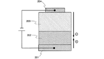
ここで、特許文献1や特許文献2に示された発光素子の動作原理について図2を用いて説明する。
Here, the operation principle of the light-emitting elements disclosed in
図2は、上述した特許文献1や2で述べられている電子注入層を用いた従来の発光素子の基本的な素子構造である。
FIG. 2 shows a basic element structure of a conventional light emitting element using the electron injection layer described in
従来の発光素子(図2)では、順バイアスを印加すると、陽極201から注入された正孔と陰極204から注入された電子が発光物質を含む層202中で再結合し、発光に至る。この時、電子注入層203は、有機化合物に電子供与性の高い金属(アルカリ金属やアルカリ土類金属)をドープした構成である。
In the conventional light-emitting element (FIG. 2), when a forward bias is applied, holes injected from the
この電子注入層203は、電子を流して発光物質を含む層202に電子注入する役割を持つ。しかしながら、有機化合物の電子移動度は正孔移動度に比べて2桁程度小さいため、発光スペクトルを制御するなどの目的で可視光の波長程度(サブミクロンオーダー)の膜厚にすると、駆動電圧が高くなってしまう。
The
以上のような問題に鑑み、本発明では、従来技術のように配位子として機能するような物質を用いる発光素子とは異なる新たな手段によって、容易に膜厚を厚くでき、低駆動電圧で動作できる発光素子を提供することを課題とする。またそれにより、消費電力が低く、なおかつ色純度の高い発光素子を提供することを課題とする。また同時に、消費電力が低く、なおかつ歩留まりの高い発光素子を提供することを課題とする。 In view of the above problems, in the present invention, the film thickness can be easily increased by a new means different from a light emitting element using a substance that functions as a ligand as in the prior art, and at a low driving voltage. It is an object to provide a light-emitting element that can operate. It is another object of the present invention to provide a light-emitting element with low power consumption and high color purity. At the same time, it is an object to provide a light-emitting element with low power consumption and high yield.
本発明者は、鋭意検討を重ねた結果、以下の構成を有する発光素子を提供することにより、課題を解決できることを見出した。 As a result of intensive studies, the present inventor has found that the problem can be solved by providing a light emitting element having the following configuration.
本発明は、陽極と陰極の間に、発光物質を含む第1の層と、n型半導体を含む第2の層と、p型半導体を含む第3の層と、を有し、前記陽極から前記陰極の方向に対し、前記第1の層と前記第2の層と前記第3の層とが順に設けられ、前記第3の層が陰極に接して設けられている発光素子である。 The present invention has a first layer containing a light-emitting substance, a second layer containing an n-type semiconductor, and a third layer containing a p-type semiconductor between the anode and the cathode, In the light-emitting element, the first layer, the second layer, and the third layer are sequentially provided in the direction of the cathode, and the third layer is provided in contact with the cathode.
ここで、n型半導体は、金属酸化物であることが好ましく、特に、酸化亜鉛、酸化錫、および酸化チタンからなる群より選ばれるいずれかの一または二以上の化合物であることが好ましい。また、p型半導体は金属酸化物であることが好ましく、特に、酸化バナジウム、酸化クロム、酸化モリブデン、酸化コバルト、および酸化ニッケルからなる群より選ばれるいずれか一または二以上の化合物であることが好ましい。 Here, the n-type semiconductor is preferably a metal oxide, and particularly preferably one or more compounds selected from the group consisting of zinc oxide, tin oxide, and titanium oxide. Further, the p-type semiconductor is preferably a metal oxide, and in particular, one or more compounds selected from the group consisting of vanadium oxide, chromium oxide, molybdenum oxide, cobalt oxide, and nickel oxide. preferable.
本発明は、陽極と陰極との間に、発光物質を含む第1の層と、有機化合物および電子供与性を示す物質を含む第2の層と、p型半導体を含む第3の層と、を有し、陽極から陰極の方向に対し、第1の層と第2の層と第3の層とが順に設けられ、第3の層が陰極に接するように設けられている発光素子である。 The present invention includes a first layer containing a light emitting substance between an anode and a cathode, a second layer containing an organic compound and a substance exhibiting an electron donating property, a third layer containing a p-type semiconductor, A light-emitting element in which a first layer, a second layer, and a third layer are provided in this order in the direction from the anode to the cathode, and the third layer is in contact with the cathode .
ここで、p型半導体は、金属酸化物であることが好ましく、特に、酸化バナジウム、酸化クロム、酸化モリブデン、酸化コバルト、および酸化ニッケルからなる群より選ばれるいずれか一または二以上の化合物であることが好ましい。また、第2の層の有機化合物は、電子輸送性を示す有機化合物であることが好ましく、特に、π共役骨格を含む配位子を有する金属錯体が好ましい。また、電子供与性を示す物質はアルカリ金属またはアルカリ土類金属または希土類金属であることが好ましい。 Here, the p-type semiconductor is preferably a metal oxide, in particular, one or more compounds selected from the group consisting of vanadium oxide, chromium oxide, molybdenum oxide, cobalt oxide, and nickel oxide. It is preferable. In addition, the organic compound in the second layer is preferably an organic compound exhibiting electron transport properties, and in particular, a metal complex having a ligand including a π-conjugated skeleton is preferable. The substance exhibiting an electron donating property is preferably an alkali metal, an alkaline earth metal, or a rare earth metal.
本発明は、陽極と陰極との間に、発光物質を含む第1の層と、n型半導体を含む第2の層と、有機化合物および電子受容性を示す物質を含む第3の層と、を有し、陽極から陰極の方向に対し、第1の層と第2の層と第3の層とが順に設けられ、第3の層が陰極に接するように設けられている発光素子である。 The present invention includes a first layer containing a light-emitting substance, a second layer containing an n-type semiconductor, a third layer containing an organic compound and a substance exhibiting electron acceptability between an anode and a cathode, A light-emitting element in which a first layer, a second layer, and a third layer are provided in this order in the direction from the anode to the cathode, and the third layer is in contact with the cathode .
ここで、n型半導体は、金属酸化物であることが好ましく、特に、酸化亜鉛、酸化錫、および酸化チタンからなる群より選ばれるいずれか一または二以上の化合物であることが好ましい。また、第3の層の有機化合物は、正孔輸送性の有機化合物であることが好ましく、特に芳香族アミン骨格を有する有機化合物であることが好ましい。また、電子受容性を示す物質は、金属酸化物であることが好ましい。 Here, the n-type semiconductor is preferably a metal oxide, and particularly preferably any one or two or more compounds selected from the group consisting of zinc oxide, tin oxide, and titanium oxide. The organic compound in the third layer is preferably a hole-transporting organic compound, and particularly preferably an organic compound having an aromatic amine skeleton. Further, the substance exhibiting electron accepting properties is preferably a metal oxide.
本発明は、陽極と陰極との間に、発光物質を含む第1の層と、第1の有機化合物および電子供与性を示す物質を含む第2の層と、第2の有機化合物および電子受容性を示す物質を含む第3の層と、を有し、陽極から陰極の方向に対し、第1の層と第2の層と第3の層とが順に設けられ、第3の層が陰極に接するように設けられている発光素子である。 The present invention includes a first layer containing a light-emitting substance, a second layer containing a first organic compound and a substance exhibiting electron donating properties, a second organic compound, and an electron accepting layer between an anode and a cathode. A third layer including a substance exhibiting a property, wherein the first layer, the second layer, and the third layer are sequentially provided in a direction from the anode to the cathode, and the third layer is a cathode. It is a light emitting element provided so that it may touch.
ここで、第1の有機化合物は電子輸送性を示す有機化合物であることが好ましく、特に、π共役骨格を含む配位子を有する金属錯体であることが好ましい。また、電子供与性を示す物質は、アルカリ金属またはアルカリ土類金属または希土類金属であることが好ましい。また、第2の有機化合物は、正孔輸送性の有機化合物であることが好ましく、特に、芳香族アミン骨格を有する有機化合物であることが好ましい。また、電子受容性を示す物質は、金属酸化物であることが好ましい。 Here, the first organic compound is preferably an organic compound exhibiting electron transport properties, and particularly preferably a metal complex having a ligand including a π-conjugated skeleton. The substance exhibiting electron donating properties is preferably an alkali metal, an alkaline earth metal, or a rare earth metal. The second organic compound is preferably a hole-transporting organic compound, and particularly preferably an organic compound having an aromatic amine skeleton. Further, the substance exhibiting electron accepting properties is preferably a metal oxide.
本発明は、陽極と陰極との間に、発光物質を含む第1の層と、有機化合物および金属を含む第2の層と、金属酸化物からなる第3の層と、を有し、陽極から陰極の方向に対し、第1の層と第2の層と第3の層とが順に設けられ、第3の層が陰極に接するように設けられている発光素子である。あるいはまた、陽極と陰極との間に、発光物質を含む第1の層と、有機化合物および金属を含む第2の層と、第2の層に含まれる有機化合物と異なる有機化合物および金属酸化物を含む第3の層と、を有し、陽極から陰極の方向に対し、第1の層と第2の層と第3の層とが順に設けられ、第3の層が陰極に接するように設けられている発光素子である。 The present invention has a first layer containing a luminescent material, a second layer containing an organic compound and a metal, and a third layer made of a metal oxide between the anode and the cathode, and the anode A light-emitting element in which a first layer, a second layer, and a third layer are provided in this order in the direction from to the cathode, and the third layer is in contact with the cathode. Alternatively, a first layer containing a light-emitting substance, a second layer containing an organic compound and a metal, and an organic compound and metal oxide different from the organic compound contained in the second layer are provided between the anode and the cathode. The first layer, the second layer, and the third layer are provided in this order in the direction from the anode to the cathode, and the third layer is in contact with the cathode. It is the light emitting element provided.
ここで、第2の層に含まれる有機化合物は、電子輸送性の有機化合物であることが好ましく、特に、π共役骨格を含む配位子を有する金属錯体であることが好ましい。また、第3の層に含まれる第2の有機化合物は、正孔輸送性の有機化合物が好ましく、特に、芳香族アミン骨格を有する有機化合物であることが好ましい。また、金属は、アルカリ金属またはアルカリ土類金属または希土類金属であることが好ましい。また、金属酸化物は、酸化バナジウム、酸化クロム、酸化モリブデン、酸化コバルト、および酸化ニッケルからなる群より選ばれるいずれか一または二以上の化合物であることが好ましい。 Here, the organic compound contained in the second layer is preferably an electron-transporting organic compound, and particularly preferably a metal complex having a ligand containing a π-conjugated skeleton. The second organic compound contained in the third layer is preferably a hole-transporting organic compound, and particularly preferably an organic compound having an aromatic amine skeleton. The metal is preferably an alkali metal, an alkaline earth metal or a rare earth metal. The metal oxide is preferably one or more compounds selected from the group consisting of vanadium oxide, chromium oxide, molybdenum oxide, cobalt oxide, and nickel oxide.
なお、本発明の発光素子では、陰極の形成にスパッタリング法を用いた場合であっても、スパッタリングによる発光素子の損傷が少なく良好な特性を示す発光素子を得ることができる。このため、主にスパッタリング法によって形成されるインジウム錫酸化物(ITO:indium Tin Oxide)等の可視光を透過できる導電物を用いて陰極を形成することができる。このような、可視光を透過できる導電物から成る透明電極を用いた場合、陰極側からも発光を取り出すことのできる発光素子を得ることができる。 Note that in the light-emitting element of the present invention, even when a sputtering method is used for forming the cathode, a light-emitting element exhibiting favorable characteristics with little damage to the light-emitting element due to sputtering can be obtained. Therefore, the cathode can be formed using a conductive material that can transmit visible light, such as indium tin oxide (ITO) formed mainly by a sputtering method. When such a transparent electrode made of a conductive material that can transmit visible light is used, a light-emitting element that can emit light from the cathode side can be obtained.
本発明によって、従来技術のように配位子として機能するような物質を用いる発光素子とは異なる新たな手段によって、容易に膜厚を厚くでき、低駆動電圧で動作できる発光素子を得ることができる。またそれにより、消費電力が低く、なおかつ色純度の高い発光素子を得ることができる。また同時に、消費電力が低く、なおかつ歩留まりの高い発光素子を得ることができる。 According to the present invention, a light-emitting element that can be easily increased in thickness and operated at a low driving voltage can be obtained by a new means different from a light-emitting element using a substance that functions as a ligand as in the prior art. it can. Accordingly, a light-emitting element with low power consumption and high color purity can be obtained. At the same time, a light-emitting element with low power consumption and high yield can be obtained.
さらに、前記発光素子を用いて発光装置を作製することにより、色純度が高く歩留まりも良好で、消費電力の低い発光装置を提供することができる。 Further, by manufacturing a light-emitting device using the light-emitting element, a light-emitting device with high color purity, high yield, and low power consumption can be provided.
以下では、本発明の実施形態について、動作原理および具体的な構成例を挙げて詳細に説明する。 Hereinafter, embodiments of the present invention will be described in detail with reference to an operation principle and a specific configuration example.
まず、本発明の発光素子の動作原理について、図1を用いて説明する。図1は本発明の発光素子の基本的な素子構造である。 First, the operation principle of the light-emitting element of the present invention will be described with reference to FIG. FIG. 1 shows a basic element structure of a light emitting element of the present invention.
本発明の発光素子は(図1)は、陽極101と陰極105との間に、第1の層102、第2の層103、第3の層104が、陽極101から陰極105の方向に対して順に設けられた構成となっている。なお、本発明における陽極とは、ホールを注入する電極のことをさす。また、本発明における陰極とは、電子を注入する電極として作用してもよいし、ホールを受け取る電極として作用してもよい。
In the light-emitting element of the present invention (FIG. 1), the
第2の層103は、電子を生成し且つ電子を輸送する層であり、n型半導体若しくはそれを含む混合物、又はキャリア輸送性を有する有機化合物と電子供与性の高い物質との混合物から成る。また、第3の層104は、正孔を生成し且つ正孔を輸送する層であり、p型半導体若しくはそれを含む混合物、又はキャリア輸送性を有する有機化合物と電子受容性の高い物質との混合物から成る。さらに、第1の層102は、発光物質を含む層であり、単層または複数の層から成る。
The
なお、第1の層102、第2の層103、第3の層104は、第1の層102において発光領域が形成されるように、各層の膜厚および各層を構成する物質を選んで積層されている。
Note that the
このような構成の発光素子に順バイアスを印加すると、図1に示す通り、第2の層103と第3の層104との界面近傍から、電子と正孔がそれぞれ逆方向に流れ出す。このようにして発生したキャリアのうち、電子の方は陽極101から注入された正孔と再結合し、第1の層102中にて発光に至る。一方、正孔はそのまま陰極105の方へ抜けていくことになる。なおこの時、第2の層103と第3の層104に着目すると、p−n接合に対して逆バイアスが印加されている状態であり、発生するキャリアの量は際だって多いものではないが、発光素子を駆動するには十分な量である。
When a forward bias is applied to the light-emitting element having such a structure, electrons and holes flow out in opposite directions from the vicinity of the interface between the
以上のような、本発明の発光素子では、正孔を発生し、その正孔を移動することのできる第3の層の膜厚を厚くすることで、光学距離を調節できる。この点で、BCPを含んだ電子注入層203、つまり電子を発生し、その電子を輸送する層の膜厚を厚くすることで光学距離を調節している従来型の発光素子(図2)と異なる。
In the light-emitting element of the present invention as described above, the optical distance can be adjusted by increasing the thickness of the third layer that generates holes and can move the holes. In this respect, a conventional light emitting device (FIG. 2) in which the optical distance is adjusted by increasing the thickness of the
通常、正孔輸送材料として用いられている有機化合物の正孔移動度は、電子輸送材料として用いられている有機化合物の電子移動度よりも高移動度である。従って、本発明のように、正孔を移動することのできる層(第3の層)を厚くすることによって、光学距離を調整した方が、膜厚増加に伴う駆動電圧の増加を抑制できる。 Usually, the hole mobility of the organic compound used as the hole transport material is higher than the electron mobility of the organic compound used as the electron transport material. Therefore, as in the present invention, by increasing the optical distance by increasing the thickness of the layer that can move holes (third layer), an increase in driving voltage accompanying an increase in film thickness can be suppressed.
以下、本発明の一態様について図面を参照しながら説明する。但し、本発明は多くの異なる態様で実施することが可能であり、本発明の趣旨及びその範囲から 逸脱することなくその形態及び詳細を様々に変更し得ることは当業者であれば容易に理解される。従って、本実施の形態の記載内容に限定して解釈されるものではない。 Hereinafter, one embodiment of the present invention will be described with reference to the drawings. However, the present invention can be implemented in many different modes, and those skilled in the art can easily understand that the modes and details can be variously changed without departing from the spirit and scope of the present invention. Is done. Therefore, the present invention is not construed as being limited to the description of this embodiment mode.
(実施の形態1)
本実施の形態1では、本発明の発光素子について図3を用いて説明する。
(Embodiment 1)
In
図3では、基板300上に陽極301が形成され、陽極301上に発光物質が含まれる第1の層302が形成され、第1の層302上に第2の層303が形成され、第2の層303上に第3の層304が形成され、その上に陰極305が形成された構造を有する。
In FIG. 3, an anode 301 is formed over a
なお、ここで基板300に用いる材料としては、従来の発光素子に用いられているものであれば良く、例えば、ガラス、石英、透明プラスチック、可撓性を有する基板などからなるものを用いることができる。
Note that the material used for the
陽極301として用いることのできる陽極材料としては、仕事関数の大きい(仕事関数4.0eV以上)金属、合金、電気伝導性化合物、およびこれらの混合物などを用いることが好ましい。なお、陽極材料の具体例としては、ITO(indium tin oxide)、珪素を含有するITO、酸化インジウムに2〜20[%]の酸化亜鉛(ZnO)を混合したIZO(indium zinc oxide)の他、金(Au)、白金(Pt)、ニッケル(Ni)、タングステン(W)、クロム(Cr)、モリブデン(Mo)、鉄(Fe)、コバルト(Co)、銅(Cu)、パラジウム(Pd)、または金属材料の窒化物(TiN)等を用いることができる。 As an anode material that can be used as the anode 301, it is preferable to use a metal, an alloy, an electrically conductive compound, a mixture thereof, or the like having a large work function (work function of 4.0 eV or more). Specific examples of the anode material include ITO (indium tin oxide), ITO containing silicon, IZO (indium zinc oxide) in which 2 to 20% zinc oxide (ZnO) is mixed with indium oxide, Gold (Au), platinum (Pt), nickel (Ni), tungsten (W), chromium (Cr), molybdenum (Mo), iron (Fe), cobalt (Co), copper (Cu), palladium (Pd), Alternatively, a nitride of metal material (TiN) or the like can be used.
一方、陰極305の形成に用いられる陰極材料としては、仕事関数の小さい(仕事関数3.8eV以下)金属、合金、電気伝導性化合物、およびこれらの混合物などを用いることが好ましい。なお、陰極材料の具体例としては、元素周期律の1族または2族に属する元素、すなわちLiやCs等のアルカリ金属、およびMg、Ca、Sr等のアルカリ土類金属、およびこれらを含む合金(Mg:Ag、Al:Li)や化合物(LiF、CsF、CaF2)の他、希土類金属を含む遷移金属を用いて形成することができるが、Al、Ag、ITO等の金属(合金を含む)との積層により形成することもできる。
On the other hand, as a cathode material used for forming the cathode 305, it is preferable to use a metal, an alloy, an electrically conductive compound, a mixture thereof, or the like having a low work function (work function of 3.8 eV or less). Specific examples of the cathode material include elements belonging to
なお、上述した陽極材料及び陰極材料は、蒸着法、スパッタリング法等により薄膜を形成することにより、それぞれ陽極301及び陰極305を形成する。膜厚は、10〜500nmとするのが好ましい。最後にSiN等の無機材料やテフロン(登録商標)、スチレンポリマー等の有機材料からなる保護層(バリア層)を形成してもよい。バリア層は、透明であっても不透明であってもよく、上記無機材料または有機材料は、蒸着法、スパッタリング法等により形成する。 Note that the anode material and the cathode material described above form the anode 301 and the cathode 305 by forming a thin film by a vapor deposition method, a sputtering method, or the like, respectively. The film thickness is preferably 10 to 500 nm. Finally, a protective layer (barrier layer) made of an inorganic material such as SiN or an organic material such as Teflon (registered trademark) or styrene polymer may be formed. The barrier layer may be transparent or opaque, and the inorganic material or organic material is formed by vapor deposition, sputtering, or the like.
さらに、発光素子の有機層や電極の酸化や湿気から防ぐためにSrOxやSiOx等の乾燥剤を電子ビーム照射法、蒸着法、スパッタリング法、ゾル・ゲル法等により形成してもよい。 Further, a desiccant such as SrOx or SiOx may be formed by an electron beam irradiation method, a vapor deposition method, a sputtering method, a sol-gel method or the like in order to prevent oxidation or moisture of the organic layer or electrode of the light emitting element.
また、本発明の発光素子において、第1の層である発光物質を含む層におけるキャリアの再結合により生じる光は、図3に示すとおり、陽極301または陰極305の一方、または両方から外部に出射される構成となる(図中の矢印が発光方向である)。すなわち、陽極301から光を出射させる場合(図3(A))には、陽極301を透光性の材料で形成することとし、陰極305側から光を出射させる場合(図3(B))には、陰極305を透光性の材料で形成することとし、陽極301および陰極305の両側から光を出射させる場合(図3(C))には、陽極301と陰極305を透光性の材料で形成する。 In the light-emitting element of the present invention, light generated by carrier recombination in the first layer containing a light-emitting substance is emitted to the outside from one or both of the anode 301 and the cathode 305 as shown in FIG. (The arrow in the figure is the light emission direction). That is, when light is emitted from the anode 301 (FIG. 3A), the anode 301 is formed of a light-transmitting material and light is emitted from the cathode 305 side (FIG. 3B). In the case where the cathode 305 is formed of a light-transmitting material and light is emitted from both sides of the anode 301 and the cathode 305 (FIG. 3C), the anode 301 and the cathode 305 are made of a light-transmitting material. Form with material.
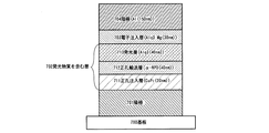
また、第1の層302は複数の層を積層することにより形成されるが、本実施の形態1では、第4の層311、第5の層312、第6の層313を積層することにより形成される。なお、第4の層311は正孔注入性材料を含む正孔注入層であり、第5の層312は正孔輸送性材料を含む正孔輸送層である。第6の層313は、発光物質を含み、電界を印加したときに発光領域が形成される発光層である。
The first layer 302 is formed by stacking a plurality of layers. In
また、第1の層である発光物質を含む層には公知の材料を用いることができ、低分子系材料および高分子系材料のいずれを用いることもできる。 In addition, a known material can be used for the first layer containing a light-emitting substance, and either a low molecular material or a high molecular material can be used.
第4の層311を形成する正孔注入性材料としては、フタロシアニン系の化合物が有効である。例えば、フタロシアニン(略称:H2−Pcと示す)、銅フタロシアニン(略称:Cu−Pcと示す)等を用いることができる。
As the hole injecting material for forming the
第5の層312を形成する正孔輸送性材料としては、芳香族アミン系(すなわち、ベンゼン環−窒素の結合を有するもの)の化合物が好適である。広く用いられている材料として、例えば、4,4’−ビス[N−(3−メチルフェニル)−N−フェニル−アミノ]−ビフェニル(略称:TPD)の他、その誘導体である4,4’−ビス[N−(1−ナフチル)−N−フェニル−アミノ]−ビフェニル(略称:α−NPD)、あるいは4,4’,4’’−トリス(N,N−ジフェニル−アミノ)−トリフェニルアミン(略称:TDATA)、4,4’,4’’−トリス[N−(3−メチルフェニル)−N−フェニル−アミノ]−トリフェニルアミン(略称:MTDATA)などのスターバースト型芳香族アミン化合物が挙げられる。また、酸化モリブデン等の導電性無機化合物を単独、又は上記有機化合物と混合した複合材料等も用いることができる。
As the hole-transporting material for forming the
第6の層313に含まれる発光物質としては、例えば、キナクリドン、クマリン、ルブレン、スチリル系色素、テトラフェニルブタジエン、アントラセン、ペリレン、コロネン、12―フタロペリノン誘導体などの有機化合物の他、トリス(8−キノリノラト)アルミニウム(以下、Alq3と示す)等の金属錯体が挙げられる。
Examples of the light-emitting substance contained in the
第2の層303は、酸化亜鉛、酸化錫、酸化チタン、硫化亜鉛、セレン化亜鉛、テルル化亜鉛などのn型半導体からなる構成であるか、またはそれらn型半導体を含む構成であればよい。あるいはまた、有機化合物に電子供与性を示す物質をドープした構成であってもよい。この時の有機化合物としては電子輸送性材料が好ましく、2−(4−ビフェニリル)−5−(4−tert−ブチルフェニル)−1,3,4−オキサジアゾール(略称:PBD)や、先に述べたOXD−7、TAZ、p−EtTAZ、BPhen、BCPが挙げら、この他に従来では駆動電圧の上昇が見られたAlq3、トリス(5−メチル−8−キノリノラト)アルミニウム(略称:Almq3)、ビス(10−ヒドロキシベンゾ[h]−キノリナト)ベリリウム略称:BeBq2)などのキノリン骨格またはベンゾキノリン骨格を有する金属錯体や、ビス(2−メチル−8−キノリノラト)−4−フェニルフェノラト−アルミニウム(略称:BAlq)が挙げられる。一方、電子供与性を示す物質としては、LiやCs等のアルカリ金属、およびMg、Ca、Sr等のアルカリ土類金属、またはEr、Yb等の希土類金属が挙げられる。この他に、例えばAlq3に対して電子供与性を示すテトラチアフルバレンやテトラメチルチアフルバレンのような有機化合物であってもよい。 The second layer 303 may be configured by an n-type semiconductor such as zinc oxide, tin oxide, titanium oxide, zinc sulfide, zinc selenide, zinc telluride, or the like, as long as it includes the n-type semiconductor. . Alternatively, the organic compound may be doped with a substance exhibiting electron donating properties. The organic compound at this time is preferably an electron transporting material, such as 2- (4-biphenylyl) -5- (4-tert-butylphenyl) -1,3,4-oxadiazole (abbreviation: PBD), OXD-7, TAZ, p-EtTAZ, BPhen, and BCP mentioned above, Alq 3 , tris (5-methyl-8-quinolinolato) aluminum (abbreviation: Almq 3 ), bis (10-hydroxybenzo [h] -quinolinato) beryllium abbreviation: BeBq 2 ) and other metal complexes having a quinoline skeleton or a benzoquinoline skeleton, and bis (2-methyl-8-quinolinolato) -4-phenyl And phenolate-aluminum (abbreviation: BAlq). On the other hand, examples of the substance exhibiting an electron donating property include alkali metals such as Li and Cs, alkaline earth metals such as Mg, Ca, and Sr, and rare earth metals such as Er and Yb. In addition, for example, an organic compound such as tetrathiafulvalene or tetramethylthiafulvalene that exhibits an electron donating property to Alq 3 may be used.
第3の層304は、酸化バナジウム、酸化クロム、酸化モリブデン、酸化コバルト、酸化ニッケルなどのp型半導体からなる構成であるか、またはそれらp型半導体を含む構成であればよい。あるいはまた、有機化合物に電子受容性を示す物質をドープした構成であってもよい。この時の有機化合物としては正孔輸送性材料が好ましく、芳香族アミン系の化合物が好適である。例えば、TPDの他、その誘導体であるα−NPD、あるいはTDATA、MTDATAなどのスターバースト型芳香族アミン化合物が挙げられる。一方、電子受容性を示す物質としては、例えばα−NPDに対して電子受容性を示す酸化モリブデンや酸化バナジウムのような金属酸化物が挙げられる。また、α−NPDに対して電子受容性を示すテトラシアノキノジメタン(略称:TCNQ)や2,3―ジシアノナフトキノン(略称:DCNNQ)のような有機化合物であってもよい。 The third layer 304 may have a structure including a p-type semiconductor such as vanadium oxide, chromium oxide, molybdenum oxide, cobalt oxide, or nickel oxide, or any structure including the p-type semiconductor. Alternatively, a configuration in which an organic compound is doped with a substance exhibiting electron accepting properties may be used. As the organic compound at this time, a hole transporting material is preferable, and an aromatic amine compound is preferable. For example, in addition to TPD, α-NPD which is a derivative thereof, or starburst type aromatic amine compounds such as TDATA and MTDATA can be mentioned. On the other hand, examples of the substance that exhibits electron acceptability include metal oxides such as molybdenum oxide and vanadium oxide that exhibit electron acceptability with respect to α-NPD. Alternatively, an organic compound such as tetracyanoquinodimethane (abbreviation: TCNQ) or 2,3-dicyanonaphthoquinone (abbreviation: DCNNQ) which exhibits an electron accepting property with respect to α-NPD may be used.
以上により、本発明の発光素子を形成することができる。なお、本形態では、図示していないが、第1の層302の一部に、第2の層303と接するように電子輸送性に優れた材料から成る層を設けた構造にしてもよい。電子輸送性に優れた材料の具体例としては、例えばトリス(8−キノリノラト)アルミニウム(略称:Alq3)、トリス(5−メチル−8−キノリノラト)アルミニウム(略称:Almq3)、ビス(10−ヒドロキシベンゾ[h]−キノリナト)ベリリウム(略称:BeBq2)、ビス(2−メチル−8−キノリノラト)−4−フェニルフェノラト−アルミニウム(略称:BAlq)など、キノリン骨格またはベンゾキノリン骨格を有する金属錯体等からなる層である。また、この他ビス[2−(2−ヒドロキシフェニル)−ベンゾオキサゾラト]亜鉛(略称:Zn(BOX)2)、ビス[2−(2−ヒドロキシフェニル)−ベンゾチアゾラト]亜鉛(略称:Zn(BTZ)2)などのオキサゾール系、チアゾール系配位子を有する金属錯体なども用いることができる。さらに、金属錯体以外にも、2−(4−ビフェニリル)−5−(4−tert−ブチルフェニル)−1,3,4−オキサジアゾール(略称:PBD)や、1,3−ビス[5−(p−tert−ブチルフェニル)−1,3,4−オキサジアゾール−2−イル]ベンゼン(略称:OXD−7)、3−(4−tert−ブチルフェニル)−4−フェニル−5−(4−ビフェニリル)−1,2,4−トリアゾール(略称:TAZ)、3−(4−tert−ブチルフェニル)−4−(4−エチルフェニル)−5−(4−ビフェニリル)−1,2,4−トリアゾール(略称:p−EtTAZ)、バソフェナントロリン(略称:BPhen)、バソキュプロイン(略称:BCP)なども用いることができる Through the above steps, the light-emitting element of the present invention can be formed. Although not illustrated in this embodiment mode, a structure in which a layer made of a material having excellent electron transport properties is provided so as to be in contact with the second layer 303 may be provided in part of the first layer 302. Specific examples of a material excellent in electron transporting property include, for example, tris (8-quinolinolato) aluminum (abbreviation: Alq 3 ), tris (5-methyl-8-quinolinolato) aluminum (abbreviation: Almq 3 ), bis (10- Hydroxybenzo [h] -quinolinato) beryllium (abbreviation: BeBq 2 ), bis (2-methyl-8-quinolinolato) -4-phenylphenolato-aluminum (abbreviation: BAlq), and other metals having a quinoline skeleton or a benzoquinoline skeleton It is a layer made of a complex or the like. In addition, bis [2- (2-hydroxyphenyl) -benzoxazolate] zinc (abbreviation: Zn (BOX) 2 ), bis [2- (2-hydroxyphenyl) -benzothiazolate] zinc (abbreviation: Zn ( Metal complexes having an oxazole or thiazole ligand such as BTZ) 2 ) can also be used. In addition to metal complexes, 2- (4-biphenylyl) -5- (4-tert-butylphenyl) -1,3,4-oxadiazole (abbreviation: PBD), 1,3-bis [5 -(P-tert-butylphenyl) -1,3,4-oxadiazol-2-yl] benzene (abbreviation: OXD-7), 3- (4-tert-butylphenyl) -4-phenyl-5 (4-Biphenylyl) -1,2,4-triazole (abbreviation: TAZ), 3- (4-tert-butylphenyl) -4- (4-ethylphenyl) -5- (4-biphenylyl) -1,2 , 4-triazole (abbreviation: p-EtTAZ), bathophenanthroline (abbreviation: BPhen), bathocuproine (abbreviation: BCP), and the like can also be used.
上記の本発明の発光素子において、可視光を透過する導電物で陰極を形成した場合、図3(B)のように、陰極側から発光を取り出すことができる。また、可視光を透過する導電物で陽極を形成した場合、図3(A)のように、陽極側から発光を取り出すことができる。さらに、陰極及び陽極をいずれも可視光を透過する導電物で形成した場合は、図3(C)のように、両側から発光を取り出すことができる。 In the light-emitting element of the present invention, when the cathode is formed using a conductive material that transmits visible light, light emission can be extracted from the cathode side as illustrated in FIG. When the anode is formed using a conductive material that transmits visible light, light emission can be extracted from the anode side as illustrated in FIG. Further, in the case where both the cathode and the anode are formed using a conductive material that transmits visible light, light emission can be extracted from both sides as illustrated in FIG.
可視光を透過でき、また導電性も比較的高い導電物としては、先に記載したような、ITOやIZO等が挙げられる。これらは仕事関数が高いため、通常、陰極を形成する材料としては不適とされている。 Examples of the conductive material that can transmit visible light and have relatively high conductivity include ITO and IZO as described above. Since these have a high work function, they are usually not suitable as materials for forming a cathode.
しかし、本発明の発光素子では、正孔を生成し且つ正孔を輸送する層及び電子を生成し電子を輸送する層を設けた構成となっていることによって、ITOやIZOのような仕事関数の高い材料を用いても、駆動電圧が上がることがない。従って、本発明の発光素子では、陰極を形成するための材料として、ITOやIZO等を用いることができる。 However, in the light emitting device of the present invention, a work function such as ITO or IZO is provided by providing a layer that generates holes and transports holes and a layer that generates electrons and transports electrons. Even if a high material is used, the driving voltage does not increase. Therefore, in the light emitting element of the present invention, ITO, IZO, or the like can be used as a material for forming the cathode.
さらに、本発明の発光素子では、陰極の形成にスパッタリング法を用いた場合であっても、スパッタリングによる発光素子の損傷が少なく良好な特性を示す発光素子を得ることができる。このことは、主にスパッタリング法によって形成されるITO等の可視光を透過できる導電物を用いて陰極を形成する際に有利である。 Furthermore, in the light-emitting element of the present invention, even when a sputtering method is used for forming the cathode, a light-emitting element that exhibits favorable characteristics with little damage to the light-emitting element due to sputtering can be obtained. This is advantageous when the cathode is formed using a conductive material that can transmit visible light, such as ITO, mainly formed by sputtering.
(実施の形態2)
本実施の形態2では、本発明の発光素子の構成について図4を用いて説明する。
(Embodiment 2)
In Embodiment Mode 2, the structure of the light-emitting element of the present invention will be described with reference to FIG.
なお、基板400、陽極401、第1の層402、第2の層403、第3の層404、陰極405については、実施の形態1と同様の材料を用いて、同様にして形成することができるため説明を省略する。
Note that the
また、図4では、基板400上に陰極405が形成され、陰極405上に第3の層404が形成され、第3の層404上に第2の層403が形成され、第2の層403上に発光物質を含む第1の層402が形成され、その上に陽極401が形成された構造を有する。
In FIG. 4, the cathode 405 is formed over the
また、本発明の発光素子において、第1の層である発光物質を含む層におけるキャリアの再結合により生じる光は、陽極401または陰極405の一方、または両方から外部に出射される構成となる。すなわち、陽極401から光を出射させる場合(図4(A))には、陽極401を透光性の材料で形成することとし、陰極405側から光を出射させる場合(図4(B))には、陰極405を透光性の材料で形成することとし、陽極401および陰極405の両側から光を出射させる場合(図4(C))には、陽極401と陰極405を透光性の材料で形成する。 In the light-emitting element of the present invention, light generated by carrier recombination in the first layer containing a light-emitting substance is emitted to the outside from one or both of the anode 401 and the cathode 405. That is, when light is emitted from the anode 401 (FIG. 4A), the anode 401 is formed of a light-transmitting material, and light is emitted from the cathode 405 side (FIG. 4B). In the case where the cathode 405 is formed of a light-transmitting material and light is emitted from both sides of the anode 401 and the cathode 405 (FIG. 4C), the anode 401 and the cathode 405 are made transparent. Form with material.
以上により、本発明の発光素子を作製することができる。 Through the above steps, the light-emitting element of the present invention can be manufactured.
上記の本発明の発光素子において、可視光を透過する導電物で陽極を形成した場合、図4(A)のように、陽極側から発光を取り出すことができる。また、可視光を透過する導電物で陰極を形成した場合、図4(B)のように、陰極側から発光を取り出すことができる。さらに、陰極及び陽極をいずれも可視光を透過する導電物で形成した場合は、図4(C)のように、両側から発光を取り出すことができる。 In the light-emitting element of the present invention, when the anode is formed using a conductive material that transmits visible light, light emission can be extracted from the anode side as illustrated in FIG. Further, in the case where the cathode is formed using a conductive material that transmits visible light, light emission can be extracted from the cathode side as illustrated in FIG. Further, in the case where both the cathode and the anode are formed using a conductive material that transmits visible light, light emission can be extracted from both sides as illustrated in FIG.
なお、実施の形態2でも述べたように、可視光を透過でき、また導電性も比較的高い導電物としては、先に記載したような、ITOやIZO等が挙げられる。これらは仕事関数が高いため、通常、陰極を形成する材料としては不適とされている。 As described in the second embodiment, examples of the conductive material that can transmit visible light and have relatively high conductivity include ITO and IZO as described above. Since these have a high work function, they are usually not suitable as materials for forming a cathode.
しかし、本発明の発光素子では、正孔を生成し且つ正孔を輸送する層及び電子を生成し電子を輸送する層を設けた構成となっていることによって、ITOやIZOのような仕事関数の高い材料を用いても、駆動電圧が上がることがない。従って、本発明の発光素子では、陰極を形成するための材料として、ITOやIZO等を用いることができる。 However, in the light emitting device of the present invention, a work function such as ITO or IZO is provided by providing a layer that generates holes and transports holes and a layer that generates electrons and transports electrons. Even if a high material is used, the driving voltage does not increase. Therefore, in the light emitting element of the present invention, ITO, IZO, or the like can be used as a material for forming the cathode.
(実施の形態3)
本実施の形態においては、ガラス、石英、金属、バルク半導体、透明プラスチック、可撓性基板などからなる基板500上に発光素子を作製している。一基板上にこのような発光素子を複数作製することで、パッシブ型の発光装置を作製することができる。また、ガラス、石英、透明プラスチック、可撓性基板などからなる基板以外に、例えば図5に示すように、薄膜トランジスタ(TFT)アレイと接する発光素子を作製してもよい。ここでは、511と512をTFTとし、513を本発明の発光素子とする。発光素子513は陽極514、第1の層、第2の層および第3の層を515と、陰極516から成り、配線517を介してTFT511と電気的に接続されている。これにより、TFTによって発光素子の駆動を制御するアクティブマトリクス型の発光装置を作製できる。なお、TFTの構造は、特に限定されない。例えば、スタガ型でもよいし、逆スタガ型でもよい。またTFTを構成している半導体層の結晶性についても特に限定されず、結晶質のものでもよいし非晶質のものでもよい。
(Embodiment 3)
In this embodiment mode, a light-emitting element is manufactured over a
本実施例では、本発明の発光素子の一態様について具体的に例示する。素子構造を図6を用いて説明する。 In this example, one embodiment of the light-emitting element of the present invention is specifically illustrated. The element structure will be described with reference to FIG.
まず、基板600上に発光素子の陽極601が形成される。材料として透明導電膜であるITOを用い、スパッタリング法により110nmの膜厚で形成した。陽極601の形状は2mm角とした。
First, the anode 601 of the light emitting element is formed on the
次に、陽極601上に発光物質を含む第1の層602が形成される。なお、本実施例における発光物質を含む第1の層602は、3つの層、すなわち正孔注入層611、正孔輸送層612、発光層613からなる積層構造を有している。
Next, a first layer 602 including a light emitting substance is formed over the anode 601. Note that the first layer 602 containing a light-emitting substance in this embodiment has a stacked structure including three layers, that is, a
まず、陽極601が形成された基板を真空蒸着装置の基板ホルダーに陽極601が形成された面を下方にして固定し、真空蒸着装置の内部に備えられた蒸発源に銅フタロシアニン(以下、Cu−Pcと示す)を入れ、抵抗加熱法を用いた蒸着法により20nmの膜厚で正孔注入層611を形成した。なお、611を形成する材料としては、公知の正孔注入性材料を用いることができる。
First, the substrate on which the anode 601 is formed is fixed to the substrate holder of the vacuum deposition apparatus with the surface on which the anode 601 is formed facing down, and copper phthalocyanine (hereinafter referred to as Cu--) is attached to the evaporation source provided in the vacuum deposition apparatus. The
次に、正孔輸送性に優れた材料により正孔輸送層612を形成する。612を形成する材料としては、公知の正孔輸送性材料を用いることができるが、本実施例では、α−NPDを用い、同様の方法により40nmの膜厚で形成した。
Next, the
次に、発光層613を形成する。613を形成する材料としては、公知の発光物質を用いることができるが、本実施例では、Alq3を同様の方法により、40nmの膜厚で形成した。ここでは、Alq3が発光物質として作用する。
Next, the
このようにして、3つの層611、612、613を積層して形成したあと、第2の層603が形成される。本実施例では、電子輸送性材料としてAlq3を、Alq3に対して電子供与性を示す物質としてMgを用い、30nmの膜厚で共蒸着法により第2の層603を形成した。Mgの割合は1wt%とした。
In this way, after the three
次に、第3の層604が形成される。本実施例では、正孔輸送性材料としてα−NPDを、α−NPDに対して電子受容性を示す物質として酸化モリブデンを用い、150nmの膜厚で共蒸着法により第3の層を形成した。酸化モリブデンの割合は25wt%とした。なお、酸化モリブデンの原料としては、酸化モリブデン(VI)を用いた。 Next, a third layer 604 is formed. In this example, α-NPD was used as a hole transporting material, molybdenum oxide was used as a substance showing electron accepting property to α-NPD, and the third layer was formed by a co-evaporation method with a thickness of 150 nm. . The proportion of molybdenum oxide was 25 wt%. In addition, molybdenum oxide (VI) was used as a raw material for molybdenum oxide.
次に、陰極605をスパッタリング法または蒸着法により形成する。なお、本実施例では、第3の層604上にアルミニウム(150nm)を蒸着法により形成することにより陰極605を得た。
Next, the
以上のようにして、本発明の発光素子を形成した。得られた素子の輝度−電圧特性を図11に、電流−電圧特性を図12に、電流を1mA流した時の発光スペクトルを図13にそれぞれ示す。 As described above, the light emitting device of the present invention was formed. FIG. 11 shows the luminance-voltage characteristics of the obtained device, FIG. 12 shows the current-voltage characteristics, and FIG. 13 shows the emission spectrum when a current of 1 mA is passed.
形成された発光素子に電圧を印加すると、発光開始電圧(ここでは、輝度が1cd/m2となる時の電圧)は6.0Vであった。また、電流を1mA流した時の輝度は1130cd/m2であった。また、この時のCIE色度座標は(X,Y)=(0.29,0.63)であり、色純度のよい緑色となっていた。 When voltage was applied to the formed light emitting element, the light emission start voltage (here, voltage when the luminance was 1 cd / m 2 ) was 6.0 V. Further, the luminance when a current of 1 mA was passed was 1130 cd / m 2 . Further, the CIE chromaticity coordinates at this time were (X, Y) = (0.29, 0.63), and the color purity was green.
(比較例1)
本比較例1では、本発明の第2の層および第3の層を用いず、代わりに電子注入層703を設けた従来の発光素子について具体的に例示する。素子構造を図7を用いて説明する。電子注入層703としては、実施例1の第2の層603と同様に、電子輸送性材料Alq3に電子供与性を示す物質であるMgを1%ドープした構成を適用した。電子注入層703の膜厚は、実施例1における第2の層と同様、30nmとした。また、他の基板700、陽極701、正孔注入層711と正孔輸送層712と発光層713からなる発光物質を含む層702、陰極704は全て実施例1と同様の構成とした。したがって、実施例1は本比較例1に比べて、第3の層604の膜厚(150nm)だけ厚いことになる。
(Comparative Example 1)
In Comparative Example 1, a conventional light-emitting element in which the second layer and the third layer of the present invention are not used and an electron injection layer 703 is provided instead will be specifically illustrated. The element structure will be described with reference to FIG. As the electron injecting layer 703, similarly to the second layer 603 of Example 1, a configuration in which 1% of Mg, which is an electron-donating substance, was doped into the electron transporting material Alq 3 was applied. The film thickness of the electron injection layer 703 was set to 30 nm, like the second layer in Example 1. The
得られた素子の輝度−電圧特性を図11に、電流−電圧特性を図12に、電流を1mA流した時の発光スペクトルを図13にそれぞれ示す。形成された発光素子に電圧を印加すると、発光開始電圧は5.4Vであった。また、電流を1mA流した時の輝度は1360cd/m2であった。また、この時のCIE色度座標は(X,Y)=(0.34,0.58)であり、色純度が余りよくない黄緑色であった。 FIG. 11 shows the luminance-voltage characteristics of the obtained device, FIG. 12 shows the current-voltage characteristics, and FIG. 13 shows the emission spectrum when a current of 1 mA is passed. When voltage was applied to the formed light emitting device, the light emission starting voltage was 5.4V. Further, the luminance when a current of 1 mA was passed was 1360 cd / m 2 . Further, the CIE chromaticity coordinates at this time were (X, Y) = (0.34, 0.58), and the color was yellow-green with not very good color purity.
以上の結果から、本発明の実施例1は、本比較例1に比べてトータル膜厚が150nmも厚いにもかかわらず、その駆動電圧(6.0V)は本比較例1(5.4V)とほとんど変わらないことがわかった。また、図13中の発光スペクトルを比較すると、実施例1は比較例1の発光スペクトルに比べてスペクトル幅が狭く、このことが色純度の向上に繋がっていると考えられる。 From the above results, Example 1 of the present invention has a driving voltage (6.0 V) of Comparative Example 1 (5.4 V) although the total film thickness is 150 nm thicker than Comparative Example 1. It turned out that there is almost no change. Further, when the emission spectra in FIG. 13 are compared, Example 1 has a narrower spectrum width than the emission spectrum of Comparative Example 1, which is thought to lead to an improvement in color purity.
(比較例2)
本比較例2では、基板800、陽極801、正孔注入層811と正孔輸送層812と発光層813からなる発光物質を含む層802、陰極804は全て実施例1と同様の構成とし、電子注入層803を設けた従来の発光素子について具体的に例示する。素子構造を図8を用いて説明する。ここでは、電子注入層803の構成は比較例1と同様であるが、膜厚を180nmとすることで、トータル膜厚を実施例1と揃えた。
(Comparative Example 2)
In this comparative example 2, the
得られた素子の輝度−電圧特性を図11に、電流−電圧特性を図12に、電流を1mA流した時の発光スペクトルを図13にそれぞれ示す。形成された発光素子に電圧を印加すると、発光開始電圧は14.0Vであった。また、電流を1mA流した時の輝度は1050cd/m2であった。また、この時のCIE色度座標は(X,Y)=(0.25,0.63)であり、色純度の良い緑色であった。 FIG. 11 shows the luminance-voltage characteristics of the obtained device, FIG. 12 shows the current-voltage characteristics, and FIG. 13 shows the emission spectrum when a current of 1 mA is passed. When voltage was applied to the formed light emitting device, the light emission starting voltage was 14.0V. Further, the luminance when a current of 1 mA was passed was 1050 cd / m 2 . Further, the CIE chromaticity coordinates at this time were (X, Y) = (0.25, 0.63), and the color purity was green.
以上の結果から、比較例2の構成では、図13を見てわかるとおりスペクトル幅が狭く、色純度はよいものの、同膜厚である本発明の実施例1に比べて駆動電圧が著しく上昇してしまったことがわかる。 From the above results, in the configuration of Comparative Example 2, the spectral width is narrow and the color purity is good as can be seen from FIG. 13, but the driving voltage is remarkably increased as compared with Example 1 of the present invention having the same film thickness. You can see that
したがって、一対の電極(陽極601および陰極605)の間に、第1の層602と第2の層603と第3の層604とを順に設けるという本発明の構成を実施することで、膜厚を厚くすることで色純度を向上させることができると同時に、膜厚を厚くしても駆動電圧の上昇を抑えることができることがわかった。 Therefore, by implementing the structure of the present invention in which the first layer 602, the second layer 603, and the third layer 604 are sequentially provided between the pair of electrodes (the anode 601 and the cathode 605), the film thickness It has been found that the color purity can be improved by increasing the thickness, and at the same time, the increase in driving voltage can be suppressed even when the thickness is increased.
本実施例2では、本発明の発光素子の一態様について具体的に例示する。素子構造を図14を用いて説明する。 Example 2 specifically illustrates one embodiment of the light-emitting element of the present invention. The element structure will be described with reference to FIG.
まず、基板2400上に発光素子の陽極2401が形成される。材料として透明導電膜であるITOを用い、スパッタリング法により110nmの膜厚で形成した。陽極2401の形状は2mm角とした。
First, the
次に、陽極2401上に発光物質を含む第1の層2402が形成される。なお、本実施例における発光物質を含む第1の層2402は、3つの層、すなわち正孔注入層2411、正孔輸送層2412、発光層2413からなる積層構造を有している。
Next, a
まず、陽極2401が形成された基板を真空蒸着装置の基板ホルダーに陽極2401が形成された面を下方にして固定し、真空蒸着装置の内部に備えられた蒸発源にCu−Pcを入れ、抵抗加熱法を用いた蒸着法により20nmの膜厚で正孔注入層2411を形成した。なお、2411を形成する材料としては、公知の正孔注入性材料を用いることができる。
First, the substrate on which the
次に、正孔輸送性に優れた材料により正孔輸送層2412を形成する。2412を形成する材料としては、公知の正孔輸送性材料を用いることができるが、本実施例では、α−NPDを用い、同様の方法により40nmの膜厚で形成した。
Next, the
次に、発光層2413を形成する。2413には公知の発光物質を用いることができるが、本実施例では、Alq3およびクマリン6を共蒸着することにより、Alq3およびクマリン6からなる層を40nmの膜厚で形成した。ここでは、クマリン6が発光物質として作用する。なお、共蒸着の際には、Alq3とクマリン6の質量比が、Alq3:クマリン6=1:0.003となるように調節した。
Next, the
このようにして、3つの層2411、2412、2413を積層して形成したあと、第2の層2403が形成される。本実施例では、電子輸送性材料としてAlq3を、Alq3に対して電子供与性を示す物質としてLiを用い、30nmの膜厚で共蒸着法により第2の層2403を形成した。Liの割合は1wt%とした。
After the three
次に、第3の層2404が形成される。本実施例では、正孔輸送性材料としてα−NPDを、α−NPDに対して電子受容性を示す物質として酸化モリブデンを用い、180nmの膜厚で共蒸着法により第3の層2404を形成した。酸化モリブデンの割合は25wt%とした。なお、酸化モリブデンの原料としては、酸化モリブデン(VI)を用いた。
Next, a
次に、陰極2405をスパッタリング法または蒸着法により形成する。なお、本実施例では、第3の層2404上にアルミニウム(200nm)を蒸着法により形成することにより陰極2405を得た。
Next, the cathode 2405 is formed by a sputtering method or an evaporation method. Note that in this example, a cathode 2405 was obtained by forming aluminum (200 nm) over the
以上のようにして形成された発光素子に電圧を印加すると、発光開始電圧(ここでは、輝度が1cd/m2となる時の電圧)は3.4Vであった。また、電流を1mA流した時の輝度は2700cd/m2であり、発光スペクトルは図16に示すようにシャープな形状を示した。また、この時のCIE色度座標は(X,Y)=(0.21,0.69)であり、極めて色純度のよい緑色となっていた。 When voltage was applied to the light-emitting element formed as described above, the light emission start voltage (here, voltage when the luminance was 1 cd / m 2 ) was 3.4 V. Further, the luminance when a current of 1 mA was applied was 2700 cd / m 2 , and the emission spectrum showed a sharp shape as shown in FIG. Further, the CIE chromaticity coordinates at this time were (X, Y) = (0.21, 0.69), and the color was very good in green.
(比較例3)
本比較例3では、本発明の第2の層および第3の層を用いず、代わりに電子注入層2503を設けた従来の発光素子について図15を用いて説明する。電子注入層2503としては、実施例2の第2の層2403と同様に、電子輸送性材料Alq3に電子供与性を示す物質であるLiを1wt%ドープした構成を適用した。電子注入層2503の膜厚は、実施例2における第2の層と同様、30nmとした。また、他の基板2500、陽極2501、正孔注入層2511と正孔輸送層2512と発光層2513からなる発光物質を含む層2502、陰極2504は全て実施例2と同様の構成とした。したがって、実施例2は本比較例3に比べて、第3の層2404の膜厚(180nm)だけ厚いことになる。
(Comparative Example 3)
In Comparative Example 3, a conventional light-emitting element in which an
得られた本比較例3の素子に電圧を印加すると、発光開始電圧は3.2Vであった。また、電流を1mA流した時の輝度は3300cd/m2であったが、発光スペクトルは図16に示すようにブロードな形状を示した。また、この時のCIE色度座標は(X,Y)=(0.30,0.64)であり、色純度が余りよくない緑色であった。 When voltage was applied to the obtained device of Comparative Example 3, the light emission starting voltage was 3.2V. Further, the luminance when the current was passed at 1 mA was 3300 cd / m 2 , but the emission spectrum showed a broad shape as shown in FIG. In addition, the CIE chromaticity coordinates at this time were (X, Y) = (0.30, 0.64), and the green color was not so good in color purity.
以上の結果から、本発明の実施例2は、本比較例3に比べてトータル膜厚が180nmも厚いにもかかわらず、その駆動電圧(3.4V)は本比較例3(3.2V)とほとんど変わらないことがわかった。また、図16中の発光スペクトルを比較すると、実施例2は本比較例3の発光スペクトルに比べてスペクトル幅が狭く、このことが色純度の向上に繋がっていると考えられる。 From the above results, Example 2 of the present invention has a driving voltage (3.4 V) of the present comparative example 3 (3.2 V) although the total film thickness is 180 nm thicker than that of the present comparative example 3. It turned out that there is almost no change. Further, when the emission spectra in FIG. 16 are compared, Example 2 has a narrower spectrum width than the emission spectrum of Comparative Example 3, which is thought to lead to an improvement in color purity.
本実施例3では、本発明の発光素子の一態様について例示する。素子構造を図14を用いて説明する。本実施例3では、第3の層2404以外は実施例2と同様にして形成した。また、第3の層2404は、酸化モリブデンのみを260nm蒸着することにより形成した。なお、酸化モリブデンの原料は、酸化モリブデン(VI)を用いた。
In Example 3, one embodiment of the light-emitting element of the present invention is illustrated. The element structure will be described with reference to FIG. In this example 3, a layer other than the
以上のようにして形成された発光素子に電圧を印加すると、発光開始電圧(ここでは、輝度が1cd/m2となる時の電圧)は4.6Vであった。また、電流を1mA流した時の輝度は2800cd/m2であり、発光スペクトルは図17に示すようにシャープな形状を示した。また、この時のCIE色度座標は(X,Y)=(0.23,0.71)であり、極めて色純度のよい緑色となっていた。比較のため、先に述べた比較例3の発光スペクトルも図17中に合わせて載せた。 When voltage was applied to the light-emitting element formed as described above, the light emission start voltage (here, voltage when the luminance was 1 cd / m 2 ) was 4.6 V. Further, the luminance when a current of 1 mA was applied was 2800 cd / m 2 , and the emission spectrum showed a sharp shape as shown in FIG. In addition, the CIE chromaticity coordinates at this time are (X, Y) = (0.23, 0.71), which is green with extremely good color purity. For comparison, the emission spectrum of Comparative Example 3 described above is also shown in FIG.
以上の結果から、本発明の実施例3は、比較例3に比べてトータル膜厚が260nmも厚いにもかかわらず、その駆動電圧(4.6V)は比較例3(3.2V)に比べて顕著な上昇は見られなかった。また、図17中の発光スペクトルを比較すると、実施例3は比較例3の発光スペクトルに比べてスペクトル幅が狭く、このことが色純度の向上に繋がっていると考えられる。 From the above results, Example 3 of the present invention has a driving voltage (4.6 V) that is higher than that of Comparative Example 3 (3.2 V) even though the total film thickness is 260 nm thicker than that of Comparative Example 3. There was no significant increase. Further, when the emission spectra in FIG. 17 are compared, Example 3 has a narrower spectrum width than the emission spectrum of Comparative Example 3, which is thought to lead to an improvement in color purity.
本実施例では、画素部に本発明の発光素子を有する発光装置について図9を用いて説明する。なお、図9(A)は、発光装置を示す上面図、図9(B)は図9(A)をA−A’で切断した断面図である。点線で示された901は駆動回路部(ソース側駆動回路)、902は画素部、903は駆動回路部(ゲート側駆動回路)である。また、904は封止基板、905はシール剤であり、シール剤905で囲まれた内側907は、空間になっている。
In this embodiment, a light-emitting device having the light-emitting element of the present invention in a pixel portion will be described with reference to FIG. 9A is a top view illustrating the light-emitting device, and FIG. 9B is a cross-sectional view taken along line A-A ′ in FIG. 9A. Reference numeral 901 indicated by a dotted line is a drive circuit portion (source side drive circuit), 902 is a pixel portion, and 903 is a drive circuit portion (gate side drive circuit). Reference numeral 904 denotes a sealing substrate,
なお、908はソース側駆動回路901及びゲート側駆動回路903に入力される信号を伝送するための配線であり、外部入力端子となるFPC(フレキシブルプリントサーキット)909からビデオ信号、クロック信号、スタート信号、リセット信号等を受け取る。なお、ここではFPCしか図示されていないが、このFPCにはプリント配線基盤(PWB)が取り付けられていても良い。本明細書における発光装置には、発光装置本体だけでなく、それにFPCもしくはPWBが取り付けられた状態をも含むものとする。 Reference numeral 908 denotes a wiring for transmitting signals input to the source side driver circuit 901 and the gate side driver circuit 903, and a video signal, a clock signal, and a start signal from an FPC (flexible printed circuit) 909 serving as an external input terminal. Receive a reset signal, etc. Although only the FPC is shown here, a printed wiring board (PWB) may be attached to the FPC. The light-emitting device in this specification includes not only a light-emitting device body but also a state in which an FPC or a PWB is attached thereto.
次に、断面構造について図9(B)を用いて説明する。基板910上には駆動回路部及び画素部が形成されているが、ここでは、駆動回路部であるソース側駆動回路901と、画素部902が示されている。
Next, a cross-sectional structure is described with reference to FIG. A driver circuit portion and a pixel portion are formed over the
なお、ソース側駆動回路901はnチャネル型TFT923とpチャネル型TFT924とを組み合わせたCMOS回路が形成される。また、駆動回路を形成するTFTは、公知のCMOS回路、PMOS回路もしくはNMOS回路で形成しても良い。また、本実施例では、基板上に駆動回路を形成したドライバー一体型を示すが、必ずしもその必要はなく、基板上ではなく外部に形成することもできる。
Note that the source side driver circuit 901 is a CMOS circuit in which an n-
また、画素部902はスイッチング用TFT911と、電流制御用TFT912とそのドレインに電気的に接続された陽極913とを含む複数の画素により形成される。なお、陽極913の端部を覆って絶縁物914が形成されている。ここでは、ポジ型の感光性アクリル樹脂膜を用いることにより形成する。
The pixel portion 902 is formed by a plurality of pixels including a switching
また、成膜性を良好なものとするため、絶縁物914の上端部または下端部に曲率を有する曲面が形成されるようにする。例えば、絶縁物914の材料としてポジ型の感光性アクリルを用いた場合、絶縁物914の上端部のみに曲率半径(0.2μm〜3μm)を有する曲面を持たせることが好ましい。また、絶縁物914として、感光性の光によってエッチャントに不溶解性となるネガ型、或いは光によってエッチャントに溶解性となるポジ型のいずれも使用することができ、有機化合物に限らず無機化合物、例えば、酸化珪素、酸窒化珪素、シロキサン系等、の両者を使用することができる。 In order to improve the film forming property, a curved surface having a curvature is formed at the upper end or the lower end of the insulator 914. For example, in the case where positive photosensitive acrylic is used as a material for the insulator 914, it is preferable that only the upper end portion of the insulator 914 has a curved surface with a radius of curvature (0.2 μm to 3 μm). The insulator 914 can be either a negative type that becomes insoluble in an etchant by photosensitive light, or a positive type that becomes soluble in an etchant by light, and is not limited to an organic compound. For example, both silicon oxide, silicon oxynitride, siloxane, and the like can be used.
陽極913上には、第1から第3の層916、および陰極917がそれぞれ形成されている。ここで、陽極913に用いる材料としては、仕事関数の大きい材料を用いることが望ましい。例えば、ITO(インジウムスズ酸化物)膜、ITSO(indium tin silicon oxide)、インジウム亜鉛酸化物(IZO)膜、窒化チタン膜、クロム膜、タングステン膜、Zn膜、Pt膜などの単層膜の他、窒化チタンとアルミニウムを主成分とする膜との積層、窒化チタン膜とアルミニウムを主成分とする膜と窒化チタン膜との3層構造等を用いることができる。なお、積層構造とすると、配線としての抵抗も低く、良好なオーミックコンタクトがとれ、さらに陽極として機能させることができる。 On the anode 913, first to third layers 916 and a cathode 917 are formed. Here, as a material used for the anode 913, a material having a high work function is preferably used. For example, other than single layer films such as ITO (indium tin oxide) film, ITSO (indium tin silicon oxide), indium zinc oxide (IZO) film, titanium nitride film, chromium film, tungsten film, Zn film, Pt film, etc. Alternatively, a stack of titanium nitride and a film containing aluminum as a main component, a three-layer structure of a titanium nitride film, a film containing aluminum as a main component, and a titanium nitride film can be used. Note that with a stacked structure, resistance as a wiring is low, good ohmic contact can be obtained, and a function as an anode can be obtained.
また、第1から第3の層916は、蒸着マスクを用いた蒸着法、またはインクジェット法によって形成される。第1から第3の層916には、発光物質を含む第1の層、n型半導体を含む第2の層と、p型半導体を含む第3の層と、を有し、陽極から陰極の方向に対し、第1の層と第2の層と第3の層とが順次積層され、第3の層が陰極に接するように形成される。また、発光物質を含む層に用いる材料としては、通常、有機化合物を単層、積層もしくは混合層で用いる場合が多いが、本発明においては、有機化合物からなる膜の一部に無機化合物を用いる構成も含めることとする。 The first to third layers 916 are formed by an evaporation method using an evaporation mask or an inkjet method. The first to third layers 916 include a first layer containing a light-emitting substance, a second layer containing an n-type semiconductor, and a third layer containing a p-type semiconductor. The first layer, the second layer, and the third layer are sequentially stacked with respect to the direction so that the third layer is in contact with the cathode. In addition, as a material used for a layer containing a light-emitting substance, an organic compound is usually used in a single layer, a stacked layer, or a mixed layer. In the present invention, an inorganic compound is used as part of a film made of an organic compound. The configuration is also included.
さらに、第1から第3の層916上に形成される陰極917に用いる材料としては、仕事関数の小さい材料(Al、Ag、Li、Ca、またはこれらの合金MgAg、MgIn、AlLi、CaF2、またはCaN)を用いればよい。なお、第1から第3の層916で生じた光が陰極917を透過させる場合には、陰極917として、膜厚を薄くした金属薄膜と、透明導電膜ITO(酸化インジウム酸化スズ合金)、ITSO(indium tin silicon oxide)、酸化インジウム酸化亜鉛合金(In2O3―ZnO)、酸化亜鉛(ZnO)等)との積層を用いるのが良い。 Further, materials used for the cathode 917 formed on the first to third layers 916 include materials having a low work function (Al, Ag, Li, Ca, or alloys thereof MgAg, MgIn, AlLi, CaF 2 , Or CaN) may be used. Note that when light generated in the first to third layers 916 is transmitted through the cathode 917, the cathode 917 includes a thin metal film, a transparent conductive film ITO (indium tin oxide alloy), ITSO. It is preferable to use a stack of (indium tin oxide), an indium zinc oxide alloy (In 2 O 3 —ZnO), zinc oxide (ZnO), or the like).
さらにシール剤905で封止基板904を素子基板910と貼り合わせることにより、素子基板910、封止基板904、およびシール剤905で囲まれた空間907に発光素子918が備えられた構造になっている。なお、空間907には、不活性気体(窒素やアルゴン等)が充填される場合の他、シール剤905で充填される構成も含むものとする。
Further, the sealing substrate 904 is attached to the
なお、シール剤905にはエポキシ系樹脂を用いるのが好ましい。また、これらの材料はできるだけ水分や酸素を透過しない材料であることが望ましい。また、封止基板904に用いる材料としてガラス基板や石英基板の他、FRP(Fiberglass−Reinforced Plastics)、PVF(ポリビニルフロライド)、マイラー、ポリエステルまたはアクリル等からなるプラスチック基板を用いることができる。
Note that an epoxy resin is preferably used for the
以上のようにして、本発明の発光素子を有する発光装置を得ることができる。 As described above, a light-emitting device having the light-emitting element of the present invention can be obtained.
なお、本実施例に示す発光装置は、実施例1〜実施例3に示した発光素子の構成を自由に組み合わせて実施することが可能である。さらに本実施例に示す発光装置は、必要に応じてカラーフィルター等の色度変換膜を用いてもよい。
Note that the light-emitting device described in this embodiment can be implemented by freely combining the structures of the light-emitting elements described in
本実施例では、本発明で発光素子を有する発光装置を用いて完成させた様々な電気器具について図10を用いて説明する。 In this embodiment, various electric appliances completed using a light-emitting device having a light-emitting element in the present invention will be described with reference to FIGS.
本発明を用いて形成される発光装置を用いて作製された電気器具として、テレビジョン、ビデオカメラ、デジタルカメラ、ゴーグル型ディスプレイ(ヘッドマウントディスプレイ)、ナビゲーションシステム、音響再生装置(カーオーディオ、オーディオコンポ等)、ノート型パーソナルコンピュータ、ゲーム機器、携帯情報端末(モバイルコンピュータ、携帯電話、携帯型ゲーム機または電子書籍等)、記録媒体を備えた画像再生装置(具体的にはデジタルビデオディスク(DVD)等の記録媒体を再生し、その画像を表示しうる表示装置を備えた装置)などが挙げられる。これらの電気器具の具体例を図10に示す。 As an electric appliance manufactured using a light-emitting device formed using the present invention, a television, a video camera, a digital camera, a goggle-type display (head-mounted display), a navigation system, a sound reproduction device (car audio, audio component) Etc.), notebook personal computers, game machines, portable information terminals (mobile computers, cellular phones, portable game machines, electronic books, etc.), and image playback devices (specifically digital video discs (DVD)) equipped with recording media For example, a device provided with a display device capable of reproducing the recording medium and displaying the image. Specific examples of these electric appliances are shown in FIG.
図10(A)は表示装置であり、筐体1001、支持台1002、表示部1003、スピーカー部1004、ビデオ入力端子1005等を含む。本発明を用いて形成される発光装置をその表示部1003に用いることにより作製される。なお、表示装置は、パソコン用、TV放送受信用、広告表示用などの全ての情報表示用装置が含まれる。
FIG. 10A illustrates a display device, which includes a
図10(B)はビデオカメラであり、本体1301、表示部1302、筐体1303、外部接続ポート1304、リモコン受信部1305、受像部1306、バッテリー1307、音声入力部1308、操作キー1309、接眼部1310等を含む。本発明の発光素子を有する発光装置をその表示部1302に用いることにより作製される。
FIG. 10B illustrates a video camera, which includes a main body 1301, a
図10(C)は携帯電話であり、本体1501、筐体1502、表示部1503、音声入力部1504、音声出力部1505、操作キー1506、外部接続ポート1507、アンテナ1508等を含む。本発明の発光素子を有する発光装置をその表示部1503に用いることにより作製される。
FIG. 10C illustrates a mobile phone, which includes a
以上の様に、本発明の発光素子を有する発光装置の適用範囲は極めて広く、また発光装置に用いる発光素子は、本発明の発光素子を用いて形成されるため、駆動電圧が低く、長寿命であるという特徴を有している。従って、この発光装置をあらゆる分野の電気器具に適用することにより、低消費電力化、長寿命化を実現することができる。 As described above, the applicable range of the light-emitting device having the light-emitting element of the present invention is extremely wide, and the light-emitting element used for the light-emitting device is formed using the light-emitting element of the present invention, so that the driving voltage is low and the lifetime is long. It has the feature of being. Therefore, by applying this light-emitting device to electric appliances in all fields, low power consumption and long life can be realized.
Claims (24)
前記第1の層と前記第2の層と前記第3の層とが順次積層され、
前記第3の層が前記陰極に接するように設けられていることを特徴とする発光素子。 Between the anode and the cathode, a first layer containing a light emitting substance, a second layer containing an n-type semiconductor, and a third layer containing an organic compound and a substance exhibiting an electron accepting property with respect to the organic compound And having
The first layer, the second layer, and the third layer are sequentially stacked,
The light-emitting element, wherein the third layer is provided in contact with the cathode .
前記n型半導体は、金属酸化物であることを特徴とする発光素子。 The light emitting device according to claim 1,
The light-emitting element, wherein the n-type semiconductor is a metal oxide.
前記n型半導体は、酸化亜鉛、酸化錫、および酸化チタンからなる群より選ばれるいずれか一または二以上の化合物であることを特徴とする発光素子。 The light emitting device according to claim 1 or 2,
The light emitting element, wherein the n-type semiconductor is any one or two or more compounds selected from the group consisting of zinc oxide, tin oxide, and titanium oxide.
前記有機化合物は、ホール輸送性を示す有機化合物であることを特徴とする発光素子。 The light emitting device according to any one of claims 1 to 3,
The light-emitting element, wherein the organic compound is an organic compound exhibiting hole transport properties.
前記有機化合物は、芳香族アミン骨格を有する有機化合物であることを特徴とする発光素子。 The light emitting device according to any one of claims 1 to 4,
The light-emitting element, wherein the organic compound is an organic compound having an aromatic amine skeleton.
前記第1の層と前記第2の層と前記第3の層とが順次積層され、
前記第3の層が前記陰極に接するように設けられていることを特徴とする発光素子。 A first layer containing a light-emitting substance between the anode and the cathode; a second layer containing a first organic compound and a substance exhibiting an electron donating property to the first organic compound; A third layer containing an organic compound and a substance that exhibits an electron accepting property with respect to the second organic compound,
The first layer, the second layer, and the third layer are sequentially stacked,
The light-emitting element, wherein the third layer is provided in contact with the cathode .
前記第1の有機化合物は、電子輸送性を示す有機化合物であることを特徴とする発光素子。 The light emitting device according to claim 6,
The light-emitting element, wherein the first organic compound is an organic compound exhibiting an electron transporting property.
前記第1の有機化合物は、π共役骨格を含む配位子を有する金属錯体であることを特徴とする発光素子。 The light-emitting device according to claim 6 or 7,
The light-emitting element, wherein the first organic compound is a metal complex having a ligand including a π-conjugated skeleton.
前記第1の有機化合物は、キノリン骨格またはベンゾキノリン骨格を有する金属錯体であることを特徴とする発光素子。 The light emitting device according to any one of claims 6 to 8,
The light-emitting element, wherein the first organic compound is a metal complex having a quinoline skeleton or a benzoquinoline skeleton.
前記電子供与性を示す物質は、アルカリ金属、アルカリ土類金属または希土類金属であることを特徴とする発光素子。 The light emitting device according to any one of claims 6 to 9,
The light-emitting element, wherein the substance exhibiting an electron donating property is an alkali metal, an alkaline earth metal, or a rare earth metal.
前記第2の有機化合物は、ホール輸送性を示す有機化合物であることを特徴とする発光素子。 The light emitting device according to any one of claims 6 to 10,
The light-emitting element, wherein the second organic compound is an organic compound exhibiting hole transport properties.
前記第2の有機化合物は、芳香族アミン骨格を有する有機化合物であることを特徴とする発光素子。 The light emitting device according to any one of claims 6 to 11,
The light-emitting element, wherein the second organic compound is an organic compound having an aromatic amine skeleton.
前記第3の層に含まれる電子受容性を示す物質は、金属酸化物であることを特徴とする発光素子。 The light emitting device according to any one of claims 1 to 12,
The light-emitting element is characterized in that the electron-accepting substance contained in the third layer is a metal oxide.
前記第3の層に含まれる金属酸化物は、酸化バナジウム、酸化クロム、酸化モリブデン、酸化コバルト、および酸化ニッケルからなる群より選ばれるいずれか一または二以上の化合物であることを特徴とする発光素子。 The light emitting device according to claim 13.
The metal oxide contained in the third layer is one or two or more compounds selected from the group consisting of vanadium oxide, chromium oxide, molybdenum oxide, cobalt oxide, and nickel oxide. element.
前記第1の層と前記第2の層と前記第3の層とが順次積層され、
前記第3の層が前記陰極に接するように設けられていることを特徴とする発光素子。 Between the anode and the cathode, a first layer containing a light-emitting substance, a second layer containing a first organic compound and metal exhibiting electron transporting properties, and a second organic compound and metal exhibiting hole transporting properties A third layer comprising an oxide;
The first layer, the second layer, and the third layer are sequentially stacked,
The light-emitting element, wherein the third layer is provided in contact with the cathode .
前記第1の有機化合物は、π共役骨格を含む配位子を有する金属錯体であることを特徴とする発光素子。 The light emitting device according to claim 15,
The light-emitting element, wherein the first organic compound is a metal complex having a ligand including a π-conjugated skeleton.
前記第1の有機化合物は、キノリン骨格またはベンゾキノリン骨格を有する金属錯体であることを特徴とする発光素子。 The light emitting device according to claim 15 or 16,
The light-emitting element, wherein the first organic compound is a metal complex having a quinoline skeleton or a benzoquinoline skeleton.
前記第2の有機化合物は、芳香族アミン骨格を有する有機化合物であることを特徴とする発光素子。 The light emitting device according to any one of claims 15 to 17,
The light-emitting element, wherein the second organic compound is an organic compound having an aromatic amine skeleton.
前記金属は、アルカリ金属、アルカリ土類金属または希土類金属であることを特徴とする発光素子。 The light emitting device according to any one of claims 15 to 18,
The light-emitting element, wherein the metal is an alkali metal, an alkaline earth metal, or a rare earth metal.
前記金属酸化物は、酸化バナジウム、酸化クロム、酸化モリブデン、酸化コバルト、および酸化ニッケルからなる群より選ばれるいずれか一または二以上の化合物であることを特徴とする発光素子。 The light emitting device according to any one of claims 15 to 19,
The light-emitting element, wherein the metal oxide is one or more compounds selected from the group consisting of vanadium oxide, chromium oxide, molybdenum oxide, cobalt oxide, and nickel oxide.
前記陰極は、スパッタリング法によって形成されていることを特徴とする発光素子。 The light emitting device according to any one of claims 1 to 20 ,
The light emitting element, wherein the cathode is formed by a sputtering method.
前記陰極は、可視光を透過できる導電物を用いて形成されていることを特徴とする発光素子。 The light emitting device according to any one of claims 1 to 21 ,
The light-emitting element, wherein the cathode is formed using a conductive material that can transmit visible light.
Priority Applications (1)
| Application Number | Priority Date | Filing Date | Title |
|---|---|---|---|
| JP2004373589A JP5137292B2 (en) | 2003-12-26 | 2004-12-24 | LIGHT EMITTING ELEMENT, LIGHT EMITTING DEVICE, AND ELECTRIC APPARATUS |
Applications Claiming Priority (3)
| Application Number | Priority Date | Filing Date | Title |
|---|---|---|---|
| JP2003432306 | 2003-12-26 | ||
| JP2003432306 | 2003-12-26 | ||
| JP2004373589A JP5137292B2 (en) | 2003-12-26 | 2004-12-24 | LIGHT EMITTING ELEMENT, LIGHT EMITTING DEVICE, AND ELECTRIC APPARATUS |
Related Child Applications (3)
| Application Number | Title | Priority Date | Filing Date |
|---|---|---|---|
| JP2011102546A Division JP5509149B2 (en) | 2003-12-26 | 2011-04-29 | Light emitting element |
| JP2012110242A Division JP2012178597A (en) | 2003-12-26 | 2012-05-14 | Light-emitting element |
| JP2012110239A Division JP5459914B2 (en) | 2003-12-26 | 2012-05-14 | LIGHT EMITTING ELEMENT, LIGHT EMITTING DEVICE, AND ELECTRIC APPARATUS |
Publications (3)
| Publication Number | Publication Date |
|---|---|
| JP2005209643A JP2005209643A (en) | 2005-08-04 |
| JP2005209643A5 JP2005209643A5 (en) | 2008-01-24 |
| JP5137292B2 true JP5137292B2 (en) | 2013-02-06 |
Family
ID=34914229
Family Applications (1)
| Application Number | Title | Priority Date | Filing Date |
|---|---|---|---|
| JP2004373589A Expired - Fee Related JP5137292B2 (en) | 2003-12-26 | 2004-12-24 | LIGHT EMITTING ELEMENT, LIGHT EMITTING DEVICE, AND ELECTRIC APPARATUS |
Country Status (1)
| Country | Link |
|---|---|
| JP (1) | JP5137292B2 (en) |
Cited By (1)
| Publication number | Priority date | Publication date | Assignee | Title |
|---|---|---|---|---|
| JP2014197692A (en) * | 2003-12-26 | 2014-10-16 | 株式会社半導体エネルギー研究所 | Light-emitting element |
Families Citing this family (37)
| Publication number | Priority date | Publication date | Assignee | Title |
|---|---|---|---|---|
| CN100583491C (en) * | 2004-10-01 | 2010-01-20 | 株式会社半导体能源研究所 | Light-emitting element and light-emitting device |
| EP1802706B1 (en) * | 2004-10-22 | 2014-10-08 | Semiconductor Energy Laboratory Co., Ltd. | Composite material and light emitting element |
| CN101116197B (en) * | 2004-12-06 | 2010-05-12 | 株式会社半导体能源研究所 | Composite material comprising organic compound and inorganic compound, light emitting element and light emitting device employing the composite material as well as manufacturing method of the light em |
| JP4799204B2 (en) * | 2006-02-09 | 2011-10-26 | 株式会社半導体エネルギー研究所 | Temperature sensor element, display device, and semiconductor device |
| JP5084305B2 (en) * | 2006-03-08 | 2012-11-28 | 株式会社半導体エネルギー研究所 | LIGHT EMITTING ELEMENT, LIGHT EMITTING DEVICE, AND ELECTRONIC DEVICE |
| TWI475737B (en) | 2006-03-08 | 2015-03-01 | Semiconductor Energy Lab | Light emitting element, light emitting device, and electronic device |
| EP2047539B1 (en) * | 2006-07-19 | 2018-03-14 | Koninklijke Philips N.V. | Electro-optically active organic diode with short protection |
| WO2008010171A2 (en) * | 2006-07-19 | 2008-01-24 | Philips Intellectual Property & Standards Gmbh | Highly doped electro-optically active organic diode with short protection layer |
| JP2009076865A (en) | 2007-08-29 | 2009-04-09 | Fujifilm Corp | Organic electroluminescence device |
| GB2452737B (en) * | 2007-09-12 | 2011-09-14 | Roger Seaman | Light emitting and/or receiving apparatus |
| KR101548382B1 (en) | 2007-09-14 | 2015-08-28 | 유디씨 아일랜드 리미티드 | Organic electroluminescence device |
| US8319214B2 (en) | 2007-11-15 | 2012-11-27 | Fujifilm Corporation | Thin film field effect transistor with amorphous oxide active layer and display using the same |
| JP5489445B2 (en) | 2007-11-15 | 2014-05-14 | 富士フイルム株式会社 | Thin film field effect transistor and display device using the same |
| JP5243972B2 (en) | 2008-02-28 | 2013-07-24 | ユー・ディー・シー アイルランド リミテッド | Organic electroluminescence device |
| JP4555358B2 (en) | 2008-03-24 | 2010-09-29 | 富士フイルム株式会社 | Thin film field effect transistor and display device |
| JP4531836B2 (en) | 2008-04-22 | 2010-08-25 | 富士フイルム株式会社 | Organic electroluminescent device, novel platinum complex compound and novel compound that can be a ligand |
| JP5319977B2 (en) * | 2008-07-25 | 2013-10-16 | パナソニック株式会社 | ORGANIC ELECTROLUMINESCENT ELEMENT AND METHOD FOR PRODUCING ORGANIC ELECTROLUMINESCENT ELEMENT |
| JP2010153820A (en) | 2008-11-21 | 2010-07-08 | Fujifilm Corp | Organic electroluminescent element |
| JP5759669B2 (en) | 2008-12-01 | 2015-08-05 | 株式会社半導体エネルギー研究所 | LIGHT EMITTING ELEMENT, LIGHT EMITTING DEVICE, ELECTRONIC DEVICE, AND LIGHTING DEVICE |
| TWI609604B (en) | 2008-12-01 | 2017-12-21 | 半導體能源研究所股份有限公司 | Light-emitting element, light-emitting device, lighting device, and electronic device |
| JP2010182449A (en) | 2009-02-03 | 2010-08-19 | Fujifilm Corp | Organic electroluminescent display device |
| JP2010186723A (en) | 2009-02-13 | 2010-08-26 | Fujifilm Corp | Organic el device and method of manufacturing the same |
| JP2010205650A (en) | 2009-03-05 | 2010-09-16 | Fujifilm Corp | Organic el display device |
| US8389979B2 (en) | 2009-05-29 | 2013-03-05 | Semiconductor Energy Laboratory Co., Ltd. | Light-emitting element, light-emitting device, electronic device, and lighting device |
| KR101703524B1 (en) | 2009-05-29 | 2017-02-07 | 가부시키가이샤 한도오따이 에네루기 켄큐쇼 | Light-emitting element, light-emitting device, electronic device, and lighting device |
| EP4326036A3 (en) | 2009-07-31 | 2024-05-22 | UDC Ireland Limited | Organic electroluminescent element |
| JP2011060549A (en) | 2009-09-09 | 2011-03-24 | Fujifilm Corp | Optical member for organic el device, and organic el device |
| JP5657243B2 (en) | 2009-09-14 | 2015-01-21 | ユー・ディー・シー アイルランド リミテッド | Color filter and light emitting display element |
| JP5473506B2 (en) | 2009-09-14 | 2014-04-16 | ユー・ディー・シー アイルランド リミテッド | Color filter and light emitting display element |
| EP2365556B1 (en) | 2010-03-08 | 2014-07-23 | Semiconductor Energy Laboratory Co., Ltd. | Light-emitting element, light-emitting device, electronic device, and lighting device |
| CN102201541B (en) | 2010-03-23 | 2015-11-25 | 株式会社半导体能源研究所 | Light-emitting component, light-emitting device, electronic equipment and lighting device |
| TWI506121B (en) | 2010-03-31 | 2015-11-01 | Semiconductor Energy Lab | Light-emitting element, light-emitting device, electronic device, and lighting device |
| JP5801579B2 (en) | 2010-03-31 | 2015-10-28 | 株式会社半導体エネルギー研究所 | LIGHT EMITTING ELEMENT, LIGHT EMITTING DEVICE, ELECTRONIC DEVICE, AND LIGHTING DEVICE |
| WO2011162105A1 (en) | 2010-06-25 | 2011-12-29 | Semiconductor Energy Laboratory Co., Ltd. | Light-emitting element, light-emitting device, display, and electronic device |
| CN106463619B (en) | 2014-05-08 | 2020-07-07 | 环球展览公司 | Stabilized imidazophenanthridine materials |
| KR102584846B1 (en) | 2015-05-05 | 2023-10-04 | 유니버셜 디스플레이 코포레이션 | Organic electroluminescent materials and devices |
| EP3492480B1 (en) | 2017-11-29 | 2021-10-20 | Universal Display Corporation | Organic electroluminescent materials and devices |
Family Cites Families (5)
| Publication number | Priority date | Publication date | Assignee | Title |
|---|---|---|---|---|
| JPH06267658A (en) * | 1993-03-09 | 1994-09-22 | Mitsubishi Kasei Corp | Organic el element |
| JPH08288064A (en) * | 1995-04-18 | 1996-11-01 | Mitsubishi Chem Corp | Manufacture of organic electroluminescent element |
| US6483236B1 (en) * | 2000-05-24 | 2002-11-19 | Eastman Kodak Company | Low-voltage organic light-emitting device |
| JP3773423B2 (en) * | 2001-06-11 | 2006-05-10 | Tdk株式会社 | Organic EL device |
| JP3742054B2 (en) * | 2001-11-30 | 2006-02-01 | 株式会社半導体エネルギー研究所 | Display device |
-
2004
- 2004-12-24 JP JP2004373589A patent/JP5137292B2/en not_active Expired - Fee Related
Cited By (1)
| Publication number | Priority date | Publication date | Assignee | Title |
|---|---|---|---|---|
| JP2014197692A (en) * | 2003-12-26 | 2014-10-16 | 株式会社半導体エネルギー研究所 | Light-emitting element |
Also Published As
| Publication number | Publication date |
|---|---|
| JP2005209643A (en) | 2005-08-04 |
Similar Documents
| Publication | Publication Date | Title |
|---|---|---|
| JP6490146B2 (en) | LIGHT EMITTING ELEMENT, LIGHT EMITTING DEVICE AND ELECTRIC APPARATUS | |
| JP5137292B2 (en) | LIGHT EMITTING ELEMENT, LIGHT EMITTING DEVICE, AND ELECTRIC APPARATUS | |
| JP6719603B2 (en) | Light emitting device | |
| US8916276B2 (en) | Composite material, light emitting element and light emitting device | |
| JP6010150B2 (en) | Light emitting element | |
| US8502210B2 (en) | Light-emitting element and light-emitting device | |
| JP2005026221A (en) | Electron injection composition for light emitting element, light emitting element, and light emitting device | |
| JP2005190998A (en) | Light-emitting element and light-emitting device using same | |
| JP5132041B2 (en) | LIGHT EMITTING DEVICE AND ELECTRIC DEVICE | |
| JP5137330B2 (en) | LIGHT EMITTING ELEMENT, LIGHT EMITTING DEVICE, AND ELECTRONIC DEVICE |
Legal Events
| Date | Code | Title | Description |
|---|---|---|---|
| A521 | Request for written amendment filed |
Free format text: JAPANESE INTERMEDIATE CODE: A523 Effective date: 20071203 |
|
| A621 | Written request for application examination |
Free format text: JAPANESE INTERMEDIATE CODE: A621 Effective date: 20071203 |
|
| A977 | Report on retrieval |
Free format text: JAPANESE INTERMEDIATE CODE: A971007 Effective date: 20100621 |
|
| A131 | Notification of reasons for refusal |
Free format text: JAPANESE INTERMEDIATE CODE: A131 Effective date: 20110301 |
|
| A521 | Request for written amendment filed |
Free format text: JAPANESE INTERMEDIATE CODE: A523 Effective date: 20110429 |
|
| A131 | Notification of reasons for refusal |
Free format text: JAPANESE INTERMEDIATE CODE: A131 Effective date: 20120321 |
|
| A521 | Request for written amendment filed |
Free format text: JAPANESE INTERMEDIATE CODE: A523 Effective date: 20120515 |
|
| TRDD | Decision of grant or rejection written | ||
| A01 | Written decision to grant a patent or to grant a registration (utility model) |
Free format text: JAPANESE INTERMEDIATE CODE: A01 Effective date: 20121106 |
|
| A01 | Written decision to grant a patent or to grant a registration (utility model) |
Free format text: JAPANESE INTERMEDIATE CODE: A01 |
|
| A61 | First payment of annual fees (during grant procedure) |
Free format text: JAPANESE INTERMEDIATE CODE: A61 Effective date: 20121113 |
|
| R150 | Certificate of patent or registration of utility model |
Ref document number: 5137292 Country of ref document: JP Free format text: JAPANESE INTERMEDIATE CODE: R150 |
|
| FPAY | Renewal fee payment (event date is renewal date of database) |
Free format text: PAYMENT UNTIL: 20151122 Year of fee payment: 3 |
|
| R250 | Receipt of annual fees |
Free format text: JAPANESE INTERMEDIATE CODE: R250 |
|
| R250 | Receipt of annual fees |
Free format text: JAPANESE INTERMEDIATE CODE: R250 |
|
| R250 | Receipt of annual fees |
Free format text: JAPANESE INTERMEDIATE CODE: R250 |
|
| R250 | Receipt of annual fees |
Free format text: JAPANESE INTERMEDIATE CODE: R250 |
|
| R250 | Receipt of annual fees |
Free format text: JAPANESE INTERMEDIATE CODE: R250 |
|
| R250 | Receipt of annual fees |
Free format text: JAPANESE INTERMEDIATE CODE: R250 |
|
| LAPS | Cancellation because of no payment of annual fees |