JP5136346B2 - X-ray device electrode - Google Patents
X-ray device electrode Download PDFInfo
- Publication number
- JP5136346B2 JP5136346B2 JP2008261566A JP2008261566A JP5136346B2 JP 5136346 B2 JP5136346 B2 JP 5136346B2 JP 2008261566 A JP2008261566 A JP 2008261566A JP 2008261566 A JP2008261566 A JP 2008261566A JP 5136346 B2 JP5136346 B2 JP 5136346B2
- Authority
- JP
- Japan
- Prior art keywords
- diamond
- housing
- electrode
- target
- intermediate layer
- Prior art date
- Legal status (The legal status is an assumption and is not a legal conclusion. Google has not performed a legal analysis and makes no representation as to the accuracy of the status listed.)
- Active
Links
Images


Classifications
-
- H—ELECTRICITY
- H01—ELECTRIC ELEMENTS
- H01J—ELECTRIC DISCHARGE TUBES OR DISCHARGE LAMPS
- H01J35/00—X-ray tubes
- H01J35/02—Details
- H01J35/04—Electrodes ; Mutual position thereof; Constructional adaptations therefor
- H01J35/08—Anodes; Anti cathodes
- H01J35/12—Cooling non-rotary anodes
- H01J35/13—Active cooling, e.g. fluid flow, heat pipes
-
- H—ELECTRICITY
- H01—ELECTRIC ELEMENTS
- H01J—ELECTRIC DISCHARGE TUBES OR DISCHARGE LAMPS
- H01J1/00—Details of electrodes, of magnetic control means, of screens, or of the mounting or spacing thereof, common to two or more basic types of discharge tubes or lamps
- H01J1/02—Main electrodes
- H01J1/36—Solid anodes; Solid auxiliary anodes for maintaining a discharge
- H01J1/38—Solid anodes; Solid auxiliary anodes for maintaining a discharge characterised by the material
-
- H—ELECTRICITY
- H01—ELECTRIC ELEMENTS
- H01J—ELECTRIC DISCHARGE TUBES OR DISCHARGE LAMPS
- H01J1/00—Details of electrodes, of magnetic control means, of screens, or of the mounting or spacing thereof, common to two or more basic types of discharge tubes or lamps
- H01J1/02—Main electrodes
- H01J1/36—Solid anodes; Solid auxiliary anodes for maintaining a discharge
- H01J1/42—Cooling of anodes; Heating of anodes
-
- H—ELECTRICITY
- H01—ELECTRIC ELEMENTS
- H01J—ELECTRIC DISCHARGE TUBES OR DISCHARGE LAMPS
- H01J35/00—X-ray tubes
- H01J35/02—Details
- H01J35/04—Electrodes ; Mutual position thereof; Constructional adaptations therefor
- H01J35/08—Anodes; Anti cathodes
- H01J35/10—Rotary anodes; Arrangements for rotating anodes; Cooling rotary anodes
- H01J35/108—Substrates for and bonding of emissive target, e.g. composite structures
-
- H—ELECTRICITY
- H01—ELECTRIC ELEMENTS
- H01J—ELECTRIC DISCHARGE TUBES OR DISCHARGE LAMPS
- H01J2235/00—X-ray tubes
- H01J2235/08—Targets (anodes) and X-ray converters
- H01J2235/081—Target material
-
- H—ELECTRICITY
- H01—ELECTRIC ELEMENTS
- H01J—ELECTRIC DISCHARGE TUBES OR DISCHARGE LAMPS
- H01J2235/00—X-ray tubes
- H01J2235/08—Targets (anodes) and X-ray converters
- H01J2235/083—Bonding or fixing with the support or substrate
- H01J2235/084—Target-substrate interlayers or structures, e.g. to control or prevent diffusion or improve adhesion
-
- H—ELECTRICITY
- H01—ELECTRIC ELEMENTS
- H01J—ELECTRIC DISCHARGE TUBES OR DISCHARGE LAMPS
- H01J2235/00—X-ray tubes
- H01J2235/08—Targets (anodes) and X-ray converters
- H01J2235/086—Target geometry
-
- H—ELECTRICITY
- H01—ELECTRIC ELEMENTS
- H01J—ELECTRIC DISCHARGE TUBES OR DISCHARGE LAMPS
- H01J2235/00—X-ray tubes
- H01J2235/12—Cooling
- H01J2235/1204—Cooling of the anode
-
- H—ELECTRICITY
- H01—ELECTRIC ELEMENTS
- H01J—ELECTRIC DISCHARGE TUBES OR DISCHARGE LAMPS
- H01J2235/00—X-ray tubes
- H01J2235/12—Cooling
- H01J2235/1225—Cooling characterised by method
- H01J2235/1262—Circulating fluids
-
- H—ELECTRICITY
- H01—ELECTRIC ELEMENTS
- H01J—ELECTRIC DISCHARGE TUBES OR DISCHARGE LAMPS
- H01J2235/00—X-ray tubes
- H01J2235/12—Cooling
- H01J2235/1225—Cooling characterised by method
- H01J2235/1291—Thermal conductivity
- H01J2235/1295—Contact between conducting bodies
-
- H—ELECTRICITY
- H01—ELECTRIC ELEMENTS
- H01J—ELECTRIC DISCHARGE TUBES OR DISCHARGE LAMPS
- H01J35/00—X-ray tubes
- H01J35/02—Details
- H01J35/16—Vessels; Containers; Shields associated therewith
- H01J35/18—Windows
- H01J35/186—Windows used as targets or X-ray converters
Abstract
Description
本発明はX線発生に用いる電極に関し、特にX線光電子分光計に用いる電極に関する。また、本発明は、電極を含むX線光電子分光装置のみならず、電極を使用したX線発生方法や、電極と装置を使用してX線光電子分光法を実施する方法に関する。 The present invention relates to an electrode used for X-ray generation, and more particularly to an electrode used for an X-ray photoelectron spectrometer. The present invention also relates to not only an X-ray photoelectron spectrometer including an electrode, but also an X-ray generation method using an electrode and a method for performing X-ray photoelectron spectroscopy using an electrode and an apparatus.
X線光電子分光法(XPS)の実験に用いられるX線は、典型的には電子源(例えばフィラメント)から、電子源に対して正電位に保たれたアノードに向けて電子を加速することによって発生する。アノードは標的物質(典型的にはアルミニウムやマグネシウム)を含み、この標的物質に電子が衝突するとX線が発生する。 X-rays used in X-ray photoelectron spectroscopy (XPS) experiments typically accelerate electrons from an electron source (eg, a filament) toward an anode held at a positive potential relative to the electron source. Occur. The anode contains a target material (typically aluminum or magnesium), and X-rays are generated when electrons collide with the target material.
アノードは、典型的には金属製の筐体(例えば、アノードで発生する高温に耐えうる耐熱性の金属)を備え、その筐体に標的物質を通常は薄層として貼り付ける。 The anode typically includes a metal housing (for example, a heat-resistant metal that can withstand the high temperatures generated by the anode), and a target substance is usually attached to the housing as a thin layer.
従来の装置では、電子ビームが標的物質に入射する際にアノードがかなりの高温になるため、かかるアノードから発生しうるX線の量に上限があることが知られている。実際、温度上昇が著しいため、標的物質や筐体の素材でさえ電子ビームの強いパワーで融解をはじめる可能性もある。 In the conventional apparatus, it is known that there is an upper limit in the amount of X-rays that can be generated from the anode because the anode becomes considerably hot when the electron beam is incident on the target material. In fact, since the temperature rises significantly, even the target material and the housing material may start to melt with the strong power of the electron beam.
かかる問題は、アノード筐体内部に開口や管を設け、その中を冷却水が通過できるようにすることで、ある程度対処されてきた。 Such a problem has been addressed to some extent by providing an opening or tube inside the anode housing and allowing cooling water to pass therethrough.
さらに、ダイヤモンドメンバーをアノード筐体の中の標的物質の後部に組み込むことによって、ターゲット物質から筐体のバルク、及び/又は冷却液に熱エネルギーを移送する効率を上げることができるということも提唱されてきた。 It has also been proposed that the incorporation of diamond members into the rear of the target material in the anode housing can increase the efficiency of transferring thermal energy from the target material to the bulk of the housing and / or to the coolant. I came.
かかる進展の中で、本発明の発明者はX線発生装置、特にXPS装置内のアノードの性能がX線発生量の点で制限され、結果としてXPSの試料から得られるデータの質が制限されることに注目した。実際問題、低い光量を補償するためにはより長い測定時間が必要となり、個々の装置で少ない数の試料しか処理できないという明らかな不都合が生じている。 In the course of such progress, the inventor of the present invention has limited the performance of the X-ray generator, particularly the anode in the XPS apparatus, in terms of the amount of X-ray generated, and as a result, the quality of data obtained from the XPS sample is limited. I noticed that. Actually, a longer measurement time is required to compensate for the low light quantity, and there is an obvious disadvantage that only a small number of samples can be processed by each apparatus.
本発明の発明者は、ダイヤモンドメンバーを利用する際にも、電子ビームの衝突による熱産生がアノードに構造的な問題を引き起こす可能性があることに特に注目した。本発明の発明者は、特にダイヤモンドメンバーを筐体に確実に接着させるのが困難であることに気付いた。電子ビームがアノード衝突時に発生する温度上昇の間に、ダイヤモンドメンバーが筐体から剥がれることもあり得る。温度の上下が繰り返されるため、アノードには極めて厳しい環境がもたらされる。本発明の発明者はダイヤモンドメンバーを筐体に取り付ける既知の方法は充分な頑強さを欠き、かかる厳しい環境に対処することができないことを見付けた。その結果、完全な構造を保持するためには、電子ビームのパワーを著しく低いものに抑制しなければならない。このように、ダイヤモンドメンバーを利用することによる潜在的な利点は、実際には少なくともある程度しか達成できない。 The inventor of the present invention particularly noted that when utilizing diamond members, heat production due to electron beam collisions can cause structural problems in the anode. The inventors of the present invention have found that it is particularly difficult to securely bond the diamond member to the housing. During the temperature rise that occurs when the electron beam strikes the anode, the diamond member can be detached from the housing. Since the temperature is repeatedly raised and lowered, the anode is brought into a very severe environment. The inventors of the present invention have found that the known methods of attaching diamond members to the housing lack sufficient robustness and cannot cope with such harsh environments. As a result, in order to maintain a complete structure, the power of the electron beam must be suppressed to a very low level. Thus, the potential benefits of utilizing diamond members can actually be achieved at least to some extent.
本発明の発明者は、最も全般的には、低溶融温度(特に、溶融開始温度の極小点−「固相線」−が低温、又は溶融点が低温)の合金を含む接着層を用い、ダイヤモンドメンバーを筐体に接着することができると提案する。合金は低温で溶融するろう付け用の合金が適切である。本発明の発明者は、溶融温度の低い合金によってダイヤモンドメンバーと筐体の間の結合を強固にできることに気付いた。合金の溶融温度が低ければ(例えば、固相線が低温のものや溶融点の低いものでは)、ダイヤモンドとろうの間の熱膨張率の差もそれに応じて低くなることを示していると考えられており、本発明の発明者は実験を通して、このことがダイヤモンドメンバーを電極(アノード)筐体に接着する際に望ましいものであることに気が付いた。 The inventor of the present invention most generally uses an adhesive layer comprising an alloy with a low melting temperature (especially a minimum point of melting onset temperature-"solidus"-low temperature, or a low melting point), We propose that the diamond member can be glued to the housing. A suitable alloy is a brazing alloy that melts at a low temperature. The inventor of the present invention has realized that an alloy with a low melting temperature can strengthen the bond between the diamond member and the housing. This suggests that if the alloy has a low melting temperature (for example, a low solidus or a low melting point), the difference in thermal expansion between diamond and wax will also be correspondingly low. Through experimentation, the inventors of the present invention have realized that this is desirable when bonding the diamond member to the electrode (anode) housing.
ここで言及している合金の組成は合金の総重量に対する重量パーセントで示されている。 The composition of the alloy referred to here is given in weight percent relative to the total weight of the alloy.
本発明の第1の実施形態は、電子源を有するX線発生装置で用いられる電極を供給し、その電極は
筐体と、
筐体に取り付けられたダイヤモンドメンバーと、
ダイヤモンドメンバーの上に設けられたターゲットとを有し
このターゲットはX線を発生させるため、使用時に電子源由来の電子が衝突するものであり、接着層が筐体とダイヤモンドメンバーの間に設けられ、前記接着層は固相線又は溶融点が900℃未満である合金を含むものである。
A first embodiment of the present invention supplies an electrode used in an X-ray generator having an electron source, and the electrode includes a housing,
A diamond member attached to the housing,
A target provided on the diamond member, and this target generates X-rays. Therefore, electrons from the electron source collide with each other during use, and an adhesive layer is provided between the casing and the diamond member. The adhesive layer contains an alloy having a solidus or melting point of less than 900 ° C.
合金、例えばろう付け用合金の溶融範囲は、合金が溶融し始める極小温度(固相線)と合金が100%液状となる温度(「液相線」)とで定義される。 The melting range of an alloy, such as a brazing alloy, is defined by the minimum temperature at which the alloy begins to melt (solidus) and the temperature at which the alloy becomes 100% liquid (“liquidus”).
共晶合金は純金属のような振る舞いをし、溶融点を有する。 The eutectic alloy behaves like a pure metal and has a melting point.
非常に多くの合金の固相線、及び液相線(及び共晶合金の溶融点)の数値はよく記録されている。典型的には、固相線と液相線は「溶融範囲」として報告されている。同様に、固相線、液相線、及び溶融点の測定はかなり確立された技術である。 Numerous values of solidus and liquidus (and melting point of eutectic alloys) for many alloys are well documented. Typically, the solidus and liquidus lines are reported as “melting ranges”. Similarly, solidus, liquidus, and melting point measurements are well established techniques.
このように、本発明でダイヤモンドメンバーを銅電極本体の端にしっかり接着することにより、ダイヤモンドの温度的特性を効果的に利用することが可能になる。次に、ダイヤモンドメンバーをアルミニウムのようなターゲット物質で被膜することによって、筐体、ダイヤモンド、及びターゲットの間をしっかりと接着することができる。さらに、接着層は超高真空(UHV)密閉性を有し、接着層は電極使用時に生じる高温(例えば200〜650℃)下で使用可能である。 As described above, by firmly bonding the diamond member to the end of the copper electrode body in the present invention, it becomes possible to effectively use the temperature characteristics of diamond. The diamond member can then be coated with a target material such as aluminum to provide a tight bond between the housing, diamond, and target. Furthermore, the adhesive layer has an ultra-high vacuum (UHV) hermeticity, and the adhesive layer can be used under a high temperature (for example, 200 to 650 ° C.) generated when the electrode is used.
本発明の発明者は、900℃未満の固相線又は溶融点をもつ金属合金を含む接着層を提供することで、ダイヤモンドメンバーと電極筐体の間の接着状態の信頼性が著しく上昇しうることをみつけた。これは、ダイヤモンドメンバー利用による利点、即ちターゲットからの熱移動の改善を達成できることを意味する。 The inventor of the present invention can significantly increase the reliability of the adhesion state between the diamond member and the electrode housing by providing an adhesive layer containing a metal alloy having a solidus or melting point below 900 ° C. I found out. This means that the benefits of utilizing diamond members can be achieved, i.e., improved heat transfer from the target.
典型的には、電極はX線光電子分光計においてアノードとして利用される。 Typically, the electrode is utilized as an anode in an X-ray photoelectron spectrometer.
900℃未満の固相線、又は溶融点を持つ接着層によって、ダイヤモンドと筐体の間の接着の信頼性が生じるが、800℃未満の固相線又は溶融点を持つ金属の場合には、耐久性及び接着の信頼性の点で(従って、規定の動作温度で接着部に不具合を生じることなく耐えることの可能な電子ビームのパワーの点で)、さらに優れた性能が得られるため、これが望ましい。 An adhesion layer having a solidus or melting point of less than 900 ° C. provides reliability of adhesion between the diamond and the housing, but in the case of metals having a solidus or melting point of less than 800 ° C., In terms of durability and adhesion reliability (thus in terms of the power of the electron beam that can withstand the bonded part without causing a failure at the specified operating temperature), this is because it provides better performance. desirable.
接着層の合金について、固相線や溶融点の低温側の制限は特にないが、典型的な低温側の制限温度は約500℃である。 There are no particular restrictions on the low-temperature side of the solidus or melting point of the adhesive layer alloy, but a typical low-temperature limit temperature is about 500 ° C.
合金は550℃〜800℃の範囲内の固相線又は溶融点を有することが望ましい。より望ましい範囲は600℃〜750℃、更に望ましい範囲は650〜750℃、最も望ましい範囲は675℃〜695℃である。 The alloy desirably has a solidus or melting point in the range of 550 ° C to 800 ° C. A more desirable range is 600 ° C to 750 ° C, a further desirable range is 650 to 750 ° C, and a most desirable range is 675 ° C to 695 ° C.
液相線は約1000℃未満で生じるのが適切であり、900℃未満が望ましく、800℃未満がより望ましく、750℃未満が最も望ましい。 Suitably, the liquidus occurs below about 1000 ° C, preferably below 900 ° C, more preferably below 800 ° C , and most preferably below 750 ° C.
合金の溶融範囲(即ち固相線と液相線)は550〜800℃にあることが適切であり、600〜750℃がより望ましく、650〜750℃が最も望ましい。 The alloy melting range (i.e., solidus and liquidus) is suitably in the range of 550-800 ° C, more preferably 600-750 ° C, and most preferably 650-750 ° C.
接着層はろう付けにより形成するのが適切であるが、例えば摩擦溶接のような、他の技術もダイヤモンドメンバーを筐体に合金接着層で接着させるために使用可能である。 The adhesive layer is suitably formed by brazing, but other techniques, such as friction welding, can be used to bond the diamond member to the housing with an alloy adhesive layer.
合金は、(1)銀と銅の共晶、(2)銀、及び/又は銅と少なくとも一つの金属を付加したものとで構成される合金のいずれかから選択するのが適切である。 The alloy is suitably selected from any one of (1) a silver-copper eutectic, (2) silver, and / or an alloy composed of copper and at least one metal added.
従って、合金(2)は、(i)銀に少なくとも一つの金属を付加したもの、(ii)銅に少なくとも一つの金属を付加したもの、又は(iii)銀及び銅に少なくとも一つの金属を付加したもの、のいずれかを含むことが可能である。 Therefore, alloy (2) is (i) at least one metal added to silver, (ii) at least one metal added to copper, or (iii) at least one metal added to silver and copper. Can be included.
合金は、銀及び/又は銅に、インジウム、錫、マンガン、ニッケル、チタン、及びアルミニウムから選択する少なくとも一つの金属を付加したものを含むのが望ましい。インジウム、マンガン、ニッケルが特に望ましい。特にインジウムが望ましい。 The alloy preferably includes silver and / or copper added with at least one metal selected from indium, tin, manganese, nickel, titanium, and aluminum. Indium, manganese and nickel are particularly desirable. Indium is particularly desirable.
合金には活性ろう合金を用いることもできる。活性ろう合金は当業者には周知のものである。活性ろう合金はチタンを含むことが適切である。活性ろう合金を利用する場合の利点は中間層を用いることなく非常に優れた接着を得られる点にあり、この文書で論じた第1と第2の中間層において特に妥当する。活性ろう合金の望ましい具体例としては、Cusil−ABA(Ag63%、Cu35.25%、Ti1.75%)、Incusil−ABA(Ag59%、Cu27.25%、In12.5%、Ti1.25%)、銀−ABA(Ag92.75%、Cu5%、Al、1%、Ti1.25 %)、Ticusil−ABA(Ag68.8%、Cu26.7%、Ti4.5%)が挙げられるが、これらは全てWesgometalsで入手可能である。 An active brazing alloy can also be used as the alloy. Active brazing alloys are well known to those skilled in the art. Suitably the active braze alloy comprises titanium. The advantage of using an active braze alloy is that very good adhesion can be obtained without the use of an intermediate layer, which is particularly relevant in the first and second intermediate layers discussed in this document. Desirable specific examples of the active brazing alloy include Cusil-ABA (Ag 63%, Cu 35.25%, Ti 1.75%), Incusil-ABA (Ag 59%, Cu 27.25%, In 12.5%, Ti 1.25%). , Silver-ABA (Ag 92.75%, Cu 5%, Al, 1%, Ti 1.25%), Ticusil-ABA (Ag 68.8%, Cu 26.7%, Ti 4.5%). All are available at Wesgometals.
特に望ましい合金は銀、銅、及びインジウムを含む。 Particularly desirable alloys include silver, copper, and indium.
市販の合金には不純物が含まれる可能性があるが、純度の高い合金が望ましい。合金に含まれる不純物は0.5重量%以下であることが望ましく、より望ましくは0.1重量%、最も望ましくは0.01重量%以下である。合金はこの文書で指定したものを不可欠に含むことが是非とも望ましい。合金の不純物レベルはEN1044:1999基準に従うことが望ましい。 Commercially available alloys may contain impurities, but high purity alloys are desirable. The impurities contained in the alloy are desirably 0.5% by weight or less, more desirably 0.1% by weight, and most desirably 0.01% by weight or less. It is highly desirable that the alloy must include the ones specified in this document. The impurity level of the alloy is preferably in accordance with the EN1044: 1999 standard.
望ましい電極の合金は、合金の総重量に対し、55〜70重量%の銀、20〜35重量%の銅、及び1〜15重量%の少なくとも一つの金属を付加したものを含む。 Preferred electrode alloys include 55-70 wt% silver, 20-35 wt% copper, and 1-15 wt% of at least one metal based on the total weight of the alloy.
付加する金属としては、特にインジウムが望ましい。従って、望ましい電極の合金は、合金の総重量に対し、55〜70重量%の銀、20〜35重量%の銅、及び5〜15重量%のインジウムを含む。 Indium is particularly desirable as the metal to be added. Thus, the preferred electrode alloy comprises 55-70 wt% silver, 20-35 wt% copper, and 5-15 wt% indium, based on the total weight of the alloy.
合金は60〜65重量%の銀、25〜30重量%の銅、及び8〜12重量%のインジウムを含むのがより望ましく、約63重量%の銀、約27重量%の銅、及び10重量%のインジウムを含むのが最も望ましい。 More preferably, the alloy includes 60-65 wt% silver, 25-30 wt% copper, and 8-12 wt% indium, about 63 wt% silver, about 27 wt% copper, and 10 wt%. Most preferably it contains% indium.
接着層の厚みは、適切な強度を提供しつつ、ターゲットから筐体に熱を移動するのに不必要な障害を引き起こさないように選択する。 The thickness of the adhesive layer is selected so as to provide adequate strength while not causing unnecessary obstacles to transfer heat from the target to the housing.
接着層は10μm〜200μmの範囲の厚みを有することが望ましい。20μm〜100μmの範囲がより望ましく、35μm〜65μmの範囲が更に望ましい。最も望ましいのは約50μmである。 The adhesive layer desirably has a thickness in the range of 10 μm to 200 μm. The range of 20 μm to 100 μm is more desirable, and the range of 35 μm to 65 μm is even more desirable. Most desirable is about 50 μm.
合金の熱伝導率は50W/mK以上が適切であり、75W/mK以上が望ましく、80W/mK以上が最も望ましい。例えば、ここで挙げている望ましいIN10合金の熱伝導率は85W/mKである(IN10と同じ組成を持つ合金はincusil 10という名前でWesgometalから入手可能である)。 The alloy preferably has a thermal conductivity of 50 W / mK or higher, preferably 75 W / mK or higher, and most preferably 80 W / mK or higher. For example, the thermal conductivity of the preferred IN10 alloy listed here is 85 W / mK (alloy having the same composition as IN10 is available from Wesgometal under the name incusil 10).
実施する際には、効果的な接着を維持しつつ熱伝導を許容できるものとするために接着層の厚みを調節することができる。 In practice, the thickness of the adhesive layer can be adjusted to allow heat conduction while maintaining effective adhesion.
筐体は、銅、銀、タングステン、モリブデン、タンタル、ニオブ、レニウムから選択された金属から形成することが適切である。 Suitably, the housing is formed from a metal selected from copper, silver, tungsten, molybdenum, tantalum, niobium, and rhenium.
筐体は銅で形成することが望ましい。 The casing is preferably made of copper.
筐体はダイヤモンドメンバーを受け入れる収納部を有するのが望ましい。 The housing preferably has a storage portion for receiving the diamond member.
電極の筐体は電極を機器に取り付けるために用いられる。従って、電極は機器に取り付けるための取り付け手段を有するのが適切であり、例えばX線光電子分光計のようなX線発生機器の真空室内に電極を取り付ける為の取り付け手段を有することが望ましい。取り付け手段によって超高真空(UHV)密閉性を提供するのが適切である。 The electrode housing is used to attach the electrode to the device. Therefore, it is appropriate that the electrode has an attaching means for attaching to the device, and it is desirable to have an attaching means for attaching the electrode in a vacuum chamber of an X-ray generation device such as an X-ray photoelectron spectrometer. Suitably, the attachment means provides an ultra high vacuum (UHV) seal.
望ましい構成は、筐体(銅の筐体が適切である)を冷却パイプ(典型的には水のパイプ)を内蔵するステンレス鋼のチューブにろう付けするものである。この組立部は次にセラミックのHV絶縁体を介して真空室に接着される。 A desirable configuration is to braze the housing (a copper housing is appropriate) to a stainless steel tube containing a cooling pipe (typically a water pipe). This assembly is then bonded to the vacuum chamber via a ceramic HV insulator.
筐体から、即ちターゲットから熱を取り除く助けとするため、筐体は冷却液を受けるための管を少なくとも一つ含むことが望ましい。 To help remove heat from the enclosure, i.e. from the target, the enclosure preferably includes at least one tube for receiving coolant.
熱の移動を更に改善するため、筐体は内部に伸びる複数の放熱板の突出部を有し、各突出部は少なくとも一つの管内に伸びるものであることが望ましい。 In order to further improve heat transfer, it is desirable that the housing has a plurality of heat radiation plate protrusions extending inside, and each protrusion extends into at least one tube.
ダイヤモンド基板と管との距離は、(筐体の)構造上の強度と熱移動のバランスをとって選択するのが望ましい。 The distance between the diamond substrate and the tube is preferably selected in balance between structural strength (of the housing) and heat transfer.
ダイヤモンドメンバーは筐体の壁部によって管から離すのが望ましい。壁部は0.5mm〜5mmの厚みを有し、1mm〜2mmの厚みが望ましく、約1.5mmであるのが最も望ましい。 The diamond member is preferably separated from the tube by the wall of the housing. The wall has a thickness of 0.5 mm to 5 mm, preferably 1 mm to 2 mm, and most preferably about 1.5 mm.
別の構成として、ダイヤモンドメンバーの一つ又は複数の表面が管壁の一部を形成したり、管の中に入り込んでいるものでもよい。このように、望ましい実施例では、ダイヤモンドメンバーが少なくとも一つの管と対応して筐体に取り付けられ、使用時に冷却液に触れられるようになっている。 Alternatively, one or more surfaces of the diamond member may form part of the tube wall or enter the tube. Thus, in the preferred embodiment, a diamond member is attached to the housing, corresponding to at least one tube, so that it can be contacted with coolant during use.
ターゲットと筐体はダイヤモンドメンバーの反対側に配置することが適切である。 Suitably the target and housing are placed on opposite sides of the diamond member.
本発明の発明者は、ダイヤモンドメンバーと筐体との接着を信頼できるものにし、高温にも耐えうるものとするという課題は、接着層とダイヤモンドとの間に、接着性を改善するように構成された中間層を形成することによって改善される可能性があることを発見した。チタン及び/又はクロムを含む層によってダイヤモンドと筐体の間の接着が改善することが分かった。 The inventor of the present invention is configured to improve the adhesion between the adhesive layer and the diamond by making the adhesion between the diamond member and the housing reliable and capable of withstanding high temperatures. It has been found that there is a possibility of improvement by forming a modified intermediate layer. It has been found that a layer comprising titanium and / or chromium improves the adhesion between the diamond and the housing.
従って、望ましい構成は、第1の中間層が接着層とダイヤモンドメンバーの間に設けられ、前記第1の中間層はチタン、クロム、またはチタン窒化物のうち少なくとも一つを含む。第1の中間層はチタンを含むのが望ましい。 Accordingly, a desirable configuration is that a first intermediate layer is provided between the adhesion layer and the diamond member, and the first intermediate layer includes at least one of titanium, chromium, or titanium nitride. The first intermediate layer preferably includes titanium.
もっとも、第1の中間層はチタンを不可欠に含むものが望ましい。 However, it is desirable that the first intermediate layer contains titanium indispensably.
第1の中間層は接着層に比して薄いものが望ましい。実際には、熱の移動が妨げられないように、あまり厚みのないものがより優れている。 The first intermediate layer is preferably thinner than the adhesive layer. In practice, less thick is better so that heat transfer is not hindered.
このように、第1の中間層の厚みは0.01〜0.2μmの範囲であることが望ましく、0.02〜0.1μmの範囲がより望ましく、0.05〜0.07μmの範囲が更に望ましく、約0.06μmであるのが最も望ましい。 Thus, the thickness of the first intermediate layer is preferably in the range of 0.01 to 0.2 μm, more preferably in the range of 0.02 to 0.1 μm, and in the range of 0.05 to 0.07 μm. More desirably, it is most desirably about 0.06 μm.
第1の中間層に加え、本発明の発明者は実験を通じ、第2の中間層を第1の中間層と接着層の間に設けることを見付けた。このような層を付加し、第1の中間層及び/又は接着層と接着するように構成することによって、接着度と信頼性をさらに改善することができる。さらに、かかる第2の中間層は、隣接した物質の拡散(混合)を防止するための障壁として適切に作用する。 In addition to the first intermediate layer, the inventors of the present invention have found through experiments that a second intermediate layer is provided between the first intermediate layer and the adhesive layer. By adding such a layer and adhering to the first intermediate layer and / or the adhesive layer, the degree of adhesion and reliability can be further improved. Furthermore, such a second intermediate layer suitably acts as a barrier for preventing diffusion (mixing) of adjacent substances.
それに応じ、第2の中間層を接着層と第1の中間層の間に設けることが望ましく、この第2の中間層はプラチナ、タングステン、チタン、モリブデン、及びタンタルのうち少なくとも一つを含むことが望ましい。 Accordingly, it is desirable to provide a second intermediate layer between the adhesive layer and the first intermediate layer, the second intermediate layer including at least one of platinum, tungsten, titanium, molybdenum, and tantalum. Is desirable.
第2の中間層はプラチナを不可欠に含むことが適切である。 Suitably, the second intermediate layer essentially includes platinum.
第1の中間層で述べたように、第2の中間層は接着層よりも薄いのが典型である。これは、接着の信頼性を改善するのに適切であることが分かった。更に、一般的には、第2の中間層は第1の中間層よりも厚い。これは、電極の高温での信頼性に寄与することが判明した構成である。 As described in the first intermediate layer, the second intermediate layer is typically thinner than the adhesive layer. This has been found to be appropriate to improve adhesion reliability. Further, in general, the second intermediate layer is thicker than the first intermediate layer. This is a configuration that has been found to contribute to the reliability of the electrodes at high temperatures.
第2の中間層の厚みは0.05〜0.5μmの範囲であることが適切であり、0.08〜0.2μmの範囲がより望ましく、0.1〜0.15μmの範囲が更に望ましく、0.12μm程度が最も望ましい。 The thickness of the second intermediate layer is suitably in the range of 0.05 to 0.5 μm, more preferably in the range of 0.08 to 0.2 μm, and still more preferably in the range of 0.1 to 0.15 μm. About 0.12 μm is the most desirable.
更なるテストと実験の結果、本発明の発明者は、ダイヤモンドと筐体の接着の信頼性は第3の中間層を第2の中間層と接着層の間に形成することで更に改善することを見付けた。このように、第3の中間層を接着層及び/又は第2の中間層に接着するように構成するのが適切である。 As a result of further tests and experiments, the inventor of the present invention has further improved the reliability of bonding between the diamond and the housing by forming a third intermediate layer between the second intermediate layer and the adhesive layer. I found. Thus, it is appropriate to configure the third intermediate layer to adhere to the adhesive layer and / or the second intermediate layer.
以上のように、第3の中間層は接着層と第2の中間層の間に設けることが望ましく、金、銀、インジウム、アルミニウム、及びマグネシウムのうち少なくとも一つを含むことが望ましい。 As described above, the third intermediate layer is preferably provided between the adhesive layer and the second intermediate layer, and preferably includes at least one of gold, silver, indium, aluminum, and magnesium.
第3の中間層は金を不可欠に含むことが適切である。 Suitably the third intermediate layer contains gold indispensably.
第1と第2の中間層でも同様だが、第3の中間層は接着層よりかなり薄いことが望ましい。しかし、第1の中間層よりは厚いことが一般的である。典型的には第2の中間層よりも厚い。 The same is true for the first and second intermediate layers, but the third intermediate layer is preferably much thinner than the adhesive layer. However, it is generally thicker than the first intermediate layer. Typically thicker than the second intermediate layer.
従って、第3の中間層の厚みは0.2〜5μmの範囲が望ましく、0.5〜2μmの範囲がより望ましく、0.8〜1.2μmの範囲が更に望ましく、1μm程度が最も望ましい。 Accordingly, the thickness of the third intermediate layer is preferably in the range of 0.2 to 5 μm, more preferably in the range of 0.5 to 2 μm, further preferably in the range of 0.8 to 1.2 μm, and most preferably about 1 μm.
ダイヤモンドメンバーは合成ダイヤモンドから形成するのが適切であるが、天然のダイヤモンドを使用することも可能である。 The diamond member is suitably formed from synthetic diamond, but natural diamond can also be used.
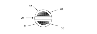
ダイヤモンドの基板は放熱板として作用する。異なるグレードの天然のダイヤモンド又は合成ダイヤモンドが市販されており、これらの熱伝導は異なるため、ダイヤモンドの放熱板としての効率に影響する。ダイヤモンドの熱伝導が高いほど今回の用途により適している。ダイヤモンドの厚みもまた、放熱板としての性能に影響を及ぼす。ダイヤモンドの厚みを調整して、機器で用いられる電子ビームのスポットの大きさの範囲に適するようにすることが可能である。アノード上のダイヤモンドの形状もまた、それぞれの要求に応じて変化させることが可能である。例えば、半円状のものを2つ用いて、2つのターゲットを有する形状のアノードや、例えばアルミニウムかマグネシウムX線を産生するために設計された電極に使用することができる。(図2参照、以下に述べる。) The diamond substrate acts as a heat sink. Different grades of natural diamond or synthetic diamond are commercially available and their thermal conduction is different, which affects the efficiency of diamond as a heat sink. The higher the thermal conductivity of diamond, the better it is for this application. The thickness of the diamond also affects the performance as a heat sink. The diamond thickness can be adjusted to suit the range of electron beam spot sizes used in the instrument. The shape of the diamond on the anode can also be varied according to the respective requirements. For example, two semicircular ones can be used for an anode shaped with two targets, or for an electrode designed to produce, for example, aluminum or magnesium x-rays. (See FIG. 2, described below.)
ダイヤモンドの特性は、最適な熱移動、及び/又は接着層や存在しうるいずれかの中間層との適合性に優れたものを提供するために選択するのが適切である。従って、ダイヤモンドメンバーは、300Kの下で少なくとも1200W/mkの熱伝導率を有するダイヤモンドを含むのが適切である。少なくとも1500W/mKのものが望ましく、少なくとも1700W/mKのものがより望ましく、少なくとも1800W/mKのものが最も望ましい。少なくとも、天然ダイヤモンドの2aタイプと同程度の熱伝導率のものが望ましい。 The properties of the diamond are suitably selected to provide optimum heat transfer and / or good compatibility with the adhesive layer and any intermediate layers that may be present. Accordingly, the diamond member suitably comprises diamond having a thermal conductivity of at least 1200 W / mk under 300K. It is preferably at least 1500 W / mK, more preferably at least 1700 W / mK, and most preferably at least 1800 W / mK. It is desirable to have at least the same thermal conductivity as the natural diamond 2a type.
ダイヤモンドの熱拡散率は、300Kの下で10cm2/sより大きなものが適切である。 It is appropriate that the thermal diffusivity of diamond is larger than 10 cm 2 / s under 300K.
ダイヤモンドメンバーは単結晶であることが適切である。 Suitably the diamond member is a single crystal.
ダイヤモンドメンバーは接着層より厚いことが望ましい。 The diamond member is preferably thicker than the adhesive layer.
典型的には、ダイヤモンドメンバーは50μm〜1000μmの範囲の厚みを有し、150μm〜800μmの範囲の厚みを有するのが望ましく、300μm〜500μmの範囲の厚みを有するのがより望ましく、400μm程度の厚みを有するのが最も望ましい。 Typically, the diamond member has a thickness in the range of 50 μm to 1000 μm, preferably has a thickness in the range of 150 μm to 800 μm, more preferably has a thickness in the range of 300 μm to 500 μm, and a thickness of about 400 μm. It is most desirable to have
所望の特性X線を発生させるためにターゲット層の選択を行う。ダイヤモンドとターゲット層の外側表面との間の熱伝導の障壁を削減するため、一般的に、ターゲット層はできる限り薄くするべきである。もっとも、アノード使用時に層が減耗することを考慮して、被膜の寿命を充分長くするために、ターゲット層にはある程度の厚みが必要である。 A target layer is selected in order to generate desired characteristic X-rays. In general, the target layer should be as thin as possible to reduce the thermal conduction barrier between the diamond and the outer surface of the target layer. However, in consideration of depletion of the layer when the anode is used, the target layer needs to have a certain thickness in order to sufficiently extend the life of the coating.
ターゲットはアルミニウム及びマグネシウムの少なくとも一つを含むことが適切である。特にアルミニウムが望ましい。ターゲットはアルミニウムを不可欠的に含むことが適切である。 Suitably the target comprises at least one of aluminum and magnesium. Aluminum is particularly desirable. It is appropriate that the target contains aluminum indispensably.
異なる特性、異なる波長のX線を発生させるため、アルミニウムやマグネシウムに加えて、又はその代わりに、他の物質を被膜として使用してもよい。かかる物質は、典型的には銀、ジルコニウム、及びタングステンの中から選ばれる。これらの被膜の一つ又は複数はアノード上に同時に存在してもよいが、離れたターゲット(例えば離れた領域)とするのが望ましい。複数のターゲットを有する構成として適切なものを図2a、2bに示す。 Other materials may be used as the coating in addition to or instead of aluminum or magnesium to generate X-rays with different properties and different wavelengths. Such materials are typically selected from silver, zirconium, and tungsten. One or more of these coatings may be present on the anode simultaneously, but are preferably remote targets (eg, remote areas). A suitable configuration having multiple targets is shown in FIGS. 2a and 2b.
所望の電圧をターゲットに印加しうる確実な一つの方法は、ターゲット物質を利用して、筐体に通じる導電路を供給することである。従って、ターゲットをダイヤモンドメンバーの上部面に設け、上部面から、ダイヤモンドメンバーの少なくとも一つの側面を通って、筐体まで伸び、ターゲットと筐体の間に電気的接触を形成することが望ましい。 One reliable way to apply the desired voltage to the target is to use a target material to provide a conductive path leading to the housing. Accordingly, it is desirable to provide a target on the upper surface of the diamond member and extend from the upper surface through at least one side of the diamond member to the housing to form an electrical contact between the target and the housing.
ターゲットは10μm〜200μmの範囲の厚みを有することが適切であり、20μm〜100μmの範囲の厚みが望ましく、35μm〜65μmの範囲の厚みがより望ましく、50μm程度の厚みが最も望ましい。 The target suitably has a thickness in the range of 10 μm to 200 μm, preferably in the range of 20 μm to 100 μm, more preferably in the range of 35 μm to 65 μm, and most preferably about 50 μm.
ダイヤモンドメンバーと筐体の接着を改善すると同様に、本発明の発明者は、ターゲットとダイヤモンドの間に中間層を提供することによって、信頼性、及び/又は熱の移動が改善されることを見付けた。このような中間層を接着層とダイヤモンド層の間の中間層とは別に提供することもできるが、かかる層をダイヤモンドメンバーの両方の側に提供することが望ましい。 As well as improving the adhesion between the diamond member and the housing, the inventors of the present invention have found that providing an intermediate layer between the target and the diamond improves reliability and / or heat transfer. It was. Although such an intermediate layer can be provided separately from the intermediate layer between the adhesive layer and the diamond layer, it is desirable to provide such a layer on both sides of the diamond member.
このように、第4の中間層はターゲットとダイヤモンドメンバーの間に設けるのが適切である。第4の中間層は、上述の第1の中間層として定義されたものである。 Thus, it is appropriate to provide the fourth intermediate layer between the target and the diamond member. The fourth intermediate layer is defined as the first intermediate layer described above.
第4の中間層の厚みは0.1μm程度であることが望ましい。 The thickness of the fourth intermediate layer is preferably about 0.1 μm.
第4の中間層は第1の中間層より厚いことが適切である。(第1の中間層が存在する場合には。−第4の中間層を設けるためには必ずしも必要でない。) Suitably the fourth intermediate layer is thicker than the first intermediate layer. (If the first intermediate layer is present. -Not necessarily required to provide the fourth intermediate layer.)
第4の中間層とターゲットとの間に第5の中間層を設けることによって、信頼性と高温下での性能を更に改善できることがわかった。 It has been found that by providing the fifth intermediate layer between the fourth intermediate layer and the target, the reliability and performance at high temperatures can be further improved.
このように、第5の中間層はターゲットと第4の中間層の間に設けることが望ましい。第5の中間層は上述の第2の中間層として定義されたものである。 Thus, it is desirable to provide the fifth intermediate layer between the target and the fourth intermediate layer. The fifth intermediate layer is defined as the second intermediate layer described above.
第5の中間層の厚みは0.1μm程度であることが望ましい。 The thickness of the fifth intermediate layer is preferably about 0.1 μm.
第5の中間層は第2の中間層より薄いことが適切である。 Suitably, the fifth intermediate layer is thinner than the second intermediate layer.
本発明の他の実施形態は、電子源と電極を有するX線発生装置において利用する電極における利用法を提供する。この電極は、
筐体と、
筐体上に取り付けられたダイヤモンドメンバーと、
ダイヤモンドメンバー上に取り付けられたターゲットと、
この文書内で定義される第1の中間層、第2の中間層、第3の中間層、第4の中間層、及び第5の中間層のいずれか一つ又は複数の接着層を有する。
Another embodiment of the present invention provides a method of using an electrode for use in an X-ray generator having an electron source and an electrode. This electrode
A housing,
A diamond member mounted on the housing;
A target mounted on a diamond member;
It has one or a plurality of adhesive layers of the first intermediate layer, the second intermediate layer, the third intermediate layer, the fourth intermediate layer, and the fifth intermediate layer defined in this document.
かかる利用法は、かかる電極の製造方法における利用法を含むのが適切である。 Such usage suitably includes usage in such an electrode manufacturing method.
本発明の他の実施形態は、電子源を有するX線発生装置において用いる電極を提供する。この電極は、
筐体と、
筐体上に取り付けられたダイヤモンドメンバーと、
ダイヤモンドメンバー上に取り付けられたターゲットと、
を有し、この電極は、さらに、この文書内で定義した接着層、第1の中間層、第2の中間層、第3の中間層、第4の中間層、及び第5の中間層のいずれか一つ又は複数を有する。
Another embodiment of the present invention provides an electrode for use in an X-ray generator having an electron source. This electrode
A housing,
A diamond member mounted on the housing;
A target mounted on a diamond member;
The electrode further comprises an adhesive layer, a first intermediate layer, a second intermediate layer, a third intermediate layer, a fourth intermediate layer, and a fifth intermediate layer as defined in this document. Any one or more.
特に、上述のように、本発明の発明者は、接着層とダイヤモンドメンバーの間の第1の中間層を利用することによって、XPSスペクトロメータ内の電極の信頼性と性能を著しく改善できることに気付いた。実際、本発明の発明者は、接着層が第1の実施形態によって定義されたものではない場合でも、かかる利点が得られることを発見した。従って、かかる中間層の利用はより広い適用性を有しており、金属を含むいかなる接着層とも同時に使用することができる。 In particular, as noted above, the inventor of the present invention has noticed that the reliability and performance of electrodes in an XPS spectrometer can be significantly improved by utilizing a first intermediate layer between the adhesion layer and the diamond member. It was. Indeed, the inventors of the present invention have found that such advantages are obtained even when the adhesive layer is not as defined by the first embodiment. Thus, the use of such an intermediate layer has broader applicability and can be used simultaneously with any adhesive layer containing metal.
従って、本発明の他の実施形態は、電子源を有するX線発生装置に用いられる電極を提供する。この電極は、
筐体と、
筐体上に取り付けられたダイヤモンドメンバーと、
ダイヤモンドメンバー上に取り付けられたターゲットとを有し、このターゲットは使用の際、X線を発生させるために電子源由来の電子に衝突されるものであり、金属を含む接着層が筐体とダイヤモンドメンバーとの間に設けられており、前記第1の中間層が接着層とダイヤモンドメンバーの間に設けられ、前記第1の中間層はチタンとクロミウムの少なくとも一つを有するものである。
Accordingly, another embodiment of the present invention provides an electrode for use in an X-ray generator having an electron source. This electrode
A housing,
A diamond member mounted on the housing;
A target mounted on a diamond member, which in use is bombarded by electrons from an electron source to generate X-rays, and an adhesive layer comprising a metal is formed between the housing and the diamond. The first intermediate layer is provided between the adhesive layer and the diamond member, and the first intermediate layer has at least one of titanium and chromium.
かかる接着層はいずれも合金を含むのが適切である。接着層は第1の実施形態で定義したものが望ましい。 Suitably any such adhesive layer comprises an alloy. The adhesive layer is preferably defined in the first embodiment.
第1の中間層は第1の実施形態で定義したものが望ましい。 The first intermediate layer is preferably defined in the first embodiment.
一つ又は複数の中間層を付加したものを用いることによる利点を本実施形態に適用することも可能である。従って、電極は、第1の実施形態における第2、第3、第4、及び第5の中間層のうち一つ又は複数を含むのが望ましい。 Advantages obtained by using one with one or more intermediate layers added can also be applied to this embodiment. Therefore, the electrode desirably includes one or more of the second, third, fourth, and fifth intermediate layers in the first embodiment.
同様に、ダイヤモンドメンバー、ターゲット、及び筐体のいずれか一つは第1の実施形態において定義されたものが望ましい。 Similarly, any one of the diamond member, the target, and the housing is preferably defined in the first embodiment.
本発明の他の実施形態は電子源を有するX線発生装置で用いられる電極を提供する。この電極は、
筐体と、
筐体上に取り付けられたダイヤモンドメンバーと、
ダイヤモンドメンバーの上に設けられたターゲットとを有し、このターゲットはX線を発生させるため、使用時には電子源由来の電子が衝突するものであり、接着層が筐体とダイヤモンドメンバーの間に設けられ、この接着層は、銀と銅、及び少なくとも一つの他の金属を付加したものを含む合金から成る。
Another embodiment of the present invention provides an electrode for use in an X-ray generator having an electron source. This electrode
A housing,
A diamond member mounted on the housing;
A target provided on a diamond member, and this target generates X-rays, so that electrons from an electron source collide during use, and an adhesive layer is provided between the casing and the diamond member. The adhesive layer is made of an alloy including silver and copper and at least one other metal added.
合金は銀、銅、及びインジウムを含むのが望ましい。また、銀−銅の共晶合金も望ましい。 The alloy preferably includes silver, copper, and indium. A silver-copper eutectic alloy is also desirable.
合金は、合金総重量に対して、55〜70重量%の銀、20〜35重量%のインジウムを含むことが適切である。他の実施形態において選択可能で望ましい特徴を本実施形態に適用することも望ましい。 Suitably the alloy contains 55-70 wt% silver, 20-35 wt% indium, based on the total weight of the alloy. It is also desirable to apply features that are selectable and desirable in other embodiments to this embodiment.
本発明の他の実施形態は、X線発生装置を供給し、前記装置は前記いずれかの実施形態で記載された電極と電子源を有し、使用時に電子が前記電子源から産生され、電極のターゲットに衝突しうるものである。 Another embodiment of the present invention provides an X-ray generation device, the device comprising the electrode and electron source described in any of the previous embodiments, wherein in use, electrons are produced from the electron source, and the electrode Can collide with other targets.
電子源はフィラメントを有するのが適切である。 Suitably the electron source comprises a filament.
装置は電子をターゲットに向けて加速する加速手段を有するのが望ましい。 The apparatus preferably has acceleration means for accelerating the electrons toward the target.
装置は電子源に対して正の電位を電極に供給する電圧供給手段を有するのが適切である。典型的には、正の電位とは少なくとも10kVであり、15kV程度が望ましい。 Suitably the apparatus comprises voltage supply means for supplying a positive potential to the electrode relative to the electron source. Typically, the positive potential is at least 10 kV, preferably about 15 kV.
電子源はアースされていることが望ましい。その代わりにアノードをアースすることもでき、その場合には電子源(典型的にはフィラメント)を負の電位にしておく。アノードは電子源に対して10〜15kVの正の電位にされることが適切である。 The electron source is preferably grounded. Alternatively, the anode can be grounded, in which case the electron source (typically the filament) is kept at a negative potential. Suitably the anode is at a positive potential of 10-15 kV relative to the electron source.
電極上の電子ビームの大きさ(「スポットサイズ」)は、直径1μmないしはそれ未満のサイズから、大きい場合は、電極面(適切にはターゲット面)のサイズ(直径がほぼ10mmのオーダーのものが標準的である)になりうる。しかし、電子ビームはアノード表面より著しく小さい方が都合がよい。従って、スポットサイズは約0.5mm x1mmが望ましい。 The size of the electron beam on the electrode (“spot size”) is from 1 μm or less in diameter and, if large, the size of the electrode surface (suitably the target surface) (with a diameter on the order of approximately 10 mm). Can be standard). However, it is convenient for the electron beam to be significantly smaller than the anode surface. Therefore, the spot size is preferably about 0.5 mm × 1 mm.
装置は電子をターゲット上に方向付ける電子光学素子を有することが適切である。電子をターゲットのターゲット領域に方向付けるように電子光学素子を含むことが望ましい。ターゲット領域は少なくとも0.15mm2であり、少なくとも0.35mm2がより望ましく、最も望ましいのは少なくとも0.45mm2である。 Suitably the apparatus comprises an electro-optic element that directs electrons onto the target. It is desirable to include an electro-optic element to direct electrons to the target area of the target. Target area is at least 0.15 mm 2, at least 0.35 mm 2 and more preferably, most desirably at least 0.45 mm 2.
スポットの大きさは固定でも可変でもよい。望ましい実施例は、スポットの大きさを変えて供給できるように構成された装置である。例えば、異なる大きさの試料を分析できるよう、装置はスポットの大きさを実験ごとに変更可能なスポットサイズ変更手段を有することが適切である。 The spot size may be fixed or variable. A preferred embodiment is an apparatus configured to be able to supply with varying spot sizes. For example, it is appropriate that the apparatus has spot size changing means capable of changing the spot size for each experiment so that samples of different sizes can be analyzed.
スポットの大きさを固定することは、試料の光電子パラレルイメージを生成する際に望ましい。即ち、パラレルイメージの記録時にはスポットを固定するのが望ましい。実験ごとにスポットの大きさを変更可能だが、イメージ記録時には変更を行わない。同様に、スペクトル記録時にもスポットの大きさが固定されるのが望ましい。 Fixing the spot size is desirable when generating an optoelectronic parallel image of the sample. That is, it is desirable to fix the spot when recording a parallel image. The spot size can be changed for each experiment, but it is not changed during image recording. Similarly, it is desirable that the spot size is fixed during spectrum recording.
スポットの大きさを変更できると、選択した領域から、より高品質のスペクトルを得ることができる。即ち、同一の測定時間内に得られる信号対雑音比が向上したスペクトルを得られる。それに加え、スポットが大きいと、パラレルイメージを記録するのに用いることができ、また、別の実験では、より小さなスポットを使用して試料上のより小さな特定の領域からより高品質なデータを得ることができる。 If the spot size can be changed, a higher quality spectrum can be obtained from the selected region. That is, a spectrum with an improved signal-to-noise ratio obtained within the same measurement time can be obtained. In addition, large spots can be used to record parallel images, and in other experiments, smaller spots are used to obtain higher quality data from smaller specific areas on the sample. be able to.
電子ビームの形状(断面)は、典型的には円形か長方形であるが、電子ビーム光学素子を調整することによっていかなる形状にすることも可能である。 The shape (cross section) of the electron beam is typically circular or rectangular, but any shape can be obtained by adjusting the electron beam optical element.
電子ビームは電極の一定の固定した場所に衝突する。または、アノード上の一定の範囲の場所に方向付けるように制御することもできる(即ち、スポット位置を変更できる)。このように、一定の範囲の場所を通る様に電子ビームの走査を調整することもできる。ビームを制御できることによって、アノードの使用可能な耐用期間を延ばすことができるという利点も得られる。なぜなら、電子ビームが衝突する部分のアノード表面は時間とともに損傷を受けるからである。従って、望ましい実施例は、アノード上の電子ビームスポットの場所を制御することのできる電子ビーム制御器を有する。電子ビーム制御器は、電子ビームスポットをアノード上で走査するのに特に適するものである。 The electron beam strikes a fixed location on the electrode. Alternatively, it can be controlled to direct to a certain range of locations on the anode (ie, the spot position can be changed). Thus, the scanning of the electron beam can be adjusted so as to pass through a certain range of locations. The ability to control the beam also has the advantage of extending the usable life of the anode. This is because the anode surface where the electron beam collides is damaged with time. Therefore, the preferred embodiment has an electron beam controller that can control the location of the electron beam spot on the anode. The electron beam controller is particularly suitable for scanning an electron beam spot over the anode.
別の実施例では、アノードの位置を電子ビームに対応させて変化させるためアノードを移動する。アノード上に照射されるスポットはモノクロメータとの関係では、すなわち試料や分析器の分析物の位置との関係では移動しないため、かかる構成は有用である。これによって、アノードの使用可能期間が伸びる。装置にはアノードを移動させるアノード移動手段が含まれるのが適切である。 In another embodiment, the anode is moved to change the position of the anode in response to the electron beam. Such a configuration is useful because the spot illuminated on the anode does not move in relation to the monochromator, i.e., in relation to the position of the analyte in the sample or analyzer. This extends the usable life of the anode. Suitably the apparatus includes anode moving means for moving the anode.
装置は球面鏡分析器を有するのが望ましく、半球形分析器も有することが望ましい。これらの用語は当業者には周知のものである。球面鏡分析器及び半球形分析器として適切なものは特許文献GB−A−2244369に記載されている。装置は特許文献GB−A−2244369に記載の電子分析器を有することが望ましい。 The apparatus preferably has a spherical mirror analyzer and preferably also has a hemispherical analyzer. These terms are well known to those skilled in the art. Appropriate spherical mirror analyzers and hemispherical analyzers are described in patent document GB-A-2244369. The apparatus preferably has an electronic analyzer described in Patent Document GB-A-2244369.
装置は遅延線検出器を有することが望ましい。適切な遅延線検出器は特許文献GB−A−2397940に記載されている。 The apparatus preferably has a delay line detector. A suitable delay line detector is described in patent document GB-A-2379940.
電極からの熱の除去に役立たせるため、装置は冷却液を電極に供給する冷却液手段を有することが望ましい。 In order to assist in the removal of heat from the electrodes, it is desirable for the apparatus to have coolant means for supplying coolant to the electrodes.
装置はX線モノクロメータを有することが望ましい。 The apparatus preferably has an X-ray monochromator.
さらに別の実施形態において、本発明は前記の実施形態のいずれか一つに記載された電極を有するX線光電子分光計を提供する。 In yet another embodiment, the present invention provides an X-ray photoelectron spectrometer having an electrode as described in any one of the previous embodiments.
さらに別の実施形態において、本発明は前記の実施形態のいずれか一つに記載された電極または装置を用いたX線発生方法を提供する。 In yet another embodiment, the present invention provides an X-ray generation method using the electrode or apparatus described in any one of the above embodiments.
さらに別の実施形態において、本発明は前記の実施形態のいずれか一つに記載された電極または装置を用いたX線光電子分光方法を提供する。 In yet another embodiment, the present invention provides an X-ray photoelectron spectroscopy method using the electrode or apparatus described in any one of the above embodiments.
かかる方法では、電極を水で冷却し、電極内の水の温度を沸点より下に維持することが望ましい。 In such a method, it is desirable to cool the electrode with water and maintain the temperature of the water in the electrode below the boiling point.
ここで開示した、接着方法に関する様々な改善例に基づく利点のみならず、本発明の発明者は、ターゲットと筐体の間にダイヤモンドメンバーを設けた電極が、球面鏡分析器と遅延線検出器を有するX線光電子分光計に用いられた場合、X線のカウント、信号対雑音比、及びイメージ産生の点で特に優れた結果が得られることを見いだした。実際問題としては、かかる装置では、ここで検討した接着層及び/又は中間層を欠く場合でも、驚くべき優れた結果が得られることを、本発明の発明者は発見した。このように、分光計のかかるナロークラスはダイヤモンドを含むアノードを用いることによって性能を改善するのに適している。 In addition to the advantages based on the various improvements related to the bonding method disclosed herein, the inventors of the present invention have the advantage that an electrode provided with a diamond member between a target and a case has a spherical mirror analyzer and a delay line detector. When used in an X-ray photoelectron spectrometer, it has been found that particularly excellent results are obtained in terms of X-ray count, signal-to-noise ratio, and image production. In practice, the inventors of the present invention have found that such devices can provide surprisingly good results even in the absence of the adhesive and / or intermediate layers discussed herein. Thus, such a narrow class of spectrometers is suitable for improving performance by using an anode containing diamond.
さらに別の実施形態において、本発明はX線源と、球面鏡分析器と、遅延線検出器とを有するX線光電子分光計を提供し、前記X線源は電子源と電極を有するものであり、前記電極は
筐体と、
筐体上に取り付けられたダイヤモンドメンバーと、
ダイヤモンドメンバー上に設けられたターゲットとを有し、
前記ターゲットは使用時にはX線を発生させるため電子源由来の電子の衝突を受ける電極である。
In yet another embodiment, the present invention provides an X-ray photoelectron spectrometer having an X-ray source, a spherical mirror analyzer, and a delay line detector, the X-ray source having an electron source and an electrode. The electrode has a housing;
A diamond member mounted on the housing;
And a target provided on the diamond member,
The target is an electrode that receives collisions of electrons derived from an electron source in order to generate X-rays when used.
筐体、ターゲット、及びダイヤモンドメンバーのうちいずれかは前記の実施形態で定義されたものであることが適切である。 Any one of the housing, the target, and the diamond member is appropriately defined in the above embodiment.
分光計はX線モノクロメータを有することが望ましい。 The spectrometer preferably has an X-ray monochromator.
分光計を試料のイメージを得られるように構成、設定することが望ましい。 It is desirable to configure and set up the spectrometer so that an image of the sample can be obtained.
分光計は半球形分析器を有することが適切である。 Suitably the spectrometer has a hemispherical analyzer.
前記の実施形態はそれぞれ、他の実施形態の一つ、又は複数、又は全てと組み合わせてもよく、それぞれの実施形態における特徴は他の実施形態の特徴と組み合わせてもよい。 Each of the above embodiments may be combined with one, a plurality, or all of the other embodiments, and the features in each embodiment may be combined with the features of the other embodiments.
本発明の実施例を以下の図を参照しつつ具体例のみを用いて以下に記載する。 Embodiments of the present invention are described below using only specific examples with reference to the following figures.
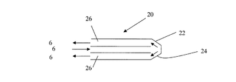
図1の電極1は銅製の筐体3を有する。筐体は、筐体内を伸びる、水路又は内腔5を形成する管を有する。使用時には、冷却液(典型的には水)が、水路/内腔5の内部を流れ、筐体から熱を取り除く(矢印6として示されている)。筐体のターゲット端部7(使用時にはターゲット端部7には電子ビーム8が衝突してX線9を産生する)で、ダイヤモンドの薄い基板10が筐体に取り付けられている。
The electrode 1 in FIG. 1 has a
筐体の拡大図はダイヤモンド基板10の断面図を示している。この厚みは400μmだが、他の厚み、例えば50μmから1mmでも使用可能である。接着層11を介して筐体3に取り付けられている。
The enlarged view of the housing shows a cross-sectional view of the
接着層11は50μmの厚みのろう付け用In10から成る。ろう付け用In10は、Ag(63%)、Cu(27%)、In(10%)を含むものであり、Johnson Mattheyで入手可能である。もっとも、Ag、Cu、Inは他の相対量でも使用可能である。In10の溶融温度の範囲は685〜730℃である(即ち、固相線が685℃、液相線が730℃である)。代わりに、同様の固相線や同様の溶融温度範囲を有する他の合金を使用してもよい。
The
これまで記載したように、金属とダイヤモンドの熱膨張係数の差は非常に大きいのが典型であり、かかる大きなストレスが接合部に生じれば接着部に不具合が生じるため、本発明の発明者は、金属とダイヤモンド、又は金属で被膜したダイヤモンド(金属の薄層で被膜されたダイヤモンド)との間に接着部を形成するのが困難であることに気付いた。しかし、本発明の発明者はろう付け用In10、または同様の特性を有するろう材は、ダイヤモンドとアノード本体の間を使用時の高温下においても、驚くほど強固で頑丈に接着することを見付けた。特に、本発明の発明者はろう付け用In10の固相線が比較的低い(685℃)という点が、かかる確実で高温に耐性ある接着を得るのに重要であることを明らかにした。 As described above, the difference between the thermal expansion coefficients of metal and diamond is typically very large, and if such a large stress occurs in the joint, a problem occurs in the bonded portion. It has been found that it is difficult to form a bond between metal and diamond, or diamond coated with metal (diamond coated with a thin layer of metal). However, the inventor of the present invention has found that brazing In10, or a brazing material having similar properties, has a surprisingly strong and robust bond between diamond and the anode body, even at high temperatures during use. . In particular, the inventors of the present invention have clarified that the fact that the solidus line of brazing In10 is relatively low (685 ° C.) is important for obtaining such a reliable and high temperature resistant bond.
このように、ろう付け用In10の主要な役割は、ダイヤモンドをアノード本体に接着することである。しかし、驚くべきことに、ろう付け用In10には、高温でアノードを使用する際に銅製のアノード本体とダイヤモンドの熱膨張の差によって生じる応力を減少させる性質を有することが発見された。In10の合金は比較的溶融温度が低く、それに応じて熱膨張も低いと考えられている。このことは、ダイヤモンドの熱膨張(特性)を補完し、それによって応力を減じるため、特に有益であることが分かった。このように、ろう付け用In10は熱膨張率が低く、この点でダイヤモンドに類似するため、特に優れている。かかる特性によって、ろうが確実にダイヤモンドにしっかりと接着するようになるのみならず、いかなる応力がろうのなかで発生しても、確実に金属との接合部でもしっかりと接着するようになる。ここでの接着は、ダイヤモンドとの接合部におけるものよりずっと強固である。銀と銅のありふれた合金(インジウムを含まないもの)も同様の作用を奏するが、溶融点が高いため、わずかだか望ましくない。 Thus, the primary role of the brazing In10 is to adhere diamond to the anode body. Surprisingly, however, it has been discovered that brazing In10 has the property of reducing the stress caused by the difference in thermal expansion between the copper anode body and diamond when the anode is used at high temperatures. An alloy of In10 is considered to have a relatively low melting temperature and correspondingly low thermal expansion. This has been found to be particularly beneficial because it complements the thermal expansion (characteristic) of diamond and thereby reduces stress. Thus, In10 for brazing is particularly excellent because it has a low coefficient of thermal expansion and is similar to diamond in this respect. Such properties not only ensure that the braze adheres securely to the diamond, but also ensure that it adheres securely at the joint with the metal no matter what stress occurs in the braze. The adhesion here is much stronger than at the joint with diamond. Common alloys of silver and copper (which do not contain indium) also have the same effect, but are slightly less desirable due to their high melting point.
実際、本発明の発明者は、ろうの溶融点が低いほど、熱膨張が小さくなって応力が小さくなるため、ダイヤモンドと金属筐体との接着が成功することが多くなることに気付いた。しかし、ダイヤモンド、合金(ろう)、金属筐体は全て使用時に高温になるため、合金(ろう)の溶融点をあまり低くすることはできない。さもないと、アノード使用時に合金が再溶融してしまう。 In fact, the inventor of the present invention has found that the lower the melting point of the wax, the more often the bond between the diamond and the metal housing is more successful because the thermal expansion is reduced and the stress is reduced. However, since diamond, alloy (brazing), and metal casing all have high temperatures during use, the melting point of the alloy (brazing) cannot be made too low. Otherwise, the alloy will remelt when the anode is used.
ターゲット13は、ダイヤモンド基板上の接着層11とは反対の面で、ターゲット層の形状でダイヤモンド基板に接着している。ターゲット層はAlから成り、厚み50μmである。
The
従って、ダイヤモンド基板の一表面は、使用の際に冷却される筐体3に接着される。電極はXPSを実施できる機器(この機器はこの分析手法のみを実施するものでも、他の分析手法も実施するものでもよい)の真空室の内部で用いる。望ましい実施例(図5、6で示されたようなもの)では、XPS機器は球面鏡分析器(SMA)を用いる。更に、XPS機器は球面鏡分析器及び遅延線検出器(DLD)を有することが望ましい。DLDの具体例は特許文献GB−A−2397940に記載された種類である(かかる構成を図5、6に示す)。
Accordingly, one surface of the diamond substrate is bonded to the
実際には、本発明の発明者は、図1に示すように、接着層11によって電極の筐体に接着させたダイヤモンドメンバーを有する電極を用いると、より高い感度を得ることができることに気付いた。特に、「通常の」電極を用いた場合と比較して信号対雑音に優れるため、更に有用な像やスペクトルを得ることができる。
In fact, the inventor of the present invention has realized that higher sensitivity can be obtained using an electrode having a diamond member bonded to the housing of the electrode by an
使用の際には、電極に電子発生に用いるフィラメントに対して正の電圧を印加すると、電子ビームが電極のターゲット13(例えば外側の金属被膜)に衝突することによってX線が発生する。以上のように、本実施例では電極はアノードとなっている。本実施例ではスポットの大きさは0.5mmx1mm程度であるが、他のサイズ及び形状も用いることができる。 In use, when a positive voltage is applied to the electrode used to generate electrons, the electron beam collides with the electrode target 13 (for example, an outer metal film) to generate X-rays. As described above, in this embodiment, the electrode is an anode. In this embodiment, the spot size is about 0.5 mm × 1 mm, but other sizes and shapes can be used.
上で言及したように、X線産生の効率はかなり悪く、従って電子ビームが有するエネルギーの大部分はアノードにおいて熱として消費されてしまう。アノード表面で発生する熱が累積すると、最終的には外部の金属被膜の溶融及び/又は昇華が引き起こされる。 As mentioned above, the efficiency of X-ray production is rather poor, so most of the energy that the electron beam has is consumed as heat at the anode. Accumulation of heat generated at the anode surface eventually causes melting and / or sublimation of the outer metal coating.
しかし、図1におけるダイヤモンド基板10のようなダイヤモンドメンバーを上記のAg・Cu・Inから成るろうのような接着層でアノード本体(筐体)に取り付けることによって、アノードの構造上の完全性を保持しつつ、アノード表面で発生する熱をより効率的に消失させることができる。従って、このような設計によって、アノードにおけるパワー密度が上昇するという結果が生じる。これは、このような設計を用いることによって、アノードから発生するX線の光量をより高めることが可能になることを意味する。
However, the structural integrity of the anode is maintained by attaching a diamond member such as the
合成ダイヤモンドの基板10は直径10mmの円形である。このため、大きな静止スポット(stationary spot)を利用することが可能になる。これは、例えば光電子のイメージ、望ましくは試料の光電子のリアルタイムイメージを産生する為に、アノードを球面鏡分析器と共に用いる場合に利点となることが分かってきた。
The
外側の金属被膜(ターゲット13)はダイヤモンド基板(図示なし)のサイドに伸びており、そこでアノード筐体3と電気的な接触を形成する。
The outer metal coating (target 13) extends to the side of the diamond substrate (not shown) where it makes electrical contact with the
ダイヤモンド基板の真下にある銅のアノード本体の厚みは約1.5mmである。ダイヤモンドの下にある銅の内部表面は冷却液(水)に接する表面を有する。このように、銅の内部表面は水によって冷却されている。 The thickness of the copper anode body directly under the diamond substrate is about 1.5 mm. The inner surface of the copper under the diamond has a surface in contact with the coolant (water). Thus, the copper inner surface is cooled by water.
アノード1の製造過程を以下に記す。最初に、ダイヤモンド基板10をIn10のろう付け層11を介して銅のアノード筐体3にろう付けする。次に、ダイヤモンドの上部表面をアルミニウムで被膜し、ターゲット13を形成する。
The manufacturing process of the anode 1 will be described below. First, the
最初にダイヤモンド(筐体に接着することになっている面)をTiで被膜し、次にPtとAuで被膜する。各層の被膜化の工程はイオンめっきによる。次に、In10を用いてダイヤモンドをアノード本体にろう付けする。ろう付けの作業中ダイヤモンドの場所がずれないよう、アノード本体はダイヤモンドを設置する収納部を有する。さらに、ろう付けの作業中ダイヤモンドの場所がずれないように、ダイヤモンドに穏やかな圧をかける(例えばダイヤモンドを定まった場所に固定する)。このような加圧(固定)は、ダイヤモンドの表面全体に、均一かつ完全にろう付けを行う助けにもなる。 First, diamond (surface to be bonded to the housing) is coated with Ti, and then coated with Pt and Au. The process of coating each layer is by ion plating. Next, diamond is brazed to the anode body using In10. The anode body has a storage portion for installing diamond so that the location of the diamond does not shift during the brazing operation. Furthermore, a gentle pressure is applied to the diamond so that the diamond does not shift during the brazing operation (for example, the diamond is fixed in place). Such pressing (fixing) also helps to braze the entire surface of the diamond uniformly and completely.
In10のろうを用いたろう付けの工程は、アノードの制限された部分のみを確実にろう付け温度まで加熱させるため、RF発生ろう付け機を用いて真空で行われる。他のろう付け過程や機械を用いることも可能である。素材及び/又はろうが異なる場合は尚更である。 The brazing process using In10 brazing is performed in a vacuum using an RF generating brazing machine to ensure that only a limited portion of the anode is heated to the brazing temperature. It is also possible to use other brazing processes and machines. This is even more true if the material and / or wax is different.
ダイヤモンドを一旦アノード本体にろう付けすると、ダイヤモンドの上部表面及び側面はTi、Pt、Alの各金属の層で被膜される。各層で用いられる被膜の工程はイオンプレーティングによる。 Once diamond is brazed to the anode body, the upper surface and sides of the diamond are coated with layers of Ti, Pt, and Al metals. The coating process used in each layer is by ion plating.
図2a、2bにおいて、電極20は2つのターゲット表面を有しており、各表面は管26を流れる水で冷却される。図2bにおいて、第1のターゲット表面22は、アルミニウムで形成された半円状のターゲット層28を含む。第2のターゲット表面24は、マグネシウムで形成された半円状のターゲット層30を含む。いずれのターゲット層も対応する形のダイヤモンドメンバー(図示なし)と接着している。
In FIGS. 2 a and 2 b, the
上で述べたように、アノード本体/筐体3は冷却液用の水路を有するため、冷却液水路と、中にアノードを有する真空室の間は超高真空によって密閉されている。
As described above, since the anode body /
アノード筐体には、アルミニウムのターゲット層の冷却を最大にするため、熱伝導率の高いマテリアルが用いられるのが適切である。望ましい実施例(例えば、図1、2a、3参照)では、アノードは銅製であり、水で冷却されている。他の冷却液を用いることも可能である。ダイヤモンドの下の銅の厚み及び液の水路の設計は、それぞれのアノードの設計及びアノードに衝突する電子ビームスポットのサイズに合わせて最適化することができる。アノード本体を形成する素材は他のものを使用してもよい。代替する最適な素材は、銀、タングステン、モリブデン、タンタル、ニオブ、レニウムのような、高い熱伝導率を有するものである。 For the anode housing, it is appropriate to use a material with high thermal conductivity in order to maximize the cooling of the aluminum target layer. In the preferred embodiment (see, eg, FIGS. 1, 2a and 3), the anode is made of copper and cooled with water. Other cooling liquids can also be used. The thickness of the copper under the diamond and the design of the liquid channel can be optimized for each anode design and the size of the electron beam spot impinging on the anode. Other materials may be used for forming the anode body. The best alternative materials are those with high thermal conductivity, such as silver, tungsten, molybdenum, tantalum, niobium, rhenium.
ダイヤモンド基板は放熱板として作用する。天然又は合成の様々なグレードのダイヤモンドが市販されており、これらは熱伝導率が異なるため、放熱板としての効率に影響する。一般的に、ダイヤモンドの熱伝導率が高いほど今回の用途には適している。ダイヤモンドの厚みも熱放板としての性能に影響する。ダイヤモンドの厚みは、機器で用いられる電子ビームのスポットの大きさの範囲に適合するように調整することができる。アノード上のダイヤモンドの形状も、それぞれの機器に適合するように変更することができる。例えば、アルミニウム、又はマグネシウムのいずれかのX線を産生するように設計された、形状の異なるアノードには、半円状のものを2つ使用することができる(図2参照)。 The diamond substrate acts as a heat sink. Various grades of natural or synthetic diamond are commercially available, which have different thermal conductivities and thus affect the efficiency as a heat sink. Generally, the higher the thermal conductivity of diamond, the better it is for this application. The thickness of diamond also affects the performance as a heat release plate. The thickness of the diamond can be adjusted to suit the range of electron beam spot sizes used in the instrument. The shape of the diamond on the anode can also be varied to suit the respective equipment. For example, two semicircular anodes can be used for differently shaped anodes designed to produce either aluminum or magnesium x-rays (see FIG. 2).
アノードの設計は大きく変更することが可能であり、他の設計としては、冷却液がダイヤモンドの一つの表面の大部分と接触するように、アノードの銅製の本体の端部にある穴を覆うようにダイヤモンドを固定するものがある。図3はかかる変更例を示している。電極40は、使用時に水(又は他の液体)の流れる管44を含む筐体42を有している。ダイヤモンドメンバー46は筐体の開口48の上に取り付けられており、使用時にはダイヤモンドメンバーが直接冷却液に接触できるようになっている。ダイヤモンドメンバー46はフランジ50の部分で筐体に接着している。ダイヤモンドとアノード本体の間は、超高真空基準で真空密閉されている。ダイヤモンドとアノード筐体のフランジとの間でも上記と同様の接着が行われている。
The anode design can vary greatly, and other designs cover the hole at the end of the copper body of the anode so that the coolant is in contact with the majority of one surface of the diamond. There are some that fix diamonds. FIG. 3 shows such a modification. The
この構成におけるダイヤモンドの最適な厚みは、その正確な設計によって変わる。 The optimum diamond thickness in this configuration depends on its exact design.
本発明の取り組むもう一つの重要な課題は、ダイヤモンド上の被膜を高品質に(すなわち、ターゲットを高品質に)形成することである。 Another important challenge addressed by the present invention is to form a coating on diamond with high quality (ie, high quality target).
以上のように、本発明の発明者は、例えば適切なろう(接着層)がダイヤモンドの表面に対して直接ではなく、中間層に対して塗布された場合に、より強固な領域が形成されることを観察した。同様に、本発明の発明者は、ダイヤモンドとターゲット(例えばアルミニウム)の間に中間体となる被膜を形成すれば、接着がより強固になり、ターゲットの耐久性もより増加することを見付けた(このようにしなければ、アノード使用時にターゲットが剥がれやすくなる)。このように、中間層を提供する(ダイヤモンドを金属で被膜する)ことによって、アノードを機器に取り付ける際にターゲットの被膜に損傷が生じる危険性が減少する。 As described above, the inventor of the present invention forms a stronger region when, for example, a suitable brazing (adhesive layer) is applied directly to the intermediate layer rather than directly to the diamond surface. Observed that. Similarly, the inventors of the present invention have found that if an intermediate film is formed between diamond and a target (for example, aluminum), the adhesion becomes stronger and the durability of the target also increases ( If this is not done, the target will easily peel off when the anode is used). Thus, providing an intermediate layer (coating diamond with metal) reduces the risk of damage to the target coating when the anode is attached to the instrument.
図4に示す実施例において(詳細は以下で述べる)、まず初めにダイヤモンドをチタンの薄層で被膜する。チタンによってダイヤモンドへの接着を強固にすることができる。ダイヤモンドを一旦チタンで被膜すると、他の素材はチタン層によく接着するため、他の被膜を塗布することも可能である。このように、チタンはダイヤモンドに強力に接着するため、他の素材が構造に接着できるようにするために使用される。クロムのような、チタン以外の材質もこの目的のために使用できるかもしれない。ダイヤモンドと銅との熱伝導率の垣根を下げるために、チタンの層はできる限り薄くすることが望ましい。(ダイヤモンドとアルミニウムの間でも同様である)。チタンは、ダイヤモンドに被膜を提供し、他の素材が構造に接着できるよう、充分な厚みを有することが必要である。 In the embodiment shown in FIG. 4 (details will be described below), diamond is first coated with a thin layer of titanium. Titanium can strengthen adhesion to diamond. Once the diamond is coated with titanium, other materials adhere well to the titanium layer, so other coatings can be applied. In this way, titanium adheres strongly to diamond and is used to allow other materials to adhere to the structure. Materials other than titanium, such as chrome, may also be used for this purpose. To lower the thermal conductivity barrier between diamond and copper, it is desirable to make the titanium layer as thin as possible. (The same is true between diamond and aluminum). Titanium needs to be thick enough to provide a coating on the diamond and allow other materials to adhere to the structure.
第1の中間層(典型的にはチタン)にさらに中間層を塗布することで、信頼性と接着強度を更に改善することができる。従って、チタン層を覆うために厚いプラチナの層を塗布することが望ましい。プラチナ層がバリア層となって、次の層がチタン層に拡散(又は混合)したりその逆が生じたりすることを予防する。プラチナ層はバリア層として使用され、アノードが使用されてその結果温度上昇(200〜600℃)が生じる際に他の層がバリアを越えて拡散するのを防いでいる。種々の層の拡散、及びその結果生じる混合によって、その性能が低下するため、かかる事態を防がなければならない。ダイヤモンドとアルミニウムと銅の間の熱伝導率の垣根を抑えるため、プラチナ層はできる限り薄くするのが望ましい。プラチナ層は拡散を効率的に防ぐバリアとなるに充分な厚みを有することが望ましい。タングステンのような他の素材もバリア層として用いることができる。 By further applying an intermediate layer to the first intermediate layer (typically titanium), the reliability and adhesive strength can be further improved. Therefore, it is desirable to apply a thick platinum layer to cover the titanium layer. The platinum layer acts as a barrier layer to prevent the next layer from diffusing (or mixing) into the titanium layer and vice versa. The platinum layer is used as a barrier layer, preventing other layers from diffusing across the barrier when the anode is used resulting in a temperature rise (200-600 ° C.). Such a situation must be prevented because the diffusion of the various layers and the resulting mixing degrades its performance. In order to reduce the thermal conductivity barrier between diamond, aluminum and copper, it is desirable to make the platinum layer as thin as possible. The platinum layer is desirably thick enough to provide a barrier that effectively prevents diffusion. Other materials such as tungsten can also be used as the barrier layer.
接着の信頼性と強度をさらに改善するため、ダイヤモンドを第3の層で覆うことも可能である。筐体に接着しているダイヤモンドの表面上に形成する第3の層は金である。この金の層は、さらに、接着層(ろう)と被膜されたダイヤモンドとの間の接着を強固に形成することを目的としている。金の層は、ろう(例えば、In10)に対してダイヤモンドの被膜された構造がより強固に接着するように改善するために用いられる。ダイヤモンドとアノード本体との間の熱伝導率の垣根を抑えるため、この層はできる限り薄くするのが望ましい。この層はろうとダイヤモンド被膜された組立部との間の接着を優れたものとするのに充分な厚みを有することが望ましい。ろうへの接着を改善するために他の素材を被膜として用いてもよい。 It is also possible to cover the diamond with a third layer to further improve the reliability and strength of bonding. The third layer formed on the surface of the diamond bonded to the housing is gold. The gold layer is further intended to form a strong bond between the adhesive layer (brazing) and the coated diamond. The gold layer is used to improve the diamond-coated structure to adhere more tightly to the braze (eg, In10). In order to reduce the thermal conductivity barrier between the diamond and the anode body, it is desirable to make this layer as thin as possible. This layer preferably has a thickness sufficient to provide excellent adhesion between the braze and the diamond coated assembly. Other materials may be used as the coating to improve adhesion to the wax.
かかる望ましい特徴を念頭に置き、図4は上述のような中間層を有する電極60を示している。このように、ダイヤモンド基板62(TM180合成ダイヤモンド、厚み400μm、Element Six B.Vから入手)はTi 層66(厚み0.06μm)、Pt層68(厚み0.12μm)、Au層70(厚み1μm)、及びIn10のろう層72(厚み50μm)を介して銅の筐体64に接着されている。
With such desirable features in mind, FIG. 4 shows an
ダイヤモンド基板62の反対側の表面には、Ti層74(厚み0.1μm)とPt層76(厚み0.1μm)が、ダイヤモンドと、Alから成るターゲット層78(厚み50μm)との間に存在する。この構成では、ダイヤモンドとアノード筐体とAlのターゲット層との間の接着が特に頑丈になる。X線を発生する機器(例えば、XPS装置)で用いると、ダイヤモンドと接着層によって優れた熱放散がもたらされるため、より多くのX線を発生させることができる。
On the opposite surface of the
上述のように、様々な層、とくに接着層は、例えばエレクトロニクス産業におけるろうよりも遙かに高温(例えば200℃〜650℃)にさらされる。 As mentioned above, the various layers, especially adhesive layers, are exposed to much higher temperatures (eg, 200 ° C. to 650 ° C.) than waxes in the electronics industry, for example.
図5はXPS機器100を示しており、その中ではアノード101がX線発生源102内部で使用されている。X線源は、アノード、及びアノードの方にに方向付けできる電子ビームを発生させる電子ビーム発生器(本実施例では加熱したフィラメント。図示なし。)を有する。アノード101にはフィラメントに対して正の電位が印加されており、例えば望ましい実施例では15000Vが印加されている。電子ビームの衝突するアノードの外側の被膜によって、発生するX線の特性が異なってくる。アノード上のスポットの大きさは電子ビーム発生器とアノードの間に設けられた電子光学素子(図示なし)の配置により制御できる。上述のように、アノード上の電子ビームのスポットの大きさは本実施例では固定されているが、変更することも可能である。アノード101は磁場レンズ103の近傍に配置するのが適切である。磁場レンズはX線源の一部をなすものではない。磁場レンズは分析器の電子光学素子を構成するレンズの一つである。磁場レンズによって電子は分析器の方向に導かれる。
FIG. 5 shows an
X線源は、X線モノクロメータに組み込んで利用される。X線モノクロメータは、エネルギー範囲を狭くし、X線源から放出されたX線ビームをフォーカスさせる。このように、本実施例の機器はX線モノクロメータを有する(図示なし)。その代わり、X線ビームがXPS分析が行われる試料の方向に直接放出されるようにX線源を設計してもよい(図示あり)。かかる構成では、薄い金属箔(典型的には アルミニウム又はベリリウム)をアノードと試料の間に設置してX線源の一部としてもよい。実際、XPSの機器は両タイプのX線源の一つまたは複数を有していてもよい。このように、機器は、エネルギー分散を制限したフォーカスX線スポットを使用するために、X線モノクロメータを利用したアルミニウムX線源を装備してもよく、また、試料に、フォーカスしていないX線を直接照射する(試料を大量の光にさらす)ために、アルミニウムとマグネシウムのデュアルX線源を装備してもよい。 The X-ray source is used by being incorporated in an X-ray monochromator. The X-ray monochromator narrows the energy range and focuses the X-ray beam emitted from the X-ray source. As described above, the apparatus of this embodiment has an X-ray monochromator (not shown). Instead, the X-ray source may be designed such that the X-ray beam is emitted directly in the direction of the sample where XPS analysis is performed (shown). In such a configuration, a thin metal foil (typically aluminum or beryllium) may be placed between the anode and the sample as part of the x-ray source. Indeed, an XPS instrument may have one or more of both types of X-ray sources. Thus, the instrument may be equipped with an aluminum X-ray source using an X-ray monochromator to use a focused X-ray spot with limited energy dispersion, and the sample is not focused on the X-ray. A dual X-ray source of aluminum and magnesium may be equipped to irradiate the line directly (exposing the sample to a large amount of light).
XPS機器100には、(一つ又は複数の)X線源の他、X線源で照射されることによって試料から放出された光電子を分析する装置が含まれる。この分析器104は、光電子のエネルギーを分析でき、球面鏡分析器105、及び半球形分析器の変形106を有している。半球形分析器106は、内半球108と外半球110を含む。分析器104は、光電子が放出された部分の試料の、エネルギー選別されたパラレルイメージを得るために、放出された電子のエネルギーと位置の双方の分析を行うことができるように調整される。イメージは球面鏡分析器を用いて得ることができる。適切な装置は特許文献GB−A−2244369に記載されている。
The
第1の操作モードでは、機器100は、試料のいわゆるパラレルイメージを産生するように、及び/または試料のリアルタイムイメージを産生するように設定されている(イメージモード)。試料から放出された電子は、スリットプレート116を通るように方向付けるため、静電レンズ114によってフォーカスされる。(電荷中和装置117をスキャンプレートの前に配置してもよい)。その後、電子は半球形分析器106内部を通過し、外半球110の中の開口を通過する。電子の軌跡は118で示されており、球面鏡分析器105内部で反射し、外半球110の中の第2の開口を経由して半球分析器106に戻る経路を含む。
In the first operating mode, the
電子は次に半球計分析器106から遅延線検出器(DLD)120に向かう。この段階における電子の空間的分布は試料から放出された地点におけるものと同一である。このようにして試料のイメージを産生することができる。さらに、磁場レンズと静電レンズの操作モードを変えることによって、イメージをX倍に拡大することができる。
The electrons then travel from the
第2の操作モードでは、図6(対応する部分には同じ番号を付してある)に示したように、機器100はエネルギー分散スペクトルを産生するように設定されている(いわゆるスペクトルモード)。このモードでは、放出された電子は図5のイメージングモードとは異なる軌跡をとる(122で示す)。このように、内半球108及び外半球110の間に電子が残り、そのエネルギーに応じて検出器120の面(plane)全域に亘って分布する。これによって、スペクトル又はエネルギー分布が形成される。
In the second operation mode, as shown in FIG. 6 (corresponding parts are given the same numbers), the
動作電力
実験では、同一のアノード、電子ビーム形状を用いており、ダイヤモンドチップの有無によって確実な動作電力の約40%上昇を達成できることが示された。
Operating power Experiments showed that the same anode and electron beam shape were used, and a reliable increase in operating power of about 40% could be achieved with or without a diamond tip.
試料電流
スタンダードなX線銃、及びダイヤモンドがついた本発明のアノードを有するX線銃の両者から発生したX線を,モノクロメータを用いて同一の条件で単色化し、そのX線によって発生する試料電流を上記と同様に比較すると、パワーに比例して増加することが分かった。これは、電子銃がハイパワーで正しく動作していることを示している。
Sample current X-rays generated from both a standard X-ray gun and an X-ray gun having an anode of the present invention with diamonds are monochromatized under the same conditions using a monochromator, and a sample generated by the X-rays When the current was compared in the same manner as described above, it was found that the current increased in proportion to the power. This indicates that the electron gun is operating correctly at high power.
DLDが取り付けられたSMAシステムで測定された銀のカウント
球面鏡分析器(SMA)(Nova SMA、クレイトスアナリティカルリミテッドにて入手可能)に取り付けられた遅延線検出器(DLD)を有するNova機器(Nova DLDはクレイトスアナリティカルリミテッドにて入手可能)をスペクトルモードで使用し、清浄な純銀箔を分析した時の感度は、パワーの増加に比例して増加することが示された。
Silver count measured with SMA system with DLD attached Nova instrument (Nova) with delay line detector (DLD) attached to a spherical mirror analyzer (SMA) (available from Nova SMA, Kratos Analytical Limited) The sensitivity when analyzing clean pure silver foil was shown to increase proportionally with increasing power using DLD (available from Crates Analytical Limited) in spectral mode.
重要なことは、これら全ての試験において、ダイヤモンドを先端に付けたアノードは、構造上の完全性及び筐体(銅)との間の接着(In10のろう付け)を保っていたということであり、ダイヤモンドメンバーはアノードにおける高温に曝されても弱くなることはなかったということである。 Importantly, in all these tests, the diamond-tipped anode maintained its structural integrity and adhesion to the housing (copper) (In10 brazing). The diamond member did not weaken when exposed to high temperatures in the anode.
特に、本発明の発明者は、ダイヤモンドが先端に付いたアノードを球面鏡分析器システム及び遅延線検出器と組み合わせて利用すると、ダイヤモンドメンバーのない通常のアノードと比較して、特に高レベルのシグナル対雑音を提供することができ、より高品質な試料のイメージを得ることが可能になることを発見した。 In particular, the inventor of the present invention uses a diamond-tipped anode in combination with a spherical mirror analyzer system and a delay line detector to achieve a particularly high level of signal pairing compared to a normal anode without a diamond member. It has been found that noise can be provided and a higher quality sample image can be obtained.
Claims (11)
筐体と、
前記筐体に取り付けられたダイヤモンドメンバーと、
前記ダイヤモンドメンバー上に設けられたターゲットと、
を有し、
前記ターゲットと前記筐体が前記ダイヤモンドメンバーを挟んで互いに反対の側に配置されており、
前記ターゲットは、X線を発生させるため使用時に電子源由来の電子が衝突するものであり、
前記筐体と前記ダイヤモンドメンバーとの間に接着層が設けられており、
前記接着層は、重量比率で銀を55〜70重量%、銅を20〜35重量%、インジウムを5〜15重量%含む、500℃から750℃の範囲の固相線または溶融点を有する合金を含む
ものである電極。 An electrode used in an X-ray generator having an electron source,
A housing,
And a diamond member mounted to the housing,
And the target provided on the diamond member,
Have
Across the housing the diamond member and the target are arranged on the side opposite to each other,
The target collides with electrons from the electron source during use to generate X-rays,
Wherein the adhesive layer is provided between the housing and the diamond member,
The adhesive layer comprises an alloy having a solidus or melting point in the range of 500 ° C. to 750 ° C. containing 55 to 70% by weight of silver, 20 to 35% by weight of copper and 5 to 15% by weight of indium in a weight ratio. An electrode that contains.
筐体と、
前記筐体に取り付けられたダイヤモンドメンバーと、
前記ダイヤモンドメンバー上に設けられたターゲットと、
を有し、前記ターゲットと前記筐体が前記ダイヤモンドメンバーを挟んで互いに反対の側に配置されており、前記ターゲットは、X線を発生させるため使用時に電子源由来の電子が衝突するものであり、前記筐体と前記ダイヤモンドメンバーとの間に接着層が設けられており、前記接着層は10μm〜200μmの厚みを有し、500℃から750℃の範囲の固相線または溶融点を有する合金を含むものである電極。 An electrode used in an X-ray generator having an electron source, the electrode comprising a housing,
And a diamond member mounted to the housing,
And the target provided on the diamond member,
Has, the target and the housing is disposed on the opposite side of each other across the diamond member, wherein the target is for electrons from the electron source impinge upon use to generate the X-rays , wherein the housing adhesive layer is provided between the diamond member has a thickness of the adhesive layer is 10 m to 200 m, an alloy having a solidus or melting point in the range from 500 ° C. to 750 ° C. An electrode that contains.
筐体と、
前記筐体に取り付けられたダイヤモンドメンバーと、
前記ダイヤモンドメンバー上に設けられたターゲットと、
を有し、前記ターゲットと前記筐体が前記ダイヤモンドメンバーを挟んで互いに反対の側に配置されており、前記ターゲットは、X線を発生させるため使用時に電子源由来の電子が衝突するものであり、
前記筐体と前記ダイヤモンドメンバーとの間に接着層が設けられており、前記接着層は500℃から750℃の範囲の固相線または溶融点を有する合金を含み、
前記接着層と前記ダイヤモンドメンバーとの間に、チタンとクロムのうち少なくとも一つを含む第1の中間層が設けられており、
前記接着層と前記第1の中間層の間に、プラチナとタングステンの少なくとも一つを含む第2の中間層が設けられている、ことを特徴とする電極。 An electrode used in an X-ray generator having an electron source, the electrode comprising a housing,
And a diamond member mounted to the housing,
And the target provided on the diamond member,
Has, the target and the housing is disposed on the opposite side of each other across the diamond member, wherein the target is for electrons from the electron source impinge upon use to generate the X-rays ,
Wherein the adhesive layer is provided between the housing and the diamond member, wherein the adhesive layer is an alloy having a solidus or melting point in the range from 500 ° C. to 750 ° C.,
A first intermediate layer including at least one of titanium and chromium is provided between the adhesive layer and the diamond member;
An electrode, wherein a second intermediate layer containing at least one of platinum and tungsten is provided between the adhesive layer and the first intermediate layer.
Applications Claiming Priority (2)
| Application Number | Priority Date | Filing Date | Title |
|---|---|---|---|
| GB0719885.6 | 2007-10-07 | ||
| GB0719885A GB2453570A (en) | 2007-10-11 | 2007-10-11 | Electrode for x-ray apparatus |
Publications (3)
| Publication Number | Publication Date |
|---|---|
| JP2009099565A JP2009099565A (en) | 2009-05-07 |
| JP2009099565A5 JP2009099565A5 (en) | 2010-12-02 |
| JP5136346B2 true JP5136346B2 (en) | 2013-02-06 |
Family
ID=38788006
Family Applications (1)
| Application Number | Title | Priority Date | Filing Date |
|---|---|---|---|
| JP2008261566A Active JP5136346B2 (en) | 2007-10-11 | 2008-10-08 | X-ray device electrode |
Country Status (6)
| Country | Link |
|---|---|
| US (1) | US20090129551A1 (en) |
| EP (1) | EP2048689B1 (en) |
| JP (1) | JP5136346B2 (en) |
| AT (1) | ATE481729T1 (en) |
| DE (1) | DE602008002526D1 (en) |
| GB (1) | GB2453570A (en) |
Cited By (1)
| Publication number | Priority date | Publication date | Assignee | Title |
|---|---|---|---|---|
| JP7407796B2 (en) | 2019-03-22 | 2024-01-04 | ローム株式会社 | semiconductor integrated circuit |
Families Citing this family (12)
| Publication number | Priority date | Publication date | Assignee | Title |
|---|---|---|---|---|
| JP5641916B2 (en) * | 2010-02-23 | 2014-12-17 | キヤノン株式会社 | Radiation generator and radiation imaging system |
| KR101150778B1 (en) * | 2010-12-02 | 2012-06-14 | 주식회사 쎄크 | X-ray tube apparatus of industrial computed tomography equipment |
| JP2012256443A (en) * | 2011-06-07 | 2012-12-27 | Canon Inc | X-ray emission target and x-ray emission device |
| JP5812700B2 (en) * | 2011-06-07 | 2015-11-17 | キヤノン株式会社 | X-ray emission target, X-ray generator tube and X-ray generator |
| WO2013111255A1 (en) * | 2012-01-23 | 2013-08-01 | キヤノン株式会社 | Radiation target and method of manufacturing same |
| JP5936895B2 (en) | 2012-03-27 | 2016-06-22 | 株式会社リガク | X-ray generator target, manufacturing method thereof, and X-ray generator |
| US9068927B2 (en) * | 2012-12-21 | 2015-06-30 | General Electric Company | Laboratory diffraction-based phase contrast imaging technique |
| US10804063B2 (en) * | 2016-09-15 | 2020-10-13 | Baker Hughes, A Ge Company, Llc | Multi-layer X-ray source fabrication |
| US10847336B2 (en) * | 2017-08-17 | 2020-11-24 | Bruker AXS, GmbH | Analytical X-ray tube with high thermal performance |
| US20200194212A1 (en) * | 2018-12-13 | 2020-06-18 | General Electric Company | Multilayer x-ray source target with stress relieving layer |
| JP7028922B2 (en) * | 2020-08-04 | 2022-03-02 | ルクスブライト・アーベー | Electron induction and receiving elements |
| CN112147667A (en) * | 2020-09-11 | 2020-12-29 | 兰州空间技术物理研究所 | Sensor for space low-energy ion detection |
Family Cites Families (24)
| Publication number | Priority date | Publication date | Assignee | Title |
|---|---|---|---|---|
| FR2333344A1 (en) * | 1975-11-28 | 1977-06-24 | Radiologie Cie Gle | HOT CATHODE RADIOGENIC TUBE WITH END ANODE AND APPARATUS INCLUDING SUCH A TUBE |
| US4706256A (en) * | 1986-06-20 | 1987-11-10 | Spectra-Physics, Inc. | Fritless endbell assembly |
| CH677302A5 (en) * | 1988-11-16 | 1991-04-30 | Comet Elektron Roehren | X=ray tube window - comprises diamond-coated beryllium |
| EP0432568A3 (en) * | 1989-12-11 | 1991-08-28 | General Electric Company | X ray tube anode and tube having same |
| US4972449A (en) * | 1990-03-19 | 1990-11-20 | General Electric Company | X-ray tube target |
| GB2244369A (en) | 1990-05-22 | 1991-11-27 | Kratos Analytical Ltd | Charged particle energy analysers |
| US5148462A (en) * | 1991-04-08 | 1992-09-15 | Moltech Corporation | High efficiency X-ray anode sources |
| JP3612795B2 (en) * | 1994-08-20 | 2005-01-19 | 住友電気工業株式会社 | X-ray generator |
| US5602899A (en) * | 1996-01-31 | 1997-02-11 | Physical Electronics Inc. | Anode assembly for generating x-rays and instrument with such anode assembly |
| JP2000082430A (en) * | 1998-09-08 | 2000-03-21 | Hamamatsu Photonics Kk | Target for x-ray generation and x-ray tube using the same |
| US6289079B1 (en) * | 1999-03-23 | 2001-09-11 | Medtronic Ave, Inc. | X-ray device and deposition process for manufacture |
| DE19934987B4 (en) * | 1999-07-26 | 2004-11-11 | Fraunhofer-Gesellschaft zur Förderung der angewandten Forschung e.V. | X-ray anode and its use |
| US6353658B1 (en) * | 1999-09-08 | 2002-03-05 | The Regents Of The University Of California | Miniature x-ray source |
| US6940721B2 (en) * | 2000-02-25 | 2005-09-06 | Richard F. Hill | Thermal interface structure for placement between a microelectronic component package and heat sink |
| JP4533553B2 (en) * | 2001-04-13 | 2010-09-01 | 株式会社リガク | X-ray tube |
| US20050181199A1 (en) * | 2001-09-25 | 2005-08-18 | Handy & Harman (Ny Corporation) | Composition for treating refractory materials for brazing |
| US7382856B2 (en) * | 2001-12-04 | 2008-06-03 | X-Ray Optical Systems, Inc. | X-ray source assembly having enhanced output stability, and fluid stream analysis applications thereof |
| GB0225791D0 (en) * | 2002-11-05 | 2002-12-11 | Kratos Analytical Ltd | Charged particle spectrometer and detector therefor |
| US7158612B2 (en) * | 2003-02-21 | 2007-01-02 | Xoft, Inc. | Anode assembly for an x-ray tube |
| US20040218724A1 (en) * | 2003-04-30 | 2004-11-04 | Chornenky Victor I. | Miniature x-ray emitter |
| EP1654528A4 (en) * | 2003-08-06 | 2008-06-25 | Contraband Detection Systems L | Diamond based proton beam target for use in contraband detection systems |
| JP2005310433A (en) * | 2004-04-19 | 2005-11-04 | Hitachi Zosen Corp | Heat dissipation mechanism of target in x-ray generator |
| JP4982674B2 (en) * | 2004-10-26 | 2012-07-25 | 株式会社堀場製作所 | X-ray generator |
| US7359487B1 (en) * | 2005-09-15 | 2008-04-15 | Revera Incorporated | Diamond anode |
-
2007
- 2007-10-11 GB GB0719885A patent/GB2453570A/en not_active Withdrawn
-
2008
- 2008-10-03 AT AT08253230T patent/ATE481729T1/en not_active IP Right Cessation
- 2008-10-03 DE DE602008002526T patent/DE602008002526D1/en active Active
- 2008-10-03 EP EP08253230A patent/EP2048689B1/en active Active
- 2008-10-08 JP JP2008261566A patent/JP5136346B2/en active Active
- 2008-10-09 US US12/285,608 patent/US20090129551A1/en not_active Abandoned
Cited By (1)
| Publication number | Priority date | Publication date | Assignee | Title |
|---|---|---|---|---|
| JP7407796B2 (en) | 2019-03-22 | 2024-01-04 | ローム株式会社 | semiconductor integrated circuit |
Also Published As
| Publication number | Publication date |
|---|---|
| DE602008002526D1 (en) | 2010-10-28 |
| ATE481729T1 (en) | 2010-10-15 |
| JP2009099565A (en) | 2009-05-07 |
| GB0719885D0 (en) | 2007-11-21 |
| GB2453570A (en) | 2009-04-15 |
| EP2048689A1 (en) | 2009-04-15 |
| EP2048689B1 (en) | 2010-09-15 |
| US20090129551A1 (en) | 2009-05-21 |
Similar Documents
| Publication | Publication Date | Title |
|---|---|---|
| JP5136346B2 (en) | X-ray device electrode | |
| US6850598B1 (en) | X-ray anode and process for its manufacture | |
| US9281158B2 (en) | X-ray emitting target and X-ray emitting device | |
| US7382862B2 (en) | X-ray tube cathode with reduced unintended electrical field emission | |
| US6487272B1 (en) | Penetrating type X-ray tube and manufacturing method thereof | |
| US7359487B1 (en) | Diamond anode | |
| JP5670111B2 (en) | X-ray generation target, X-ray generation apparatus, and method for manufacturing X-ray generation target | |
| US5602899A (en) | Anode assembly for generating x-rays and instrument with such anode assembly | |
| EP0723281B1 (en) | Method of bonding amorphous carbon material with metal material or ceramic material and electron tube device | |
| US8077829B2 (en) | Electron emitter apparatus and method of assembly | |
| US7526069B2 (en) | X-ray tube | |
| US20030185344A1 (en) | X-ray tube and X-ray generator | |
| US9484178B2 (en) | Target and X-ray generating tube including the same, X-ray generating apparatus, X-ray imaging system | |
| US20060115051A1 (en) | X-ray source for generating monochromatic x-rays | |
| JP2002352754A (en) | Transmission type x-ray target | |
| US7260181B2 (en) | Enhanced electron backscattering in x-ray tubes | |
| US20160133430A1 (en) | Anode and x-ray generating tube, x-ray generating apparatus, and radiography system that use the anode | |
| US11545332B1 (en) | Anode shield | |
| WO2012169143A1 (en) | X-ray emitting target and x-ray emitting device | |
| JP3746191B2 (en) | X-ray tube with rare earth anode | |
| JP2002298772A (en) | Transmissive radiation type x-ray tube and producing method thereof | |
| JP2000082430A (en) | Target for x-ray generation and x-ray tube using the same | |
| US20050002491A1 (en) | Vacuum housing with a protective layer for an-x-ray tube | |
| JP4516565B2 (en) | X-ray tube cathode assembly and interfacial reaction bonding process | |
| US6829329B1 (en) | Target for a stationary anode in an x-ray tube |
Legal Events
| Date | Code | Title | Description |
|---|---|---|---|
| A711 | Notification of change in applicant |
Free format text: JAPANESE INTERMEDIATE CODE: A711 Effective date: 20100928 |
|
| A521 | Request for written amendment filed |
Free format text: JAPANESE INTERMEDIATE CODE: A523 Effective date: 20100930 |
|
| A621 | Written request for application examination |
Free format text: JAPANESE INTERMEDIATE CODE: A621 Effective date: 20100930 |
|
| RD02 | Notification of acceptance of power of attorney |
Free format text: JAPANESE INTERMEDIATE CODE: A7422 Effective date: 20100930 |
|
| A521 | Request for written amendment filed |
Free format text: JAPANESE INTERMEDIATE CODE: A821 Effective date: 20100928 |
|
| RD04 | Notification of resignation of power of attorney |
Free format text: JAPANESE INTERMEDIATE CODE: A7424 Effective date: 20101118 |
|
| A977 | Report on retrieval |
Free format text: JAPANESE INTERMEDIATE CODE: A971007 Effective date: 20120220 |
|
| A131 | Notification of reasons for refusal |
Free format text: JAPANESE INTERMEDIATE CODE: A131 Effective date: 20120313 |
|
| A521 | Request for written amendment filed |
Free format text: JAPANESE INTERMEDIATE CODE: A523 Effective date: 20120511 |
|
| A131 | Notification of reasons for refusal |
Free format text: JAPANESE INTERMEDIATE CODE: A131 Effective date: 20120710 |
|
| A521 | Request for written amendment filed |
Free format text: JAPANESE INTERMEDIATE CODE: A523 Effective date: 20120906 |
|
| TRDD | Decision of grant or rejection written | ||
| A01 | Written decision to grant a patent or to grant a registration (utility model) |
Free format text: JAPANESE INTERMEDIATE CODE: A01 Effective date: 20121016 |
|
| A01 | Written decision to grant a patent or to grant a registration (utility model) |
Free format text: JAPANESE INTERMEDIATE CODE: A01 |
|
| A61 | First payment of annual fees (during grant procedure) |
Free format text: JAPANESE INTERMEDIATE CODE: A61 Effective date: 20121029 |
|
| R151 | Written notification of patent or utility model registration |
Ref document number: 5136346 Country of ref document: JP Free format text: JAPANESE INTERMEDIATE CODE: R151 |
|
| FPAY | Renewal fee payment (event date is renewal date of database) |
Free format text: PAYMENT UNTIL: 20151122 Year of fee payment: 3 |