JP5127265B2 - Organic EL display device - Google Patents
Organic EL display device Download PDFInfo
- Publication number
- JP5127265B2 JP5127265B2 JP2007046056A JP2007046056A JP5127265B2 JP 5127265 B2 JP5127265 B2 JP 5127265B2 JP 2007046056 A JP2007046056 A JP 2007046056A JP 2007046056 A JP2007046056 A JP 2007046056A JP 5127265 B2 JP5127265 B2 JP 5127265B2
- Authority
- JP
- Japan
- Prior art keywords
- light emitting
- pixel
- layer
- organic
- pixel electrodes
- Prior art date
- Legal status (The legal status is an assumption and is not a legal conclusion. Google has not performed a legal analysis and makes no representation as to the accuracy of the status listed.)
- Active
Links
- 239000000758 substrate Substances 0.000 claims description 91
- 238000002347 injection Methods 0.000 claims description 71
- 239000007924 injection Substances 0.000 claims description 71
- 230000005525 hole transport Effects 0.000 claims description 68
- 230000003287 optical effect Effects 0.000 claims description 65
- 238000005192 partition Methods 0.000 claims description 32
- 230000000903 blocking effect Effects 0.000 claims description 15
- 239000010410 layer Substances 0.000 description 561
- 238000005401 electroluminescence Methods 0.000 description 203
- 102100027094 Echinoderm microtubule-associated protein-like 1 Human genes 0.000 description 120
- 101001057941 Homo sapiens Echinoderm microtubule-associated protein-like 1 Proteins 0.000 description 120
- 102100027095 Echinoderm microtubule-associated protein-like 3 Human genes 0.000 description 99
- 101001057939 Homo sapiens Echinoderm microtubule-associated protein-like 3 Proteins 0.000 description 99
- 102100027126 Echinoderm microtubule-associated protein-like 2 Human genes 0.000 description 85
- 101001057942 Homo sapiens Echinoderm microtubule-associated protein-like 2 Proteins 0.000 description 85
- 238000000034 method Methods 0.000 description 57
- 239000010408 film Substances 0.000 description 51
- 239000000463 material Substances 0.000 description 43
- 238000001771 vacuum deposition Methods 0.000 description 41
- 239000012044 organic layer Substances 0.000 description 27
- 230000004048 modification Effects 0.000 description 26
- 238000012986 modification Methods 0.000 description 26
- 238000012360 testing method Methods 0.000 description 17
- 230000004888 barrier function Effects 0.000 description 16
- 239000002019 doping agent Substances 0.000 description 16
- 239000004065 semiconductor Substances 0.000 description 13
- 238000013461 design Methods 0.000 description 12
- 239000000203 mixture Substances 0.000 description 11
- IBHBKWKFFTZAHE-UHFFFAOYSA-N n-[4-[4-(n-naphthalen-1-ylanilino)phenyl]phenyl]-n-phenylnaphthalen-1-amine Chemical compound C1=CC=CC=C1N(C=1C2=CC=CC=C2C=CC=1)C1=CC=C(C=2C=CC(=CC=2)N(C=2C=CC=CC=2)C=2C3=CC=CC=C3C=CC=2)C=C1 IBHBKWKFFTZAHE-UHFFFAOYSA-N 0.000 description 11
- 239000010409 thin film Substances 0.000 description 10
- 230000000052 comparative effect Effects 0.000 description 9
- 238000007740 vapor deposition Methods 0.000 description 9
- PQXKHYXIUOZZFA-UHFFFAOYSA-M lithium fluoride Chemical compound [Li+].[F-] PQXKHYXIUOZZFA-UHFFFAOYSA-M 0.000 description 8
- 150000002894 organic compounds Chemical class 0.000 description 8
- 238000002161 passivation Methods 0.000 description 7
- BQCADISMDOOEFD-UHFFFAOYSA-N Silver Chemical compound [Ag] BQCADISMDOOEFD-UHFFFAOYSA-N 0.000 description 6
- 239000003990 capacitor Substances 0.000 description 6
- 239000011229 interlayer Substances 0.000 description 6
- 229910052709 silver Inorganic materials 0.000 description 6
- 239000004332 silver Substances 0.000 description 6
- 229910052782 aluminium Inorganic materials 0.000 description 5
- XAGFODPZIPBFFR-UHFFFAOYSA-N aluminium Chemical compound [Al] XAGFODPZIPBFFR-UHFFFAOYSA-N 0.000 description 5
- 239000011521 glass Substances 0.000 description 5
- 229910003481 amorphous carbon Inorganic materials 0.000 description 4
- 230000015572 biosynthetic process Effects 0.000 description 4
- VBVAVBCYMYWNOU-UHFFFAOYSA-N coumarin 6 Chemical compound C1=CC=C2SC(C3=CC4=CC=C(C=C4OC3=O)N(CC)CC)=NC2=C1 VBVAVBCYMYWNOU-UHFFFAOYSA-N 0.000 description 4
- 239000011777 magnesium Substances 0.000 description 4
- 230000008569 process Effects 0.000 description 4
- FYYHWMGAXLPEAU-UHFFFAOYSA-N Magnesium Chemical compound [Mg] FYYHWMGAXLPEAU-UHFFFAOYSA-N 0.000 description 3
- 239000004305 biphenyl Substances 0.000 description 3
- UFVXQDWNSAGPHN-UHFFFAOYSA-K bis[(2-methylquinolin-8-yl)oxy]-(4-phenylphenoxy)alumane Chemical compound [Al+3].C1=CC=C([O-])C2=NC(C)=CC=C21.C1=CC=C([O-])C2=NC(C)=CC=C21.C1=CC([O-])=CC=C1C1=CC=CC=C1 UFVXQDWNSAGPHN-UHFFFAOYSA-K 0.000 description 3
- 239000003086 colorant Substances 0.000 description 3
- 238000001704 evaporation Methods 0.000 description 3
- 230000008020 evaporation Effects 0.000 description 3
- 239000012535 impurity Substances 0.000 description 3
- 229910052749 magnesium Inorganic materials 0.000 description 3
- 229910052814 silicon oxide Inorganic materials 0.000 description 3
- 238000002834 transmittance Methods 0.000 description 3
- 238000007738 vacuum evaporation Methods 0.000 description 3
- -1 2- (2,3,6,7-tetrahydro-1,1,7,7-tetramethyl-1H, 5H-benzo (ij) quinolizin-9-yl) ethenyl Chemical group 0.000 description 2
- FXQUXQXBHTXUMJ-UHFFFAOYSA-N 2-naphthalen-1-yl-n-[4-[4-(n-(2-naphthalen-1-ylphenyl)anilino)phenyl]phenyl]-n-phenylaniline Chemical compound C1=CC=CC=C1N(C=1C(=CC=CC=1)C=1C2=CC=CC=C2C=CC=1)C1=CC=C(C=2C=CC(=CC=2)N(C=2C=CC=CC=2)C=2C(=CC=CC=2)C=2C3=CC=CC=C3C=CC=2)C=C1 FXQUXQXBHTXUMJ-UHFFFAOYSA-N 0.000 description 2
- HXWWMGJBPGRWRS-CMDGGOBGSA-N 4- -2-tert-butyl-6- -4h-pyran Chemical compound O1C(C(C)(C)C)=CC(=C(C#N)C#N)C=C1\C=C\C1=CC(C(CCN2CCC3(C)C)(C)C)=C2C3=C1 HXWWMGJBPGRWRS-CMDGGOBGSA-N 0.000 description 2
- ZNJRONVKWRHYBF-VOTSOKGWSA-N 4-(dicyanomethylene)-2-methyl-6-julolidyl-9-enyl-4h-pyran Chemical compound O1C(C)=CC(=C(C#N)C#N)C=C1\C=C\C1=CC(CCCN2CCC3)=C2C3=C1 ZNJRONVKWRHYBF-VOTSOKGWSA-N 0.000 description 2
- IJGRMHOSHXDMSA-UHFFFAOYSA-N Atomic nitrogen Chemical compound N#N IJGRMHOSHXDMSA-UHFFFAOYSA-N 0.000 description 2
- BOTDANWDWHJENH-UHFFFAOYSA-N Tetraethyl orthosilicate Chemical compound CCO[Si](OCC)(OCC)OCC BOTDANWDWHJENH-UHFFFAOYSA-N 0.000 description 2
- XEPMXWGXLQIFJN-UHFFFAOYSA-K aluminum;2-carboxyquinolin-8-olate Chemical compound [Al+3].C1=C(C([O-])=O)N=C2C(O)=CC=CC2=C1.C1=C(C([O-])=O)N=C2C(O)=CC=CC2=C1.C1=C(C([O-])=O)N=C2C(O)=CC=CC2=C1 XEPMXWGXLQIFJN-UHFFFAOYSA-K 0.000 description 2
- 230000015556 catabolic process Effects 0.000 description 2
- 230000007423 decrease Effects 0.000 description 2
- 230000003247 decreasing effect Effects 0.000 description 2
- 238000006731 degradation reaction Methods 0.000 description 2
- 230000006866 deterioration Effects 0.000 description 2
- 238000009792 diffusion process Methods 0.000 description 2
- ZUOUZKKEUPVFJK-UHFFFAOYSA-N diphenyl Chemical compound C1=CC=CC=C1C1=CC=CC=C1 ZUOUZKKEUPVFJK-UHFFFAOYSA-N 0.000 description 2
- 238000006073 displacement reaction Methods 0.000 description 2
- 230000000694 effects Effects 0.000 description 2
- 238000000295 emission spectrum Methods 0.000 description 2
- 239000004973 liquid crystal related substance Substances 0.000 description 2
- CUONGYYJJVDODC-UHFFFAOYSA-N malononitrile Chemical compound N#CCC#N CUONGYYJJVDODC-UHFFFAOYSA-N 0.000 description 2
- 125000002080 perylenyl group Chemical group C1(=CC=C2C=CC=C3C4=CC=CC5=CC=CC(C1=C23)=C45)* 0.000 description 2
- CSHWQDPOILHKBI-UHFFFAOYSA-N peryrene Natural products C1=CC(C2=CC=CC=3C2=C2C=CC=3)=C3C2=CC=CC3=C1 CSHWQDPOILHKBI-UHFFFAOYSA-N 0.000 description 2
- 125000000999 tert-butyl group Chemical group [H]C([H])([H])C(*)(C([H])([H])[H])C([H])([H])[H] 0.000 description 2
- POXIZPBFFUKMEQ-UHFFFAOYSA-N 2-cyanoethenylideneazanide Chemical group [N-]=C=[C+]C#N POXIZPBFFUKMEQ-UHFFFAOYSA-N 0.000 description 1
- MGADZUXDNSDTHW-UHFFFAOYSA-N 2H-pyran Chemical compound C1OC=CC=C1 MGADZUXDNSDTHW-UHFFFAOYSA-N 0.000 description 1
- 241001311547 Patina Species 0.000 description 1
- 229910004438 SUB2 Inorganic materials 0.000 description 1
- 101100311330 Schizosaccharomyces pombe (strain 972 / ATCC 24843) uap56 gene Proteins 0.000 description 1
- 229910045601 alloy Inorganic materials 0.000 description 1
- 239000000956 alloy Substances 0.000 description 1
- 125000003118 aryl group Chemical group 0.000 description 1
- 230000008901 benefit Effects 0.000 description 1
- 235000010290 biphenyl Nutrition 0.000 description 1
- 230000008859 change Effects 0.000 description 1
- 238000005229 chemical vapour deposition Methods 0.000 description 1
- 238000011161 development Methods 0.000 description 1
- 239000006185 dispersion Substances 0.000 description 1
- 125000005678 ethenylene group Chemical group [H]C([*:1])=C([H])[*:2] 0.000 description 1
- 230000005284 excitation Effects 0.000 description 1
- 238000000605 extraction Methods 0.000 description 1
- 239000007789 gas Substances 0.000 description 1
- AMGQUBHHOARCQH-UHFFFAOYSA-N indium;oxotin Chemical compound [In].[Sn]=O AMGQUBHHOARCQH-UHFFFAOYSA-N 0.000 description 1
- 238000009413 insulation Methods 0.000 description 1
- 238000010030 laminating Methods 0.000 description 1
- 125000000040 m-tolyl group Chemical group [H]C1=C([H])C(*)=C([H])C(=C1[H])C([H])([H])[H] 0.000 description 1
- 238000004519 manufacturing process Methods 0.000 description 1
- 239000011159 matrix material Substances 0.000 description 1
- 239000007769 metal material Substances 0.000 description 1
- 229910052757 nitrogen Inorganic materials 0.000 description 1
- 239000011368 organic material Substances 0.000 description 1
- 238000000206 photolithography Methods 0.000 description 1
- 238000005268 plasma chemical vapour deposition Methods 0.000 description 1
- 229910021420 polycrystalline silicon Inorganic materials 0.000 description 1
- 229920005591 polysilicon Polymers 0.000 description 1
- 230000004044 response Effects 0.000 description 1
- 238000007789 sealing Methods 0.000 description 1
- 150000003967 siloles Chemical class 0.000 description 1
- 230000003595 spectral effect Effects 0.000 description 1
- 101150018444 sub2 gene Proteins 0.000 description 1
- 239000000126 substance Substances 0.000 description 1
- 229920002554 vinyl polymer Polymers 0.000 description 1
Images


Landscapes
- Electroluminescent Light Sources (AREA)
- Devices For Indicating Variable Information By Combining Individual Elements (AREA)
Description
本発明は、有機エレクトロルミネッセンス(EL)表示装置に関する。 The present invention relates to an organic electroluminescence (EL) display device.
液晶表示装置に代表される平面表示装置は、CRTディスプレイに対して、薄型、軽量、低消費電力の特徴を活かして、需要が急速に伸びてきており、携帯情報機器を始め、大型テレビ等の種々のディスプレイに利用されるようになってきている。そして、近年では、液晶表示装置に比べて、自発光型で、高速応答、広視野角、高コントラスト、かつ、更に薄型軽量化が可能な有機エレクトロルミネセンス(EL)素子を用いた表示装置の開発が盛んに行われている。 Flat display devices represented by liquid crystal display devices are rapidly growing in demand for CRT displays, taking advantage of the features of thinness, light weight and low power consumption. It has come to be used for various displays. In recent years, a display device using an organic electroluminescence (EL) element that is self-luminous, has a high response speed, a wide viewing angle, a high contrast, and can be reduced in thickness and weight as compared with a liquid crystal display device. Development is actively underway.
有機EL素子は、正孔注入電極(陽極)から正孔を、電子注入電極(陰極)から電子を注入し、発光層で正孔と電子を再結合させて発光を得るが、フルカラー表示装置の場合は、赤(R)、緑(G)、青(B)にそれぞれ発光する画素を有し、それぞれの画素に構成される有機EL素子の発光層には発光スペクトルの異なる発光材料が用いられる。このようなフルカラーパネルで、RGB画素のそれぞれの発光効率を最大にするためには、光学設計の観点からは発光スペクトルの波長に応じた膜厚設計が必要である。例えば、発光層から出た発光は、陽極側に進む光と陰極側に進む光があるが、一方の光が反射特性を有する陽極または陰極で反射され、他方の光と干渉を起こす。ここで有機EL素子の膜厚を適切に設計すれば、光学干渉を最適化でき、それにより有効に素子外部へ光を取り出すことが出きるため、発光効率を最大にできるが、RGBはそれぞれ発光スペクトル波長が異なるので、RGB各画素の最適膜厚は異なる。 An organic EL element injects holes from a hole injection electrode (anode) and electrons from an electron injection electrode (cathode) and recombines holes and electrons in a light emitting layer to obtain light emission. In this case, light emitting materials having different light emission spectra are used for the light emitting layers of the organic EL elements configured to have pixels that emit red (R), green (G), and blue (B), respectively. . In order to maximize the light emission efficiency of each of the RGB pixels in such a full color panel, it is necessary to design the film thickness according to the wavelength of the emission spectrum from the viewpoint of optical design. For example, light emitted from the light emitting layer includes light traveling to the anode side and light traveling to the cathode side, but one light is reflected by the anode or the cathode having reflection characteristics and causes interference with the other light. Here, if the film thickness of the organic EL element is appropriately designed, the optical interference can be optimized and light can be effectively extracted outside the element, so that the light emission efficiency can be maximized. Since the spectral wavelengths are different, the optimum film thickness of each RGB pixel is different.
これを実現するために、一般には、最も電気特性に影響しない、ホール輸送層(HTL)または電子輸送層(EML)の膜厚をRGB各画素で変えて、干渉条件の最適化を図っている。しかしながら、この方法では、HTL蒸着またはETL蒸着がRGB画素毎に3回必要となり、プロセス工程数が多くなり好ましくない。 In order to realize this, generally, the film thickness of the hole transport layer (HTL) or the electron transport layer (EML), which has the least influence on the electrical characteristics, is changed for each RGB pixel to optimize the interference condition. . However, this method is not preferable because HTL vapor deposition or ETL vapor deposition is required three times for each RGB pixel, which increases the number of process steps.
一方、HTL、EMLをRGB各画素で共通とする場合には、発光層の厚みをRGB各画素で変える必要がある。この場合は、RGBどれか一つの発光層以外は、発光に必要な最低限の膜厚よりも極めて厚く蒸着しなければならず、材料使用量が必要以上に多くなり好ましくない。
本発明の目的は、工程数の増加や材料使用量の増加を防ぎ、かつ、RGB各画素の膜厚をそれぞれの効率が最大になるように最適化することで、高生産性で環境に優しく、かつ、低電力のフルカラー有機EL表示装置を提供することにある。 The object of the present invention is to prevent the increase in the number of processes and the amount of material used, and optimize the film thickness of each RGB pixel so that each efficiency is maximized. Another object of the present invention is to provide a low-power full-color organic EL display device.
本発明の第1側面によると、絶縁基板と、前記絶縁基板の上方に位置した走査信号線と、前記絶縁基板の上方に位置し、各々が前記走査信号線と交差した第1及び第2映像信号線と、前記絶縁基板の上方で、前記走査信号線と前記第1及び第2映像信号線との交差部に対応してそれぞれ配列した第1及び第2トランジスタと、前記絶縁基板の上方で前記第1及び第2トランジスタに対応してそれぞれ配列した第1及び第2画素電極と、前記走査信号線、前記第1及び第2映像信号線、並びに前記第1及び第2トランジスタの上方に位置し、前記第1及び第2画素電極の位置で開口しており、前記第1及び第2画素電極間の領域に対応した部分は、前記第1及び第2画素電極の配列方向に対して垂直な断面が先細りしている隔壁絶縁層と、前記第1及び第2画素電極並びに前記隔壁絶縁層の上方に形成された対向電極と、一部が前記第1画素電極と前記対向電極との間に介在し、他の一部が前記第2画素電極と前記対向電極との間に介在し、前記第1及び第2画素電極を含む領域に亘って広がった第1発光層と、前記第1及び第2画素電極のうち前記第2画素電極に対応した領域にのみ設けられ、前記第2画素電極と前記対向電極との間で前記第1発光層と重なり合った第2発光層とを具備し、前記第1画素電極と前記対向電極とそれらに挟まれた部分とは光共振器を構成し、前記第2画素電極と前記対向電極とそれらに挟まれた部分とは光共振器を構成している有機EL表示装置が提供される。 According to a first aspect of the present invention, an insulating substrate, a scanning signal line located above the insulating substrate, and first and second images located above the insulating substrate, each intersecting the scanning signal line. A signal line, a first transistor and a second transistor arranged above the insulating substrate , corresponding to intersections of the scanning signal line and the first and second video signal lines, respectively, and above the insulating substrate. First and second pixel electrodes arranged corresponding to the first and second transistors, the scanning signal line, the first and second video signal lines, and the first and second transistors, respectively. An opening is formed at the position of the first and second pixel electrodes, and a portion corresponding to a region between the first and second pixel electrodes is perpendicular to the arrangement direction of the first and second pixel electrodes. and the partition insulating layer section is tapered such, the 1 and a counter electrode formed over the second pixel electrode and the partition insulating layer, a portion is interposed between the counter electrode and the first pixel electrode, the other part of the second pixel electrode Corresponding to the second pixel electrode of the first and second pixel electrodes, and a first light-emitting layer that extends over the region including the first and second pixel electrodes. A second light emitting layer which is provided only in the region and overlaps with the first light emitting layer between the second pixel electrode and the counter electrode, and is sandwiched between the first pixel electrode and the counter electrode. Thus, an organic EL display device is provided in which an optical resonator is formed with the portion, and an optical resonator is formed with the second pixel electrode, the counter electrode, and a portion sandwiched therebetween.
本発明の第2側面によると、絶縁基板と、前記絶縁基板の上方に位置した走査信号線と、前記絶縁基板の上方に位置し、各々が前記走査信号線と交差した第1乃至第3映像信号線と、前記絶縁基板の上方で、前記走査信号線と前記第1乃至第3映像信号線との交差部に対応してそれぞれ配列した第1乃至第3トランジスタと、前記絶縁基板の上方で前記第1乃至第3トランジスタに対応してそれぞれ配列した第1乃至第3画素電極と、前記走査信号線、前記第1乃至第3映像信号線、及び前記第1乃至第3トランジスタの上方に位置し、前記第1乃至第3画素電極の位置で開口しており、前記第1及び第2画素電極間の領域に対応した部分は、前記第1及び第2画素電極の配列方向に対して垂直な断面が先細りしており、前記第2及び第3画素電極間の領域に対応した部分は、前記第2及び第3画素電極の配列方向に対して垂直な断面が先細りしている隔壁絶縁層と、前記第1乃至第3画素電極及び前記隔壁絶縁層の上方に形成された対向電極と、一部が前記第1画素電極と前記対向電極との間に介在し、他の一部が前記第2画素電極と前記対向電極との間に介在し、更に他の一部が前記第3画素電極と前記対向電極との間に介在し、前記第1乃至第3画素電極を含む領域に亘って広がった第1発光層と、前記第1乃至第3画素電極のうち前記第2画素電極に対応した領域又は前記第2及び第3画素電極に対応した領域にのみ設けられ、少なくとも前記第2画素電極と前記対向電極との間で前記第1発光層と重なり合った第2発光層と、前記第1乃至第3画素電極のうち前記第3画素電極に対応した領域にのみ設けられ、前記第3画素電極と前記対向電極との間で前記第1発光層と重なり合った第3発光層とを具備し、前記第1画素電極と前記対向電極とそれらに挟まれた部分とは光共振器を構成し、前記第2画素電極と前記対向電極とそれらに挟まれた部分とは光共振器を構成し、前記第3画素電極と前記対向電極とそれらに挟まれた部分とは光共振器を構成している有機EL表示装置が提供される。 According to a second aspect of the present invention, an insulating substrate, a scanning signal line located above the insulating substrate, and first to third images located above the insulating substrate, each intersecting the scanning signal line. A first signal line, a first transistor, a third transistor, a first transistor, and a third transistor arranged in correspondence with an intersection of the scanning signal line and the first to third video signal lines; Positioned above the first to third pixel electrodes arranged corresponding to the first to third transistors, the scanning signal lines, the first to third video signal lines, and the first to third transistors, respectively. An opening is formed at the position of the first to third pixel electrodes, and a portion corresponding to a region between the first and second pixel electrodes is perpendicular to the arrangement direction of the first and second pixel electrodes. The second section and the third section are tapered Portion corresponding to the region between the electrodes, and the partition insulating layer being tapered cross section perpendicular to the arrangement direction of the second and third pixel electrodes, the first to third pixel electrodes and the partition insulating layer A part of the counter electrode formed between the first pixel electrode and the counter electrode, and the other part of the counter electrode interposed between the second pixel electrode and the counter electrode. Further, another part is interposed between the third pixel electrode and the counter electrode, and spreads over a region including the first to third pixel electrodes, and the first to third Among the pixel electrodes, the first light emitting layer is provided only in a region corresponding to the second pixel electrode or a region corresponding to the second and third pixel electrodes, and at least between the second pixel electrode and the counter electrode. A second light emitting layer overlapping with the third pixel electrode, and the third image of the first to third pixel electrodes. It provided only in a region corresponding to the electrode, comprising a third light-emitting layer overlapping with the first light-emitting layer between the counter electrode and the third pixel electrode, and the first pixel electrode and the counter electrode The portion sandwiched between them constitutes an optical resonator, the second pixel electrode, the counter electrode, and the portion sandwiched therebetween constitute an optical resonator, and the third pixel electrode, the counter electrode, An organic EL display device constituting an optical resonator is provided with a portion sandwiched between them .
本発明の第3側面によると、絶縁基板と、前記絶縁基板の上方で、第1方向に各々が延び、前記第1方向と交差する第2方向に配列した第1乃至第3映像信号線と、前記絶縁基板の上方で前記第1乃至第3映像信号線と交差した複数の走査信号線と、前記絶縁基板の上方で、前記複数の走査信号線と前記第1映像信号線との交差部に対応して配列した複数の第1トランジスタと、前記絶縁基板の上方で、前記複数の走査信号線と前記第2映像信号線との交差部に対応して配列した複数の第2トランジスタと、前記絶縁基板の上方で、前記複数の走査信号線と前記第3映像信号線との交差部に対応して配列した複数の第3トランジスタと、前記絶縁基板の上方で前記複数の第1トランジスタに対応して前記第1方向に配列した複数の第1画素電極からなる第1列と、前記絶縁基板の上方で前記複数の第2トランジスタに対応して前記第1方向に配列した複数の第2画素電極からなり、前記第1列に対して前記第2方向に隣り合った第2列と、前記絶縁基板の上方で前記複数の第3トランジスタに対応して前記第1方向に配列した複数の第3画素電極からなり、前記第2列に対して前記第2方向に隣り合った第3列と、前記複数の走査信号線、前記複数の第1乃至第3映像信号線、及び前記複数の第1乃至第3トランジスタの上方に位置し、前記複数の第1乃至第3画素電極の位置で開口しており、前記第1及び第2画素電極間の領域に対応した部分は、前記第1及び第2画素電極の配列方向に対して垂直な断面が先細りしており、前記第2及び第3画素電極間の領域に対応した部分は、前記第2及び第3画素電極の配列方向に対して垂直な断面が先細りしている隔壁絶縁層と、前記第1乃至第3列及び前記隔壁絶縁層の上方に形成された対向電極と、前記第1乃至第3列と前記対向電極との間に介在し、前記第1乃至第3列を含む領域に亘って広がった第1発光層と、前記第1方向に延びた形状を有し、前記第1乃至第3列のうち前記第2列に対応した領域にのみ設けられ、前記第2列と前記対向電極との間で前記第1発光層と重なり合った第2発光層と、前記第1方向に延びた形状を有し、前記第1乃至第3列のうち前記第3列に対応した領域にのみ設けられ、前記第3列と前記対向電極との間で前記第1発光層と重なり合った第3発光層とを具備し、前記複数の第1画素電極の各々と前記対向電極とそれらに挟まれた部分とは光共振器を構成し、前記複数の第2画素電極の各々と前記対向電極とそれらに挟まれた部分とは光共振器を構成し、前記複数の第3画素電極の各々と前記対向電極とそれらに挟まれた部分とは光共振器を構成している有機EL表示装置が提供される。 According to a third aspect of the present invention, there are provided an insulating substrate, and first to third video signal lines extending in a first direction and arranged in a second direction intersecting the first direction above the insulating substrate. A plurality of scanning signal lines intersecting with the first to third video signal lines above the insulating substrate; and an intersection of the plurality of scanning signal lines and the first video signal line above the insulating substrate. A plurality of first transistors arranged corresponding to the plurality of second transistors arranged above the insulating substrate so as to correspond to intersections of the plurality of scanning signal lines and the second video signal line; A plurality of third transistors arranged corresponding to intersections of the plurality of scanning signal lines and the third video signal line above the insulating substrate, and a plurality of first transistors above the insulating substrate. Correspondingly, a plurality of first pixel electrodes arranged in the first direction. And a plurality of second pixel electrodes arranged in the first direction corresponding to the plurality of second transistors above the insulating substrate, and in the second direction with respect to the first column And a plurality of third pixel electrodes arranged in the first direction corresponding to the plurality of third transistors above the insulating substrate, and the second column is adjacent to the second column. A third column adjacent in two directions, the plurality of scanning signal lines, the plurality of first to third video signal lines, and the plurality of first to third transistors, Openings are made at the positions of the first to third pixel electrodes, and the section corresponding to the region between the first and second pixel electrodes has a tapered cross section perpendicular to the arrangement direction of the first and second pixel electrodes. The portion corresponding to the region between the second and third pixel electrodes is A partition insulating layer having a tapered cross section perpendicular to the arrangement direction of the second and third pixel electrodes; a counter electrode formed above the first to third columns and the partition insulating layer; A first light emitting layer interposed between the first to third rows and the counter electrode and extending over a region including the first to third rows; and a shape extending in the first direction; A second light emitting layer provided only in a region corresponding to the second column of the first to third columns, and overlapping the first light emitting layer between the second column and the counter electrode; The first light emitting layer has a shape extending in one direction and is provided only in a region corresponding to the third column of the first to third columns, and between the third column and the counter electrode, Each of the plurality of first pixel electrodes, the counter electrode, and a portion sandwiched between the third light emitting layers, Constitutes an optical resonator, and each of the plurality of second pixel electrodes, the counter electrode, and a portion sandwiched between them constitute an optical resonator, and are opposed to each of the plurality of third pixel electrodes. An organic EL display device in which an electrode and a portion sandwiched between the electrodes constitute an optical resonator is provided.
本発明の第4側面によると、絶縁基板と、前記絶縁基板の上方で、第1方向に各々が延び、前記第1方向と交差する第2方向に配列した第1乃至第3映像信号線と、前記絶縁基板の上方で前記第1乃至第3映像信号線と交差した複数の走査信号線と、前記絶縁基板の上方で、前記複数の走査信号線と前記第1映像信号線との交差部に対応して配列した複数の第1トランジスタと、前記絶縁基板の上方で、前記複数の走査信号線と前記第2映像信号線との交差部に対応して配列した複数の第2トランジスタと、前記絶縁基板の上方で、前記複数の走査信号線と前記第3映像信号線との交差部に対応して配列した複数の第3トランジスタと、前記絶縁基板の上方で前記複数の第1トランジスタに対応して前記第1方向に配列した複数の第1画素電極からなる第1列と、前記絶縁基板の上方で前記複数の第2トランジスタに対応して前記第1方向に配列した複数の第2画素電極からなり、前記第1列に対して前記第2方向に隣り合った第2列と、前記絶縁基板の上方で前記複数の第3トランジスタに対応して前記第1方向に配列した複数の第3画素電極からなり、前記第2列に対して前記第2方向に隣り合った第3列と、前記複数の走査信号線、前記複数の第1乃至第3映像信号線、及び前記複数の第1乃至第3トランジスタの上方に位置し、前記複数の第1乃至第3画素電極の位置で開口しており、前記第1及び第2画素電極間の領域に対応した部分は、前記第1及び第2画素電極の配列方向に対して垂直な断面が先細りしており、前記第2及び第3画素電極間の領域に対応した部分は、前記第2及び第3画素電極の配列方向に対して垂直な断面が先細りしている隔壁絶縁層と、前記第1乃至第3列及び前記隔壁絶縁層の上方に形成された対向電極と、前記第1乃至第3列と前記対向電極との間に介在し、前記第1乃至第3列を含む領域に亘って広がった第1発光層と、前記第1方向に延びた形状を有し、前記第1乃至第3列のうち前記第2及び第3列に対応した領域にのみ設けられ、前記第2列と前記対向電極との間及び前記第3列と前記対向電極との間で前記第1発光層と重なり合った第2発光層と、前記第1方向に延びた形状を有し、前記第1乃至第3列のうち前記第3列に対応した領域にのみ設けられ、前記第3列と前記対向電極との間で前記第1発光層と重なり合った第3発光層とを具備し、前記複数の第1画素電極の各々と前記対向電極とそれらに挟まれた部分とは光共振器を構成し、前記複数の第2画素電極の各々と前記対向電極とそれらに挟まれた部分とは光共振器を構成し、前記複数の第3画素電極の各々と前記対向電極とそれらに挟まれた部分とは光共振器を構成している有機EL表示装置が提供される。
According to a fourth aspect of the present invention, there are provided an insulating substrate, and first to third video signal lines extending in the first direction above the insulating substrate and arranged in a second direction intersecting the first direction. A plurality of scanning signal lines intersecting with the first to third video signal lines above the insulating substrate; and an intersection of the plurality of scanning signal lines and the first video signal line above the insulating substrate. A plurality of first transistors arranged corresponding to the plurality of second transistors arranged above the insulating substrate so as to correspond to intersections of the plurality of scanning signal lines and the second video signal line; A plurality of third transistors arranged corresponding to intersections of the plurality of scanning signal lines and the third video signal line above the insulating substrate, and a plurality of first transistors above the insulating substrate. Correspondingly, a plurality of first pixel electrodes arranged in the first direction. And a plurality of second pixel electrodes arranged in the first direction corresponding to the plurality of second transistors above the insulating substrate, and in the second direction with respect to the first column And a plurality of third pixel electrodes arranged in the first direction corresponding to the plurality of third transistors above the insulating substrate, and the second column is adjacent to the second column. A third column adjacent in two directions, the plurality of scanning signal lines, the plurality of first to third video signal lines, and the plurality of first to third transistors, Openings are made at the positions of the first to third pixel electrodes, and the section corresponding to the region between the first and second pixel electrodes has a tapered cross section perpendicular to the arrangement direction of the first and second pixel electrodes. The portion corresponding to the region between the second and third pixel electrodes is A partition insulating layer having a tapered cross section perpendicular to the arrangement direction of the second and third pixel electrodes; a counter electrode formed above the first to third columns and the partition insulating layer; A first light emitting layer interposed between the first to third rows and the counter electrode and extending over a region including the first to third rows; and a shape extending in the first direction; Of the first to third columns, provided only in regions corresponding to the second and third columns, and between the second column and the counter electrode and between the third column and the counter electrode, A second light-emitting layer overlapping the first light-emitting layer, and a shape extending in the first direction, provided only in a region corresponding to the third column in the first to third columns; A plurality of first pixel electrodes comprising a third light emitting layer overlapping the first light emitting layer between a column and the counter electrode; Each of the plurality of second pixel electrodes, the counter electrode, and the portion sandwiched between them constitute an optical resonator. In addition, an organic EL display device is provided in which each of the plurality of third pixel electrodes, the counter electrode, and a portion sandwiched therebetween constitute an optical resonator.
本発明によると、工程数の増加や材料使用量の増加を防ぎ、かつ、RGB各画素の膜厚をそれぞれの効率が最大になるように最適化することで、高生産性で環境に優しく、かつ、低電力のフルカラー有機EL表示装置を提供することが可能となる。 According to the present invention, by preventing the increase in the number of processes and the amount of material used, and optimizing the film thickness of each RGB pixel so that each efficiency is maximized, it is highly productive and environmentally friendly. In addition, a low-power full-color organic EL display device can be provided.
以下、本発明の態様について、図面を参照しながら詳細に説明する。なお、各図において、同様又は類似した機能を発揮する構成要素には同一の参照符号を付し、重複する説明は省略する。 Hereinafter, embodiments of the present invention will be described in detail with reference to the drawings. In addition, in each figure, the same referential mark is attached | subjected to the component which exhibits the same or similar function, and the overlapping description is abbreviate | omitted.
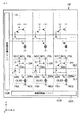
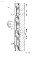
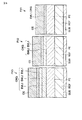
図1は、本発明の一態様に係る有機EL表示装置を概略的に示す平面図である。図2は、図1の表示装置に採用可能な構造の一例を概略的に示す断面図である。図3は、図2の表示装置が含む有機EL素子に採用可能な構造の一例を概略的に示す断面図である。図4は、図2の表示装置で採用可能な発光層の配置の一例を概略的に示す平面図である。 FIG. 1 is a plan view schematically showing an organic EL display device according to an aspect of the present invention. FIG. 2 is a cross-sectional view schematically showing an example of a structure that can be employed in the display device of FIG. FIG. 3 is a cross-sectional view schematically showing an example of a structure that can be employed in the organic EL element included in the display device of FIG. FIG. 4 is a plan view schematically showing an example of the arrangement of the light emitting layers that can be employed in the display device of FIG.
図1及び図2の表示装置は、アクティブマトリクス型駆動方式を採用した上面発光型の有機EL表示装置である。この表示装置は、表示パネルDPと、映像信号線ドライバXDRと、走査信号線ドライバYDRとを含んでいる。 The display device of FIGS. 1 and 2 is a top emission type organic EL display device adopting an active matrix driving method. This display device includes a display panel DP, a video signal line driver XDR, and a scanning signal line driver YDR.
表示パネルDPは、図1及び図2に示すように、例えば、ガラス基板などの絶縁基板SUBを含んでいる。基板SUB上には、図示しないアンダーコート層が形成されている。アンダーコート層は、例えば、基板SUB上にSiNx層とSiOx層とをこの順に積層してなる。 As illustrated in FIGS. 1 and 2, the display panel DP includes an insulating substrate SUB such as a glass substrate, for example. An undercoat layer (not shown) is formed on the substrate SUB. The undercoat layer is formed, for example, by laminating a SiN x layer and a SiO x layer in this order on the substrate SUB.
アンダーコート層上には、例えば不純物を含有したポリシリコンからなる半導体パターンが形成されている。この半導体パターンの一部は、図2の半導体層SCとして利用している。半導体層SCには、ソース及びドレインとして利用する不純物拡散領域が形成されている。また、この半導体パターンの他の一部は、後述するキャパシタCの下部電極として利用している。下部電極は、後述する画素PX1乃至PX3に対応して配列している。 On the undercoat layer, for example, a semiconductor pattern made of polysilicon containing impurities is formed. A part of this semiconductor pattern is used as the semiconductor layer SC of FIG. Impurity diffusion regions used as a source and a drain are formed in the semiconductor layer SC. Further, another part of the semiconductor pattern is used as a lower electrode of a capacitor C described later. The lower electrodes are arranged corresponding to pixels PX1 to PX3 described later.
なお、画素PX1乃至PX3は、この順にX方向に並んでおり、トリプレットを構成している。表示領域内では、このトリプレットがX方向とY方向とに配列している。すなわち、表示領域内では、画素PX1をY方向に並べてなる画素列と、画素PX2をY方向に並べてなる画素列と、画素PX3をY方向に並べてなる画素列とがこの順にX方向に並べられ、さらに、これら3つの画素列がX方向に繰り返し並べられている。 Note that the pixels PX1 to PX3 are arranged in this order in the X direction to form a triplet. In the display area, the triplets are arranged in the X direction and the Y direction. That is, in the display area, a pixel column in which the pixels PX1 are arranged in the Y direction, a pixel column in which the pixels PX2 are arranged in the Y direction, and a pixel column in which the pixels PX3 are arranged in the Y direction are arranged in this order in the X direction. In addition, these three pixel columns are repeatedly arranged in the X direction.
半導体パターンは、図2に示すゲート絶縁膜GIで被覆されている。ゲート絶縁膜GIは、例えばTEOS(tetraethyl orthosilicate)などを用いて形成することができる。 The semiconductor pattern is covered with the gate insulating film GI shown in FIG. The gate insulating film GI can be formed using, for example, TEOS (tetraethyl orthosilicate).
ゲート絶縁膜GI上には、図1に示す走査信号線SL1及びSL2が形成されている。走査信号線SL1及びSL2は、各々がX方向に延びており、Y方向に交互に配列している。走査信号線SL1及びSL2は、例えばMoWなどからなる。 On the gate insulating film GI, the scanning signal lines SL1 and SL2 shown in FIG. 1 are formed. The scanning signal lines SL1 and SL2 each extend in the X direction and are alternately arranged in the Y direction. The scanning signal lines SL1 and SL2 are made of, for example, MoW.
ゲート絶縁膜GI上には、キャパシタCの上部電極がさらに配置されている。上部電極は、画素PX1乃至PX3に対応して配列しており、下部電極と向き合っている。上部電極は、例えばMoWなどからなり、走査信号線SL1及びSL2と同一の工程で形成することができる。 An upper electrode of the capacitor C is further disposed on the gate insulating film GI. The upper electrode is arranged corresponding to the pixels PX1 to PX3, and faces the lower electrode. The upper electrode is made of, for example, MoW and can be formed in the same process as the scanning signal lines SL1 and SL2.
走査信号線SL1及びSL2は、半導体層SCと交差している。走査信号線SL1と半導体層SCとの交差部は図1及び図2に示すスイッチングトランジスタSWaを構成しており、走査信号線SL2と半導体層SCとの交差部は図1に示すスイッチングトランジスタSWb及びSWcを構成している。また、下部電極と上部電極とそれらの間に介在した絶縁膜GIとは図1に示すキャパシタCを構成している。上部電極は半導体層SCと交差した延長部を含んでおり、延長部と半導体層SCとの交差部は図1に示す駆動トランジスタDRを構成している。 The scanning signal lines SL1 and SL2 intersect the semiconductor layer SC. The intersection of the scanning signal line SL1 and the semiconductor layer SC constitutes the switching transistor SWa shown in FIGS. 1 and 2, and the intersection of the scanning signal line SL2 and the semiconductor layer SC is the switching transistor SWb shown in FIG. SWc is configured. Moreover, the lower electrode, the upper electrode, and the insulating film GI interposed therebetween constitute the capacitor C shown in FIG. The upper electrode includes an extension that intersects with the semiconductor layer SC, and the intersection between the extension and the semiconductor layer SC forms the drive transistor DR shown in FIG.
なお、この例では、駆動トランジスタDR及びスイッチングトランジスタSWa乃至SWcは、トップゲート型のpチャネル薄膜トランジスタである。また、図2に参照符号Gで示す部分は、スイッチングトランジスタSWaのゲートである。 In this example, the drive transistor DR and the switching transistors SWa to SWc are top-gate p-channel thin film transistors. Further, the portion indicated by reference numeral G in FIG. 2 is the gate of the switching transistor SWa.
ゲート絶縁膜GI、走査信号線SL1及びSL2、並びに上部電極は、図2に示す層間絶縁膜IIで被覆されている。層間絶縁膜IIは、例えばプラズマCVD(chemical vapor deposition)法により堆積させたSiOxなどからなる。 The gate insulating film GI, the scanning signal lines SL1 and SL2, and the upper electrode are covered with an interlayer insulating film II shown in FIG. The interlayer insulating film II is made of, for example, SiO x deposited by plasma CVD (chemical vapor deposition).
層間絶縁膜II上には、図1に示す映像信号線DLと電源線PSLとが形成されている。映像信号線DLは、図1に示すように、各々がY方向に延びており、X方向に配列している。電源線PSLは、例えば、各々がY方向に延びており、X方向に配列している。 On the interlayer insulating film II, the video signal line DL and the power supply line PSL shown in FIG. 1 are formed. As shown in FIG. 1, each video signal line DL extends in the Y direction and is arranged in the X direction. For example, each of the power supply lines PSL extends in the Y direction and is arranged in the X direction.
層間絶縁膜II上には、図2に示すソース電極SE及びドレイン電極DEがさらに形成されている。ソース電極SE及びドレイン電極DEは、画素PX1乃至PX3の各々において素子同士を接続している。 On the interlayer insulating film II, the source electrode SE and the drain electrode DE shown in FIG. 2 are further formed. The source electrode SE and the drain electrode DE connect elements in each of the pixels PX1 to PX3.
また、ソース電極SEとドレイン電極DEは、層間絶縁膜IIに空けられたコンタクトホールにより、半導体層SCに設けられた不純物拡散領域に接続されている。 The source electrode SE and the drain electrode DE are connected to an impurity diffusion region provided in the semiconductor layer SC by a contact hole opened in the interlayer insulating film II.
映像信号線DLと電源線PSLとソース電極SEとドレイン電極DEとは、例えば、Mo/Al/Moの三層構造を有している。これらは、同一工程で形成可能である。 The video signal line DL, the power supply line PSL, the source electrode SE, and the drain electrode DE have, for example, a three-layer structure of Mo / Al / Mo. These can be formed in the same process.
映像信号線DLと電源線PSLとソース電極SEとドレイン電極DEとは、図2に示すパッシベーション膜PSで被覆されている。パッシベーション膜PSは、例えばSiNxなどからなる。 The video signal line DL, the power supply line PSL, the source electrode SE, and the drain electrode DE are covered with a passivation film PS shown in FIG. The passivation film PS is made of, for example, SiN x .
パッシベーション膜PS上では、図2に示す画素電極PEが、画素PX1乃至PX3に対応して配列している。各画素電極PEは、パッシベーション膜PSに設けたコンタクトホールを介してドレイン電極DEに接続されており、このドレイン電極はスイッチングトランジスタSWaのドレインに接続されている。 On the passivation film PS, the pixel electrodes PE shown in FIG. 2 are arranged corresponding to the pixels PX1 to PX3. Each pixel electrode PE is connected to the drain electrode DE through a contact hole provided in the passivation film PS, and this drain electrode is connected to the drain of the switching transistor SWa.
画素電極PEは、この例では背面電極である。また、画素電極PEは、この例では陽極である。画素電極PEの材料としては、例えば、ITO(indium tin oxide)などの透明導電性酸化物を使用することができる。この場合、典型的には、図3に示すように、画素電極PEと基板SUBとの間に、例えばアルミニウムなどの金属材料からなる反射層REFを配置する。 The pixel electrode PE is a back electrode in this example. Further, the pixel electrode PE is an anode in this example. As a material of the pixel electrode PE, for example, a transparent conductive oxide such as ITO (indium tin oxide) can be used. In this case, typically, as shown in FIG. 3, a reflective layer REF made of a metal material such as aluminum is disposed between the pixel electrode PE and the substrate SUB.
パッシベーション膜PS上には、さらに、図2に示す隔壁絶縁層PIが形成されている。隔壁絶縁層PIには、画素電極PEに対応した位置に貫通孔が設けられているか、或いは、画素電極PEが形成する列に対応した位置にスリットが設けられている。ここでは、一例として、隔壁絶縁層PIには、画素電極PEに対応した位置に貫通孔が設けられていることとする。 A partition insulating layer PI shown in FIG. 2 is further formed on the passivation film PS. In the partition insulating layer PI, a through hole is provided at a position corresponding to the pixel electrode PE, or a slit is provided at a position corresponding to a column formed by the pixel electrode PE. Here, as an example, the partition insulating layer PI is provided with a through hole at a position corresponding to the pixel electrode PE.
隔壁絶縁層PIは、例えば、有機絶縁層である。隔壁絶縁層PIは、例えば、フォトリソグラフィ技術を用いて形成することができる。 The partition insulating layer PI is, for example, an organic insulating layer. The partition insulating layer PI can be formed using, for example, a photolithography technique.
各画素電極PE上には、有機物層ORGが形成されている。有機物層ORGは、典型的には、図2に示すように、全ての画素PX1乃至PX3を含む表示領域に亘って広がった連続膜である。すなわち、典型的には、有機物層ORGは画素電極PEと隔壁絶縁層PIとを被覆している。 An organic layer ORG is formed on each pixel electrode PE. As shown in FIG. 2, the organic layer ORG is typically a continuous film extending over the display area including all the pixels PX1 to PX3. That is, typically, the organic layer ORG covers the pixel electrode PE and the partition insulating layer PI.
図3に示すように、有機物層ORGのうち、画素PX1の画素電極PEに対応した部分は、発光層EML1を含んでいる。有機物層ORGのうち、画素PX1の画素電極PEに対応した部分は、画素電極PEと発光層EML1との間に正孔輸送層HTLをさらに含むことができる。また、有機物層ORGのうち、画素PX1の画素電極PEに対応した部分は、発光層EML1と後述する対向電極CEとの間に電子輸送層ETLをさらに含むことができる。 As shown in FIG. 3, a portion of the organic layer ORG corresponding to the pixel electrode PE of the pixel PX1 includes a light emitting layer EML1. A portion of the organic layer ORG corresponding to the pixel electrode PE of the pixel PX1 may further include a hole transport layer HTL between the pixel electrode PE and the light emitting layer EML1. In addition, a portion of the organic layer ORG corresponding to the pixel electrode PE of the pixel PX1 can further include an electron transport layer ETL between the light emitting layer EML1 and a counter electrode CE described later.
有機物層ORGのうち、画素PX2の画素電極PEに対応した部分は、発光層EML1と発光層EML2とを含んでいる。発光層EML2は、画素電極PEと発光層EML1との間に介在している。有機物層ORGのうち、画素PX2の画素電極PEに対応した部分は、画素電極PEと発光層EML2との間に正孔輸送層HTLをさらに含むことができる。また、有機物層ORGのうち、画素PX2の画素電極PEに対応した部分は、発光層EML1と対向電極CEとの間に電子輸送層ETLをさらに含むことができる。 A portion of the organic layer ORG corresponding to the pixel electrode PE of the pixel PX2 includes a light emitting layer EML1 and a light emitting layer EML2. The light emitting layer EML2 is interposed between the pixel electrode PE and the light emitting layer EML1. A portion of the organic layer ORG corresponding to the pixel electrode PE of the pixel PX2 may further include a hole transport layer HTL between the pixel electrode PE and the light emitting layer EML2. In addition, a portion of the organic layer ORG corresponding to the pixel electrode PE of the pixel PX2 may further include an electron transport layer ETL between the light emitting layer EML1 and the counter electrode CE.
有機物層ORGのうち、画素PX3の画素電極PEに対応した部分は、発光層EML1と発光層EML3とを含んでいる。発光層EML3は、画素電極PEと発光層EML1との間に介在している。有機物層ORGのうち、画素PX3の画素電極PEに対応した部分は、画素電極PEと発光層EML3との間に正孔輸送層HTLをさらに含むことができる。また、有機物層ORGのうち、画素PX3の画素電極PEに対応した部分は、発光層EML1と対向電極CEとの間に電子輸送層ETLをさらに含むことができる。 A portion of the organic layer ORG corresponding to the pixel electrode PE of the pixel PX3 includes a light emitting layer EML1 and a light emitting layer EML3. The light emitting layer EML3 is interposed between the pixel electrode PE and the light emitting layer EML1. A portion of the organic layer ORG corresponding to the pixel electrode PE of the pixel PX3 may further include a hole transport layer HTL between the pixel electrode PE and the light emitting layer EML3. In addition, a portion of the organic layer ORG corresponding to the pixel electrode PE of the pixel PX3 may further include an electron transport layer ETL between the light emitting layer EML1 and the counter electrode CE.
発光層EML1は、発光色が青色のルミネセンス性有機化合物又は組成物を含んだ薄膜である。発光層EML1は、例えば、ホスト材料とドーパント材料との混合物からなる。発光層EML1は、例えば、画素PX1乃至PX3に対応してX方向とY方向とに配列している。或いは、発光層EML1は、Y方向に延びた帯形状を有しており、画素PX1乃至PX3の列に対応してX方向に配列している。或いは、発光層EML1は、図4に示すように、全ての画素PX1乃至PX3を含む表示領域に亘って広がった連続膜である。一例として、発光層EML1は連続膜であるとする。 The light emitting layer EML1 is a thin film containing a luminescent organic compound or composition whose emission color is blue. The light emitting layer EML1 is made of, for example, a mixture of a host material and a dopant material. For example, the light emitting layer EML1 is arranged in the X direction and the Y direction corresponding to the pixels PX1 to PX3. Alternatively, the light emitting layer EML1 has a band shape extending in the Y direction, and is arranged in the X direction corresponding to the columns of the pixels PX1 to PX3. Alternatively, as shown in FIG. 4, the light emitting layer EML1 is a continuous film extending over the display area including all the pixels PX1 to PX3. As an example, the light emitting layer EML1 is assumed to be a continuous film.
発光層EML2は、発光色が緑色のルミネセンス性有機化合物又は組成物を含んだ薄膜である。発光層EML2は、例えば、ホスト材料とドーパント材料との混合物からなる。発光層EML2は、例えば、画素PX2に対応してX方向とY方向とに配列している。或いは、発光層EML2は、図4に示すように、Y方向に延びた帯形状を有しており、画素PX2の列に対応してX方向に配列している。一例として、発光層EML2は、後者の構造を有しているとする。 The light emitting layer EML2 is a thin film containing a luminescent organic compound or composition whose emission color is green. The light emitting layer EML2 is made of, for example, a mixture of a host material and a dopant material. For example, the light emitting layer EML2 is arranged in the X direction and the Y direction corresponding to the pixel PX2. Alternatively, as shown in FIG. 4, the light emitting layer EML2 has a band shape extending in the Y direction, and is arranged in the X direction corresponding to the column of the pixels PX2. As an example, the light emitting layer EML2 is assumed to have the latter structure.
発光層EML3は、発光色が赤色のルミネセンス性有機化合物又は組成物を含んだ薄膜である。発光層EML3は、例えば、ホスト材料とドーパント材料との混合物からなる。発光層EML3は、例えば、画素PX3に対応してX方向とY方向とに配列している。或いは、発光層EML3は、図4に示すように、Y方向に延びた帯形状を有しており、画素PX1の列に対応してX方向に配列している。一例として、発光層EML3は、後者の構造を有しているとする。 The light emitting layer EML3 is a thin film containing a luminescent organic compound or composition whose emission color is red. The light emitting layer EML3 is made of, for example, a mixture of a host material and a dopant material. For example, the light emitting layer EML3 is arranged in the X direction and the Y direction corresponding to the pixel PX3. Alternatively, as shown in FIG. 4, the light emitting layer EML3 has a band shape extending in the Y direction, and is arranged in the X direction corresponding to the column of the pixels PX1. As an example, it is assumed that the light emitting layer EML3 has the latter structure.
なお、波長が400nm乃至435nmの範囲内にある光の色を紫、波長が435nm乃至480nmの範囲内にある光の色を青、波長が480nm乃至490nmの範囲内にある光の色を緑青、波長が490nm乃至500nmの範囲内にある光の色を青緑、波長が500nm乃至560nmの範囲内にある光の色を緑、波長が560nm乃至580nmの範囲内にある光の色を黄緑、波長が580nm乃至595nmの範囲内にある光の色を黄、波長が595nm乃至610nmの範囲内にある光の色を橙、波長が610nm乃至750nmの範囲内にある光の色を赤、波長が750nm乃至800nmの範囲内にある光の色を赤紫と定義するのが一般的である。ここでは、主波長が400nm乃至490nmの範囲内にある光の色を青色、主波長が490nmより長く且つ595nmよりも短い光の色を緑色、主波長が595nm乃至800nmの範囲内にある光の色を赤色と定義する。 Note that the color of light having a wavelength in the range of 400 nm to 435 nm is purple, the color of light having a wavelength in the range of 435 nm to 480 nm is blue, the color of light having a wavelength in the range of 480 nm to 490 nm is patina, The color of light with a wavelength in the range of 490 nm to 500 nm is blue-green, the color of light with a wavelength in the range of 500 nm to 560 nm is green, the color of light with a wavelength in the range of 560 nm to 580 nm is yellow-green, The color of light having a wavelength in the range of 580 nm to 595 nm is yellow, the color of light having a wavelength in the range of 595 nm to 610 nm is orange, the color of light having a wavelength in the range of 610 nm to 750 nm is red, and the wavelength is Generally, the color of light in the range of 750 nm to 800 nm is defined as magenta. Here, the color of light having a dominant wavelength in the range of 400 nm to 490 nm is blue, the color of light having a dominant wavelength longer than 490 nm and shorter than 595 nm is green, and the light having a dominant wavelength in the range of 595 nm to 800 nm. The color is defined as red.
正孔輸送層HTL及び電子輸送層ETLは、典型的には、表示領域に亘って広がった連続膜である。正孔輸送層HTL及び電子輸送層ETLは、例えば、画素PX1乃至PX3に対応して或いはそれらの行又は列に対応してパターニングされていてもよい。 The hole transport layer HTL and the electron transport layer ETL are typically continuous films extending over the display region. The hole transport layer HTL and the electron transport layer ETL may be patterned, for example, corresponding to the pixels PX1 to PX3 or corresponding to their rows or columns.
有機物層ORGは、正孔輸送層HTLと発光層EML1との間、正孔輸送層HTLと発光層EML2との間、正孔輸送層HTLと発光層EML3との間に、電子ブロッキング層をさらに含むことができる。また、有機物層ORGは、発光層EML3と電子輸送層ETLとの間に、正孔ブロッキング層をさらに含むことができる。電子ブロッキング層及び正孔ブロッキング層は、典型的には、表示領域に亘って広がった連続膜である。電子ブロッキング層及び正孔ブロッキング層は、例えば、画素PX1乃至PX3に対応して或いはそれらの行又は列に対応してパターニングされていてもよい。 The organic layer ORG further includes an electron blocking layer between the hole transport layer HTL and the light emitting layer EML1, between the hole transport layer HTL and the light emitting layer EML2, and between the hole transport layer HTL and the light emitting layer EML3. Can be included. The organic layer ORG may further include a hole blocking layer between the light emitting layer EML3 and the electron transport layer ETL. The electron blocking layer and the hole blocking layer are typically continuous films extending over the display region. The electron blocking layer and the hole blocking layer may be patterned, for example, corresponding to the pixels PX1 to PX3 or corresponding to their rows or columns.
隔壁絶縁層PI及び有機物層ORGは、対向電極CEで被覆されている。この例では、対向電極CEは、画素PX1乃至PX3で共用する共通電極である。また、この例では、対向電極CEは、陰極であり且つ光透過性の前面電極で、マグネシウムMgと銀Agの合金薄膜を使用する。対向電極CEは、例えば、パッシベーション膜PSと隔壁絶縁層PIとに設けられたコンタクトホールを介して、映像信号線DLと同一の層上に形成された電極配線(図示せず)に電気的に接続されている。 The partition insulating layer PI and the organic layer ORG are covered with the counter electrode CE. In this example, the counter electrode CE is a common electrode shared by the pixels PX1 to PX3. In this example, the counter electrode CE is a cathode and a light-transmitting front electrode, and an alloy thin film of magnesium Mg and silver Ag is used. The counter electrode CE is electrically connected to an electrode wiring (not shown) formed on the same layer as the video signal line DL through, for example, a contact hole provided in the passivation film PS and the partition insulating layer PI. It is connected.
画素電極PEと有機物層ORGと対向電極CEとは、画素電極PEに対応して配列した有機EL素子OLEDを形成している。なお、図4において、参照符号EA1乃至EA3は、画素PX1乃至PX3が含む有機EL素子OLEDの発光部をそれぞれ示している。発光部EA1乃至EA3の各々は、Y方向に延びた直角四辺形である。図4の構造では、発光部EA1乃至EA3の面積は、互いに等しい。 The pixel electrode PE, the organic layer ORG, and the counter electrode CE form an organic EL element OLED arranged in correspondence with the pixel electrode PE. In FIG. 4, reference numerals EA1 to EA3 indicate the light emitting portions of the organic EL elements OLED included in the pixels PX1 to PX3, respectively. Each of the light emitting units EA1 to EA3 is a right-angled quadrilateral extending in the Y direction. In the structure of FIG. 4, the areas of the light emitting portions EA1 to EA3 are equal to each other.
図3に示すように、各有機EL素子OLEDは、画素電極PEと有機物層ORGとの間に正孔注入層HILをさらに含むことができる。また、各有機EL素子OLEDは、有機物層ORGと対向電極CEとの間に電子注入層EILをさらに含むことができる。正孔注入層HIL及び電子注入層EILは、典型的には、表示領域に亘って広がった連続膜である。正孔注入層HIL及び電子注入層EILは、例えば、画素PX1乃至PX3に対応して或いはそれらの行又は列に対応してパターニングされていてもよい。 As shown in FIG. 3, each organic EL element OLED may further include a hole injection layer HIL between the pixel electrode PE and the organic layer ORG. Each organic EL element OLED can further include an electron injection layer EIL between the organic layer ORG and the counter electrode CE. The hole injection layer HIL and the electron injection layer EIL are typically continuous films extending over the display region. The hole injection layer HIL and the electron injection layer EIL may be patterned, for example, corresponding to the pixels PX1 to PX3 or corresponding to their rows or columns.
画素PX1乃至PX3の各々は、図1に示すように、駆動トランジスタDRと、スイッチングトランジスタSWa乃至SWcと、有機EL素子OLEDと、キャパシタCとを含んでいる。上記の通り、この例では、駆動トランジスタDR及びスイッチングトランジスタSWa乃至SWcはpチャネル薄膜トランジスタである。また、この例では、画素PX1が含む有機EL素子OLEDは青色に発光し、画素PX2が含む有機EL素子OLEDは緑色に発光し、画素PX3が含む有機EL素子OLEDは赤色に発光する。 As shown in FIG. 1, each of the pixels PX1 to PX3 includes a drive transistor DR, switching transistors SWa to SWc, an organic EL element OLED, and a capacitor C. As described above, in this example, the drive transistor DR and the switching transistors SWa to SWc are p-channel thin film transistors. In this example, the organic EL element OLED included in the pixel PX1 emits blue light, the organic EL element OLED included in the pixel PX2 emits green light, and the organic EL element OLED included in the pixel PX3 emits red light.
駆動トランジスタDRとスイッチングトランジスタSWaと有機EL素子OLEDとは、第1電源端子ND1と第2電源端子ND2との間で、この順に直列に接続されている。この例では、電源端子ND1は高電位電源端子であり、電源端子ND2は低電位電源端子である。 The drive transistor DR, the switching transistor SWa, and the organic EL element OLED are connected in series in this order between the first power supply terminal ND1 and the second power supply terminal ND2. In this example, the power supply terminal ND1 is a high potential power supply terminal, and the power supply terminal ND2 is a low potential power supply terminal.
スイッチングトランジスタSWaのゲートは、走査信号線SL1に接続されている。スイッチングトランジスタSWbは映像信号線DLと駆動トランジスタDRのドレインとの間に接続されており、そのゲートは走査信号線SL2に接続されている。スイッチングトランジスタSWcは駆動トランジスタDRのドレインとゲートとの間に接続されており、そのゲートは走査信号線SL2に接続されている。 The gate of the switching transistor SWa is connected to the scanning signal line SL1. The switching transistor SWb is connected between the video signal line DL and the drain of the drive transistor DR, and its gate is connected to the scanning signal line SL2. The switching transistor SWc is connected between the drain and gate of the driving transistor DR, and the gate is connected to the scanning signal line SL2.
キャパシタCは、駆動トランジスタDRのゲートと定電位端子ND1’との間に接続されている。この例では、定電位端子ND1’は、電源端子ND1に接続されている。 The capacitor C is connected between the gate of the driving transistor DR and the constant potential terminal ND1 '. In this example, the constant potential terminal ND1 'is connected to the power supply terminal ND1.
映像信号線ドライバXDR及び走査信号線ドライバYDRは、基板SUB上に配置されている。すなわち、映像信号線ドライバXDR及び走査信号線ドライバYDRは、COG(chip on glass)実装している。映像信号線ドライバXDR及び走査信号線ドライバYDRは、COG実装する代わりに、TCP(tape carrier package)実装してもよい。或いは、映像信号線ドライバXDR及び走査信号線ドライバYDRは、基板SUB上に形成してもよい。 The video signal line driver XDR and the scanning signal line driver YDR are disposed on the substrate SUB. That is, the video signal line driver XDR and the scanning signal line driver YDR are mounted on COG (chip on glass). The video signal line driver XDR and the scanning signal line driver YDR may be mounted by TCP (tape carrier package) instead of COG mounting. Alternatively, the video signal line driver XDR and the scanning signal line driver YDR may be formed on the substrate SUB.
映像信号線ドライバXDRには、映像信号線DLが接続されている。この例では、映像信号線ドライバXDRには、電源線PSLがさらに接続されている。映像信号線ドライバXDRは、映像信号線DLに映像信号として電流信号を出力するとともに、電源線PSLに電源電圧を供給する。 A video signal line DL is connected to the video signal line driver XDR. In this example, a power supply line PSL is further connected to the video signal line driver XDR. The video signal line driver XDR outputs a current signal as a video signal to the video signal line DL and supplies a power supply voltage to the power supply line PSL.
走査信号線ドライバYDRには、走査信号線SL1及びSL2が接続されている。走査信号線ドライバYDRは、走査信号線SL1及びSL2にそれぞれ第1及び第2走査信号として電圧信号を出力する。 Scanning signal lines SL1 and SL2 are connected to the scanning signal line driver YDR. The scanning signal line driver YDR outputs voltage signals as first and second scanning signals to the scanning signal lines SL1 and SL2, respectively.
この有機EL表示装置で画像を表示する場合、例えば、走査信号線SL2を順次走査する。すなわち、画素PX1乃至PX3を行毎に選択する。或る行を選択している選択期間では、その行が含む画素PX1乃至PX3に対して書込動作を行う。そして、その行を選択していない非選択期間では、その行が含む画素PX1乃至PX3で表示動作を行う。 When an image is displayed on this organic EL display device, for example, the scanning signal line SL2 is sequentially scanned. That is, the pixels PX1 to PX3 are selected for each row. In a selection period in which a certain row is selected, a writing operation is performed on the pixels PX1 to PX3 included in the row. In a non-selection period in which the row is not selected, display operation is performed on the pixels PX1 to PX3 included in the row.
或る行の画素PX1乃至PX3を選択する選択期間では、走査信号線ドライバYDRは、先の画素PX1乃至PX3が接続された走査信号線SL1にスイッチングトランジスタSWaを開く(非導通状態とする)走査信号を電圧信号として出力し、続いて、先の画素PX1乃至PX3が接続された走査信号線SL2にスイッチングトランジスタSWb及びSWcを閉じる(導通状態とする)走査信号を電圧信号として出力する。この状態で、映像信号線ドライバXDRは、映像信号線DLに映像信号を電流信号(書込電流)Isigとして出力し、駆動トランジスタDRのゲート−ソース間電圧Vgsを、先の映像信号Isigに対応した大きさに設定する。その後、走査信号線ドライバYDRは、先の画素PX1乃至PX3が接続された走査信号線SL2にスイッチングトランジスタSWb及びSWcを開く走査信号を電圧信号として出力し、続いて、先の画素PX1乃至PX3が接続された走査信号線SL1にスイッチングトランジスタSWaを閉じる走査信号を電圧信号として出力する。これにより、選択期間を終了する。 In the selection period in which the pixels PX1 to PX3 in a certain row are selected, the scanning signal line driver YDR performs scanning (opens a non-conducting state) to open the switching transistor SWa to the scanning signal line SL1 to which the previous pixels PX1 to PX3 are connected. The signal is output as a voltage signal, and subsequently, a scanning signal that closes the switching transistors SWb and SWc (sets the conductive state) to the scanning signal line SL2 to which the previous pixels PX1 to PX3 are connected is output as a voltage signal. In this state, the video signal line driver XDR outputs the video signal to the video signal line DL as a current signal (write current) I sig , and uses the gate-source voltage V gs of the drive transistor DR as the previous video signal I. Set the size corresponding to sig . Thereafter, the scanning signal line driver YDR outputs a scanning signal for opening the switching transistors SWb and SWc to the scanning signal line SL2 connected to the previous pixels PX1 to PX3 as a voltage signal, and then the previous pixels PX1 to PX3 A scanning signal for closing the switching transistor SWa is output as a voltage signal to the connected scanning signal line SL1. This ends the selection period.
選択期間に続く非選択期間では、スイッチングトランジスタSWaは閉じたままとし、スイッチングトランジスタSWb及びSWcは開いたままとする。非選択期間では、有機EL素子OLEDには、駆動トランジスタDRのゲート−ソース間電圧Vgsに対応した大きさの駆動電流Idrvが流れる。有機EL素子OLEDは、駆動電流Idrvの大きさに対応した輝度で発光する。ここで、Idrv≒Isigとなり、各画素で、電流信号(書込電流)Isigに対応した発光を得ることができる。 In the non-selection period following the selection period, the switching transistor SWa remains closed and the switching transistors SWb and SWc remain open. In the non-selection period, a drive current I drv having a magnitude corresponding to the gate-source voltage V gs of the drive transistor DR flows through the organic EL element OLED. The organic EL element OLED emits light with a luminance corresponding to the magnitude of the drive current I drv . Here, I drv ≈I sig , and light emission corresponding to the current signal (write current) I sig can be obtained in each pixel.
この有機EL表示装置は、例えば、以下の方法により製造することができる。
まず、先に説明した表示パネルDPから対向電極CEと電子注入層EILと有機物層ORGと正孔注入層HILとを除いた構造,すなわちアレイ基板,を準備する。
This organic EL display device can be manufactured, for example, by the following method.
First, a structure in which the counter electrode CE, the electron injection layer EIL, the organic material layer ORG, and the hole injection layer HIL are removed from the display panel DP described above, that is, an array substrate is prepared.
次に、画素電極PE上に、正孔注入層HILを形成する。正孔注入層HILは、例えば、表示領域に亘って広がった連続膜とする。 Next, a hole injection layer HIL is formed on the pixel electrode PE. The hole injection layer HIL is, for example, a continuous film extending over the display region.
次いで、正孔注入層HIL上に、有機物層ORGが含む各層を真空蒸着法によって形成する。発光層EML2及びEML3は、例えば、ファインマスクを用いた真空蒸着法により形成する。正孔注入層HILと正孔輸送層HTLと発光層EML1と電子輸送層ETLと電子注入層EILとは、例えば、ラフマスクを使用した真空蒸着法により形成する。 Next, each layer included in the organic layer ORG is formed on the hole injection layer HIL by a vacuum deposition method. The light emitting layers EML2 and EML3 are formed by, for example, a vacuum evaporation method using a fine mask. The hole injection layer HIL, the hole transport layer HTL, the light emitting layer EML1, the electron transport layer ETL, and the electron injection layer EIL are formed by, for example, a vacuum evaporation method using a rough mask.
なお、発光層EML2の形成に使用するファインマスクとしては、例えば、発光層EML2に対応して複数のスリットが形成されたものを使用する。また、発光層EML3の形成に使用するファインマスクとしては、例えば、発光層EML3に対応して複数のスリットが形成されたものを使用する。そして、先のラフマスクとしては、例えば、表示領域に対応した開口が形成されたものを使用する。 In addition, as a fine mask used for formation of the light emitting layer EML2, what used the some slit formed corresponding to the light emitting layer EML2 is used, for example. Moreover, as a fine mask used for formation of the light emitting layer EML3, for example, a mask in which a plurality of slits are formed corresponding to the light emitting layer EML3 is used. As the previous rough mask, for example, a mask having an opening corresponding to the display area is used.
その後、電子輸送層ETL上に、電子注入層EIL及び対向電極CEを順次形成する。さらに、有機EL素子OLEDを封止し、表示パネルDPに映像信号線ドライバXDRと走査信号線ドライバYDRとを実装する。以上のようにして、図1及び図2の有機EL表示装置を得る。 Thereafter, an electron injection layer EIL and a counter electrode CE are sequentially formed on the electron transport layer ETL. Further, the organic EL element OLED is sealed, and the video signal line driver XDR and the scanning signal line driver YDR are mounted on the display panel DP. As described above, the organic EL display device of FIGS. 1 and 2 is obtained.
ところで、1つの有機EL素子OLEDが発光層EML2又はEML3と発光層EML1とを含んでいると、発光層EML2又はEML3だけでなく、発光層EML1も発光する可能性がある。この場合、画素PX2又はPX3の発光色の純度が低下する。 By the way, when one organic EL element OLED includes the light emitting layer EML2 or EML3 and the light emitting layer EML1, not only the light emitting layer EML2 or EML3 but also the light emitting layer EML1 may emit light. In this case, the purity of the emission color of the pixel PX2 or PX3 is lowered.
これを防止するために、画素PX2の有機EL素子OLEDに、発光層EML1及びEML2のうち発光層EML2のみが発光する設計を採用する。同様に、画素PX3の有機EL素子OLEDには、発光層EML1及びEML3のうち発光層EML3のみが発光する設計を採用する。 In order to prevent this, a design in which only the light-emitting layer EML2 of the light-emitting layers EML1 and EML2 emits light is adopted for the organic EL element OLED of the pixel PX2. Similarly, the organic EL element OLED of the pixel PX3 adopts a design in which only the light emitting layer EML3 emits light among the light emitting layers EML1 and EML3.
例えば、電子輸送層ETLの電子移動度を、正孔輸送層HTLの正孔移動度と比較してより大きくする。そして、画素PX2の有機EL素子OLEDでは、電子輸送層ETLと発光層EML1との界面における電子に対する障壁を、正孔輸送層HTLと発光層EML2との界面における正孔の障壁と比較してより小さくする。また、画素PX3の有機EL素子OLEDでは、電子輸送層ETLと発光層EML1との界面における電子に対する障壁を、正孔輸送層HTLと発光層EML3との界面における正孔の障壁と比較してより小さくする。こうすると、画素PX2及びPX3において、発光層EML1が発光するのを抑制することができる。 For example, the electron mobility of the electron transport layer ETL is made larger than the hole mobility of the hole transport layer HTL. In the organic EL element OLED of the pixel PX2, the barrier against electrons at the interface between the electron transport layer ETL and the light emitting layer EML1 is more compared to the hole barrier at the interface between the hole transport layer HTL and the light emitting layer EML2. Make it smaller. Further, in the organic EL element OLED of the pixel PX3, the barrier against electrons at the interface between the electron transport layer ETL and the light emitting layer EML1 is more compared to the hole barrier at the interface between the hole transport layer HTL and the light emitting layer EML3. Make it smaller. In this way, the light emitting layer EML1 can be prevented from emitting light in the pixels PX2 and PX3.
上述した構造では、発光層EML1は発光色が青色のルミネセンス性有機化合物又は組成物を含み、発光層EML2及びEML3は発光色が緑及び赤色のルミネセンス性有機化合物又は組成物をそれぞれ含んでいる。 In the structure described above, the light emitting layer EML1 includes a luminescent organic compound or composition whose emission color is blue, and the light emission layers EML2 and EML3 include a luminescent organic compound or composition whose emission colors are green and red, respectively. Yes.
但し、発光色が赤色及び緑色のルミネセンス性有機化合物又は組成物は、それぞれ、青色光によって励起されて赤色及び緑色に発光することがある。それゆえ、上述した構造を採用した場合、画素PX2及びPX3の有機EL素子OLEDで発光層EML1が発光したとしても、画素PX2又はPX3の発光色の純度は低下し難い。 However, the luminescent organic compounds or compositions whose emission colors are red and green may be excited by blue light and emit red and green, respectively. Therefore, when the structure described above is employed, even if the light emitting layer EML1 emits light from the organic EL elements OLED of the pixels PX2 and PX3, the purity of the emission color of the pixel PX2 or PX3 is unlikely to decrease.
また、発光色が青色のルミネセンス性有機化合物又は組成物を含んだ薄膜を発光層EML1とした構造は、以下に説明するように、各有機EL素子OLEDに光共振器としての機能を与えるうえでも有利である。 In addition, the structure in which the thin film containing a luminescent organic compound or composition having a blue emission color is used as the light emitting layer EML1 provides each organic EL element OLED with a function as an optical resonator as described below. But it is advantageous.
図3の構造では、画素電極PEと反射層REFとの界面及び電子輸送層ETLと電子注入層EILとの界面は、発光層EML1乃至EML3が放出する光の一部を反射する。それゆえ、反射層REFと電子注入層EILとの間の光路長を最適化すれば、有機EL素子OLED内で繰り返し反射干渉を生じさせること,すなわち、有機EL素子OLEDに光共振器としての機能を与えること,ができる。 In the structure of FIG. 3, the interface between the pixel electrode PE and the reflective layer REF and the interface between the electron transport layer ETL and the electron injection layer EIL reflect part of the light emitted from the light emitting layers EML1 to EML3. Therefore, if the optical path length between the reflective layer REF and the electron injection layer EIL is optimized, reflection interference is repeatedly generated in the organic EL element OLED, that is, the organic EL element OLED functions as an optical resonator. Can be given.
光共振器の共振波長は、有機EL素子OLEDに要求される発光色に基づいて定める。換言すれば、先の光路長は、有機EL素子OLEDに要求される発光色に基づいて定める。典型的には、発光色が緑色の有機EL素子OLEDでは、発光色が青色の有機EL素子OLEDと比較して先の光路長をより長くし、発光色が赤色の有機EL素子OLEDでは、発光色が緑青色の有機EL素子OLEDと比較して先の光路長をより長くする。 The resonance wavelength of the optical resonator is determined based on the emission color required for the organic EL element OLED. In other words, the previous optical path length is determined based on the emission color required for the organic EL element OLED. Typically, the organic EL element OLED having a green emission color has a longer optical path length than the organic EL element OLED having a blue emission color, and the organic EL element OLED having a red emission color emits light. The previous optical path length is made longer than that of the organic EL element OLED whose color is green-blue.
図3から明らかなように、画素PX1の有機EL素子OLEDでは、画素PX2及び画素PX3の有機EL素子OLEDと比較して、先の光路長がより短い。それゆえ、発光色が青色のルミネセンス性有機化合物又は組成物を含んだ薄膜を発光層EML1とした構造を採用すると、工程数の増加を伴うことなく、各有機EL素子OLEDに光共振器としての機能を与えることができる。 As is apparent from FIG. 3, the organic EL element OLED of the pixel PX1 has a shorter optical path length than the organic EL elements OLED of the pixels PX2 and PX3. Therefore, when a thin film containing a luminescent organic compound or composition having a blue emission color is used as the light emitting layer EML1, each organic EL element OLED can be used as an optical resonator without increasing the number of steps. Can be given functions.
また、画素PX2の有機EL素子OLEDが発光層EML1乃至EML3のうち発光層EML2のみを含み且つ画素PX3の有機EL素子OLEDが発光層EML1乃至EML3のうち発光層EML3のみを含んでいる場合、各有機EL素子OLEDに光共振器としての機能を与えるためには、発光層EML2及びEML3をより厚く形成しなければならない。すなわち、この場合、発光層EML2及びEML3を形成するために、より多くの蒸発材料が必要である。これに対し、図3の構造では、画素PX2の有機EL素子OLEDは発光層EML1及びEML2を含み、画素PX3の有機EL素子OLEDは発光層EML1及びEML3を含んでいる。すなわち、これら有機EL素子OLEDは、複数の発光層を含んでいる。そのため、この構造を採用すると、発光層EML2及びEML3を形成するための蒸発材料の使用量を低減することができる。 Further, when the organic EL element OLED of the pixel PX2 includes only the light emitting layer EML2 among the light emitting layers EML1 to EML3 and the organic EL element OLED of the pixel PX3 includes only the light emitting layer EML3 among the light emitting layers EML1 to EML3, In order to give the organic EL element OLED a function as an optical resonator, the light emitting layers EML2 and EML3 must be formed thicker. That is, in this case, more evaporation material is required to form the light emitting layers EML2 and EML3. On the other hand, in the structure of FIG. 3, the organic EL element OLED of the pixel PX2 includes the light emitting layers EML1 and EML2, and the organic EL element OLED of the pixel PX3 includes the light emitting layers EML1 and EML3. That is, these organic EL elements OLED include a plurality of light emitting layers. Therefore, when this structure is employed, the amount of evaporation material used for forming the light emitting layers EML2 and EML3 can be reduced.
図3の構造では、発光層EML2の厚さと発光層EML3の厚さとは等しいが、それらは異なっていてもよい。 In the structure of FIG. 3, the thickness of the light emitting layer EML2 and the thickness of the light emitting layer EML3 are equal, but they may be different.
図5は、図2の表示装置が含む有機EL素子に採用可能な構造の他の例を概略的に示す断面図である。この構造では、発光層EML3は、発光層EML2と比較してより厚い。それゆえ、画素PX3の有機EL素子OLEDでは、画素PX2の有機EL素子OLEDと比較して、先の光路長がより長い。この構造を採用すると、各有機EL素子OLEDに光共振器としての機能を与えるうえで、設計の自由度がより大きくなる。 FIG. 5 is a cross-sectional view schematically showing another example of a structure that can be employed in the organic EL element included in the display device of FIG. In this structure, the light emitting layer EML3 is thicker than the light emitting layer EML2. Therefore, the organic EL element OLED of the pixel PX3 has a longer optical path length than the organic EL element OLED of the pixel PX2. When this structure is employed, the degree of freedom in design is further increased in providing each organic EL element OLED with a function as an optical resonator.
図3の構造では、画素PX3は発光層EML2を含んでいないが、画素PX3は発光層EML2をさらに含んでいてもよい。 In the structure of FIG. 3, the pixel PX3 does not include the light emitting layer EML2, but the pixel PX3 may further include the light emitting layer EML2.
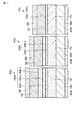
図6は、図2の表示装置が含む有機EL素子に採用可能な構造の他の例を概略的に示す断面図である。図7は、有機EL素子に図6の構造を採用した場合に、図2の表示装置で採用可能な発光層の配置の一例を概略的に示す平面図である。 FIG. 6 is a cross-sectional view schematically showing another example of a structure that can be employed in the organic EL element included in the display device of FIG. FIG. 7 is a plan view schematically showing an example of the arrangement of the light emitting layers that can be adopted in the display device of FIG. 2 when the structure of FIG. 6 is adopted in the organic EL element.
図6の構造では、画素PX3の有機EL素子OLEDは、発光層EML1と発光層EML3との間に発光層EML2をさらに含んでいる。この構造を採用すると、各有機EL素子OLEDに光共振器としての機能を与えるうえで、設計の自由度がより大きくなる。 In the structure of FIG. 6, the organic EL element OLED of the pixel PX3 further includes a light emitting layer EML2 between the light emitting layer EML1 and the light emitting layer EML3. When this structure is employed, the degree of freedom in design is further increased in providing each organic EL element OLED with a function as an optical resonator.
そして、図6の構造では、画素PX2及びPX3の有機EL素子OLEDは、複数の発光層を含んでいる。そのため、この構造を採用すると、図3の構造を採用した場合と同様、発光層EML2及びEML3を形成するための蒸発材料の使用量を低減することができる。 In the structure of FIG. 6, the organic EL elements OLED of the pixels PX2 and PX3 include a plurality of light emitting layers. Therefore, when this structure is adopted, the amount of the evaporation material used for forming the light emitting layers EML2 and EML3 can be reduced as in the case where the structure of FIG. 3 is adopted.
また、図6の構造を採用した場合、隣接した画素PX2及びPX3間で発光層EML2を繋げることができる。したがって、例えば、発光層EML2は、図7に示すように、互いに隣接した画素PX2と画素PX3との組が形成する列と向き合うようにパターニングされたストライプパターンとすることができる。 When the structure of FIG. 6 is adopted, the light emitting layer EML2 can be connected between the adjacent pixels PX2 and PX3. Therefore, for example, as shown in FIG. 7, the light-emitting layer EML2 can be a stripe pattern that is patterned so as to face a column formed by a pair of adjacent pixels PX2 and PX3.
図6の構造には、様々な変形が可能である。以下、これについて説明する。
図8は、図6の構造の一変形例を示す断面図である。図8の構造は、図6の構造から正孔注入層HILと正孔輸送層HTLと電子注入層EILと電子輸送層ETLとを省略したものに相当している。
Various modifications can be made to the structure of FIG. This will be described below.
FIG. 8 is a cross-sectional view showing a modification of the structure of FIG. The structure in FIG. 8 corresponds to a structure in which the hole injection layer HIL, the hole transport layer HTL, the electron injection layer EIL, and the electron transport layer ETL are omitted from the structure in FIG.
この構造を採用した場合、例えば、対向電極CEと発光層EML1との界面における電子の障壁を、画素電極PEと発光層EML1乃至EML3の各々との界面における正孔の障壁と比較してより小さくする。すなわち、対向電極CEから有機物層ORGへの電子の注入を生じさせるために電極PE及びCE間に印加すべき順方向バイアスの最小値を、画素電極PEから有機物層ORGへの正孔の注入を生じさせるために電極PE及びCE間に印加すべき順方向バイアスの最小値と比較してより小さくする。或いは、発光層EML2の正孔移動度をその電子移動度よりも小さくし、発光層EML3の正孔移動度をその電子移動度よりも小さくする。或いは、これら設計の双方を採用する。 When this structure is adopted, for example, the electron barrier at the interface between the counter electrode CE and the light emitting layer EML1 is smaller than the hole barrier at the interface between the pixel electrode PE and each of the light emitting layers EML1 to EML3. To do. That is, the minimum value of the forward bias to be applied between the electrodes PE and CE in order to cause the injection of electrons from the counter electrode CE to the organic layer ORG, and the injection of holes from the pixel electrode PE to the organic layer ORG. It is made smaller compared to the minimum value of the forward bias to be applied between the electrodes PE and CE in order to generate. Alternatively, the hole mobility of the light emitting layer EML2 is made smaller than its electron mobility, and the hole mobility of the light emitting layer EML3 is made smaller than its electron mobility. Alternatively, both of these designs are adopted.
こうすると、例えば、画素PX2では、発光層EML1と比較して発光層EML2において励起子の密度をより高くすることができ、画素PX3では、発光層EML1及びEML2と比較して発光層EML3において励起子の密度をより高くすることができる。したがって、画素PX2において発光層EML1が発光するのを抑制できると共に、画素PX3において発光層EML1及びEML2が発光するのを抑制できる。なお、発光層EML1乃至EML3の電子移動度は、例えば、ドーパント濃度を低くすると大きくなり、ドーパント濃度を高めると小さくなる。 Thus, for example, in the pixel PX2, the density of excitons can be increased in the light emitting layer EML2 compared to the light emitting layer EML1, and in the pixel PX3, excitation in the light emitting layer EML3 compared to the light emitting layers EML1 and EML2. The density of the child can be increased. Therefore, the light emitting layer EML1 can be prevented from emitting light in the pixel PX2, and the light emitting layers EML1 and EML2 can be prevented from emitting light in the pixel PX3. The electron mobility of the light emitting layers EML1 to EML3 increases, for example, when the dopant concentration is lowered, and decreases when the dopant concentration is increased.
図9は、図6の構造の他の変形例を示す断面図である。図9の構造は、発光層EML1乃至EML3の積層順を逆にしたこと以外は図8の構造と同様である。 FIG. 9 is a cross-sectional view showing another modification of the structure of FIG. The structure in FIG. 9 is the same as the structure in FIG. 8 except that the stacking order of the light emitting layers EML1 to EML3 is reversed.
この構造を採用した場合、例えば、画素電極PEと発光層EML1との界面における正孔の障壁を、対向電極CEと発光層EML1乃至EML3との界面における電子の障壁と比較してより小さくする。或いは、発光層EML1の正孔移動度をその電子移動度よりも大きくし、発光層EML2の正孔移動度をその電子移動度よりも大きくする。或いは、これら設計の双方を採用する。こうすると、画素PX2において発光層EML1が発光するのを抑制できると共に、画素PX3において発光層EML1及びEML2が発光するのを抑制できる。 When this structure is adopted, for example, the hole barrier at the interface between the pixel electrode PE and the light emitting layer EML1 is made smaller than the electron barrier at the interface between the counter electrode CE and the light emitting layers EML1 to EML3. Alternatively, the hole mobility of the light emitting layer EML1 is made larger than its electron mobility, and the hole mobility of the light emitting layer EML2 is made larger than its electron mobility. Alternatively, both of these designs are adopted. This can suppress the light emission layer EML1 from emitting light in the pixel PX2, and can suppress the light emission layers EML1 and EML2 from emitting light in the pixel PX3.
図10は、図6の構造の他の変形例を示す断面図である。図10の構造は、対向電極CEが光学マッチング層MCで被覆されていること以外は図8の構造と同様である。 FIG. 10 is a cross-sectional view showing another modification of the structure of FIG. The structure of FIG. 10 is the same as the structure of FIG. 8 except that the counter electrode CE is covered with the optical matching layer MC.
光学マッチング層MCは、光透過性の層であって、絶縁基板SUBと封止基板SUB2との間隙にある窒素などの気体層との光学的なマッチングを図る。光学マッチング層MCの屈折率は有機物層ORGの屈折率とほぼ等しい。例えば、光学マッチング層MCとしては、SiON層などの透明無機絶縁層、ITO層などの透明無機導電層、有機物層ORGが含んでいる層などの透明有機物層を使用することができる。光学マッチング層MCを使用すると、光取り出し効率を高めることができる。 The optical matching layer MC is a light-transmitting layer, and optically matches a gas layer such as nitrogen in the gap between the insulating substrate SUB and the sealing substrate SUB2. The refractive index of the optical matching layer MC is substantially equal to the refractive index of the organic layer ORG. For example, as the optical matching layer MC, a transparent inorganic insulating layer such as a SiON layer, a transparent inorganic conductive layer such as an ITO layer, or a transparent organic layer such as a layer included in the organic layer ORG can be used. When the optical matching layer MC is used, the light extraction efficiency can be increased.
図11は、図6の構造の他の変形例を示す断面図である。図11の構造は、対向電極CEが光学マッチング層MCで被覆されていること以外は図9の構造と同様である。 FIG. 11 is a cross-sectional view showing another modification of the structure of FIG. The structure of FIG. 11 is the same as the structure of FIG. 9 except that the counter electrode CE is covered with the optical matching layer MC.
図12は、図6の構造の他の変形例を示す断面図である。図12の構造は、正孔注入層HILと電子注入層EILとを省略し且つ対向電極CEを光学マッチング層MCで被覆したこと以外は図6の構造と同様である。 FIG. 12 is a cross-sectional view showing another modification of the structure of FIG. The structure of FIG. 12 is the same as the structure of FIG. 6 except that the hole injection layer HIL and the electron injection layer EIL are omitted and the counter electrode CE is covered with the optical matching layer MC.
この構造を採用した場合、例えば、対向電極CEから電子輸送層ETLへの電子の注入を生じさせるために電極PE及びCE間に印加すべき順方向バイアスの最小値を、画素電極PEから正孔輸送層HTLへの正孔の注入を生じさせるために電極PE及びCE間に印加すべき順方向バイアスの最小値と比較してより小さくする。或いは、電子輸送層ETLと発光層EML1との界面における電子に対する障壁を、正孔輸送層HTLと発光層EML1乃至EML3との界面における正孔の障壁と比較してより小さくする。或いは、正孔輸送層HTL及び電子輸送層ETLとの組み合わせとして、正孔輸送層HTLの正孔移動度が電子輸送層ETLの電子移動度と比較してより小さいものを使用する。或いは、発光層EML2の正孔移動度をその電子移動度よりも小さくし、発光層EML3の正孔移動度をその電子移動度よりも小さくする。或いは、これら設計の2以上を採用する。こうすると、画素PX2において発光層EML1が発光するのを抑制できると共に、画素PX3において発光層EML1及びEML2が発光するのを抑制できる。 When this structure is adopted, for example, the minimum value of the forward bias to be applied between the electrodes PE and CE in order to cause injection of electrons from the counter electrode CE to the electron transport layer ETL is determined from the pixel electrode PE to the hole. It is smaller than the minimum value of the forward bias to be applied between the electrodes PE and CE to cause the injection of holes into the transport layer HTL. Alternatively, the barrier against electrons at the interface between the electron transport layer ETL and the light emitting layer EML1 is made smaller than the hole barrier at the interface between the hole transport layer HTL and the light emitting layers EML1 to EML3. Alternatively, as a combination of the hole transport layer HTL and the electron transport layer ETL, a hole transport layer having a smaller hole mobility than that of the electron transport layer ETL is used. Alternatively, the hole mobility of the light emitting layer EML2 is made smaller than its electron mobility, and the hole mobility of the light emitting layer EML3 is made smaller than its electron mobility. Alternatively, two or more of these designs are employed. This can suppress the light emission layer EML1 from emitting light in the pixel PX2, and can suppress the light emission layers EML1 and EML2 from emitting light in the pixel PX3.
図13は、図6の構造の他の変形例を示す断面図である。図13の構造は、発光層EML1乃至EML3の積層順を逆にしたこと以外は図12の構造と同様である。 FIG. 13 is a cross-sectional view showing another modification of the structure of FIG. The structure of FIG. 13 is the same as the structure of FIG. 12 except that the stacking order of the light emitting layers EML1 to EML3 is reversed.
この構造を採用した場合、例えば、画素電極PEから正孔輸送層HTLへの正孔の注入を生じさせるために電極PE及びCE間に印加すべき順方向バイアスの最小値を、対向電極CEから電子輸送層ETLへの電子の注入を生じさせるために電極PE及びCE間に印加すべき順方向バイアスの最小値と比較してより小さくする。或いは、正孔輸送層HTLと発光層EML1との界面における正孔に対する障壁を、電子輸送層ETLと発光層EML1乃至EML3との界面における電子の障壁と比較してより小さくする。或いは、正孔輸送層HTL及び電子輸送層ETLとの組み合わせとして、電子輸送層ETLの電子移動度が正孔輸送層HTLの正孔移動度と比較してより小さいものを使用する。或いは、発光層EML1の正孔移動度をその電子移動度よりも大きくし、発光層EML2の正孔移動度をその電子移動度よりも大きくする。或いは、これら設計の2以上を採用する。こうすると、画素PX2において発光層EML1が発光するのを抑制できると共に、画素PX3において発光層EML1及びEML2が発光するのを抑制できる。 When this structure is adopted, for example, the minimum value of the forward bias to be applied between the electrodes PE and CE to cause the injection of holes from the pixel electrode PE to the hole transport layer HTL is determined from the counter electrode CE. It is smaller than the minimum value of the forward bias to be applied between the electrodes PE and CE in order to cause the injection of electrons into the electron transport layer ETL. Alternatively, the barrier against holes at the interface between the hole transport layer HTL and the light emitting layer EML1 is made smaller than the electron barrier at the interface between the electron transport layer ETL and the light emitting layers EML1 to EML3. Alternatively, as a combination of the hole transport layer HTL and the electron transport layer ETL, one having an electron mobility of the electron transport layer ETL smaller than that of the hole transport layer HTL is used. Alternatively, the hole mobility of the light emitting layer EML1 is made larger than its electron mobility, and the hole mobility of the light emitting layer EML2 is made larger than its electron mobility. Alternatively, two or more of these designs are employed. This can suppress the light emission layer EML1 from emitting light in the pixel PX2, and can suppress the light emission layers EML1 and EML2 from emitting light in the pixel PX3.
図14は、図6の構造の他の変形例を示す断面図である。図14の構造は、正孔注入層HILを省略し且つ対向電極CEを光学マッチング層MCで被覆したこと以外は図6の構造と同様である。 FIG. 14 is a cross-sectional view showing another modification of the structure of FIG. The structure of FIG. 14 is the same as the structure of FIG. 6 except that the hole injection layer HIL is omitted and the counter electrode CE is covered with the optical matching layer MC.
図14の構造は、電子注入層EILを使用すると共に、正孔注入層HILを省略している。そのため、この構造は、対向電極CEから電子輸送層ETLへの電子の注入を生じさせるために電極PE及びCE間に印加すべき順方向バイアスの最小値を、画素電極PEから正孔輸送層HTLへの正孔の注入を生じさせるために電極PE及びCE間に印加すべき順方向バイアスの最小値と比較してより小さくするうえで有利である。したがって、この構造を採用すると、より容易に、画素PX2において発光層EML1が発光するのを抑制できると共に、画素PX3において発光層EML1及びEML2が発光するのを抑制できる。 The structure of FIG. 14 uses the electron injection layer EIL and omits the hole injection layer HIL. Therefore, this structure has a minimum value of the forward bias to be applied between the electrodes PE and CE to cause the injection of electrons from the counter electrode CE to the electron transport layer ETL, and the pixel electrode PE to the hole transport layer HTL. It is advantageous to make it smaller compared to the minimum value of the forward bias to be applied between the electrodes PE and CE in order to cause the injection of holes into the electrode. Therefore, by adopting this structure, it is possible to more easily suppress the light emitting layer EML1 from emitting light in the pixel PX2, and to suppress the light emitting layers EML1 and EML2 from emitting light in the pixel PX3.
図15は、図6の構造の他の変形例を示す断面図である。図15の構造は、正孔輸送層HTLと発光層EML1乃至EML3との間に介在した電子ブロッキング層EBLをさらに含んでいること以外は図14の構造と同様である。 FIG. 15 is a cross-sectional view showing another modification of the structure of FIG. The structure of FIG. 15 is the same as the structure of FIG. 14 except that the structure further includes an electron blocking layer EBL interposed between the hole transport layer HTL and the light emitting layers EML1 to EML3.
この構造は、図14の構造と同様、対向電極CEから電子輸送層ETLへの電子の注入を生じさせるために電極PE及びCE間に印加すべき順方向バイアスの最小値を、画素電極PEから正孔輸送層HTLへの正孔の注入を生じさせるために電極PE及びCE間に印加すべき順方向バイアスの最小値と比較してより小さくするうえで有利である。また、この構造を採用すると、発光層EML1乃至EML3のうち電子ブロッキング層EBLに隣接している層における電子の密度が高くなる。したがって、この構造を採用すると、より容易に、画素PX2において発光層EML1が発光するのを抑制できると共に、画素PX3において発光層EML1及びEML2が発光するのを抑制できる。加えて、この構造を採用すると、より高い発光効率を実現することができる。 This structure is similar to the structure of FIG. 14 in that the minimum value of the forward bias to be applied between the electrodes PE and CE to cause injection of electrons from the counter electrode CE to the electron transport layer ETL is determined from the pixel electrode PE. It is advantageous to make it smaller compared to the minimum value of the forward bias to be applied between the electrodes PE and CE in order to cause the injection of holes into the hole transport layer HTL. Further, when this structure is adopted, the electron density in the layer adjacent to the electron blocking layer EBL among the light emitting layers EML1 to EML3 is increased. Therefore, by adopting this structure, it is possible to more easily suppress the light emitting layer EML1 from emitting light in the pixel PX2, and to suppress the light emitting layers EML1 and EML2 from emitting light in the pixel PX3. In addition, when this structure is adopted, higher luminous efficiency can be realized.
図16は、図6の構造の他の変形例を示す断面図である。図16の構造は、発光層EML1乃至EML3の積層順を逆にし、電子注入層EILを省略し、対向電極CEを光学マッチング層MCで被覆したこと以外は図6の構造と同様である。 FIG. 16 is a cross-sectional view showing another modification of the structure of FIG. The structure of FIG. 16 is the same as the structure of FIG. 6 except that the stacking order of the light emitting layers EML1 to EML3 is reversed, the electron injection layer EIL is omitted, and the counter electrode CE is covered with the optical matching layer MC.
図16の構造は、正孔注入層HILを使用すると共に、電子注入層EILを省略している。そのため、この構造は、画素電極PEから正孔輸送層HTLへの正孔の注入を生じさせるために電極PE及びCE間に印加すべき順方向バイアスの最小値を、対向電極CEから電子輸送層ETLへの電子の注入を生じさせるために電極PE及びCE間に印加すべき順方向バイアスの最小値と比較してより小さくするうえで有利である。したがって、この構造を採用すると、より容易に、画素PX2において発光層EML1が発光するのを抑制できると共に、画素PX3において発光層EML1及びEML2が発光するのを抑制できる。 The structure of FIG. 16 uses a hole injection layer HIL and omits the electron injection layer EIL. Therefore, this structure provides a minimum value of the forward bias to be applied between the electrodes PE and CE to cause the injection of holes from the pixel electrode PE to the hole transport layer HTL, and the counter electrode CE to the electron transport layer. It is advantageous to make it smaller compared to the minimum value of the forward bias to be applied between the electrodes PE and CE to cause the injection of electrons into the ETL. Therefore, by adopting this structure, it is possible to more easily suppress the light emitting layer EML1 from emitting light in the pixel PX2, and to suppress the light emitting layers EML1 and EML2 from emitting light in the pixel PX3.
図17は、図6の構造の他の変形例を示す断面図である。図17の構造は、電子輸送層ETLと発光層EML1乃至EML3との間に介在した正孔ブロッキング層HBLをさらに含んでいること以外は図16の構造と同様である。 FIG. 17 is a cross-sectional view showing another modification of the structure of FIG. The structure of FIG. 17 is the same as the structure of FIG. 16 except that it further includes a hole blocking layer HBL interposed between the electron transport layer ETL and the light emitting layers EML1 to EML3.
この構造は、図16の構造と同様、画素電極PEから正孔輸送層HTLへの正孔の注入を生じさせるために電極PE及びCE間に印加すべき順方向バイアスの最小値を、対向電極CEから電子輸送層ETLへの電子の注入を生じさせるために電極PE及びCE間に印加すべき順方向バイアスの最小値と比較してより小さくするうえで有利である。また、この構造を採用すると、発光層EML1乃至EML3のうち正孔ブロッキング層HBLに隣接している層における正孔の密度が高くなる。したがって、この構造を採用すると、より容易に、画素PX2において発光層EML1が発光するのを抑制できると共に、画素PX3において発光層EML1及びEML2が発光するのを抑制できる。加えて、この構造を採用すると、より高い発光効率を実現することができる。 This structure is similar to the structure of FIG. 16 in that the minimum value of the forward bias to be applied between the electrodes PE and CE in order to cause the injection of holes from the pixel electrode PE to the hole transport layer HTL It is advantageous to make it smaller compared to the minimum value of the forward bias to be applied between the electrodes PE and CE in order to cause the injection of electrons from the CE into the electron transport layer ETL. Further, when this structure is adopted, the hole density in the layer adjacent to the hole blocking layer HBL among the light emitting layers EML1 to EML3 is increased. Therefore, by adopting this structure, it is possible to more easily suppress the light emitting layer EML1 from emitting light in the pixel PX2, and to suppress the light emitting layers EML1 and EML2 from emitting light in the pixel PX3. In addition, when this structure is adopted, higher luminous efficiency can be realized.
図18は、図6の構造の他の変形例を示す断面図である。図18の構造は、対向電極CEを光学マッチング層MCで被覆したこと以外は図6の構造と同様である。 18 is a cross-sectional view showing another modification of the structure of FIG. The structure of FIG. 18 is the same as the structure of FIG. 6 except that the counter electrode CE is covered with the optical matching layer MC.
この構造を採用した場合、例えば、対向電極CEから電子輸送層ETLへの電子の注入を生じさせるために電極PE及びCE間に印加すべき順方向バイアスの最小値を、画素電極PEから正孔輸送層HTLへの正孔の注入を生じさせるために電極PE及びCE間に印加すべき順方向バイアスの最小値と比較してより小さくする。或いは、電子輸送層ETLと発光層EML1との界面における電子に対する障壁を、正孔輸送層HTLと発光層EML1乃至EML3との界面における正孔の障壁と比較してより小さくする。或いは、正孔輸送層HTL及び電子輸送層ETLとの組み合わせとして、正孔輸送層HTLの正孔移動度が電子輸送層ETLの電子移動度と比較してより小さいものを使用する。或いは、発光層EML2の正孔移動度をその電子移動度よりも小さくし、発光層EML3の正孔移動度をその電子移動度よりも小さくする。或いは、これら設計の2以上を採用する。こうすると、画素PX2において発光層EML1が発光するのを抑制できると共に、画素PX3において発光層EML1及びEML2が発光するのを抑制できる。 When this structure is adopted, for example, the minimum value of the forward bias to be applied between the electrodes PE and CE in order to cause injection of electrons from the counter electrode CE to the electron transport layer ETL is determined from the pixel electrode PE to the hole. It is smaller than the minimum value of the forward bias to be applied between the electrodes PE and CE to cause the injection of holes into the transport layer HTL. Alternatively, the barrier against electrons at the interface between the electron transport layer ETL and the light emitting layer EML1 is made smaller than the hole barrier at the interface between the hole transport layer HTL and the light emitting layers EML1 to EML3. Alternatively, as a combination of the hole transport layer HTL and the electron transport layer ETL, a hole transport layer having a smaller hole mobility than that of the electron transport layer ETL is used. Alternatively, the hole mobility of the light emitting layer EML2 is made smaller than its electron mobility, and the hole mobility of the light emitting layer EML3 is made smaller than its electron mobility. Alternatively, two or more of these designs are employed. This can suppress the light emission layer EML1 from emitting light in the pixel PX2, and can suppress the light emission layers EML1 and EML2 from emitting light in the pixel PX3.
図19は、図6の構造の他の変形例を示す断面図である。図19の構造は、発光層EML1乃至EML3の積層順を逆にしたこと以外は図18の構造と同様である。 FIG. 19 is a cross-sectional view showing another modification of the structure of FIG. The structure of FIG. 19 is the same as the structure of FIG. 18 except that the stacking order of the light emitting layers EML1 to EML3 is reversed.
この構造を採用した場合、例えば、画素電極PEから正孔輸送層HTLへの正孔の注入を生じさせるために電極PE及びCE間に印加すべき順方向バイアスの最小値を、対向電極CEから電子輸送層ETLへの電子の注入を生じさせるために電極PE及びCE間に印加すべき順方向バイアスの最小値と比較してより小さくする。或いは、正孔輸送層HTLと発光層EML1との界面における正孔に対する障壁を、電子輸送層ETLと発光層EML1乃至EML3との界面における電子の障壁と比較してより小さくする。或いは、正孔輸送層HTL及び電子輸送層ETLとの組み合わせとして、電子輸送層ETLの電子移動度が正孔輸送層HTLの正孔移動度と比較してより小さいものを使用する。或いは、発光層EML1の正孔移動度をその電子移動度よりも大きくし、発光層EML2の正孔移動度をその電子移動度よりも大きくする。或いは、これら設計の2以上を採用する。こうすると、画素PX2において発光層EML1が発光するのを抑制できると共に、画素PX3において発光層EML1及びEML2が発光するのを抑制できる。 When this structure is adopted, for example, the minimum value of the forward bias to be applied between the electrodes PE and CE to cause the injection of holes from the pixel electrode PE to the hole transport layer HTL is determined from the counter electrode CE. It is smaller than the minimum value of the forward bias to be applied between the electrodes PE and CE in order to cause the injection of electrons into the electron transport layer ETL. Alternatively, the barrier against holes at the interface between the hole transport layer HTL and the light emitting layer EML1 is made smaller than the electron barrier at the interface between the electron transport layer ETL and the light emitting layers EML1 to EML3. Alternatively, as a combination of the hole transport layer HTL and the electron transport layer ETL, one having an electron mobility of the electron transport layer ETL smaller than that of the hole transport layer HTL is used. Alternatively, the hole mobility of the light emitting layer EML1 is made larger than its electron mobility, and the hole mobility of the light emitting layer EML2 is made larger than its electron mobility. Alternatively, two or more of these designs are employed. This can suppress the light emission layer EML1 from emitting light in the pixel PX2, and can suppress the light emission layers EML1 and EML2 from emitting light in the pixel PX3.
有機EL素子OLEDが図6及び図8乃至図19に示す構造を有している場合、発光層には、図7に示したのとは異なる配置を採用することができる。 When the organic EL element OLED has the structure shown in FIGS. 6 and 8 to 19, an arrangement different from that shown in FIG. 7 can be adopted for the light emitting layer.
図20は、発光層の配置の他の例を概略的に示す平面図である。
この配置では、発光部EA3は直角四辺形である。発光層EML3は、発光部EA3が占有している直角四辺形領域に対応した直角四辺形である。発光層EML3は、画素PX1乃至PX3が構成しているトリプレットに対応してX方向とY方向とに配列している。
FIG. 20 is a plan view schematically showing another example of the arrangement of the light emitting layers.
In this arrangement, the light emitting part EA3 is a right-angled quadrilateral. The light emitting layer EML3 is a right quadrilateral corresponding to the right quadrilateral region occupied by the light emitting portion EA3. The light emitting layer EML3 is arranged in the X direction and the Y direction corresponding to the triplets formed by the pixels PX1 to PX3.
発光部EA2は、発光部EA3が占有している直角四辺形領域の辺に沿って折れ曲がっている。発光部EA2及びEA3は、X方向に配列すると共に、Y方向に配列している。これら発光部EA2及びEA3は、直角四辺形の領域内に配置されている。発光層EML2は、発光部EA2及びEA3が占有している領域に対応して直角四辺形である。発光層EML2は、画素PX1乃至PX3が構成しているトリプレットに対応してX方向とY方向とに配列している。 The light emitting part EA2 is bent along the side of the right-angled quadrilateral region occupied by the light emitting part EA3. The light emitting units EA2 and EA3 are arranged in the X direction and in the Y direction. These light emitting portions EA2 and EA3 are arranged in a rectangular region. The light emitting layer EML2 is a right-sided quadrilateral corresponding to the region occupied by the light emitting portions EA2 and EA3. The light emitting layer EML2 is arranged in the X direction and the Y direction corresponding to the triplets formed by the pixels PX1 to PX3.
発光部EA1は、発光部EA2及びEA3が占有している直角四辺形領域の辺に沿って折れ曲がっている。発光部EA1乃至EA3は、X方向に配列すると共に、Y方向に配列している。これら発光部EA1乃至EA3は、直角四辺形の領域内に配置されている。発光層EML1は、表示領域に亘って広がった連続膜である。 The light emitting unit EA1 is bent along the side of the right-angled quadrilateral region occupied by the light emitting units EA2 and EA3. The light emitting units EA1 to EA3 are arranged in the X direction and in the Y direction. These light emitting portions EA1 to EA3 are arranged in a rectangular region. The light emitting layer EML1 is a continuous film extending over the display area.
図20の配置では、発光部EA2は、発光部EA1と比較して面積がより大きく、発光部EA1は、発光部EA2及びEA3と比較して面積がより大きい。それゆえ、図20の配置を採用すると、発光部EA2の一定開口率での通電による輝度劣化が、発光部EA3と比較して大きい場合には、画素PX2及び画素PX3の間で有機EL素子OLEDの寿命をほぼ等しくすることができる。また、発光部EA1の一定開口率での通電による輝度劣化が、発光部EA2及びEA3と比較して大きい場合には、画素PX1と画素PX2乃至画素PX3の間で有機EL素子OLEDの寿命をほぼ等しくすることができる。 In the arrangement of FIG. 20, the light emitting unit EA2 has a larger area than the light emitting unit EA1, and the light emitting unit EA1 has a larger area than the light emitting units EA2 and EA3. Therefore, when the arrangement of FIG. 20 is adopted, when the luminance degradation due to energization at a constant aperture ratio of the light emitting unit EA2 is larger than that of the light emitting unit EA3, the organic EL element OLED is interposed between the pixels PX2 and PX3. The lifespan of can be made almost equal. In addition, when the luminance degradation due to energization at a constant aperture ratio of the light emitting unit EA1 is larger than that of the light emitting units EA2 and EA3, the lifetime of the organic EL element OLED is substantially reduced between the pixel PX1 and the pixels PX2 to PX3. Can be equal.
これにより、画素PX1乃至PX3間で有機EL素子OLEDの通電による輝度劣化をほぼ等しくすることができ、各色の輝度劣化の差による白色の色シフトが無くなり、製品寿命を大幅に向上させることができる。 Thereby, the luminance deterioration due to the energization of the organic EL element OLED can be made almost equal between the pixels PX1 to PX3, the white color shift due to the difference in luminance deterioration of each color is eliminated, and the product life can be greatly improved. .
ところで、図7の配置を採用した場合、発光部EA1の面積を発光部EA2及びEA3の面積と比較してより大きくするには、通常、発光部EA1のX方向の寸法を大きくし、発光部EA2及びEA3のX方向の寸法を小さくする。発光部EA2及びEA3のX方向の寸法を小さくする場合、これに対応して、発光層EML2及びEML3のX方向の寸法も小さくする必要がある。すなわち、発光層EML2及びEML3を形成するために使用する蒸着マスクに設けられたスリットの幅をより小さくすることが必要である。しかしながら、幅の狭いスリットを形成することは難しく、それゆえ、そのようなスリットが設けられたマスクは高価である。 By the way, when the arrangement of FIG. 7 is adopted, in order to make the area of the light emitting unit EA1 larger than the areas of the light emitting units EA2 and EA3, the size of the light emitting unit EA1 in the X direction is usually increased. The dimension in the X direction of EA2 and EA3 is reduced. When the dimensions of the light emitting portions EA2 and EA3 in the X direction are reduced, it is necessary to correspondingly reduce the dimensions of the light emitting layers EML2 and EML3 in the X direction. That is, it is necessary to further reduce the width of the slit provided in the vapor deposition mask used to form the light emitting layers EML2 and EML3. However, it is difficult to form a narrow slit, and therefore a mask provided with such a slit is expensive.
これに対し、図20の配置を採用した場合、発光部EA1の寸法Lx1及びLy1と、発光部EA2の寸法Lx2及びLy2と、発光部EA3の寸法Lx3及びLy3を同じにしても、発光部EA1の面積を発光部EA2と比較して大きく、発光部EA2の面積を発光部EA3の面積と比較してより大きくすることができる。すなわち、図20の配置を採用した場合、Y方向の寸法Ly1及びLy2を大きくすることにより、発光層EML3およびEML2のX方向の寸法を、図7の配置を採用した場合より大きくすることができる。すなわち、図20の配置を採用した場合、蒸着マスクに設けられたスリットの幅をより小さくすることなく、製造が容易な蒸着マスクを使用して、発光部EA1の面積を発光部EA2と比較して大きく、発光部EA1の面積を発光部EA3の面積と比較してより大きくすることができる。
On the other hand, when the arrangement of FIG. 20 is adopted, the dimensions L x 1 and L y 1 of the light emitting part EA1, the
図20の配置には、様々な変形が可能である。
図21は、発光層の配置の他の例を概略的に示す平面図である。
Various modifications can be made to the arrangement of FIG.
FIG. 21 is a plan view schematically showing another example of the arrangement of the light emitting layers.
この配置では、発光部EA3は直角四辺形である。発光層EML3は、発光部EA3が占有している直角四辺形領域に対応した直角四辺形である。発光層EML3は、画素PX1乃至PX3が構成しているトリプレットに対応してX方向とY方向とに配列している。 In this arrangement, the light emitting part EA3 is a right-angled quadrilateral. The light emitting layer EML3 is a right quadrilateral corresponding to the right quadrilateral region occupied by the light emitting portion EA3. The light emitting layer EML3 is arranged in the X direction and the Y direction corresponding to the triplets formed by the pixels PX1 to PX3.
発光部EA2は、発光部EA3を取り囲んでいる。具体的には、発光部EA2は、発光部EA3が占有している直角四辺形領域の四辺に沿って折れ曲がっている。発光部EA2は、X方向に配列すると共に、Y方向に配列している。発光部EA2は、直角四辺形の領域内に配置されている。発光層EML2は、発光部EA2及びEA3が占有している領域に対応して直角四辺形である。発光層EML2は、画素PX1乃至PX3が構成しているトリプレットに対応してX方向とY方向とに配列している。 The light emitting unit EA2 surrounds the light emitting unit EA3. Specifically, the light emitting unit EA2 is bent along the four sides of the right-angled quadrangular region occupied by the light emitting unit EA3. The light emitting units EA2 are arranged in the X direction and in the Y direction. The light emitting unit EA2 is arranged in a right quadrilateral region. The light emitting layer EML2 is a right-sided quadrilateral corresponding to the region occupied by the light emitting portions EA2 and EA3. The light emitting layer EML2 is arranged in the X direction and the Y direction corresponding to the triplets formed by the pixels PX1 to PX3.
発光部EA1は、発光部EA2を取り囲んでいる。具体的には、発光部EA1は、発光部EA2及びEA3が占有している直角四辺形領域の四辺に沿って折れ曲がっている。発光部EA1は、X方向に配列すると共に、Y方向に配列している。発光部EA1は、直角四辺形の領域内に配置されている。発光層EML1は、表示領域に亘って広がった連続膜である。 The light emitting unit EA1 surrounds the light emitting unit EA2. Specifically, the light emitting unit EA1 is bent along the four sides of the right quadrilateral region occupied by the light emitting units EA2 and EA3. The light emitting units EA1 are arranged in the X direction and in the Y direction. The light emitting unit EA1 is arranged in a rectangular quadrangular region. The light emitting layer EML1 is a continuous film extending over the display area.
図21の配置を採用した場合も、図20を参照しながら説明したのと同様の効果を得ることができる。 Even when the arrangement of FIG. 21 is adopted, the same effect as described with reference to FIG. 20 can be obtained.
発光部EA1乃至EA3の面積は、図20及び図21を参照しながら説明した関係を満足していなくてもよい。例えば、図4及び図7に示すように、発光部EA1乃至EA3の面積は互いに等しくてもよい。 The area of the light emitting units EA1 to EA3 may not satisfy the relationship described with reference to FIGS. For example, as shown in FIGS. 4 and 7, the areas of the light emitting units EA1 to EA3 may be equal to each other.
有機EL素子OLEDに光共振器としての機能を与える場合、光共振器の反射面間の光路長は、例えば、0次干渉モード:ファーストピークモード(光路長をゼロから大きくしたときに、法線方向に進行する光の強度が最初に極大値を示す光路長)の整数倍に設定する。たとえば、画素PX1乃至PX3の発光色が、それぞれ、青、緑、赤色である場合、画素PX1では先の光路長を66nm乃至87nmの整数倍の範囲内とし、画素PX2では先の光路長を87nmより大きく且つ113nm未満の整数倍のとし、画素PX3では先の光路長を113nm乃至160nmの範囲内の整数倍のとする。 When the organic EL element OLED is provided with a function as an optical resonator, the optical path length between the reflecting surfaces of the optical resonator is, for example, zero-order interference mode: first peak mode (normal line when the optical path length is increased from zero) The intensity of the light traveling in the direction is set to an integer multiple of the optical path length at which the maximum value is first shown. For example, when the emission colors of the pixels PX1 to PX3 are blue, green, and red, respectively, the previous optical path length is set to an integer multiple of 66 nm to 87 nm in the pixel PX1, and the previous optical path length is set to 87 nm in the pixel PX2. It is larger and is an integer multiple of less than 113 nm. In the pixel PX3, the previous optical path length is an integral multiple within the range of 113 nm to 160 nm.
また、光路長を可能な限り短くする、すなわち、より次数の低い干渉モードに設定する、理想的には0次干渉モードに設定することで、有機物層ORGを薄くすることができるため、それに使用する材料の量を低減することができる。加えて、この場合、画素PX1乃至PX3の各々において、共振条件の最適化が容易になる。加えて、有機EL素子OLEDを駆動する電圧を低くすることができ、より低消費電力化が図れる。 In addition, the organic layer ORG can be made thin by setting the optical path length as short as possible, that is, setting the interference mode to a lower order, ideally the 0th order interference mode. The amount of material to be reduced can be reduced. In addition, in this case, the resonance condition can be easily optimized in each of the pixels PX1 to PX3. In addition, the voltage for driving the organic EL element OLED can be lowered, and the power consumption can be further reduced.
なお、先の光路長は、光共振器の反射面間に介在している層の屈折率や厚さを変更することにより変化する。但し、多くの場合、これら層の屈折率を自由に変更することはできない。例えば、通常、有機物層ORG及び画素電極PEに使用する材料の屈折率は1.5乃至3.0である。したがって、通常、先の光路長は、光共振器の反射面間に介在している層の厚さで調節する。尚、材料の屈折率は、波長分散性も考慮する。 The previous optical path length is changed by changing the refractive index and thickness of the layer interposed between the reflecting surfaces of the optical resonator. However, in many cases, the refractive index of these layers cannot be changed freely. For example, the refractive index of the material used for the organic layer ORG and the pixel electrode PE is normally 1.5 to 3.0. Therefore, normally, the previous optical path length is adjusted by the thickness of the layer interposed between the reflecting surfaces of the optical resonator. Note that the refractive index of the material also considers wavelength dispersion.
典型的には、青色発光層と緑色発光層と赤色発光層とは、この順に形成するか、又は、これとは逆の順に形成する。この場合、画素PX2及びPX3で発光色の純度が低下するのを防止し易い。 Typically, the blue light emitting layer, the green light emitting layer, and the red light emitting layer are formed in this order, or are formed in the reverse order. In this case, it is easy to prevent the purity of the light emission color from decreasing in the pixels PX2 and PX3.
本態様では、本発明を上面発光型の有機EL表示装置に適用したが、本発明は下面発光型の有機EL表示装置にも適用可能である。但し、上面発光型の有機EL表示装置では、下面発光型の有機EL表示装置と比較して、光共振器構造を採用することにより得られる効果が大きい。 In this embodiment, the present invention is applied to a top emission type organic EL display device, but the present invention is also applicable to a bottom emission type organic EL display device. However, the effect obtained by adopting the optical resonator structure is greater in the top emission type organic EL display device than in the bottom emission type organic EL display device.
本態様では、画素回路に映像信号として電流信号を書き込む構成を採用したが、画素回路に映像信号として電圧信号を書き込む構成を採用することも可能である。また、本態様では、pチャネル薄膜トランジスタを使用したが、nチャネル薄膜トランジスタを使用してもよい。 In this aspect, a configuration in which a current signal is written as a video signal in the pixel circuit is adopted, but a configuration in which a voltage signal is written as a video signal in the pixel circuit can also be employed. In this embodiment, a p-channel thin film transistor is used, but an n-channel thin film transistor may be used.
以下、本発明の実施例を説明する。
(実施例1)
以下に説明する方法により、図1及び図2に示す有機EL表示装置を製造した。なお、本例では、画素PX1乃至PX3の有機EL素子OLEDには、図5に示す構造を採用した。また、本例では、発光層EML1乃至EML3に、図4に示す構造を採用した。また、本例では、0次干渉モードの2倍、すなわち1次干渉モードで膜厚を設定した。
Examples of the present invention will be described below.
Example 1
The organic EL display device shown in FIGS. 1 and 2 was manufactured by the method described below. In this example, the structure shown in FIG. 5 is adopted for the organic EL elements OLED of the pixels PX1 to PX3. In this example, the structure shown in FIG. 4 is adopted for the light emitting layers EML1 to EML3. In this example, the film thickness is set to twice the 0th-order interference mode, that is, the first-order interference mode.
まず、上述したアレイ基板を準備した。ここでは、基板SUBとしてガラス基板を使用した。反射層REF及び画素電極PEとしては、厚さ130nmのアルミニウム層及び厚さ50nmのITO層をそれぞれ使用した。隔壁絶縁層PIのX方向についての開口幅は22.5μmとした。 First, the array substrate described above was prepared. Here, a glass substrate was used as the substrate SUB. As the reflective layer REF and the pixel electrode PE, an aluminum layer having a thickness of 130 nm and an ITO layer having a thickness of 50 nm were used, respectively. The opening width in the X direction of the partition insulating layer PI was 22.5 μm.
次に、画素電極PE及び隔壁絶縁層PI上に、正孔注入層HILとして、厚さ10nmのアモルファスカーボン層を形成した。この正孔注入層HILは、表示領域に亘って広がった連続膜とした。 Next, an amorphous carbon layer having a thickness of 10 nm was formed as the hole injection layer HIL on the pixel electrode PE and the partition insulating layer PI. The hole injection layer HIL was a continuous film extending over the display region.
次いで、正孔注入層HIL上に、正孔輸送層HTLとして、N,N’−ジフェニル−N,N’−ビス(1−ナフチルフェニル)−1,1’−ビフェニル−4,4’−ジアミン(α−NPD)からなる厚さ30nmの層を真空蒸着法により形成した。正孔輸送層HTLは、表示領域に亘って広がった連続膜とした。 Next, N, N′-diphenyl-N, N′-bis (1-naphthylphenyl) -1,1′-biphenyl-4,4′-diamine is formed on the hole injection layer HIL as a hole transport layer HTL. A layer made of (α-NPD) having a thickness of 30 nm was formed by a vacuum deposition method. The hole transport layer HTL was a continuous film extending over the display region.
その後、正孔輸送層HTL上であって、画素PX3の画素電極PEに対応した位置に、ホスト材料としてトリス(8−ヒドロキシキノラート)アルミニウム(Alq3)を含み、ドーパントとして2−(1,1−ジメチルエチル)−6(2−(2,3,6,7−テトラヒドロ−1,1,7,7−テトラメチル−1H,5H−ベンゾ(ij)キノリジン−9−イル)エテニル)−4H−ピラン−4−イリデン)プロパンジニトリル(DCJTB)を含んだ厚さ80nmの赤色発光層EML3を形成した。発光層EML3は、画素PX3の列に対応して開口が設けられたファインマスクを用いた真空蒸着法により形成した。発光層EML3の位置は、基板SUB上の目標位置に正確に一致させた。 Then, on the hole transport layer HTL, at a position corresponding to the pixel electrode PE of the pixel PX3, tris (8-hydroxyquinolate) aluminum (Alq 3 ) is included as a host material, and 2- (1, 1-dimethylethyl) -6 (2- (2,3,6,7-tetrahydro-1,1,7,7-tetramethyl-1H, 5H-benzo (ij) quinolizin-9-yl) ethenyl) -4H A red light emitting layer EML3 having a thickness of 80 nm containing -pyran-4-ylidene) propanedinitrile (DCJTB) was formed. The light emitting layer EML3 was formed by a vacuum deposition method using a fine mask provided with openings corresponding to the columns of the pixels PX3. The position of the light emitting layer EML3 was exactly matched to the target position on the substrate SUB.
次に、正孔輸送層HTL上であって、画素PX3の画素電極PEに対応した位置に、ホスト材料としてAlq3を含み、ドーパントとしてCoumarin 6を含んだ厚さ30nmの緑色発光層EML2を形成した。発光層EML2は、隣接した画素PX2と画素PX3との組が形成する列に対応して開口が設けられたファインマスクを用いた真空蒸着法により形成した。発光層EML2の位置は、基板SUB上の目標位置に正確に一致させた。
Next, on the hole transport layer HTL, at a position corresponding to the pixel electrode PE of the pixel PX3, a green light emitting layer EML2 having a thickness of 30 nm containing Alq 3 as a host material and
次いで、発光層EML2及びEML3と正孔輸送層HTLとの上に、ホスト材料として4,4’−ビス(2,2’−ジフェニル−エテン−1−イル)−ジフェニル(BPVBI)を含み、ドーパントとしてペリレンを含んだ厚さ30nmの青色発光層EML1を形成した。発光層EML1は、表示領域に対応した開口が形成されたラフマスクを用いた真空蒸着法により形成した。 Subsequently, 4,4′-bis (2,2′-diphenyl-ethen-1-yl) -diphenyl (BPVBI) is contained as a host material on the light emitting layers EML2 and EML3 and the hole transport layer HTL, and a dopant As a result, a blue light emitting layer EML1 having a thickness of 30 nm containing perylene was formed. The light emitting layer EML1 was formed by a vacuum evaporation method using a rough mask in which an opening corresponding to the display region was formed.
その後、発光層EML1上に、電子輸送層ETLとして、厚さ30nmのAlq3層を真空蒸着法により形成した。電子輸送層ETLは、表示領域に亘って広がった連続膜とした。 Thereafter, an Alq 3 layer having a thickness of 30 nm was formed as an electron transport layer ETL on the light-emitting layer EML1 by a vacuum deposition method. The electron transport layer ETL was a continuous film extending over the display area.
次に、電子輸送層ETL上に、電子注入層EILとして、厚さ1nmの弗化リチウム層を形成した。電子注入層EILは、表示領域に亘って広がった連続膜とした。 Next, a 1-nm-thick lithium fluoride layer was formed on the electron transport layer ETL as the electron injection layer EIL. The electron injection layer EIL was a continuous film extending over the display area.
続いて、電子注入層EIL上に、光透過性の対向電極CEとして、厚さ20nmのMgAg層を形成した。マグネシウムと銀の比率は、高光透過性を有するためには、銀を60〜98%含有する構成とした。対向電極CEは、表示領域に亘って広がった連続膜とした。 Subsequently, an MgAg layer having a thickness of 20 nm was formed as a light transmissive counter electrode CE on the electron injection layer EIL. The ratio of magnesium to silver was set to contain 60 to 98% of silver in order to have high light transmittance. The counter electrode CE was a continuous film extending over the display area.
その後、有機EL素子OLEDを封止し、表示パネルDPに映像信号線ドライバXDRと走査信号線ドライバYDRとを実装した。以上のようにして、図1及び図2の有機EL表示装置を得た。この有機EL表示装置をサンプル1と呼ぶ。 Thereafter, the organic EL element OLED was sealed, and the video signal line driver XDR and the scanning signal line driver YDR were mounted on the display panel DP. As described above, the organic EL display device shown in FIGS. 1 and 2 was obtained. This organic EL display device is referred to as Sample 1.
サンプル1を、その画面を正面から観察したときに100cd/m2の輝度で(u’,v’)=(0.20,0.46)の基準白色(C)が表示されるように駆動した。 The sample 1 is driven so that the reference white (C) of (u ′, v ′) = (0.20, 0.46) is displayed at a luminance of 100 cd / m 2 when the screen is observed from the front. did.
次に、この状態で、画素PX1乃至PX3を順次点灯し、発光色毎に輝度と色度(u’,v’)とを測定した。その結果、画素PX1の有機EL素子OLEDについては、3cd/A、(0.14,0.23)であった。また、画素PX2の有機EL素子OLEDについては、10cd/A、(0.08,0.55)であった。そして、画素PX3の有機EL素子OLEDについては、赤色が2cd/A、(0.39,0.54)であった。 Next, in this state, the pixels PX1 to PX3 were sequentially turned on, and the luminance and chromaticity (u ′, v ′) were measured for each emission color. As a result, the organic EL element OLED of the pixel PX1 was 3 cd / A, (0.14, 0.23). Further, the organic EL element OLED of the pixel PX2 was 10 cd / A, (0.08, 0.55). And about organic EL element OLED of pixel PX3, red was 2 cd / A, (0.39, 0.54).
次に、この状態で、画面の法線に対して60°の方向から画面を観察し、表示色の基準白色(C)からの色ずれΔu’v’を測定した。その結果、色ずれΔu’v’は、0.050であった。なお、色ずれΔu’v’は、色度座標u’の変位Δu’の二乗と色度座標v’の変位Δv’の二乗との和の1/2乗である。 Next, in this state, the screen was observed from a direction of 60 ° with respect to the normal line of the screen, and the color deviation Δu′v ′ from the reference white (C) of the display color was measured. As a result, the color shift Δu′v ′ was 0.050. The color shift Δu′v ′ is a half power of the sum of the square of the displacement Δu ′ of the chromaticity coordinate u ′ and the square of the displacement Δv ′ of the chromaticity coordinate v ′.
(比較例1)
図22は、比較例1に係る有機EL表示装置が含む有機EL素子の構造を概略的に示す断面図である。
(Comparative Example 1)
FIG. 22 is a cross-sectional view schematically showing the structure of the organic EL element included in the organic EL display device according to Comparative Example 1.
本例では、発光層EML1乃至EML3に図22の構造を採用したこと以外はサンプル1について説明したのと同様の方法により、図1及び図2の有機EL表示装置を製造した。具体的には、本例では、発光層EML3は、正孔輸送層HTL上であって、画素PX3の画素電極PEに対応した位置に形成した。発光層EML3は、画素PX3の列に対応して開口が設けられたファインマスクを用いた真空蒸着法により形成した。発光層EML3の位置は、基板SUB上の目標位置に正確に一致させた。発光層EML3の厚さは30nmとした。発光層EML2は、正孔輸送層HTL上であって、画素PX2の画素電極PEに対応した位置に形成した。発光層EML2は、画素PX2の列に対応して開口が設けられたファインマスクを用いた真空蒸着法により形成した。発光層EML2の位置は、基板SUB上の目標位置に正確に一致させた。発光層EML2の厚さは30nmとした。発光層EML1は、正孔輸送層HTL上であって、画素PX1の画素電極PEに対応した位置に形成した。発光層EML1は、画素PX1の列に対応して開口が設けられたファインマスクを用いた真空蒸着法により形成した。発光層EML1の位置は、基板SUB上の目標位置に正確に一致させた。発光層EML1の厚さは30nmとした。この有機EL表示装置をサンプル2と呼ぶ。
In this example, the organic EL display device of FIGS. 1 and 2 was manufactured by the same method as described for the sample 1 except that the structure of FIG. 22 was adopted for the light emitting layers EML1 to EML3. Specifically, in this example, the light emitting layer EML3 is formed on the hole transport layer HTL and at a position corresponding to the pixel electrode PE of the pixel PX3. The light emitting layer EML3 was formed by a vacuum deposition method using a fine mask provided with openings corresponding to the columns of the pixels PX3. The position of the light emitting layer EML3 was exactly matched to the target position on the substrate SUB. The thickness of the light emitting layer EML3 was 30 nm. The light emitting layer EML2 was formed on the hole transport layer HTL at a position corresponding to the pixel electrode PE of the pixel PX2. The light emitting layer EML2 was formed by a vacuum evaporation method using a fine mask provided with openings corresponding to the columns of the pixels PX2. The position of the light emitting layer EML2 was exactly matched to the target position on the substrate SUB. The thickness of the light emitting layer EML2 was 30 nm. The light emitting layer EML1 was formed on the hole transport layer HTL at a position corresponding to the pixel electrode PE of the pixel PX1. The light emitting layer EML1 was formed by a vacuum deposition method using a fine mask provided with openings corresponding to the columns of the pixels PX1. The position of the light emitting layer EML1 was exactly matched to the target position on the substrate SUB. The thickness of the light emitting layer EML1 was 30 nm. This organic EL display device is referred to as
サンプル1と同様の試験を、サンプル2に対しても行った。具体的には、サンプル2を、サンプル1と消費電流が等しくなり、且つ、その画面を正面から観察したときに基準白色(C)が表示されるように駆動した。その結果、画面を正面から観察したときの輝度は8cd/m2であった。
The same test as sample 1 was performed on
次に、この状態で、画素PX1乃至PX3を順次点灯し、発光色毎に輝度と色度(u’,v’)とを測定した。その結果、画素PX1の有機EL素子OLEDについては、3cd/A、(0.14,0.23)であった。また、画素PX2の有機EL素子OLEDについては、5cd/A、(0.13,0.55)であった。そして、画素PX3の有機EL素子OLEDについては、赤色が0.1cd/A、(0.33,0.54)であった。 Next, in this state, the pixels PX1 to PX3 were sequentially turned on, and the luminance and chromaticity (u ′, v ′) were measured for each emission color. As a result, the organic EL element OLED of the pixel PX1 was 3 cd / A, (0.14, 0.23). Further, the organic EL element OLED of the pixel PX2 was 5 cd / A, (0.13, 0.55). And about the organic EL element OLED of pixel PX3, red was 0.1 cd / A, (0.33, 0.54).
そして、この状態で、画面の法線に対して60°の方向から画面を観察し、表示色の基準白色(C)からの色ずれΔu’v’を測定した。その結果、色ずれΔu’v’は、0.200であった。 In this state, the screen was observed from the direction of 60 ° with respect to the normal line of the screen, and the color shift Δu′v ′ from the reference white (C) of the display color was measured. As a result, the color shift Δu′v ′ was 0.200.
(実施例2)
以下に説明する方法により、図1及び図2に示す有機EL表示装置を製造した。なお、本例では、画素PX1乃至PX3の有機EL素子OLEDには、図6に示す構造を採用した。また、本例では、発光層EML1乃至EML3に、図7に示す構造を採用した。また、本例では、0次干渉モードで膜厚を設定した。
(Example 2)
The organic EL display device shown in FIGS. 1 and 2 was manufactured by the method described below. In this example, the structure shown in FIG. 6 is adopted for the organic EL elements OLED of the pixels PX1 to PX3. In this example, the structure shown in FIG. 7 is adopted for the light emitting layers EML1 to EML3. In this example, the film thickness is set in the zero-order interference mode.
まず、上述したアレイ基板を準備した。ここでは、基板SUBとしてガラス基板を使用した。反射層REF及び画素電極PEとしては、厚さ130nmのアルミニウム層及び厚さ12.5nmのITO層をそれぞれ使用した。隔壁絶縁層PIのX方向についての開口幅は22.5μmとした。 First, the array substrate described above was prepared. Here, a glass substrate was used as the substrate SUB. As the reflective layer REF and the pixel electrode PE, an aluminum layer having a thickness of 130 nm and an ITO layer having a thickness of 12.5 nm were used, respectively. The opening width in the X direction of the partition insulating layer PI was 22.5 μm.
次に、画素電極PE及び隔壁絶縁層PI上に、正孔注入層HILとして、厚さ3nmのアモルファスカーボン層を形成した。この正孔注入層HILは、表示領域に亘って広がった連続膜とした。 Next, an amorphous carbon layer having a thickness of 3 nm was formed as the hole injection layer HIL on the pixel electrode PE and the partition insulating layer PI. The hole injection layer HIL was a continuous film extending over the display region.
次いで、正孔注入層HIL上に、正孔輸送層HTLとして、N,N’−ジフェニル−N,N’−ビス(1−ナフチルフェニル)−1,1’−ビフェニル−4,4’−ジアミン(α−NPD)からなる厚さ27.5nmの層を真空蒸着法により形成した。正孔輸送層HTLは、表示領域に亘って広がった連続膜とした。 Next, N, N′-diphenyl-N, N′-bis (1-naphthylphenyl) -1,1′-biphenyl-4,4′-diamine is formed on the hole injection layer HIL as a hole transport layer HTL. A 27.5 nm thick layer made of (α-NPD) was formed by vacuum evaporation. The hole transport layer HTL was a continuous film extending over the display region.
その後、正孔輸送層HTL上であって、画素PX3の画素電極PEに対応した位置に、ホスト材料としてトリス(8−ヒドロキシキノラート)アルミニウム(Alq3)を含み、ドーパントとして2−(1,1−ジメチルエチル)−6(2−(2,3,6,7−テトラヒドロ−1,1,7,7−テトラメチル−1H,5H−ベンゾ(ij)キノリジン−9−イル)エテニル)−4H−ピラン−4−イリデン)プロパンジニトリル(DCJTB)を含んだ厚さ30nmの赤色発光層EML3を形成した。発光層EML3は、画素PX3の列に対応して開口が設けられたファインマスクを用いた真空蒸着法により形成した。発光層EML3の位置は、基板SUB上の目標位置に正確に一致させた。 Then, on the hole transport layer HTL, at a position corresponding to the pixel electrode PE of the pixel PX3, tris (8-hydroxyquinolate) aluminum (Alq 3 ) is included as a host material, and 2- (1, 1-dimethylethyl) -6 (2- (2,3,6,7-tetrahydro-1,1,7,7-tetramethyl-1H, 5H-benzo (ij) quinolizin-9-yl) ethenyl) -4H A red light emitting layer EML3 having a thickness of 30 nm containing -pyran-4-ylidene) propanedinitrile (DCJTB) was formed. The light emitting layer EML3 was formed by a vacuum deposition method using a fine mask provided with openings corresponding to the columns of the pixels PX3. The position of the light emitting layer EML3 was exactly matched to the target position on the substrate SUB.
次に、正孔輸送層HTL上であって、画素PX2及びPX3の画素電極PEに対応した位置に、ホスト材料としてAlq3を含み、ドーパントとしてCoumarin 6を含んだ厚さ30nmの緑色発光層EML2を形成した。発光層EML2は、隣接した画素PX2と画素PX3との組が形成する列に対応して開口が設けられたファインマスクを用いた真空蒸着法により形成した。発光層EML2の位置は、基板SUB上の目標位置に正確に一致させた。
Next, on the hole transport layer HTL, at a position corresponding to the pixel electrode PE of the pixels PX2 and PX3, a green light emitting layer EML2 having a thickness of 30 nm containing Alq 3 as a host material and
次いで、発光層EML2及びEML3と正孔輸送層HTLとの上に、ホスト材料として4,4’−ビス(2,2’−ジフェニル−エテン−1−イル)−ジフェニル(BPVBI)を含み、ドーパントとしてペリレンを含んだ厚さ20nmの青色発光層EML1を形成した。発光層EML1は、表示領域に対応した開口が形成されたラフマスクを用いた真空蒸着法により形成した。 Subsequently, 4,4′-bis (2,2′-diphenyl-ethen-1-yl) -diphenyl (BPVBI) is contained as a host material on the light emitting layers EML2 and EML3 and the hole transport layer HTL, and a dopant A 20-nm-thick blue light-emitting layer EML1 containing perylene was formed. The light emitting layer EML1 was formed by a vacuum evaporation method using a rough mask in which an opening corresponding to the display region was formed.
その後、発光層EML1上に、電子輸送層ETLとして、厚さ15nmのAlq3層を真空蒸着法により形成した。電子輸送層ETLは、表示領域に亘って広がった連続膜とした。 Thereafter, an Alq 3 layer having a thickness of 15 nm was formed as an electron transport layer ETL on the light-emitting layer EML1 by a vacuum deposition method. The electron transport layer ETL was a continuous film extending over the display area.
次に、電子輸送層ETL上に、電子注入層EILとして、厚さ1nmの弗化リチウム層を形成した。電子注入層EILは、表示領域に亘って広がった連続膜とした。 Next, a 1-nm-thick lithium fluoride layer was formed on the electron transport layer ETL as the electron injection layer EIL. The electron injection layer EIL was a continuous film extending over the display area.
続いて、電子注入層EIL上に、光透過性の対向電極CEとして、厚さ20nmのMgAg層を形成した。マグネシウムと銀の比率は、高光透過性を有するためには、銀を60〜98%含有する構成とした。対向電極CEは、表示領域に亘って広がった連続膜とした。 Subsequently, an MgAg layer having a thickness of 20 nm was formed as a light transmissive counter electrode CE on the electron injection layer EIL. The ratio of magnesium to silver was set to contain 60 to 98% of silver in order to have high light transmittance. The counter electrode CE was a continuous film extending over the display area.
その後、有機EL素子OLEDを封止し、表示パネルDPに映像信号線ドライバXDRと走査信号線ドライバYDRとを実装した。以上のようにして、図1及び図2の有機EL表示装置を得た。この有機EL表示装置をサンプル3と呼ぶ。 Thereafter, the organic EL element OLED was sealed, and the video signal line driver XDR and the scanning signal line driver YDR were mounted on the display panel DP. As described above, the organic EL display device shown in FIGS. 1 and 2 was obtained. This organic EL display device is referred to as Sample 3.
サンプル1と同様の試験を、サンプル3に対しても行った。具体的には、サンプル3を、サンプル1と消費電流が等しくなり、且つ、その画面を正面から観察したときに基準白色(C)が表示されるように駆動した。その結果、画面を正面から観察したときの輝度は300cd/m2であった。 The same test as sample 1 was performed on sample 3. Specifically, the sample 3 was driven so that the current consumption was equal to that of the sample 1 and the reference white color (C) was displayed when the screen was observed from the front. As a result, the luminance when the screen was observed from the front was 300 cd / m 2 .
次に、この状態で、画素PX1乃至PX3を順次点灯し、発光色毎に輝度と色度(u’,v’)とを測定した。その結果、画素PX1の有機EL素子OLEDについては、4cd/A、(0.14,0.23)であった。また、画素PX2の有機EL素子OLEDについては、20cd/A、(0.07,0.57)であった。そして、画素PX3の有機EL素子OLEDについては、赤色が10cd/A、(0.44,0.53)であった。 Next, in this state, the pixels PX1 to PX3 were sequentially turned on, and the luminance and chromaticity (u ′, v ′) were measured for each emission color. As a result, the organic EL element OLED of the pixel PX1 was 4 cd / A, (0.14, 0.23). The organic EL element OLED of the pixel PX2 was 20 cd / A, (0.07, 0.57). And about the organic EL element OLED of pixel PX3, red was 10 cd / A, (0.44, 0.53).
そして、この状態で、画面の法線に対して60°の方向から画面を観察し、表示色の基準白色(C)からの色ずれΔu’v’を測定した。その結果、色ずれΔu’v’は、0.015であった。 In this state, the screen was observed from the direction of 60 ° with respect to the normal line of the screen, and the color shift Δu′v ′ from the reference white (C) of the display color was measured. As a result, the color shift Δu′v ′ was 0.015.
また、有機EL素子OLEDの電圧が下がり、消費電力はサンプル1の0.8倍であった。
また、サンプル1と比較して、有機層ORGの材料使用量が、0.5倍になった。
In addition, the voltage of the organic EL element OLED decreased, and the power consumption was 0.8 times that of Sample 1.
In addition, the amount of material used for the organic layer ORG was 0.5 times that of Sample 1.
(実施例3)
以下に説明する方法により、図1及び図2に示す有機EL表示装置を製造した。なお、本例では、画素PX1乃至PX3の有機EL素子OLEDには、図10に示す構造を採用した。また、本例では、発光層EML1乃至EML3に、図7に示す構造を採用した。本実施例では、0次干渉モードの2倍、すなわち1次干渉モードで膜厚を設定した。
(Example 3)
The organic EL display device shown in FIGS. 1 and 2 was manufactured by the method described below. In this example, the structure shown in FIG. 10 is adopted for the organic EL elements OLED of the pixels PX1 to PX3. In this example, the structure shown in FIG. 7 is adopted for the light emitting layers EML1 to EML3. In this example, the film thickness was set twice as much as the 0th order interference mode, that is, in the 1st order interference mode.
まず、上述したアレイ基板を準備した。ここでは、基板SUBとしてガラス基板を使用した。反射層REF及び画素電極PEとしては、厚さ100nmのアルミニウム層及び厚さ85nmのITO層をそれぞれ使用した。隔壁絶縁層PIのX方向についての開口幅は22.5μmとした。 First, the array substrate described above was prepared. Here, a glass substrate was used as the substrate SUB. As the reflective layer REF and the pixel electrode PE, an aluminum layer having a thickness of 100 nm and an ITO layer having a thickness of 85 nm were used, respectively. The opening width in the X direction of the partition insulating layer PI was 22.5 μm.
次に、画素PX3の画素電極PEに対応した位置に、ホスト材料としてAlq3を含み、ドーパントとして4−(ジシアノメチレン)−2−メチル−6−(ジュロリジン−4−イル−ビニル)−4H−ピラン(DCM2)を含んだ厚さ50nmの赤色発光層EML3を形成した。発光層EML3は、画素PX3の列に対応して開口が設けられたファインマスクを用いた真空蒸着法により形成した。発光層EML3の位置は、基板SUB上の目標位置に正確に一致させた。 Next, Alq 3 is included as a host material at a position corresponding to the pixel electrode PE of the pixel PX3, and 4- (dicyanomethylene) -2-methyl-6- (julolidin-4-yl-vinyl) -4H— is used as a dopant. A red light emitting layer EML3 containing pyran (DCM2) and having a thickness of 50 nm was formed. The light emitting layer EML3 was formed by a vacuum deposition method using a fine mask provided with openings corresponding to the columns of the pixels PX3. The position of the light emitting layer EML3 was exactly matched to the target position on the substrate SUB.
次いで、画素PX2及びPX3の画素電極PEに対応した位置に、ホスト材料としてAlq3を含み、ドーパントとしてCoumarin 6を含んだ厚さ30nmの緑色発光層EML2を形成した。発光層EML2は、隣接した画素PX2と画素PX3との組が形成する列に対応して開口が設けられたファインマスクを用いた真空蒸着法により形成した。発光層EML2の位置は、基板SUB上の目標位置に正確に一致させた。
Next, a green light emitting layer EML2 having a thickness of 30 nm containing Alq 3 as a host material and
続いて、発光層EML2及びEML3と画素PX1の画素電極PEとの上に、ホスト材料としてビス(2−メチル−8−キノリノラト)(パラ−フェニル−フェノラト)アルミニウム(BAlq)を含み、ドーパントとして4,4’−ビス((2−カルバゾール)ビニレン)ビフェニル)(BczVBi)を含んだ厚さ65nmの青色発光層EML1を形成した。発光層EML1は、表示領域に対応した開口が形成されたラフマスクを用いた真空蒸着法により形成した。 Subsequently, bis (2-methyl-8-quinolinolato) (para-phenyl-phenolato) aluminum (BAlq) is included as a host material on the light emitting layers EML2 and EML3 and the pixel electrode PE of the pixel PX1, and 4 as a dopant. , 4′-bis ((2-carbazole) vinylene) biphenyl) (BczVBi) was formed to form a 65 nm-thick blue light-emitting layer EML1. The light emitting layer EML1 was formed by a vacuum evaporation method using a rough mask in which an opening corresponding to the display region was formed.
なお、発光層EML1乃至EML3の各々において、ドーパント材料の濃度は20%以下にした。また、ホスト材料として使用したAlq3及びBAlqは、正孔移動度よりも電子移動度が大きな材料である。 In each of the light emitting layers EML1 to EML3, the concentration of the dopant material was set to 20% or less. Further, Alq 3 and BAlq used as host materials are materials having electron mobility larger than hole mobility.
次に、発光層EML1上に、光透過性の対向電極CEとして、厚さ20nmのMgAg層を形成した。対向電極CEは、表示領域に亘って広がった連続膜とした。また、高い光透過性を実現するために、対向電極CEにおける銀の濃度は60乃至98原子%とした。 Next, an MgAg layer having a thickness of 20 nm was formed on the light emitting layer EML1 as the light transmissive counter electrode CE. The counter electrode CE was a continuous film extending over the display area. In order to realize high light transmittance, the concentration of silver in the counter electrode CE was set to 60 to 98 atomic%.
次いで、対向電極CE上に、SiONからなる厚さ140nmの光学マッチング層MCを形成した。その後、有機EL素子OLEDを封止し、表示パネルDPに映像信号線ドライバXDRと走査信号線ドライバYDRとを実装した。さらに、表示面に、図示しない円偏光板を貼り付けた。以上のようにして、図1及び図2の有機EL表示装置を得た。以下、この有機EL表示装置をサンプル4と呼ぶ。
Next, an optical matching layer MC made of SiON and having a thickness of 140 nm was formed on the counter electrode CE. Thereafter, the organic EL element OLED was sealed, and the video signal line driver XDR and the scanning signal line driver YDR were mounted on the display panel DP. Further, a circularly polarizing plate (not shown) was attached to the display surface. As described above, the organic EL display device shown in FIGS. 1 and 2 was obtained. Hereinafter, this organic EL display device is referred to as
サンプル1と同様の試験を、サンプル4に対しても行った。具体的には、サンプル4を、サンプル1と消費電流が等しくなり、且つ、その画面を正面から観察したときに基準白色(C)が表示されるように駆動した。その結果、画面を正面から観察したときの輝度は150cd/m2であった。
The same test as sample 1 was performed on
次に、この状態で、画素PX1乃至PX3を順次点灯し、発光色毎に輝度と色度(u’,v’)とを測定した。その結果、画素PX1の有機EL素子OLEDについては、4.5cd/A、(0.14,0.23)であった。また、画素PX2の有機EL素子OLEDについては、15cd/A、(0.08,0.55)であった。そして、画素PX3の有機EL素子OLEDについては、赤色が3cd/A、(0.39,0.54)であった。 Next, in this state, the pixels PX1 to PX3 were sequentially turned on, and the luminance and chromaticity (u ′, v ′) were measured for each emission color. As a result, the organic EL element OLED of the pixel PX1 was 4.5 cd / A, (0.14, 0.23). The organic EL element OLED of the pixel PX2 was 15 cd / A, (0.08, 0.55). For the organic EL element OLED of the pixel PX3, the red color was 3 cd / A, (0.39, 0.54).
次に、この状態で、画面の法線に対して60°の方向から画面を観察し、表示色の基準白色(C)からの色ずれΔu’v’を測定した。その結果、色ずれΔu’v’は、0.030であった。 Next, in this state, the screen was observed from a direction of 60 ° with respect to the normal line of the screen, and the color deviation Δu′v ′ from the reference white (C) of the display color was measured. As a result, the color shift Δu′v ′ was 0.030.
(実施例4)
以下に説明する方法により、図1及び図2に示す有機EL表示装置を製造した。なお、本例では、画素PX1乃至PX3の有機EL素子OLEDには、図12に示す構造を採用した。また、本例では、発光層EML1乃至EML3に、図7に示す構造を採用した。本実施例では、0次干渉モードの2倍、すなわち1次干渉モードで膜厚を設定した。
Example 4
The organic EL display device shown in FIGS. 1 and 2 was manufactured by the method described below. In this example, the structure shown in FIG. 12 is adopted for the organic EL elements OLED of the pixels PX1 to PX3. In this example, the structure shown in FIG. 7 is adopted for the light emitting layers EML1 to EML3. In this example, the film thickness was set twice as much as the 0th order interference mode, that is, in the 1st order interference mode.
まず、サンプル4で使用したのと同様のアレイ基板を準備した。
次に、画素電極PE及び隔壁絶縁層PI上に、真空蒸着法により、α−NPDからなる厚さ30nmの正孔輸送層HTLを形成した。正孔輸送層HTLは、表示領域に対応した開口が形成されたラフマスクを用いた真空蒸着法により形成した。なお、α−NPDの正孔移動度は、5×10⁻⁴cm2/V・sである。
First, an array substrate similar to that used in
Next, a 30 nm-thick hole transport layer HTL made of α-NPD was formed on the pixel electrode PE and the partition insulating layer PI by vacuum deposition. The hole transport layer HTL was formed by a vacuum evaporation method using a rough mask in which an opening corresponding to the display region was formed. Note that the hole mobility of α-NPD is 5 × 10 −4 cm 2 / V · s.
次に、サンプル4について説明したのと同様の方法により発光層EML3及びEML2を順次形成した。続いて、厚さを20nmとしたこと以外はサンプル4について説明したのと同様の方法により発光層EML1を形成した。
Next, the light emitting layers EML3 and EML2 were sequentially formed by the same method as described for the
次に、発光層EML1上に、3−メチルフェニルを有している2,5−ジ(アリール)シロール誘導体(PSP)からなる厚さ15nmの電子輸送層ETLを形成した。電子輸送層ETLは、表示領域に対応した開口が形成されたラフマスクを用いた真空蒸着法により形成した。なお、PSPの電子移動度は、α−NPDの正孔移動度と比較して遥かに大きい。 Next, an electron transport layer ETL having a thickness of 15 nm made of 2,5-di (aryl) silole derivative (PSP) having 3-methylphenyl was formed on the light-emitting layer EML1. The electron transport layer ETL was formed by a vacuum evaporation method using a rough mask in which an opening corresponding to the display region was formed. Note that the electron mobility of PSP is much higher than the hole mobility of α-NPD.
次いで、電子輸送層ETL上に、サンプル4について説明したのと同様の方法により、対向電極CE及び光学マッチング層MCを順次形成した。
Next, the counter electrode CE and the optical matching layer MC were sequentially formed on the electron transport layer ETL by the same method as described for the
その後、サンプル4について説明したのと同様の方法により、有機EL素子OLEDを封止し、表示パネルDPに映像信号線ドライバXDRと走査信号線ドライバYDRとを実装した。さらに、表示面に、図示しない円偏光板を貼り付けた。以上のようにして、図1及び図2の有機EL表示装置を得た。以下、この有機EL表示装置をサンプル5と呼ぶ。
Thereafter, the organic EL element OLED was sealed by the same method as described for the
サンプル1と同様の試験を、サンプル5に対しても行った。具体的には、サンプル5を、サンプル1と消費電流が等しくなり、且つ、その画面を正面から観察したときに基準白色(C)が表示されるように駆動した。その結果、画面を正面から観察したときの輝度は220cd/m2であった。
The same test as sample 1 was performed on
次に、この状態で、画素PX1乃至PX3を順次点灯し、発光色毎に輝度と色度(u’,v’)とを測定した。その結果、画素PX1の有機EL素子OLEDについては、4.5cd/A、(0.14,0.23)であった。また、画素PX2の有機EL素子OLEDについては、18cd/A、(0.07,0.56)であった。そして、画素PX3の有機EL素子OLEDについては、赤色が5cd/A、(0.42,0.54)であった。 Next, in this state, the pixels PX1 to PX3 were sequentially turned on, and the luminance and chromaticity (u ′, v ′) were measured for each emission color. As a result, the organic EL element OLED of the pixel PX1 was 4.5 cd / A, (0.14, 0.23). In addition, the organic EL element OLED of the pixel PX2 was 18 cd / A, (0.07, 0.56). And about the organic EL element OLED of pixel PX3, red was 5 cd / A, (0.42, 0.54).
次に、この状態で、画面の法線に対して60°の方向から画面を観察し、表示色の基準白色(C)からの色ずれΔu’v’を測定した。その結果、色ずれΔu’v’は、0.030であった。 Next, in this state, the screen was observed from a direction of 60 ° with respect to the normal line of the screen, and the color deviation Δu′v ′ from the reference white (C) of the display color was measured. As a result, the color shift Δu′v ′ was 0.030.
(実施例5)
本例では、画素PX1乃至PX3の有機EL素子OLEDに図14に示す構造を採用したこと以外はサンプル5について説明したのと同様の方法により、図1及び図2に示す有機EL表示装置を製造した。具体的には、対向電極CEを形成するのに先立ち、電子輸送層ETL上に、真空蒸着法により、弗化リチウムからなる厚さ1nmの電子注入層EILを形成した。電子注入層EILは、表示領域に対応した開口が形成されたラフマスクを用いた真空蒸着法により形成した。以下、このようにして得られた有機EL表示装置をサンプル6と呼ぶ。
(Example 5)
In this example, the organic EL display device shown in FIGS. 1 and 2 is manufactured by the same method as described for the
サンプル1と同様の試験を、サンプル6に対しても行った。具体的には、サンプル6を、サンプル1と消費電流が等しくなり、且つ、その画面を正面から観察したときに基準白色(C)が表示されるように駆動した。その結果、画面を正面から観察したときの輝度は300cd/m2であった。
The same test as sample 1 was performed on
次に、この状態で、画素PX1乃至PX3を順次点灯し、発光色毎に輝度と色度(u’,v’)とを測定した。その結果、画素PX1の有機EL素子OLEDについては、4.5cd/A、(0.14,0.23)であった。また、画素PX2の有機EL素子OLEDについては、22cd/A、(0.07,0.57)であった。そして、画素PX3の有機EL素子OLEDについては、赤色が8cd/A、(0.46,0.53)であった。 Next, in this state, the pixels PX1 to PX3 were sequentially turned on, and the luminance and chromaticity (u ′, v ′) were measured for each emission color. As a result, the organic EL element OLED of the pixel PX1 was 4.5 cd / A, (0.14, 0.23). The organic EL element OLED of the pixel PX2 was 22 cd / A, (0.07, 0.57). And about the organic EL element OLED of pixel PX3, red was 8 cd / A, (0.46, 0.53).
次に、この状態で、画面の法線に対して60°の方向から画面を観察し、表示色の基準白色(C)からの色ずれΔu’v’を測定した。その結果、色ずれΔu’v’は、0.030であった。 Next, in this state, the screen was observed from a direction of 60 ° with respect to the normal line of the screen, and the color deviation Δu′v ′ from the reference white (C) of the display color was measured. As a result, the color shift Δu′v ′ was 0.030.
(実施例6)
本例では、画素PX1乃至PX3の有機EL素子OLEDに図15に示す構造を採用したこと以外はサンプル6について説明したのと同様の方法により、図1及び図2に示す有機EL表示装置を製造した。具体的には、発光層EML3を形成するのに先立ち、正孔輸送層HTL上に、真空蒸着法により、厚さ5nmの電子ブロッキング層EBLを形成した。電子ブロッキング層EBLは、表示領域に対応した開口が形成されたラフマスクを用いた真空蒸着法により形成した。以下、このようにして得られた有機EL表示装置をサンプル7と呼ぶ。
(Example 6)
In this example, the organic EL display device shown in FIGS. 1 and 2 is manufactured by the same method as described for the
サンプル1と同様の試験を、サンプル7に対しても行った。具体的には、サンプル7を、サンプル1と消費電流が等しくなり、且つ、その画面を正面から観察したときに基準白色(C)が表示されるように駆動した。その結果、画面を正面から観察したときの輝度は340cd/m2であった。
The same test as sample 1 was performed on
次に、この状態で、画素PX1乃至PX3を順次点灯し、発光色毎に輝度と色度(u’,v’)とを測定した。その結果、画素PX1の有機EL素子OLEDについては、5cd/A、(0.14,0.23)であった。また、画素PX2の有機EL素子OLEDについては、24cd/A、(0.07,0.57)であった。そして、画素PX3の有機EL素子OLEDについては、赤色が9cd/A、(0.48,0.53)であった。 Next, in this state, the pixels PX1 to PX3 were sequentially turned on, and the luminance and chromaticity (u ′, v ′) were measured for each emission color. As a result, the organic EL element OLED of the pixel PX1 was 5 cd / A, (0.14, 0.23). The organic EL element OLED of the pixel PX2 was 24 cd / A, (0.07, 0.57). And about organic EL element OLED of pixel PX3, red was 9 cd / A, (0.48, 0.53).
次に、この状態で、画面の法線に対して60°の方向から画面を観察し、表示色の基準白色(C)からの色ずれΔu’v’を測定した。その結果、色ずれΔu’v’は、0.030であった。 Next, in this state, the screen was observed from a direction of 60 ° with respect to the normal line of the screen, and the color deviation Δu′v ′ from the reference white (C) of the display color was measured. As a result, the color shift Δu′v ′ was 0.030.
(実施例7)
以下に説明する方法により、図1及び図2に示す有機EL表示装置を製造した。なお、本例では、画素PX1乃至PX3の有機EL素子OLEDには、図11に示す構造を採用した。また、本例では、発光層EML1乃至EML3に、図7に示す構造を採用した。
(Example 7)
The organic EL display device shown in FIGS. 1 and 2 was manufactured by the method described below. In this example, the structure shown in FIG. 11 is adopted for the organic EL elements OLED of the pixels PX1 to PX3. In this example, the structure shown in FIG. 7 is adopted for the light emitting layers EML1 to EML3.
まず、サンプル4で使用したのと同様のアレイ基板を準備した。
次に、画素PX1乃至PX3の画素電極PEに対応した位置に、ホスト材料としてα−NPDを含み、ドーパントとしてBczVBiを含んだ厚さ65nmの青色発光層EML1を形成した。発光層EML1は、表示領域に対応した開口が形成されたラフマスクを用いた真空蒸着法により形成した。
First, an array substrate similar to that used in
Next, a 65-nm-thick blue light-emitting layer EML1 containing α-NPD as a host material and BczVBi as a dopant was formed at positions corresponding to the pixel electrodes PE of the pixels PX1 to PX3. The light emitting layer EML1 was formed by a vacuum evaporation method using a rough mask in which an opening corresponding to the display region was formed.
次いで、発光層EML1上であって画素PX2及びPX3の画素電極PEに対応した位置に、ホスト材料としてα−NPDを含み、ドーパントとしてCoumarin 6を含んだ厚さ30nmの緑色発光層EML2を形成した。発光層EML2は、隣接した画素PX2と画素PX3との組が形成する列に対応して開口が設けられたファインマスクを用いた真空蒸着法により形成した。発光層EML2の位置は、基板SUB上の目標位置に正確に一致させた。
Next, a green light emitting layer EML2 having a thickness of 30 nm containing α-NPD as a host material and
続いて、発光層EML1上であって画素PX3の画素電極PEに対応した位置に、ホスト材料としてα−NPDを含み、ドーパントとしてDCM2を含んだ厚さ50nmの発光層EML3を形成した。発光層EML3は、画素PX3が形成する列に対応して開口が設けられたファインマスクを用いた真空蒸着法により形成した。発光層EML3の位置は、基板SUB上の目標位置に正確に一致させた。 Subsequently, a 50 nm thick light emitting layer EML3 containing α-NPD as a host material and DCM2 as a dopant was formed on the light emitting layer EML1 at a position corresponding to the pixel electrode PE of the pixel PX3. The light emitting layer EML3 was formed by a vacuum deposition method using a fine mask provided with openings corresponding to the columns formed by the pixels PX3. The position of the light emitting layer EML3 was exactly matched to the target position on the substrate SUB.
なお、ホスト材料として使用したα−NPDは、電子移動度よりも正孔移動度が大きな材料である。 Note that α-NPD used as a host material is a material having a hole mobility larger than an electron mobility.
次いで、電子輸送層ETL上に、サンプル4について説明したのと同様の方法により、対向電極CE及び光学マッチング層MCを順次形成した。
Next, the counter electrode CE and the optical matching layer MC were sequentially formed on the electron transport layer ETL by the same method as described for the
その後、サンプル4について説明したのと同様の方法により、有機EL素子OLEDを封止し、表示パネルDPに映像信号線ドライバXDRと走査信号線ドライバYDRとを実装した。さらに、表示面に、図示しない円偏光板を貼り付けた。以上のようにして、図1及び図2の有機EL表示装置を得た。以下、この有機EL表示装置をサンプル8と呼ぶ。
Thereafter, the organic EL element OLED was sealed by the same method as described for the
サンプル1と同様の試験を、サンプル8に対しても行った。具体的には、サンプル8を、サンプル1と消費電流が等しくなり、且つ、その画面を正面から観察したときに基準白色(C)が表示されるように駆動した。その結果、画面を正面から観察したときの輝度は150cd/m2であった。 The same test as Sample 1 was also performed on Sample 8. Specifically, the sample 8 was driven so that the current consumption was equal to that of the sample 1 and the reference white color (C) was displayed when the screen was observed from the front. As a result, the luminance when the screen was observed from the front was 150 cd / m 2 .
次に、この状態で、画素PX1乃至PX3を順次点灯し、発光色毎に輝度と色度(u’,v’)とを測定した。その結果、画素PX1の有機EL素子OLEDについては、4.5cd/A、(0.14,0.23)であった。また、画素PX2の有機EL素子OLEDについては、15cd/A、(0.08,0.55)であった。そして、画素PX3の有機EL素子OLEDについては、赤色が3cd/A、(0.39,0.54)であった。 Next, in this state, the pixels PX1 to PX3 were sequentially turned on, and the luminance and chromaticity (u ′, v ′) were measured for each emission color. As a result, the organic EL element OLED of the pixel PX1 was 4.5 cd / A, (0.14, 0.23). The organic EL element OLED of the pixel PX2 was 15 cd / A, (0.08, 0.55). For the organic EL element OLED of the pixel PX3, the red color was 3 cd / A, (0.39, 0.54).
次に、この状態で、画面の法線に対して60°の方向から画面を観察し、表示色の基準白色(C)からの色ずれΔu’v’を測定した。その結果、色ずれΔu’v’は、0.030であった。 Next, in this state, the screen was observed from a direction of 60 ° with respect to the normal line of the screen, and the color deviation Δu′v ′ from the reference white (C) of the display color was measured. As a result, the color shift Δu′v ′ was 0.030.
(実施例8)
以下に説明する方法により、図1及び図2に示す有機EL表示装置を製造した。なお、本例では、画素PX1乃至PX3の有機EL素子OLEDには、図13に示す構造を採用した。また、本例では、発光層EML1乃至EML3に、図7に示す構造を採用した。
(Example 8)
The organic EL display device shown in FIGS. 1 and 2 was manufactured by the method described below. In this example, the structure shown in FIG. 13 is adopted for the organic EL elements OLED of the pixels PX1 to PX3. In this example, the structure shown in FIG. 7 is adopted for the light emitting layers EML1 to EML3.
まず、サンプル8で使用したのと同様のアレイ基板を準備した。
次に、画素電極PE及び隔壁絶縁層PI上に、真空蒸着法により、α−NPDからなる厚さ30nmの正孔輸送層HTLを形成した。正孔輸送層HTLは、表示領域に対応した開口が形成されたラフマスクを用いた真空蒸着法により形成した。
First, an array substrate similar to that used in Sample 8 was prepared.
Next, a 30 nm-thick hole transport layer HTL made of α-NPD was formed on the pixel electrode PE and the partition insulating layer PI by vacuum deposition. The hole transport layer HTL was formed by a vacuum evaporation method using a rough mask in which an opening corresponding to the display region was formed.
次いで、サンプル8について説明したのと同様の方法により発光層EML1乃至EML3を順次形成した。 Subsequently, the light emitting layers EML1 to EML3 were sequentially formed by the same method as described for the sample 8.
次に、発光層EML3上に、Alq3からなる厚さ15nmの電子輸送層ETLを形成した。電子輸送層ETLは、表示領域に対応した開口が形成されたラフマスクを用いた真空蒸着法により形成した。なお、Alq3の電子移動度は、α−NPDの正孔移動度と比較して小さい。 Next, an electron transport layer ETL made of Alq 3 and having a thickness of 15 nm was formed on the light emitting layer EML3. The electron transport layer ETL was formed by a vacuum evaporation method using a rough mask in which an opening corresponding to the display region was formed. Note that Alq 3 has a lower electron mobility than that of α-NPD.
次いで、電子輸送層ETL上に、サンプル4について説明したのと同様の方法により、対向電極CE及び光学マッチング層MCを順次形成した。
Next, the counter electrode CE and the optical matching layer MC were sequentially formed on the electron transport layer ETL by the same method as described for the
その後、サンプル4について説明したのと同様の方法により、有機EL素子OLEDを封止し、表示パネルDPに映像信号線ドライバXDRと走査信号線ドライバYDRとを実装した。さらに、表示面に、図示しない円偏光板を貼り付けた。以上のようにして、図1及び図2の有機EL表示装置を得た。以下、この有機EL表示装置をサンプル9と呼ぶ。
Thereafter, the organic EL element OLED was sealed by the same method as described for the
サンプル1と同様の試験を、サンプル9に対しても行った。具体的には、サンプル9を、サンプル1と消費電流が等しくなり、且つ、その画面を正面から観察したときに基準白色(C)が表示されるように駆動した。その結果、画面を正面から観察したときの輝度は220cd/m2であった。 A test similar to that of Sample 1 was also performed on Sample 9. Specifically, the sample 9 was driven so that the current consumption was equal to that of the sample 1 and the reference white color (C) was displayed when the screen was observed from the front. As a result, the luminance when the screen was observed from the front was 220 cd / m 2 .
次に、この状態で、画素PX1乃至PX3を順次点灯し、発光色毎に輝度と色度(u’,v’)とを測定した。その結果、画素PX1の有機EL素子OLEDについては、4.5cd/A、(0.14,0.23)であった。また、画素PX2の有機EL素子OLEDについては、18cd/A、(0.07,0.56)であった。そして、画素PX3の有機EL素子OLEDについては、赤色が5cd/A、(0.42,0.54)であった。 Next, in this state, the pixels PX1 to PX3 were sequentially turned on, and the luminance and chromaticity (u ′, v ′) were measured for each emission color. As a result, the organic EL element OLED of the pixel PX1 was 4.5 cd / A, (0.14, 0.23). In addition, the organic EL element OLED of the pixel PX2 was 18 cd / A, (0.07, 0.56). And about the organic EL element OLED of pixel PX3, red was 5 cd / A, (0.42, 0.54).
次に、この状態で、画面の法線に対して60°の方向から画面を観察し、表示色の基準白色(C)からの色ずれΔu’v’を測定した。その結果、色ずれΔu’v’は、0.030であった。 Next, in this state, the screen was observed from a direction of 60 ° with respect to the normal line of the screen, and the color deviation Δu′v ′ from the reference white (C) of the display color was measured. As a result, the color shift Δu′v ′ was 0.030.
(実施例9)
本例では、画素PX1乃至PX3の有機EL素子OLEDに図16に示す構造を採用したこと以外はサンプル9について説明したのと同様の方法により、図1及び図2に示す有機EL表示装置を製造した。具体的には、正孔輸送層HTLを形成するのに先立ち、画素電極PE上に、真空蒸着法により、アモルファスカーボンからなる厚さ5nmの正孔注入層HILを形成した。正孔注入層HILは、表示領域に対応した開口が形成されたラフマスクを用いた真空蒸着法により形成した。以下、このようにして得られた有機EL表示装置をサンプル10と呼ぶ。
Example 9
In this example, the organic EL display device shown in FIGS. 1 and 2 is manufactured by the same method as described for the sample 9 except that the structure shown in FIG. 16 is adopted for the organic EL elements OLED of the pixels PX1 to PX3. did. Specifically, prior to forming the hole transport layer HTL, a 5 nm thick hole injection layer HIL made of amorphous carbon was formed on the pixel electrode PE by vacuum deposition. The hole injection layer HIL was formed by a vacuum evaporation method using a rough mask in which an opening corresponding to the display region was formed. Hereinafter, the organic EL display device thus obtained is referred to as Sample 10.
サンプル1と同様の試験を、サンプル10に対しても行った。具体的には、サンプル10を、サンプル1と消費電流が等しくなり、且つ、その画面を正面から観察したときに基準白色(C)が表示されるように駆動した。その結果、画面を正面から観察したときの輝度は300cd/m2であった。 The same test as sample 1 was performed on sample 10. Specifically, the sample 10 was driven so that the current consumption was equal to that of the sample 1 and the reference white color (C) was displayed when the screen was observed from the front. As a result, the luminance when the screen was observed from the front was 300 cd / m 2 .
次に、この状態で、画素PX1乃至PX3を順次点灯し、発光色毎に輝度と色度(u’,v’)とを測定した。その結果、画素PX1の有機EL素子OLEDについては、4.5cd/A、(0.14,0.23)であった。また、画素PX2の有機EL素子OLEDについては、22cd/A、(0.07,0.57)であった。そして、画素PX3の有機EL素子OLEDについては、赤色が8cd/A、(0.46,0.53)であった。 Next, in this state, the pixels PX1 to PX3 were sequentially turned on, and the luminance and chromaticity (u ′, v ′) were measured for each emission color. As a result, the organic EL element OLED of the pixel PX1 was 4.5 cd / A, (0.14, 0.23). The organic EL element OLED of the pixel PX2 was 22 cd / A, (0.07, 0.57). And about the organic EL element OLED of pixel PX3, red was 8 cd / A, (0.46, 0.53).
次に、この状態で、画面の法線に対して60°の方向から画面を観察し、表示色の基準白色(C)からの色ずれΔu’v’を測定した。その結果、色ずれΔu’v’は、0.030であった。 Next, in this state, the screen was observed from a direction of 60 ° with respect to the normal line of the screen, and the color deviation Δu′v ′ from the reference white (C) of the display color was measured. As a result, the color shift Δu′v ′ was 0.030.
(実施例10)
本例では、画素PX1乃至PX3の有機EL素子OLEDに図17に示す構造を採用したこと以外はサンプル10について説明したのと同様の方法により、図1及び図2に示す有機EL表示装置を製造した。具体的には、電子輸送層ETLを形成するのに先立ち、発光層EML1乃至EML3上に、真空蒸着法により、BAlqからなる厚さ5nmの正孔ブロッキング層HBLを形成した。正孔ブロッキング層HBLは、表示領域に対応した開口が形成されたラフマスクを用いた真空蒸着法により形成した。以下、このようにして得られた有機EL表示装置をサンプル11と呼ぶ。
(Example 10)
In this example, the organic EL display device shown in FIGS. 1 and 2 is manufactured by the same method as that described for the sample 10 except that the structure shown in FIG. 17 is adopted for the organic EL elements OLED of the pixels PX1 to PX3. did. Specifically, prior to forming the electron transport layer ETL, a 5 nm thick hole blocking layer HBL made of BAlq was formed on the light emitting layers EML1 to EML3 by vacuum deposition. The hole blocking layer HBL was formed by a vacuum evaporation method using a rough mask in which an opening corresponding to the display region was formed. Hereinafter, the organic EL display device thus obtained is referred to as Sample 11.
サンプル1と同様の試験を、サンプル7に対しても行った。具体的には、サンプル7を、サンプル1と消費電流が等しくなり、且つ、その画面を正面から観察したときに基準白色(C)が表示されるように駆動した。その結果、画面を正面から観察したときの輝度は340cd/m2であった。
The same test as sample 1 was performed on
次に、この状態で、画素PX1乃至PX3を順次点灯し、発光色毎に輝度と色度(u’,v’)とを測定した。その結果、画素PX1の有機EL素子OLEDについては、5cd/A、(0.14,0.23)であった。また、画素PX2の有機EL素子OLEDについては、24cd/A、(0.07,0.57)であった。そして、画素PX3の有機EL素子OLEDについては、赤色が9cd/A、(0.48,0.53)であった。 Next, in this state, the pixels PX1 to PX3 were sequentially turned on, and the luminance and chromaticity (u ′, v ′) were measured for each emission color. As a result, the organic EL element OLED of the pixel PX1 was 5 cd / A, (0.14, 0.23). The organic EL element OLED of the pixel PX2 was 24 cd / A, (0.07, 0.57). And about organic EL element OLED of pixel PX3, red was 9 cd / A, (0.48, 0.53).
次に、この状態で、画面の法線に対して60°の方向から画面を観察し、表示色の基準白色(C)からの色ずれΔu’v’を測定した。その結果、色ずれΔu’v’は、0.030であった。 Next, in this state, the screen was observed from a direction of 60 ° with respect to the normal line of the screen, and the color deviation Δu′v ′ from the reference white (C) of the display color was measured. As a result, the color shift Δu′v ′ was 0.030.
(実施例11)
本例では、画素PX1乃至PX3の有機EL素子OLEDに図18に示す構造を採用したこと以外はサンプル6について説明したのと同様の方法により、図1及び図2に示す有機EL表示装置を製造した。具体的には、正孔輸送層HTLを形成するのに先立ち、画素電極PE上に、真空蒸着法により、アモルファスカーボンからなる厚さ5nmの正孔注入層HILを形成した。正孔注入層HILは、表示領域に対応した開口が形成されたラフマスクを用いた真空蒸着法により形成した。以下、このようにして得られた有機EL表示装置をサンプル12と呼ぶ。
(Example 11)
In this example, the organic EL display device shown in FIGS. 1 and 2 is manufactured by the same method as that described for
サンプル1と同様の試験を、サンプル12に対しても行った。具体的には、サンプル12を、サンプル1と消費電流が等しくなり、且つ、その画面を正面から観察したときに基準白色(C)が表示されるように駆動した。その結果、画面を正面から観察したときの輝度は340cd/m2であった。 The same test as Sample 1 was also performed on Sample 12. Specifically, the sample 12 was driven so that the current consumption was equal to that of the sample 1 and the reference white color (C) was displayed when the screen was observed from the front. As a result, the luminance when the screen was observed from the front was 340 cd / m 2 .
次に、この状態で、画素PX1乃至PX3を順次点灯し、発光色毎に輝度と色度(u’,v’)とを測定した。その結果、画素PX1の有機EL素子OLEDについては、5cd/A、(0.14,0.23)であった。また、画素PX2の有機EL素子OLEDについては、24cd/A、(0.07,0.57)であった。そして、画素PX3の有機EL素子OLEDについては、赤色が9cd/A、(0.48,0.53)であった。 Next, in this state, the pixels PX1 to PX3 were sequentially turned on, and the luminance and chromaticity (u ′, v ′) were measured for each emission color. As a result, the organic EL element OLED of the pixel PX1 was 5 cd / A, (0.14, 0.23). The organic EL element OLED of the pixel PX2 was 24 cd / A, (0.07, 0.57). And about organic EL element OLED of pixel PX3, red was 9 cd / A, (0.48, 0.53).
次に、この状態で、画面の法線に対して60°の方向から画面を観察し、表示色の基準白色(C)からの色ずれΔu’v’を測定した。その結果、色ずれΔu’v’は、0.030であった。 Next, in this state, the screen was observed from a direction of 60 ° with respect to the normal line of the screen, and the color deviation Δu′v ′ from the reference white (C) of the display color was measured. As a result, the color shift Δu′v ′ was 0.030.
(実施例12)
本例では、画素PX1乃至PX3の有機EL素子OLEDに図19に示す構造を採用したこと以外はサンプル10について説明したのと同様の方法により、図1及び図2に示す有機EL表示装置を製造した。具体的には、対向電極CEを形成するのに先立ち、電子輸送層ETL上に、真空蒸着法により、弗化リチウムからなる厚さ1nmの電子注入層EILを形成した。電子注入層EILは、表示領域に対応した開口が形成されたラフマスクを用いた真空蒸着法により形成した。以下、このようにして得られた有機EL表示装置をサンプル13と呼ぶ。
(Example 12)
In this example, the organic EL display device shown in FIGS. 1 and 2 is manufactured by the same method as described for the sample 10 except that the structure shown in FIG. 19 is adopted for the organic EL elements OLED of the pixels PX1 to PX3. did. Specifically, prior to the formation of the counter electrode CE, an electron injection layer EIL having a thickness of 1 nm made of lithium fluoride was formed on the electron transport layer ETL by vacuum evaporation. The electron injection layer EIL was formed by a vacuum evaporation method using a rough mask in which an opening corresponding to the display region was formed. Hereinafter, the organic EL display device thus obtained is referred to as
サンプル1と同様の試験を、サンプル13に対しても行った。具体的には、サンプル13を、サンプル1と消費電流が等しくなり、且つ、その画面を正面から観察したときに基準白色(C)が表示されるように駆動した。その結果、画面を正面から観察したときの輝度は340cd/m2であった。
A test similar to that of Sample 1 was also performed on
次に、この状態で、画素PX1乃至PX3を順次点灯し、発光色毎に輝度と色度(u’,v’)とを測定した。その結果、画素PX1の有機EL素子OLEDについては、5cd/A、(0.14,0.23)であった。また、画素PX2の有機EL素子OLEDについては、24cd/A、(0.07,0.57)であった。そして、画素PX3の有機EL素子OLEDについては、赤色が9cd/A、(0.48,0.53)であった。 Next, in this state, the pixels PX1 to PX3 were sequentially turned on, and the luminance and chromaticity (u ′, v ′) were measured for each emission color. As a result, the organic EL element OLED of the pixel PX1 was 5 cd / A, (0.14, 0.23). The organic EL element OLED of the pixel PX2 was 24 cd / A, (0.07, 0.57). And about organic EL element OLED of pixel PX3, red was 9 cd / A, (0.48, 0.53).
次に、この状態で、画面の法線に対して60°の方向から画面を観察し、表示色の基準白色(C)からの色ずれΔu’v’を測定した。その結果、色ずれΔu’v’は、0.030であった。 Next, in this state, the screen was observed from a direction of 60 ° with respect to the normal line of the screen, and the color deviation Δu′v ′ from the reference white (C) of the display color was measured. As a result, the color shift Δu′v ′ was 0.030.
(実施例13)
本例では、以下の構成を採用したこと以外はサンプル3について説明したのと同様の方法により、図1及び図2に示す有機EL表示装置を製造した。具体的には、対向電極CE上に、SiONからなる厚さ70nmの光学マッチング層MCを形成した。以下、このようにして得られた有機EL表示装置をサンプル14と呼ぶ。
(Example 13)
In this example, the organic EL display device shown in FIGS. 1 and 2 was manufactured by the same method as that described for sample 3 except that the following configuration was adopted. Specifically, an optical matching layer MC made of SiON and having a thickness of 70 nm was formed on the counter electrode CE. Hereinafter, the organic EL display device thus obtained is referred to as Sample 14.
サンプル1と同様の試験を、サンプル14に対しても行った。具体的には、サンプル14を、サンプル1と消費電流が等しくなり、且つ、その画面を正面から観察したときに基準白色(C)が表示されるように駆動した。その結果、画面を正面から観察したときの輝度は500cd/m2であった。
The same test as sample 1 was performed on sample 14. Specifically, the sample 14 was driven so that the current consumption was equal to that of the sample 1 and the reference white color (C) was displayed when the screen was observed from the front. As a result, the luminance when the screen was observed from the front was 500 cd /
次に、この状態で、画素PX1乃至PX3を順次点灯し、発光色毎に輝度と色度(u’,v’)とを測定した。その結果、画素PX1の有機EL素子OLEDについては、6cd/A、(0.14,0.23)であった。また、画素PX2の有機EL素子OLEDについては、30cd/A、(0.08,0.58)であった。そして、画素PX3の有機EL素子OLEDについては、赤色が15cd/A、(0.48,0.53)であった。 Next, in this state, the pixels PX1 to PX3 were sequentially turned on, and the luminance and chromaticity (u ′, v ′) were measured for each emission color. As a result, the organic EL element OLED of the pixel PX1 was 6 cd / A, (0.14, 0.23). The organic EL element OLED of the pixel PX2 was 30 cd / A, (0.08, 0.58). And about organic EL element OLED of pixel PX3, red was 15 cd / A, (0.48, 0.53).
次に、この状態で、画面の法線に対して60°の方向から画面を観察し、表示色の基準白色(C)からの色ずれΔu’v’を測定した。その結果、色ずれΔu’v’は、0.015であった。 Next, in this state, the screen was observed from a direction of 60 ° with respect to the normal line of the screen, and the color deviation Δu′v ′ from the reference white (C) of the display color was measured. As a result, the color shift Δu′v ′ was 0.015.
(実施例14)
本例では、図7に示す構造の代わりに図20に示す構造を採用したこと以外はサンプル13について説明したのと同様の方法により、図1及び図2に示す有機EL表示装置を製造した。
(Example 14)
In this example, the organic EL display device shown in FIGS. 1 and 2 was manufactured by the same method as described for the
具体的には、寸法Lx1及びLy1はそれぞれ22.5μm及び15μmとした。寸法Lx2及びLy2はそれぞれ22.5μm及び15μmとした。寸法Lx3及びLy3はそれぞれ22.5μm及び37.5μmとした。以下、このようにして得られた有機EL表示装置をサンプル15と呼ぶ。
Specifically, the dimensions L x 1 and L y 1 were 22.5 μm and 15 μm, respectively. The
サンプル1と同様の試験を、サンプル15に対しても行った。具体的には、サンプル15を、サンプル1と消費電流が等しくなり、且つ、その画面を正面から観察したときに基準白色(C)が表示されるように駆動した。その結果、画面を正面から観察したときの輝度は500cd/m2であった。
A test similar to that of Sample 1 was also performed on
次に、この状態で、画素PX1乃至PX3を順次点灯し、発光色毎に輝度と色度(u’,v’)とを測定した。その結果、画素PX1の有機EL素子OLEDについては、6cd/A、(0.14,0.23)であった。また、画素PX2の有機EL素子OLEDについては、30cd/A、(0.08,0.58)であった。そして、画素PX3の有機EL素子OLEDについては、赤色が15cd/A、(0.48,0.53)であった。 Next, in this state, the pixels PX1 to PX3 were sequentially turned on, and the luminance and chromaticity (u ′, v ′) were measured for each emission color. As a result, the organic EL element OLED of the pixel PX1 was 6 cd / A, (0.14, 0.23). The organic EL element OLED of the pixel PX2 was 30 cd / A, (0.08, 0.58). And about organic EL element OLED of pixel PX3, red was 15 cd / A, (0.48, 0.53).
次に、この状態で、画面の法線に対して60°の方向から画面を観察し、表示色の基準白色(C)からの色ずれΔu’v’を測定した。その結果、色ずれΔu’v’は、0.015であった。 Next, in this state, the screen was observed from a direction of 60 ° with respect to the normal line of the screen, and the color deviation Δu′v ′ from the reference white (C) of the display color was measured. As a result, the color shift Δu′v ′ was 0.015.
また、白色点灯時の通電による基準白色(C)からの色ずれΔu’v’を測定した。その結果、10000時間経過後で、色ずれΔu’v’は、サンプル13の0.150に対し、0.030であった。
In addition, the color shift Δu′v ′ from the reference white color (C) due to energization when white light was turned on was measured. As a result, the color shift Δu′v ′ was 0.030 with respect to 0.150 of
(実施例15)
本例では、図7に示す構造の代わりに図21に示す構造を採用したこと以外はサンプル13について説明したのと同様の方法により、図1及び図2に示す有機EL表示装置を製造した。このようにして得られた有機EL表示装置をサンプル15と呼ぶ。
(Example 15)
In this example, the organic EL display device shown in FIGS. 1 and 2 was manufactured by the same method as described for the
サンプル1と同様の試験を、サンプル15に対しても行った。具体的には、サンプル15を、サンプル1と消費電流が等しくなり、且つ、その画面を正面から観察したときに基準白色(C)が表示されるように駆動した。その結果、画面を正面から観察したときの輝度は500cd/m2であった。
A test similar to that of Sample 1 was also performed on
次に、この状態で、画素PX1乃至PX3を順次点灯し、発光色毎に輝度と色度(u’,v’)とを測定した。その結果、画素PX1の有機EL素子OLEDについては、6cd/A、(0.14,0.23)であった。また、画素PX2の有機EL素子OLEDについては、30cd/A、(0.08,0.58)であった。そして、画素PX3の有機EL素子OLEDについては、赤色が15cd/A、(0.48,0.53)であった。 Next, in this state, the pixels PX1 to PX3 were sequentially turned on, and the luminance and chromaticity (u ′, v ′) were measured for each emission color. As a result, the organic EL element OLED of the pixel PX1 was 6 cd / A, (0.14, 0.23). The organic EL element OLED of the pixel PX2 was 30 cd / A, (0.08, 0.58). And about organic EL element OLED of pixel PX3, red was 15 cd / A, (0.48, 0.53).
次に、この状態で、画面の法線に対して60°の方向から画面を観察し、表示色の基準白色(C)からの色ずれΔu’v’を測定した。その結果、色ずれΔu’v’は、0.015であった。 Next, in this state, the screen was observed from a direction of 60 ° with respect to the normal line of the screen, and the color deviation Δu′v ′ from the reference white (C) of the display color was measured. As a result, the color shift Δu′v ′ was 0.015.
また、白色点灯時の通電による基準白色(C)からの色ずれΔu’v’を測定した。その結果、10000時間経過後で、色ずれΔu’v’は、サンプル13の0.150に対し、0.030であった。
In addition, the color shift Δu′v ′ from the reference white color (C) due to energization when white light was turned on was measured. As a result, the color shift Δu′v ′ was 0.030 with respect to 0.150 of
(比較例2)
図23は、比較例2に係る有機EL表示装置が含む有機EL素子の構造を概略的に示す断面図である。
(Comparative Example 2)
FIG. 23 is a cross-sectional view schematically showing the structure of the organic EL element included in the organic EL display device according to Comparative Example 2.
本例では、有機EL素子OLEDに図23の構造を採用したこと以外はサンプル2について説明したのと同様の方法により、図1及び図2の有機EL表示装置を製造した。具体的には、本例では、以下の方法により正孔輸送層HTL及び発光層EML1乃至EML3を形成した。
In this example, the organic EL display device of FIGS. 1 and 2 was manufactured by the same method as that described for
すなわち、画素PX3の画素電極PEに対応した位置に、厚さ110nmの第1正孔輸送材料層を形成した。第1正孔輸送材料層は、画素PX3の列に対応して開口が設けられたファインマスクを用いた真空蒸着法により形成した。そして、画素PX2の画素電極PEに対応した位置に、厚さ60nmの第2正孔輸送材料層を形成した。第2正孔輸送材料層2は、画素PX2の列に対応して開口が設けられたファインマスクを用いた真空蒸着法により形成した。さらに、画素PX1の正孔注入層HILとの上に、厚さ30nmの第3正孔輸送材料層を形成した。
That is, a first hole transport material layer having a thickness of 110 nm was formed at a position corresponding to the pixel electrode PE of the pixel PX3. The first hole transport material layer was formed by a vacuum evaporation method using a fine mask provided with openings corresponding to the columns of the pixels PX3. Then, a second hole transport material layer having a thickness of 60 nm was formed at a position corresponding to the pixel electrode PE of the pixel PX2. The second hole
発光層EML3は、正孔輸送層HTL上であって、画素PX3の画素電極PEに対応した位置に形成した。発光層EML3は、画素PX3の列に対応して開口が設けられたファインマスクを用いた真空蒸着法により形成した。発光層EML2は、正孔輸送層HTL上であって、画素PX2の画素電極PEに対応した位置に形成した。発光層EML2は、画素PX2の列に対応して開口が設けられたファインマスクを用いた真空蒸着法により形成した。発光層EML2の厚さは、発光層EML3の厚さと等しくした。発光層EML1は、正孔輸送層HTL上であって、画素PX1の画素電極PEに対応した位置に形成した。発光層EML1は、画素PX1の列に対応して開口が設けられたファインマスクを用いた真空蒸着法により形成した。発光層EML1の厚さは、発光層EML3の厚さと等しくした。以下、このようにして得られた有機EL表示装置をサンプル16と呼ぶ。
The light emitting layer EML3 was formed on the hole transport layer HTL at a position corresponding to the pixel electrode PE of the pixel PX3. The light emitting layer EML3 was formed by a vacuum deposition method using a fine mask provided with openings corresponding to the columns of the pixels PX3. The light emitting layer EML2 was formed on the hole transport layer HTL at a position corresponding to the pixel electrode PE of the pixel PX2. The light emitting layer EML2 was formed by a vacuum evaporation method using a fine mask provided with openings corresponding to the columns of the pixels PX2. The thickness of the light emitting layer EML2 was made equal to the thickness of the light emitting layer EML3. The light emitting layer EML1 was formed on the hole transport layer HTL at a position corresponding to the pixel electrode PE of the pixel PX1. The light emitting layer EML1 was formed by a vacuum deposition method using a fine mask provided with openings corresponding to the columns of the pixels PX1. The thickness of the light emitting layer EML1 was made equal to the thickness of the light emitting layer EML3. Hereinafter, the organic EL display device thus obtained is referred to as
サンプル1と同様の試験を、サンプル16に対しても行った。具体的には、サンプル16を、サンプル1と消費電流が等しくなり、且つ、その画面を正面から観察したときに基準白色(C)が表示されるように駆動した。その結果、画面を正面から観察したときの輝度、発光色毎に輝度と色度(u’,v’)、画面の法線に対して60°の方向からの表示色の基準白色(C)からの色ずれΔu’v’は、サンプル1と同等であった。
しかし、サンプル1と比較して、正孔輸送材料の使用量が,10.5倍必要であった。
A test similar to that of Sample 1 was also performed on
However, the amount of hole transport material used was 10.5 times that of Sample 1.
(比較例3)
図24は、比較例3に係る有機EL表示装置が含む有機EL素子の構造を概略的に示す断面図である。
(Comparative Example 3)
FIG. 24 is a cross-sectional view schematically showing the structure of the organic EL element included in the organic EL display device according to Comparative Example 3.
本例では、有機EL素子OLEDに図24の構造を採用したこと以外はサンプル2について説明したのと同様の方法により、図1及び図2の有機EL表示装置を製造した。具体的には、本例では、発光層EML3は、正孔輸送層HTL上であって、画素PX3の画素電極PEに対応した位置に形成した。発光層EML3は、画素PX3の列に対応して開口が設けられたファインマスクを用いた真空蒸着法により形成した。発光層EML3の厚さを110nmとした。発光層EML2は、正孔輸送層HTL上であって、画素PX2の画素電極PEに対応した位置に形成した。発光層EML2は、画素PX2の列に対応して開口が設けられたファインマスクを用いた真空蒸着法により形成した。発光層EML2の位置は、基板SUB上の目標位置に正確に一致させた。発光層EML2の厚さは60nmとした。発光層EML1は、正孔輸送層HTL上であって、画素PX1の画素電極PEに対応した位置に形成した。発光層EML1は、画素PX1の列に対応して開口が設けられたファインマスクを用いた真空蒸着法により形成した。発光層EML1の位置は、基板SUB上の目標位置に正確に一致させた。発光層EML1の厚さは30nmとした。この有機EL表示装置をサンプル17と呼ぶ。
In this example, the organic EL display device of FIGS. 1 and 2 was manufactured by the same method as that described for
サンプル1と同様の試験を、サンプル17に対しても行った。具体的には、サンプル17を、サンプル1と消費電流が等しくなり、且つ、その画面を正面から観察したときに基準白色(C)が表示されるように駆動した。その結果、画面を正面から観察したときの輝度、発光色毎に輝度と色度(u’,v’)、画面の法線に対して60°の方向からの表示色の基準白色(C)からの色ずれΔu’v’は、サンプル1と同等であった。
しかし、サンプル1と比較して、発光層EML3の材料使用量は、1.5倍、発光層EML2の材料使用量は、2倍必要であった。
A test similar to that of Sample 1 was also performed on Sample 17. Specifically, Sample 17 was driven so that the current consumption was equal to Sample 1 and the reference white (C) was displayed when the screen was observed from the front. As a result, the brightness when the screen is observed from the front, the brightness and chromaticity (u ′, v ′) for each emission color, and the reference white (C) of the display color from the direction of 60 ° with respect to the normal of the screen The color shift Δu′v ′ from the sample 1 was the same as that of sample 1.
However, compared with Sample 1, the material usage of the light emitting layer EML3 was 1.5 times and the material usage of the light emitting layer EML2 was 2 times.
C…キャパシタ、CE…対向電極、DE…ドレイン電極、DL…映像信号線、DP…表示パネル、DR…駆動トランジスタ、EA1…発光部、EA2…発光部、EA3…発光部、EIL…電子注入層、EML1…発光層、EML2…発光層、EML3…発光層、ETL…電子輸送層、G…ゲート、GI…ゲート絶縁膜、HIL…正孔注入層、HTL…正孔輸送層、II…層間絶縁膜、MC…マッチング層、ND1…電源端子、ND1’…定電位端子、ND2…電源端子、OLED…有機EL素子、ORG…有機物層、PE…画素電極、PI…隔壁絶縁層、PS…パッシベーション膜、PSL…電源線、PX1…画素、PX2…画素、PX3…画素、REF…反射層、SC…半導体層、SE…ソース電極、SL1…走査信号線、SL2…走査信号線、SUB…絶縁基板、SWa…スイッチングトランジスタ、SWb…スイッチングトランジスタ、SWc…スイッチングトランジスタ、XDR…映像信号線ドライバ、YDR…走査信号線ドライバ。 C ... capacitor, CE ... counter electrode, DE ... drain electrode, DL ... video signal line, DP ... display panel, DR ... drive transistor, EA1 ... light emitting part, EA2 ... light emitting part, EA3 ... light emitting part, EIL ... electron injection layer , EML1 ... light emitting layer, EML2 ... light emitting layer, EML3 ... light emitting layer, ETL ... electron transport layer, G ... gate, GI ... gate insulating film, HIL ... hole injection layer, HTL ... hole transport layer, II ... interlayer insulation Film, MC ... matching layer, ND1 ... power supply terminal, ND1 '... constant potential terminal, ND2 ... power supply terminal, OLED ... organic EL element, ORG ... organic substance layer, PE ... pixel electrode, PI ... partition insulating layer, PS ... passivation film , PSL ... power supply line, PX1 ... pixel, PX2 ... pixel, PX3 ... pixel, REF ... reflective layer, SC ... semiconductor layer, SE ... source electrode, SL1 ... scanning signal line, SL2 ... scanning signal Line, SUB ... insulating substrate, SWa ... switching transistor, SWb ... switching transistor, SWc ... switching transistor, XDR ... video signal line driver, YDR ... scanning signal line driver.
Claims (14)
前記絶縁基板の上方に位置した走査信号線と、
前記絶縁基板の上方に位置し、各々が前記走査信号線と交差した第1及び第2映像信号線と、
前記絶縁基板の上方で、前記走査信号線と前記第1及び第2映像信号線との交差部に対応してそれぞれ配列した第1及び第2トランジスタと、
前記絶縁基板の上方で前記第1及び第2トランジスタに対応してそれぞれ配列した第1及び第2画素電極と、
前記走査信号線、前記第1及び第2映像信号線、並びに前記第1及び第2トランジスタの上方に位置し、前記第1及び第2画素電極の位置で開口しており、前記第1及び第2画素電極間の領域に対応した部分は、前記第1及び第2画素電極の配列方向に対して垂直な断面が先細りしている隔壁絶縁層と、
前記第1及び第2画素電極並びに前記隔壁絶縁層の上方に形成された対向電極と、
一部が前記第1画素電極と前記対向電極との間に介在し、他の一部が前記第2画素電極と前記対向電極との間に介在し、前記第1及び第2画素電極を含む領域に亘って広がった第1発光層と、
前記第1及び第2画素電極のうち前記第2画素電極に対応した領域にのみ設けられ、前記第2画素電極と前記対向電極との間で前記第1発光層と重なり合った第2発光層と
を具備し、
前記第1画素電極と前記対向電極とそれらに挟まれた部分とは光共振器を構成し、前記第2画素電極と前記対向電極とそれらに挟まれた部分とは光共振器を構成している有機EL表示装置。 An insulating substrate;
A scanning signal line located above the insulating substrate;
A first video signal line and a second video signal line, each of which is located above the insulating substrate and intersects the scanning signal line;
A first transistor and a second transistor arranged above the insulating substrate so as to correspond to intersections of the scanning signal line and the first and second video signal lines;
First and second pixel electrodes respectively arranged corresponding to the first and second transistors above the insulating substrate;
The scanning signal line, the first and second video signal lines, and the first and second transistors are positioned above the first and second pixel electrodes, and are opened at the first and second pixel electrodes. A portion corresponding to a region between two pixel electrodes includes a partition insulating layer having a tapered cross section perpendicular to the arrangement direction of the first and second pixel electrodes,
A counter electrode formed above the first and second pixel electrodes and the partition insulating layer;
A part is interposed between the first pixel electrode and the counter electrode, and another part is interposed between the second pixel electrode and the counter electrode, and includes the first and second pixel electrodes. A first light-emitting layer extending over a region;
A second light emitting layer provided only in a region corresponding to the second pixel electrode of the first and second pixel electrodes, and overlapping the first light emitting layer between the second pixel electrode and the counter electrode; Comprising
The first pixel electrode, the counter electrode, and the portion sandwiched between them constitute an optical resonator, and the second pixel electrode, the counter electrode, and the portion sandwiched between them constitute an optical resonator. Organic EL display device.
前記絶縁基板の上方に位置した走査信号線と、
前記絶縁基板の上方に位置し、各々が前記走査信号線と交差した第1乃至第3映像信号線と、
前記絶縁基板の上方で、前記走査信号線と前記第1乃至第3映像信号線との交差部に対応してそれぞれ配列した第1乃至第3トランジスタと、
前記絶縁基板の上方で前記第1乃至第3トランジスタに対応してそれぞれ配列した第1乃至第3画素電極と、
前記走査信号線、前記第1乃至第3映像信号線、及び前記第1乃至第3トランジスタの上方に位置し、前記第1乃至第3画素電極の位置で開口しており、前記第1及び第2画素電極間の領域に対応した部分は、前記第1及び第2画素電極の配列方向に対して垂直な断面が先細りしており、前記第2及び第3画素電極間の領域に対応した部分は、前記第2及び第3画素電極の配列方向に対して垂直な断面が先細りしている隔壁絶縁層と、
前記第1乃至第3画素電極及び前記隔壁絶縁層の上方に形成された対向電極と、
一部が前記第1画素電極と前記対向電極との間に介在し、他の一部が前記第2画素電極と前記対向電極との間に介在し、更に他の一部が前記第3画素電極と前記対向電極との間に介在し、前記第1乃至第3画素電極を含む領域に亘って広がった第1発光層と、
前記第1乃至第3画素電極のうち前記第2画素電極に対応した領域又は前記第2及び第3画素電極に対応した領域にのみ設けられ、少なくとも前記第2画素電極と前記対向電極との間で前記第1発光層と重なり合った第2発光層と、
前記第1乃至第3画素電極のうち前記第3画素電極に対応した領域にのみ設けられ、前記第3画素電極と前記対向電極との間で前記第1発光層と重なり合った第3発光層と
を具備し、
前記第1画素電極と前記対向電極とそれらに挟まれた部分とは光共振器を構成し、前記第2画素電極と前記対向電極とそれらに挟まれた部分とは光共振器を構成し、前記第3画素電極と前記対向電極とそれらに挟まれた部分とは光共振器を構成している有機EL表示装置。 An insulating substrate;
A scanning signal line located above the insulating substrate;
First to third video signal lines that are located above the insulating substrate and each intersect with the scanning signal lines;
First to third transistors arranged above the insulating substrate so as to correspond to intersections of the scanning signal lines and the first to third video signal lines, respectively.
First to third pixel electrodes respectively arranged corresponding to the first to third transistors above the insulating substrate;
It is located above the scanning signal line, the first to third video signal lines, and the first to third transistors, and is opened at the position of the first to third pixel electrodes. The portion corresponding to the region between the two pixel electrodes has a cross section perpendicular to the arrangement direction of the first and second pixel electrodes, and the portion corresponding to the region between the second and third pixel electrodes. A partition insulating layer having a tapered cross section perpendicular to the arrangement direction of the second and third pixel electrodes;
A counter electrode formed above the first to third pixel electrodes and the partition insulating layer;
A part is interposed between the first pixel electrode and the counter electrode, the other part is interposed between the second pixel electrode and the counter electrode, and another part is interposed between the third pixel and the third pixel. A first light-emitting layer interposed between an electrode and the counter electrode and extending over a region including the first to third pixel electrodes;
The first to third pixel electrodes are provided only in a region corresponding to the second pixel electrode or a region corresponding to the second and third pixel electrodes, and at least between the second pixel electrode and the counter electrode. And a second light emitting layer overlapping the first light emitting layer,
A third light emitting layer which is provided only in a region corresponding to the third pixel electrode among the first to third pixel electrodes and overlaps the first light emitting layer between the third pixel electrode and the counter electrode; Comprising
The first pixel electrode, the counter electrode, and the portion sandwiched between them constitute an optical resonator, the second pixel electrode, the counter electrode, and a portion sandwiched between them constitute an optical resonator, The organic EL display device in which the third pixel electrode, the counter electrode, and a portion sandwiched therebetween constitute an optical resonator.
前記絶縁基板の上方で、第1方向に各々が延び、前記第1方向と交差する第2方向に配列した第1乃至第3映像信号線と、
前記絶縁基板の上方で前記第1乃至第3映像信号線と交差した複数の走査信号線と、
前記絶縁基板の上方で、前記複数の走査信号線と前記第1映像信号線との交差部に対応して配列した複数の第1トランジスタと、
前記絶縁基板の上方で、前記複数の走査信号線と前記第2映像信号線との交差部に対応して配列した複数の第2トランジスタと、
前記絶縁基板の上方で、前記複数の走査信号線と前記第3映像信号線との交差部に対応して配列した複数の第3トランジスタと、
前記絶縁基板の上方で前記複数の第1トランジスタに対応して前記第1方向に配列した複数の第1画素電極からなる第1列と、
前記絶縁基板の上方で前記複数の第2トランジスタに対応して前記第1方向に配列した複数の第2画素電極からなり、前記第1列に対して前記第2方向に隣り合った第2列と、
前記絶縁基板の上方で前記複数の第3トランジスタに対応して前記第1方向に配列した複数の第3画素電極からなり、前記第2列に対して前記第2方向に隣り合った第3列と、
前記複数の走査信号線、前記複数の第1乃至第3映像信号線、及び前記複数の第1乃至第3トランジスタの上方に位置し、前記複数の第1乃至第3画素電極の位置で開口しており、前記第1及び第2画素電極間の領域に対応した部分は、前記第1及び第2画素電極の配列方向に対して垂直な断面が先細りしており、前記第2及び第3画素電極間の領域に対応した部分は、前記第2及び第3画素電極の配列方向に対して垂直な断面が先細りしている隔壁絶縁層と、
前記第1乃至第3列及び前記隔壁絶縁層の上方に形成された対向電極と、
前記第1乃至第3列と前記対向電極との間に介在し、前記第1乃至第3列を含む領域に亘って広がった第1発光層と、
前記第1方向に延びた形状を有し、前記第1乃至第3列のうち前記第2列に対応した領域にのみ設けられ、前記第2列と前記対向電極との間で前記第1発光層と重なり合った第2発光層と、
前記第1方向に延びた形状を有し、前記第1乃至第3列のうち前記第3列に対応した領域にのみ設けられ、前記第3列と前記対向電極との間で前記第1発光層と重なり合った第3発光層と
を具備し、
前記複数の第1画素電極の各々と前記対向電極とそれらに挟まれた部分とは光共振器を構成し、前記複数の第2画素電極の各々と前記対向電極とそれらに挟まれた部分とは光共振器を構成し、前記複数の第3画素電極の各々と前記対向電極とそれらに挟まれた部分とは光共振器を構成している有機EL表示装置。 An insulating substrate;
First to third video signal lines each extending in a first direction above the insulating substrate and arranged in a second direction intersecting the first direction;
A plurality of scanning signal lines intersecting the first to third video signal lines above the insulating substrate;
A plurality of first transistors arranged above the insulating substrate so as to correspond to intersections of the plurality of scanning signal lines and the first video signal line;
A plurality of second transistors arranged above the insulating substrate so as to correspond to intersections of the plurality of scanning signal lines and the second video signal line;
A plurality of third transistors arranged above the insulating substrate so as to correspond to intersections of the plurality of scanning signal lines and the third video signal line;
A first column comprising a plurality of first pixel electrodes arranged in the first direction corresponding to the plurality of first transistors above the insulating substrate;
A second column comprising a plurality of second pixel electrodes arranged in the first direction corresponding to the plurality of second transistors above the insulating substrate and adjacent to the first column in the second direction. When,
A third column comprising a plurality of third pixel electrodes arranged in the first direction corresponding to the plurality of third transistors above the insulating substrate and adjacent to the second column in the second direction When,
It is located above the plurality of scanning signal lines, the plurality of first to third video signal lines, and the plurality of first to third transistors, and is opened at the position of the plurality of first to third pixel electrodes. The portion corresponding to the region between the first and second pixel electrodes has a tapered cross section perpendicular to the arrangement direction of the first and second pixel electrodes, and the second and third pixels A portion corresponding to a region between the electrodes has a partition insulating layer having a tapered cross section perpendicular to the arrangement direction of the second and third pixel electrodes,
A counter electrode formed above the first to third columns and the partition insulating layer;
A first light emitting layer interposed between the first to third columns and the counter electrode and extending over a region including the first to third columns;
The first light emission has a shape extending in the first direction and is provided only in a region corresponding to the second column of the first to third columns, and between the second column and the counter electrode. A second light emitting layer overlapping the layer;
The first light emission has a shape extending in the first direction and is provided only in a region corresponding to the third column of the first to third columns, and between the third column and the counter electrode. A third light emitting layer overlapping the layer,
Each of the plurality of first pixel electrodes, the counter electrode, and the portion sandwiched therebetween constitute an optical resonator, and each of the plurality of second pixel electrodes, the counter electrode, and a portion sandwiched between them Constitutes an optical resonator, and each of the plurality of third pixel electrodes, the counter electrode, and a portion sandwiched between them constitute an optical resonator.
前記絶縁基板の上方で、第1方向に各々が延び、前記第1方向と交差する第2方向に配列した第1乃至第3映像信号線と、
前記絶縁基板の上方で前記第1乃至第3映像信号線と交差した複数の走査信号線と、
前記絶縁基板の上方で、前記複数の走査信号線と前記第1映像信号線との交差部に対応して配列した複数の第1トランジスタと、
前記絶縁基板の上方で、前記複数の走査信号線と前記第2映像信号線との交差部に対応して配列した複数の第2トランジスタと、
前記絶縁基板の上方で、前記複数の走査信号線と前記第3映像信号線との交差部に対応して配列した複数の第3トランジスタと、
前記絶縁基板の上方で前記複数の第1トランジスタに対応して前記第1方向に配列した複数の第1画素電極からなる第1列と、
前記絶縁基板の上方で前記複数の第2トランジスタに対応して前記第1方向に配列した複数の第2画素電極からなり、前記第1列に対して前記第2方向に隣り合った第2列と、
前記絶縁基板の上方で前記複数の第3トランジスタに対応して前記第1方向に配列した複数の第3画素電極からなり、前記第2列に対して前記第2方向に隣り合った第3列と、
前記複数の走査信号線、前記複数の第1乃至第3映像信号線、及び前記複数の第1乃至第3トランジスタの上方に位置し、前記複数の第1乃至第3画素電極の位置で開口しており、前記第1及び第2画素電極間の領域に対応した部分は、前記第1及び第2画素電極の配列方向に対して垂直な断面が先細りしており、前記第2及び第3画素電極間の領域に対応した部分は、前記第2及び第3画素電極の配列方向に対して垂直な断面が先細りしている隔壁絶縁層と、
前記第1乃至第3列及び前記隔壁絶縁層の上方に形成された対向電極と、
前記第1乃至第3列と前記対向電極との間に介在し、前記第1乃至第3列を含む領域に亘って広がった第1発光層と、
前記第1方向に延びた形状を有し、前記第1乃至第3列のうち前記第2及び第3列に対応した領域にのみ設けられ、前記第2列と前記対向電極との間及び前記第3列と前記対向電極との間で前記第1発光層と重なり合った第2発光層と、
前記第1方向に延びた形状を有し、前記第1乃至第3列のうち前記第3列に対応した領域にのみ設けられ、前記第3列と前記対向電極との間で前記第1発光層と重なり合った第3発光層と
を具備し、
前記複数の第1画素電極の各々と前記対向電極とそれらに挟まれた部分とは光共振器を構成し、前記複数の第2画素電極の各々と前記対向電極とそれらに挟まれた部分とは光共振器を構成し、前記複数の第3画素電極の各々と前記対向電極とそれらに挟まれた部分とは光共振器を構成している有機EL表示装置。 An insulating substrate;
First to third video signal lines each extending in a first direction above the insulating substrate and arranged in a second direction intersecting the first direction;
A plurality of scanning signal lines intersecting the first to third video signal lines above the insulating substrate;
A plurality of first transistors arranged above the insulating substrate so as to correspond to intersections of the plurality of scanning signal lines and the first video signal line;
A plurality of second transistors arranged above the insulating substrate so as to correspond to intersections of the plurality of scanning signal lines and the second video signal line;
A plurality of third transistors arranged above the insulating substrate so as to correspond to intersections of the plurality of scanning signal lines and the third video signal line;
A first column comprising a plurality of first pixel electrodes arranged in the first direction corresponding to the plurality of first transistors above the insulating substrate;
A second column comprising a plurality of second pixel electrodes arranged in the first direction corresponding to the plurality of second transistors above the insulating substrate and adjacent to the first column in the second direction. When,
A third column comprising a plurality of third pixel electrodes arranged in the first direction corresponding to the plurality of third transistors above the insulating substrate and adjacent to the second column in the second direction When,
It is located above the plurality of scanning signal lines, the plurality of first to third video signal lines, and the plurality of first to third transistors, and is opened at the position of the plurality of first to third pixel electrodes. The portion corresponding to the region between the first and second pixel electrodes has a tapered cross section perpendicular to the arrangement direction of the first and second pixel electrodes, and the second and third pixels A portion corresponding to a region between the electrodes has a partition insulating layer having a tapered cross section perpendicular to the arrangement direction of the second and third pixel electrodes,
A counter electrode formed above the first to third columns and the partition insulating layer;
A first light emitting layer interposed between the first to third columns and the counter electrode and extending over a region including the first to third columns;
A shape extending in the first direction, provided only in a region corresponding to the second and third columns of the first to third columns, and between the second column and the counter electrode; and A second light-emitting layer overlapping the first light-emitting layer between a third row and the counter electrode;
The first light emission has a shape extending in the first direction and is provided only in a region corresponding to the third column of the first to third columns, and between the third column and the counter electrode. A third light emitting layer overlapping the layer,
Each of the plurality of first pixel electrodes, the counter electrode, and the portion sandwiched therebetween constitute an optical resonator, and each of the plurality of second pixel electrodes, the counter electrode, and a portion sandwiched between them Constitutes an optical resonator, and each of the plurality of third pixel electrodes, the counter electrode, and a portion sandwiched between them constitute an optical resonator.
Priority Applications (1)
| Application Number | Priority Date | Filing Date | Title |
|---|---|---|---|
| JP2007046056A JP5127265B2 (en) | 2006-04-05 | 2007-02-26 | Organic EL display device |
Applications Claiming Priority (3)
| Application Number | Priority Date | Filing Date | Title |
|---|---|---|---|
| JP2006103815 | 2006-04-05 | ||
| JP2006103815 | 2006-04-05 | ||
| JP2007046056A JP5127265B2 (en) | 2006-04-05 | 2007-02-26 | Organic EL display device |
Publications (3)
| Publication Number | Publication Date |
|---|---|
| JP2007299729A JP2007299729A (en) | 2007-11-15 |
| JP2007299729A5 JP2007299729A5 (en) | 2010-01-14 |
| JP5127265B2 true JP5127265B2 (en) | 2013-01-23 |
Family
ID=38769042
Family Applications (1)
| Application Number | Title | Priority Date | Filing Date |
|---|---|---|---|
| JP2007046056A Active JP5127265B2 (en) | 2006-04-05 | 2007-02-26 | Organic EL display device |
Country Status (1)
| Country | Link |
|---|---|
| JP (1) | JP5127265B2 (en) |
Families Citing this family (19)
| Publication number | Priority date | Publication date | Assignee | Title |
|---|---|---|---|---|
| US20080238297A1 (en) | 2007-03-29 | 2008-10-02 | Masuyuki Oota | Organic el display and method of manufacturing the same |
| TWI470787B (en) | 2008-03-31 | 2015-01-21 | Japan Display Inc | Organic el display device and method of manufacturing the same |
| KR100953540B1 (en) * | 2008-06-11 | 2010-04-21 | 삼성모바일디스플레이주식회사 | Organic light emitting display |
| JP5019638B2 (en) * | 2008-08-22 | 2012-09-05 | 株式会社ジャパンディスプレイセントラル | Organic EL display device |
| JP4775863B2 (en) * | 2008-09-26 | 2011-09-21 | 東芝モバイルディスプレイ株式会社 | Organic EL display device and manufacturing method thereof |
| JP2010087394A (en) * | 2008-10-02 | 2010-04-15 | Seiko Epson Corp | Organic electroluminescence device |
| KR101582937B1 (en) | 2008-12-02 | 2016-01-08 | 삼성디스플레이 주식회사 | Organic light emitting diode display and method for manufacturing the same |
| KR20100071539A (en) | 2008-12-19 | 2010-06-29 | 삼성전자주식회사 | Organic light emitting device and method for manufacturing the same |
| JP2010225563A (en) * | 2009-03-25 | 2010-10-07 | Panasonic Electric Works Co Ltd | Organic el element |
| JP2010263155A (en) * | 2009-05-11 | 2010-11-18 | Toshiba Mobile Display Co Ltd | Organic el display |
| JP2010287524A (en) * | 2009-06-15 | 2010-12-24 | Sony Corp | Display element and display |
| JP2011076799A (en) * | 2009-09-29 | 2011-04-14 | Fujifilm Corp | Organic electroluminescent display device |
| KR101065404B1 (en) | 2009-12-10 | 2011-09-16 | 삼성모바일디스플레이주식회사 | Organic light emitting diode display |
| JP2011191739A (en) | 2010-02-16 | 2011-09-29 | Toshiba Mobile Display Co Ltd | Organic electroluminescence device |
| JP2011204801A (en) * | 2010-03-24 | 2011-10-13 | Toshiba Mobile Display Co Ltd | Organic electroluminescence apparatus |
| JP5019644B2 (en) | 2010-03-24 | 2012-09-05 | 株式会社ジャパンディスプレイセントラル | Organic EL device |
| JP5783853B2 (en) * | 2011-08-31 | 2015-09-24 | キヤノン株式会社 | Display device |
| KR102141918B1 (en) * | 2013-12-31 | 2020-08-06 | 엘지디스플레이 주식회사 | Organic Light Emitting Display Device |
| TWI658583B (en) * | 2017-06-14 | 2019-05-01 | 友達光電股份有限公司 | Pixel array and manufacturing method thereof |
Family Cites Families (3)
| Publication number | Priority date | Publication date | Assignee | Title |
|---|---|---|---|---|
| US5294869A (en) * | 1991-12-30 | 1994-03-15 | Eastman Kodak Company | Organic electroluminescent multicolor image display device |
| JP3508805B2 (en) * | 1996-06-06 | 2004-03-22 | 出光興産株式会社 | Multicolor light emitting device and method of manufacturing the same |
| JP4403399B2 (en) * | 2003-09-19 | 2010-01-27 | ソニー株式会社 | Display device and manufacturing method of display device |
-
2007
- 2007-02-26 JP JP2007046056A patent/JP5127265B2/en active Active
Also Published As
| Publication number | Publication date |
|---|---|
| JP2007299729A (en) | 2007-11-15 |
Similar Documents
| Publication | Publication Date | Title |
|---|---|---|
| JP5127265B2 (en) | Organic EL display device | |
| JP4775863B2 (en) | Organic EL display device and manufacturing method thereof | |
| JP5328060B2 (en) | Manufacturing method of organic EL display | |
| TWI403210B (en) | Organic el display device | |
| US8427047B2 (en) | Organic light emitting device | |
| US7960908B2 (en) | Organic EL display | |
| TWI302388B (en) | Wiring substrate and display device | |
| US20130015476A1 (en) | Display unit | |
| US20120018749A1 (en) | Organic light emitting display apparatus and method for manufacturing the same | |
| US20110233604A1 (en) | Organic electroluminescence device | |
| US20110315970A1 (en) | Organic el display device and method of manufacturing the same | |
| JP4488709B2 (en) | Organic EL panel | |
| JP4745362B2 (en) | Organic EL device and manufacturing method thereof | |
| KR20190036936A (en) | Organic light emitting diodes display | |
| KR20200013901A (en) | Display device | |
| CN110021238B (en) | Display apparatus and image pickup apparatus | |
| JP2009070621A (en) | Display device | |
| JP2010153116A (en) | Organic electroluminescent display device | |
| KR101982728B1 (en) | Organic light emitting diodes display device | |
| KR20210016725A (en) | Organic electroluminescent display device | |
| CN116390578A (en) | Organic light emitting display device and method of manufacturing the same | |
| JP2009147065A (en) | Multicolor organic el element array |
Legal Events
| Date | Code | Title | Description |
|---|---|---|---|
| A521 | Request for written amendment filed |
Free format text: JAPANESE INTERMEDIATE CODE: A523 Effective date: 20091125 |
|
| A621 | Written request for application examination |
Free format text: JAPANESE INTERMEDIATE CODE: A621 Effective date: 20091125 |
|
| A977 | Report on retrieval |
Free format text: JAPANESE INTERMEDIATE CODE: A971007 Effective date: 20110622 |
|
| A131 | Notification of reasons for refusal |
Free format text: JAPANESE INTERMEDIATE CODE: A131 Effective date: 20110628 |
|
| A521 | Request for written amendment filed |
Free format text: JAPANESE INTERMEDIATE CODE: A523 Effective date: 20110824 |
|
| A131 | Notification of reasons for refusal |
Free format text: JAPANESE INTERMEDIATE CODE: A131 Effective date: 20120417 |
|
| RD04 | Notification of resignation of power of attorney |
Free format text: JAPANESE INTERMEDIATE CODE: A7424 Effective date: 20120529 |
|
| A521 | Request for written amendment filed |
Free format text: JAPANESE INTERMEDIATE CODE: A523 Effective date: 20120607 |
|
| TRDD | Decision of grant or rejection written | ||
| A01 | Written decision to grant a patent or to grant a registration (utility model) |
Free format text: JAPANESE INTERMEDIATE CODE: A01 Effective date: 20121002 |
|
| A01 | Written decision to grant a patent or to grant a registration (utility model) |
Free format text: JAPANESE INTERMEDIATE CODE: A01 |
|
| A61 | First payment of annual fees (during grant procedure) |
Free format text: JAPANESE INTERMEDIATE CODE: A61 Effective date: 20121030 |
|
| R150 | Certificate of patent or registration of utility model |
Free format text: JAPANESE INTERMEDIATE CODE: R150 Ref document number: 5127265 Country of ref document: JP Free format text: JAPANESE INTERMEDIATE CODE: R150 |
|
| FPAY | Renewal fee payment (event date is renewal date of database) |
Free format text: PAYMENT UNTIL: 20151109 Year of fee payment: 3 |
|
| R250 | Receipt of annual fees |
Free format text: JAPANESE INTERMEDIATE CODE: R250 |
|
| R250 | Receipt of annual fees |
Free format text: JAPANESE INTERMEDIATE CODE: R250 |
|
| R250 | Receipt of annual fees |
Free format text: JAPANESE INTERMEDIATE CODE: R250 |
|
| R250 | Receipt of annual fees |
Free format text: JAPANESE INTERMEDIATE CODE: R250 |
|
| R250 | Receipt of annual fees |
Free format text: JAPANESE INTERMEDIATE CODE: R250 |
|
| R250 | Receipt of annual fees |
Free format text: JAPANESE INTERMEDIATE CODE: R250 |
|
| S111 | Request for change of ownership or part of ownership |
Free format text: JAPANESE INTERMEDIATE CODE: R313111 |
|
| R350 | Written notification of registration of transfer |
Free format text: JAPANESE INTERMEDIATE CODE: R350 |
|
| R250 | Receipt of annual fees |
Free format text: JAPANESE INTERMEDIATE CODE: R250 |
|
| R250 | Receipt of annual fees |
Free format text: JAPANESE INTERMEDIATE CODE: R250 |
|
| R250 | Receipt of annual fees |
Free format text: JAPANESE INTERMEDIATE CODE: R250 |