JP4745362B2 - Organic EL device and manufacturing method thereof - Google Patents
Organic EL device and manufacturing method thereof Download PDFInfo
- Publication number
- JP4745362B2 JP4745362B2 JP2008093438A JP2008093438A JP4745362B2 JP 4745362 B2 JP4745362 B2 JP 4745362B2 JP 2008093438 A JP2008093438 A JP 2008093438A JP 2008093438 A JP2008093438 A JP 2008093438A JP 4745362 B2 JP4745362 B2 JP 4745362B2
- Authority
- JP
- Japan
- Prior art keywords
- electrode
- light emitting
- emitting layer
- dopant material
- organic
- Prior art date
- Legal status (The legal status is an assumption and is not a legal conclusion. Google has not performed a legal analysis and makes no representation as to the accuracy of the status listed.)
- Active
Links
- 238000004519 manufacturing process Methods 0.000 title claims description 10
- 239000000463 material Substances 0.000 claims description 171
- 239000002019 doping agent Substances 0.000 claims description 105
- 238000000034 method Methods 0.000 claims description 68
- 238000002835 absorbance Methods 0.000 claims description 53
- 238000000862 absorption spectrum Methods 0.000 claims description 24
- 238000010791 quenching Methods 0.000 claims description 6
- 230000000171 quenching effect Effects 0.000 claims description 3
- 239000010410 layer Substances 0.000 description 226
- 238000005401 electroluminescence Methods 0.000 description 82
- 239000010408 film Substances 0.000 description 52
- 230000008569 process Effects 0.000 description 47
- 102100027094 Echinoderm microtubule-associated protein-like 1 Human genes 0.000 description 41
- 101001057941 Homo sapiens Echinoderm microtubule-associated protein-like 1 Proteins 0.000 description 41
- 102100027095 Echinoderm microtubule-associated protein-like 3 Human genes 0.000 description 27
- 101001057939 Homo sapiens Echinoderm microtubule-associated protein-like 3 Proteins 0.000 description 27
- 102100027126 Echinoderm microtubule-associated protein-like 2 Human genes 0.000 description 26
- 101001057942 Homo sapiens Echinoderm microtubule-associated protein-like 2 Proteins 0.000 description 26
- 239000012044 organic layer Substances 0.000 description 21
- 239000000758 substrate Substances 0.000 description 21
- 238000002347 injection Methods 0.000 description 16
- 239000007924 injection Substances 0.000 description 16
- 238000005192 partition Methods 0.000 description 15
- 230000003287 optical effect Effects 0.000 description 14
- 230000005525 hole transport Effects 0.000 description 13
- 239000004065 semiconductor Substances 0.000 description 13
- 238000001771 vacuum deposition Methods 0.000 description 13
- 238000007740 vapor deposition Methods 0.000 description 12
- 238000000151 deposition Methods 0.000 description 11
- 230000008021 deposition Effects 0.000 description 11
- 239000003086 colorant Substances 0.000 description 8
- 229910052751 metal Inorganic materials 0.000 description 8
- 239000002184 metal Substances 0.000 description 8
- QVGXLLKOCUKJST-UHFFFAOYSA-N atomic oxygen Chemical compound [O] QVGXLLKOCUKJST-UHFFFAOYSA-N 0.000 description 7
- 230000008859 change Effects 0.000 description 7
- 239000000203 mixture Substances 0.000 description 7
- 239000001301 oxygen Substances 0.000 description 7
- 229910052760 oxygen Inorganic materials 0.000 description 7
- 238000002161 passivation Methods 0.000 description 7
- 239000003990 capacitor Substances 0.000 description 6
- 239000011229 interlayer Substances 0.000 description 6
- 239000010409 thin film Substances 0.000 description 6
- 238000006116 polymerization reaction Methods 0.000 description 5
- ZNJRONVKWRHYBF-VOTSOKGWSA-N 4-(dicyanomethylene)-2-methyl-6-julolidyl-9-enyl-4h-pyran Chemical compound O1C(C)=CC(=C(C#N)C#N)C=C1\C=C\C1=CC(CCCN2CCC3)=C2C3=C1 ZNJRONVKWRHYBF-VOTSOKGWSA-N 0.000 description 4
- 230000000052 comparative effect Effects 0.000 description 4
- 238000000354 decomposition reaction Methods 0.000 description 4
- 239000011521 glass Substances 0.000 description 4
- 238000000059 patterning Methods 0.000 description 4
- VQGHOUODWALEFC-UHFFFAOYSA-N 2-phenylpyridine Chemical compound C1=CC=CC=C1C1=CC=CC=N1 VQGHOUODWALEFC-UHFFFAOYSA-N 0.000 description 3
- 229910004438 SUB2 Inorganic materials 0.000 description 3
- 101100311330 Schizosaccharomyces pombe (strain 972 / ATCC 24843) uap56 gene Proteins 0.000 description 3
- 239000012535 impurity Substances 0.000 description 3
- 230000031700 light absorption Effects 0.000 description 3
- 150000002894 organic compounds Chemical class 0.000 description 3
- 238000007789 sealing Methods 0.000 description 3
- 229910052709 silver Inorganic materials 0.000 description 3
- 239000004332 silver Substances 0.000 description 3
- 238000001228 spectrum Methods 0.000 description 3
- 101150018444 sub2 gene Proteins 0.000 description 3
- IJGRMHOSHXDMSA-UHFFFAOYSA-N Atomic nitrogen Chemical compound N#N IJGRMHOSHXDMSA-UHFFFAOYSA-N 0.000 description 2
- FYYHWMGAXLPEAU-UHFFFAOYSA-N Magnesium Chemical group [Mg] FYYHWMGAXLPEAU-UHFFFAOYSA-N 0.000 description 2
- BOTDANWDWHJENH-UHFFFAOYSA-N Tetraethyl orthosilicate Chemical compound CCO[Si](OCC)(OCC)OCC BOTDANWDWHJENH-UHFFFAOYSA-N 0.000 description 2
- 229910052782 aluminium Inorganic materials 0.000 description 2
- XAGFODPZIPBFFR-UHFFFAOYSA-N aluminium Chemical compound [Al] XAGFODPZIPBFFR-UHFFFAOYSA-N 0.000 description 2
- 230000015556 catabolic process Effects 0.000 description 2
- 239000011248 coating agent Substances 0.000 description 2
- 238000000576 coating method Methods 0.000 description 2
- 238000006731 degradation reaction Methods 0.000 description 2
- 238000009792 diffusion process Methods 0.000 description 2
- 238000000295 emission spectrum Methods 0.000 description 2
- 230000007613 environmental effect Effects 0.000 description 2
- 230000001678 irradiating effect Effects 0.000 description 2
- 238000010030 laminating Methods 0.000 description 2
- 239000004973 liquid crystal related substance Substances 0.000 description 2
- PQXKHYXIUOZZFA-UHFFFAOYSA-M lithium fluoride Chemical compound [Li+].[F-] PQXKHYXIUOZZFA-UHFFFAOYSA-M 0.000 description 2
- 229910052749 magnesium Inorganic materials 0.000 description 2
- 239000011777 magnesium Substances 0.000 description 2
- QSHDDOUJBYECFT-UHFFFAOYSA-N mercury Chemical compound [Hg] QSHDDOUJBYECFT-UHFFFAOYSA-N 0.000 description 2
- 229910052753 mercury Inorganic materials 0.000 description 2
- 239000011368 organic material Substances 0.000 description 2
- 238000000206 photolithography Methods 0.000 description 2
- 230000009467 reduction Effects 0.000 description 2
- 238000004904 shortening Methods 0.000 description 2
- 238000005019 vapor deposition process Methods 0.000 description 2
- FXQUXQXBHTXUMJ-UHFFFAOYSA-N 2-naphthalen-1-yl-n-[4-[4-(n-(2-naphthalen-1-ylphenyl)anilino)phenyl]phenyl]-n-phenylaniline Chemical compound C1=CC=CC=C1N(C=1C(=CC=CC=1)C=1C2=CC=CC=C2C=CC=1)C1=CC=C(C=2C=CC(=CC=2)N(C=2C=CC=CC=2)C=2C(=CC=CC=2)C=2C3=CC=CC=C3C=CC=2)C=C1 FXQUXQXBHTXUMJ-UHFFFAOYSA-N 0.000 description 1
- DVNOWTJCOPZGQA-UHFFFAOYSA-N 9-[3,5-di(carbazol-9-yl)phenyl]carbazole Chemical compound C12=CC=CC=C2C2=CC=CC=C2N1C1=CC(N2C3=CC=CC=C3C3=CC=CC=C32)=CC(N2C3=CC=CC=C3C3=CC=CC=C32)=C1 DVNOWTJCOPZGQA-UHFFFAOYSA-N 0.000 description 1
- IGKHPUYVLQGBIT-UHFFFAOYSA-N 9H-fluorene 9-phenylcarbazole Chemical compound C1=CC=CC=2C3=CC=CC=C3CC12.C1(=CC=CC=C1)N1C2=CC=CC=C2C=2C=CC=CC12 IGKHPUYVLQGBIT-UHFFFAOYSA-N 0.000 description 1
- 102100036822 Ankyrin repeat and KH domain-containing protein 1 Human genes 0.000 description 1
- 102100034609 Ankyrin repeat domain-containing protein 17 Human genes 0.000 description 1
- 101000928335 Homo sapiens Ankyrin repeat and KH domain-containing protein 1 Proteins 0.000 description 1
- 101000924481 Homo sapiens Ankyrin repeat domain-containing protein 17 Proteins 0.000 description 1
- 241001311547 Patina Species 0.000 description 1
- 229910004205 SiNX Inorganic materials 0.000 description 1
- 239000007983 Tris buffer Substances 0.000 description 1
- 229910003481 amorphous carbon Inorganic materials 0.000 description 1
- 230000008901 benefit Effects 0.000 description 1
- 230000015572 biosynthetic process Effects 0.000 description 1
- 239000004305 biphenyl Substances 0.000 description 1
- 230000000903 blocking effect Effects 0.000 description 1
- 238000005229 chemical vapour deposition Methods 0.000 description 1
- 239000004020 conductor Substances 0.000 description 1
- 230000007547 defect Effects 0.000 description 1
- 239000002274 desiccant Substances 0.000 description 1
- 230000006866 deterioration Effects 0.000 description 1
- 238000010586 diagram Methods 0.000 description 1
- 230000000694 effects Effects 0.000 description 1
- 238000001704 evaporation Methods 0.000 description 1
- 230000008020 evaporation Effects 0.000 description 1
- 230000005284 excitation Effects 0.000 description 1
- 238000000605 extraction Methods 0.000 description 1
- 239000007789 gas Substances 0.000 description 1
- AMGQUBHHOARCQH-UHFFFAOYSA-N indium;oxotin Chemical compound [In].[Sn]=O AMGQUBHHOARCQH-UHFFFAOYSA-N 0.000 description 1
- MILUBEOXRNEUHS-UHFFFAOYSA-N iridium(3+) Chemical compound [Ir+3] MILUBEOXRNEUHS-UHFFFAOYSA-N 0.000 description 1
- 239000011159 matrix material Substances 0.000 description 1
- VSQYNPJPULBZKU-UHFFFAOYSA-N mercury xenon Chemical compound [Xe].[Hg] VSQYNPJPULBZKU-UHFFFAOYSA-N 0.000 description 1
- 238000002156 mixing Methods 0.000 description 1
- IBHBKWKFFTZAHE-UHFFFAOYSA-N n-[4-[4-(n-naphthalen-1-ylanilino)phenyl]phenyl]-n-phenylnaphthalen-1-amine Chemical compound C1=CC=CC=C1N(C=1C2=CC=CC=C2C=CC=1)C1=CC=C(C=2C=CC(=CC=2)N(C=2C=CC=CC=2)C=2C3=CC=CC=C3C=CC=2)C=C1 IBHBKWKFFTZAHE-UHFFFAOYSA-N 0.000 description 1
- 229910052757 nitrogen Inorganic materials 0.000 description 1
- 238000010422 painting Methods 0.000 description 1
- 125000002080 perylenyl group Chemical group C1(=CC=C2C=CC=C3C4=CC=CC5=CC=CC(C1=C23)=C45)* 0.000 description 1
- CSHWQDPOILHKBI-UHFFFAOYSA-N peryrene Natural products C1=CC(C2=CC=CC=3C2=C2C=CC=3)=C3C2=CC=CC3=C1 CSHWQDPOILHKBI-UHFFFAOYSA-N 0.000 description 1
- 238000000103 photoluminescence spectrum Methods 0.000 description 1
- 238000005268 plasma chemical vapour deposition Methods 0.000 description 1
- 229910021420 polycrystalline silicon Inorganic materials 0.000 description 1
- 229920005591 polysilicon Polymers 0.000 description 1
- 230000005855 radiation Effects 0.000 description 1
- 230000004044 response Effects 0.000 description 1
- 239000003566 sealing material Substances 0.000 description 1
- 229910052814 silicon oxide Inorganic materials 0.000 description 1
- 230000003595 spectral effect Effects 0.000 description 1
- 230000007704 transition Effects 0.000 description 1
- 238000002834 transmittance Methods 0.000 description 1
- 238000007738 vacuum evaporation Methods 0.000 description 1
- 229920002554 vinyl polymer Polymers 0.000 description 1
Images


Description
本発明は、有機エレクトロルミネッセンス(EL)表示技術に関する。 The present invention relates to an organic electroluminescence (EL) display technique.
液晶表示装置に代表される平面表示装置は、CRTディスプレイと比較して、薄型、軽量、低消費電力であるといった特徴を活かして、需要が急速に伸びてきており、携帯情報端末機器を始め、大型テレビ等の種々のディスプレイに利用されるようになってきている。そして、近年では、液晶表示装置に比べて、自発光型で、高速応答、広視野角、高コントラストの特徴を有し、かつ、更に薄型軽量化が可能な有機エレクトロルミネセンス(EL)素子を用いた表示装置の開発が盛んに行われている。 Flat display devices represented by liquid crystal display devices are growing in demand rapidly, taking advantage of the features such as thinness, light weight, and low power consumption compared with CRT displays. It has come to be used for various displays such as large televisions. In recent years, an organic electroluminescence (EL) element that is self-luminous, has a high-speed response, a wide viewing angle, and a high contrast as compared with a liquid crystal display device, and can be further reduced in thickness and weight. The display device used has been actively developed.
この有機EL素子は、正孔注入電極(陽極)から正孔を注入するとともに、電子注入電極(陰極)から電子を注入し、発光層で正孔と電子とを再結合させて発光を得るものである。フルカラー表示を得るためには、赤(R)、緑(G)、青(B)にそれぞれ発光する画素を構成する必要があり、赤、緑、青の各画素を構成する有機EL素子の発光層には、赤色、緑色、青色といったそれぞれ異なる発光スペクトルで発光する発光材料を塗り分ける必要がある。このような発光材料を塗り分ける方法としては、真空蒸着法で成膜する低分子有機EL材料の場合、各色の画素毎に開口した金属性のファインマスクを用いてそれぞれ独立にマスク蒸着する方法がある。 This organic EL device injects holes from a hole injection electrode (anode), injects electrons from an electron injection electrode (cathode), and recombines holes and electrons in a light emitting layer to obtain light emission. It is. In order to obtain a full-color display, it is necessary to configure pixels that emit light in red (R), green (G), and blue (B), respectively, and light emission of organic EL elements that configure each pixel of red, green, and blue It is necessary to coat the layers with light emitting materials that emit light having different emission spectra such as red, green, and blue. As a method for separately coating such a light emitting material, in the case of a low molecular organic EL material formed by vacuum deposition, there is a method of performing mask deposition independently using a metallic fine mask opened for each color pixel. is there.
しかしながら、この金属製のファインマスクを用いたマスク蒸着法では、表示装置として高い精細度(解像度)が要求され、画素が細かくなった場合には、十分な精度を出すことが困難となり、各色の発光材料が交じり合ってしまう、所謂、混色不良が多発して、正常な表示を得ることができない。これは、所謂、フォトリソグラフィに用いられるフォトマスクとは異なり、金属製のマスクの場合、初期の加工精度の低さに加え、蒸着源の輻射熱による熱膨張や歪みによって、開口の大きさや開口位置が大きく変わってしまうことなどが原因として挙げられる。 However, in this mask vapor deposition method using a metal fine mask, high definition (resolution) is required as a display device, and when pixels become finer, it becomes difficult to obtain sufficient accuracy, and each color A so-called poor color mixture, in which luminescent materials are mixed, frequently occurs, and normal display cannot be obtained. This is different from a so-called photomask used for photolithography, in the case of a metal mask, in addition to the low initial processing accuracy, the size and position of the opening due to thermal expansion and distortion caused by the radiation heat of the evaporation source. Can be cited as a major change.
また、金属製のマスクを用いたマスク蒸着法は、マスクの大きさを大きくすればするほど、更に精度が低下し、表示装置の大形化にも制限が出てくる。
本発明の目的は、高精細な多色画像を表示可能とする有機EL表示装置及びその製造方法を提供することにある。 An object of the present invention is to provide an organic EL display device capable of displaying a high-definition multicolor image and a manufacturing method thereof.
本発明の態様によれば、
第1絶縁膜と、前記第1絶縁膜の上に配置された第1電極と、前記第1絶縁膜の上に配置された第2電極と、前記第1電極と前記第2電極との間に配置された第2絶縁膜と、第1ドーパント材料と、前記第1ドーパント材料の吸光度スペクトル特性における吸光度ピークよりも短波長側に吸光度ボトムを有する第1ホスト材料と、を有し、前記第1電極、前記第2電極、及び、前記第2絶縁膜の上方に配置された第1発光層と、前記第1ドーパント材料とは異なる第2ドーパント材料と、前記第1ドーパント材料及び前記第2ドーパント材料の吸光度スペクトル特性における吸光度ピークよりも短波長側に吸光度ボトムを有する第2ホスト材料と、を有し、前記第1電極、前記第2電極、及び、前記第2絶縁膜の上方であって且つ前記第1発光層の上に配置された第2発光層と、前記第1電極、前記第2電極、及び、前記第2絶縁膜の上方であって且つ前記第2発光層の上方に配置された第3電極と、を具備し、前記第2電極の上方の前記第1発光層が有する前記第1ドーパント材料、及び、前記第2電極の上方の前記第2発光層が有する前記第2ドーパント材料の内、吸光度ピークの波長が長い方のドーパント材料は、消光していることを特徴とする有機EL装置が提供される。
本発明の他の態様によれば、
第1絶縁膜を形成し、前記第1絶縁膜の上に第1電極、第2電極、及び、第3電極を形成し、前記第1電極と前記第2電極との間、及び、前記第2電極と前記第3電極との間にそれぞれ第2絶縁膜を形成し、第1ドーパント材料と、前記第1ドーパント材料の吸光度スペクトル特性における吸光度ピークよりも短波長側に吸光度ボトムを有する第1ホスト材料と、を用いて、前記第1電極、前記第2電極、前記第3電極、及び、前記第2絶縁膜の上方に第1発光層を形成し、前記第1ドーパント材料とは異なる第2ドーパント材料と、前記第1ドーパント材料及び前記第2ドーパント材料の吸光度スペクトル特性における吸光度ピークよりも短波長側に吸光度ボトムを有する第2ホスト材料と、を用いて、前記第1電極、前記第2電極、前記第3電極、及び、前記第2絶縁膜の上方であって且つ前記第1発光層の上に第2発光層を形成し、前記第1ドーパント材料及び前記第2ドーパント材料とは異なる第3ドーパント材料と、第3ホスト材料と、を用いて、前記第1電極、前記第2電極、前記第3電極、及び、前記第2絶縁膜の上方であって且つ前記第2発光層の上に第3発光層を形成し、前記第1電極、前記第2電極、前記第3電極、及び、前記第2絶縁膜の上方であって且つ前記第3発光層の上方に第4電極を形成し、前記第2電極の上方の前記第1ドーパント材料、前記第3電極の上方の前記第1ドーパント材料、及び、前記第3電極の上方の前記第2ドーパント材料を露光して消光する、ことを特徴とする有機EL装置の製造方法が提供される。
According to an aspect of the invention,
A first insulating film, a first electrode disposed on the first insulating film, a second electrode disposed on the first insulating film, and between the first electrode and the second electrode A second insulating film, a first dopant material, and a first host material having an absorbance bottom on a shorter wavelength side than an absorbance peak in an absorbance spectrum characteristic of the first dopant material, A first light emitting layer disposed above the first electrode, the second electrode, and the second insulating film; a second dopant material different from the first dopant material; the first dopant material; A second host material having an absorbance bottom on the shorter wavelength side than the absorbance peak in the absorbance spectrum characteristics of the dopant material, and above the first electrode, the second electrode, and the second insulating film. And the first shot A second light emitting layer disposed on the layer, and a first electrode, the second electrode, and a third electrode disposed above the second insulating film and above the second light emitting layer And the first dopant material included in the first light emitting layer above the second electrode, and the second dopant material included in the second light emitting layer above the second electrode, An organic EL device is provided in which the dopant material having the longer wavelength of the absorbance peak is quenched .
According to another aspect of the invention,
Forming a first insulating film; forming a first electrode, a second electrode, and a third electrode on the first insulating film; and between the first electrode and the second electrode; and A second insulating film is formed between each of the two electrodes and the third electrode, and a first dopant material and a first bottom having an absorbance bottom on a shorter wavelength side than an absorbance peak in an absorbance spectrum characteristic of the first dopant material. A first light emitting layer is formed over the first electrode, the second electrode, the third electrode, and the second insulating film using a host material, and is different from the first dopant material. Two dopant materials, and a second host material having an absorbance bottom on a shorter wavelength side than an absorbance peak in absorbance spectrum characteristics of the first dopant material and the second dopant material, the first electrode, the first 2 electrodes, A third dopant material different from the first dopant material and the second dopant material, wherein the second light emitting layer is formed on the first light emitting layer and above the second insulating film. And a third host material, the third electrode is disposed above the second light emitting layer and above the first electrode, the second electrode, the third electrode, and the second insulating film. Forming a light emitting layer, forming a fourth electrode above the first light emitting layer, the second electrode, the third electrode, and the second insulating film and above the third light emitting layer ; Exposing and quenching the first dopant material above the second electrode, the first dopant material above the third electrode, and the second dopant material above the third electrode ; An organic EL device manufacturing method is provided.
本発明によれば、有機EL表示装置の製造過程において発光層をパターン成膜するための金属製ファインマスクを使用することなしに、高精細な多色画像を表示可能とする有機EL表示装置及びその製造方法を提供することが可能となる。 According to the present invention, an organic EL display device capable of displaying a high-definition multicolor image without using a metal fine mask for pattern-forming a light emitting layer in the manufacturing process of the organic EL display device, and The manufacturing method can be provided.
以下、本発明の態様について、図面を参照しながら詳細に説明する。なお、各図において、同様又は類似した機能を発揮する構成要素には同一の参照符号を付し、重複する説明は省略する。 Hereinafter, embodiments of the present invention will be described in detail with reference to the drawings. In addition, in each figure, the same referential mark is attached | subjected to the component which exhibits the same or similar function, and the overlapping description is abbreviate | omitted.
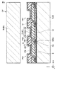
図1は、本発明の一態様に係る有機EL表示装置を概略的に示す平面図である。図2は、図1の表示装置に採用可能な構造の一例を概略的に示す断面図である。図3は、図2の表示装置が含む有機EL素子に採用可能な構造の一例を概略的に示す断面図である。図4は、図2の表示装置で採用可能な画素の配置の一例を概略的に示す平面図である。 FIG. 1 is a plan view schematically showing an organic EL display device according to an aspect of the present invention. FIG. 2 is a cross-sectional view schematically showing an example of a structure that can be employed in the display device of FIG. FIG. 3 is a cross-sectional view schematically showing an example of a structure that can be employed in the organic EL element included in the display device of FIG. FIG. 4 is a plan view schematically showing an example of pixel arrangement that can be employed in the display device of FIG.
図1及び図2の表示装置は、アクティブマトリクス型駆動方式を採用した上面発光型の有機EL表示装置である。この表示装置は、表示パネルDPと、映像信号線ドライバXDRと、走査信号線ドライバYDRとを含んでいる。 The display device of FIGS. 1 and 2 is a top emission type organic EL display device adopting an active matrix driving method. This display device includes a display panel DP, a video signal line driver XDR, and a scanning signal line driver YDR.
表示パネルDPは、例えば、ガラス基板などの絶縁基板SUBを含んでいる。基板SUB上には、図示しないアンダーコート層が形成されている。アンダーコート層は、例えば、基板SUB上にSiNx層とSiOx層とをこの順に積層してなる。 The display panel DP includes, for example, an insulating substrate SUB such as a glass substrate. An undercoat layer (not shown) is formed on the substrate SUB. The undercoat layer is formed, for example, by laminating a SiN x layer and a SiO x layer in this order on the substrate SUB.
アンダーコート層上には、例えば不純物を含有したポリシリコンからなる半導体パターンが形成されている。この半導体パターンの一部は、半導体層SCとして利用している。半導体層SCには、ソース及びドレインとして利用する不純物拡散領域が形成されている。また、この半導体パターンの他の一部は、後述するキャパシタCの下部電極として利用している。下部電極は、後述する画素PX1乃至PX3に対応して配列している。 On the undercoat layer, for example, a semiconductor pattern made of polysilicon containing impurities is formed. A part of this semiconductor pattern is used as the semiconductor layer SC. Impurity diffusion regions used as a source and a drain are formed in the semiconductor layer SC. Further, another part of the semiconductor pattern is used as a lower electrode of a capacitor C described later. The lower electrodes are arranged corresponding to pixels PX1 to PX3 described later.
なお、画素PX1乃至PX3は、この順にX方向に並んでおり、トリプレットを構成している。表示領域内では、このトリプレットがX方向とY方向とに配列されている。すなわち、表示領域内では、画素PX1をY方向に並べてなる画素列と、画素PX2をY方向に並べてなる画素列と、画素PX3をY方向に並べてなる画素列とがこの順にX方向に並べられ、さらに、これら3つの画素列がX方向に繰り返し並べられている。 Note that the pixels PX1 to PX3 are arranged in this order in the X direction to form a triplet. In the display area, the triplets are arranged in the X direction and the Y direction. That is, in the display area, a pixel column in which the pixels PX1 are arranged in the Y direction, a pixel column in which the pixels PX2 are arranged in the Y direction, and a pixel column in which the pixels PX3 are arranged in the Y direction are arranged in this order in the X direction. In addition, these three pixel columns are repeatedly arranged in the X direction.
半導体パターンは、ゲート絶縁膜GIによって被覆されている。ゲート絶縁膜GIは、例えばTEOS(tetraethyl orthosilicate)などを用いて形成することができる。ゲート絶縁膜GI上には、走査信号線SL1及びSL2が形成されている。走査信号線SL1及びSL2は、各々がX方向に延びており、Y方向に交互に配列している。走査信号線SL1及びSL2は、例えばMoWなどを用いて形成されている。 The semiconductor pattern is covered with the gate insulating film GI. The gate insulating film GI can be formed using, for example, TEOS (tetraethyl orthosilicate). Scan signal lines SL1 and SL2 are formed on the gate insulating film GI. The scanning signal lines SL1 and SL2 each extend in the X direction and are alternately arranged in the Y direction. The scanning signal lines SL1 and SL2 are formed using, for example, MoW.
ゲート絶縁膜GI上には、キャパシタCの上部電極がさらに配置されている。上部電極は、画素PX1乃至PX3に対応して配列しており、下部電極と向き合っている。上部電極は、例えばMoWなどを用いて形成され、走査信号線SL1及びSL2と同一の工程で形成することができる。 An upper electrode of the capacitor C is further disposed on the gate insulating film GI. The upper electrode is arranged corresponding to the pixels PX1 to PX3, and faces the lower electrode. The upper electrode is formed using, for example, MoW, and can be formed in the same process as the scanning signal lines SL1 and SL2.
走査信号線SL1及びSL2は、半導体層SCと交差している。走査信号線SL1と半導体層SCとの交差部は、スイッチングトランジスタSWaを構成している。走査信号線SL2と半導体層SCとの交差部は、スイッチングトランジスタSWb及びSWcを構成している。また、下部電極と上部電極とそれらの間に介在した絶縁膜GIとは、キャパシタCを構成している。上部電極は、半導体層SCと交差した延長部を含んでいる。延長部と半導体層SCとの交差部は、駆動トランジスタDRを構成している。 The scanning signal lines SL1 and SL2 intersect the semiconductor layer SC. The intersection of the scanning signal line SL1 and the semiconductor layer SC constitutes a switching transistor SWa. The intersection between the scanning signal line SL2 and the semiconductor layer SC constitutes switching transistors SWb and SWc. The lower electrode, the upper electrode, and the insulating film GI interposed therebetween constitute a capacitor C. The upper electrode includes an extension that intersects the semiconductor layer SC. A crossing portion between the extension portion and the semiconductor layer SC forms a drive transistor DR.
なお、この例では、駆動トランジスタDR及びスイッチングトランジスタSWa乃至SWcは、トップゲート型のpチャネル薄膜トランジスタである。また、図2において参照符号Gで示す部分は、スイッチングトランジスタSWaのゲートである。 In this example, the drive transistor DR and the switching transistors SWa to SWc are top-gate p-channel thin film transistors. In FIG. 2, the portion indicated by reference symbol G is the gate of the switching transistor SWa.
ゲート絶縁膜GI、走査信号線SL1及びSL2、並びに上部電極は、層間絶縁膜IIによって被覆されている。層間絶縁膜IIは、例えばプラズマCVD(chemical vapor deposition)法により堆積させたSiOxなどを用いて形成されている。 The gate insulating film GI, the scanning signal lines SL1 and SL2, and the upper electrode are covered with an interlayer insulating film II. The interlayer insulating film II is formed using, for example, SiO x deposited by a plasma CVD (chemical vapor deposition) method.
層間絶縁膜II上には、映像信号線DLと電源線PSLとが形成されている。映像信号線DLは、各々がY方向に延びており、X方向に配列している。電源線PSLは、例えば、各々がY方向に延びており、X方向に配列している。また、層間絶縁膜II上には、ソース電極SE及びドレイン電極DEが形成されている。ソース電極SE及びドレイン電極DEは、画素PX1乃至PX3の各々において素子同士を接続している。また、ソース電極SE及びドレイン電極DEは、層間絶縁膜IIに空けられたコンタクトホールにより、半導体層SCに設けられた不純物拡散領域に接続されている。 A video signal line DL and a power supply line PSL are formed on the interlayer insulating film II. Each of the video signal lines DL extends in the Y direction and is arranged in the X direction. For example, each of the power supply lines PSL extends in the Y direction and is arranged in the X direction. A source electrode SE and a drain electrode DE are formed on the interlayer insulating film II. The source electrode SE and the drain electrode DE connect elements in each of the pixels PX1 to PX3. The source electrode SE and the drain electrode DE are connected to an impurity diffusion region provided in the semiconductor layer SC by a contact hole opened in the interlayer insulating film II.
映像信号線DLと電源線PSLとソース電極SEとドレイン電極DEとは、例えば、Mo/Al/Moの三層構造を有している。これらは、同一工程で形成可能である。これらの映像信号線DLと電源線PSLとソース電極SEとドレイン電極DEとは、パッシベーション膜PSによって被覆されている。パッシベーション膜PSは、例えばSiNxなどを用いて形成されている。 The video signal line DL, the power supply line PSL, the source electrode SE, and the drain electrode DE have, for example, a three-layer structure of Mo / Al / Mo. These can be formed in the same process. The video signal line DL, the power supply line PSL, the source electrode SE, and the drain electrode DE are covered with a passivation film PS. The passivation film PS is formed using, for example, SiNx.
パッシベーション膜PS上では、画素電極(例えば第1電極に相当する)PEが、画素PX1乃至PX3に対応して配列している。各画素電極PEは、パッシベーション膜PSに設けたコンタクトホールを介してドレイン電極DEに接続されている。このドレイン電極は、スイッチングトランジスタSWaのドレインに接続されている。画素電極PEは、この例では陽極である。画素電極PEの材料としては、例えば、ITO(indium tin oxide)などの光透過性を有する導電材料を使用することができる。 On the passivation film PS, pixel electrodes (for example, corresponding to the first electrode) PE are arranged corresponding to the pixels PX1 to PX3. Each pixel electrode PE is connected to the drain electrode DE through a contact hole provided in the passivation film PS. This drain electrode is connected to the drain of the switching transistor SWa. The pixel electrode PE is an anode in this example. As a material of the pixel electrode PE, for example, a light-transmitting conductive material such as ITO (indium tin oxide) can be used.
パッシベーション膜PS上には、さらに、隔壁絶縁層PIが形成されている。隔壁絶縁層PIには、画素電極PEに対応した位置に貫通孔が設けられているか、或いは、画素電極PEが形成する列に対応した位置にスリットが設けられている。ここでは、一例として、隔壁絶縁層PIには、画素電極PEに対応した位置に貫通孔が設けられていることとする。隔壁絶縁層PIは、例えば、有機絶縁層である。隔壁絶縁層PIは、例えば、フォトリソグラフィ技術を用いて形成することができる。 A partition insulating layer PI is further formed on the passivation film PS. In the partition insulating layer PI, a through hole is provided at a position corresponding to the pixel electrode PE, or a slit is provided at a position corresponding to a column formed by the pixel electrode PE. Here, as an example, the partition insulating layer PI is provided with a through hole at a position corresponding to the pixel electrode PE. The partition insulating layer PI is, for example, an organic insulating layer. The partition insulating layer PI can be formed using, for example, a photolithography technique.
各画素電極PE上には、有機物層ORGが形成されている。有機物層ORGは、典型的には、図2に示すように、全ての画素PX1乃至PX3を含む表示領域に亘って広がった連続膜である。すなわち、有機物層ORGは、画素電極PEと隔壁絶縁層PIとを被覆している。 An organic layer ORG is formed on each pixel electrode PE. As shown in FIG. 2, the organic layer ORG is typically a continuous film extending over the display area including all the pixels PX1 to PX3. That is, the organic layer ORG covers the pixel electrode PE and the partition insulating layer PI.
隔壁絶縁層PI及び有機物層ORGは、対向電極(例えば第2電極に相当する)CEによって被覆されている。この例では、対向電極CEは、陰極であり、画素PX1乃至PX3で共用する共通電極である。対向電極CEは、例えば、パッシベーション膜PSと隔壁絶縁層PIとに設けられたコンタクトホールを介して、映像信号線DLと同一の層上に形成された電極配線(図示せず)に電気的に接続されている。 The partition insulating layer PI and the organic layer ORG are covered with a counter electrode (for example, corresponding to a second electrode) CE. In this example, the counter electrode CE is a cathode and a common electrode shared by the pixels PX1 to PX3. The counter electrode CE is electrically connected to an electrode wiring (not shown) formed on the same layer as the video signal line DL through, for example, a contact hole provided in the passivation film PS and the partition insulating layer PI. It is connected.
画素電極PEと有機物層ORGと対向電極CEとは、画素電極PEに対応して配列した有機EL素子OLEDを形成している。なお、図4において、参照符号EA1乃至EA3は、画素PX1乃至PX3が含む有機EL素子OLEDの発光部をそれぞれ示している。発光部EA1乃至EA3の各々は、Y方向に延びた直角四辺形である。図4の構造では、発光部EA1乃至EA3の面積は、互いに略等しい。 The pixel electrode PE, the organic layer ORG, and the counter electrode CE form an organic EL element OLED arranged in correspondence with the pixel electrode PE. In FIG. 4, reference numerals EA1 to EA3 indicate the light emitting portions of the organic EL elements OLED included in the pixels PX1 to PX3, respectively. Each of the light emitting units EA1 to EA3 is a right-angled quadrilateral extending in the Y direction. In the structure of FIG. 4, the areas of the light emitting portions EA1 to EA3 are substantially equal to each other.
画素PX1乃至PX3の各々は、図1に示すように、駆動トランジスタDRと、スイッチングトランジスタSWa乃至SWcと、有機EL素子OLEDと、キャパシタCとを含んでいる。上記の通り、この例では、駆動トランジスタDR及びスイッチングトランジスタSWa乃至SWcはpチャネル薄膜トランジスタである。 As shown in FIG. 1, each of the pixels PX1 to PX3 includes a drive transistor DR, switching transistors SWa to SWc, an organic EL element OLED, and a capacitor C. As described above, in this example, the drive transistor DR and the switching transistors SWa to SWc are p-channel thin film transistors.
駆動トランジスタDRとスイッチングトランジスタSWaと有機EL素子OLEDとは、第1電源端子ND1と第2電源端子ND2との間で、この順に直列に接続されている。この例では、電源端子ND1は高電位電源端子であり、電源端子ND2は低電位電源端子である。 The drive transistor DR, the switching transistor SWa, and the organic EL element OLED are connected in series in this order between the first power supply terminal ND1 and the second power supply terminal ND2. In this example, the power supply terminal ND1 is a high potential power supply terminal, and the power supply terminal ND2 is a low potential power supply terminal.
スイッチングトランジスタSWaのゲートは、走査信号線SL1に接続されている。スイッチングトランジスタSWbは映像信号線DLと駆動トランジスタDRのドレインとの間に接続されており、そのゲートは走査信号線SL2に接続されている。スイッチングトランジスタSWcは駆動トランジスタDRのドレインとゲートとの間に接続されており、そのゲートは走査信号線SL2に接続されている。キャパシタCは、駆動トランジスタDRのゲートと定電位端子ND1’との間に接続されている。この例では、定電位端子ND1’は、電源端子ND1に接続されている。 The gate of the switching transistor SWa is connected to the scanning signal line SL1. The switching transistor SWb is connected between the video signal line DL and the drain of the drive transistor DR, and its gate is connected to the scanning signal line SL2. The switching transistor SWc is connected between the drain and gate of the driving transistor DR, and the gate is connected to the scanning signal line SL2. The capacitor C is connected between the gate of the driving transistor DR and the constant potential terminal ND1 '. In this example, the constant potential terminal ND1 'is connected to the power supply terminal ND1.
映像信号線ドライバXDR及び走査信号線ドライバYDRは、基板SUB上に配置されている。すなわち、映像信号線ドライバXDR及び走査信号線ドライバYDRは、COG(chip on glass)実装されている。なお、映像信号線ドライバXDR及び走査信号線ドライバYDRは、COG実装する代わりに、TCP(tape carrier package)実装してもよい。或いは、映像信号線ドライバXDR及び走査信号線ドライバYDRは、基板SUB上に直接形成してもよい。 The video signal line driver XDR and the scanning signal line driver YDR are disposed on the substrate SUB. That is, the video signal line driver XDR and the scanning signal line driver YDR are mounted on a COG (chip on glass). Note that the video signal line driver XDR and the scanning signal line driver YDR may be mounted with TCP (tape carrier package) instead of being mounted with COG. Alternatively, the video signal line driver XDR and the scanning signal line driver YDR may be formed directly on the substrate SUB.
映像信号線ドライバXDRには、映像信号線DLが接続されている。この例では、映像信号線ドライバXDRには、電源線PSLがさらに接続されている。映像信号線ドライバXDRは、映像信号線DLに映像信号として電流信号を出力するとともに、電源線PSLに電源電圧を供給する。 A video signal line DL is connected to the video signal line driver XDR. In this example, a power supply line PSL is further connected to the video signal line driver XDR. The video signal line driver XDR outputs a current signal as a video signal to the video signal line DL and supplies a power supply voltage to the power supply line PSL.
走査信号線ドライバYDRには、走査信号線SL1及びSL2が接続されている。走査信号線ドライバYDRは、走査信号線SL1及びSL2にそれぞれ第1及び第2走査信号として電圧信号を出力する。 Scanning signal lines SL1 and SL2 are connected to the scanning signal line driver YDR. The scanning signal line driver YDR outputs voltage signals as first and second scanning signals to the scanning signal lines SL1 and SL2, respectively.
この有機EL表示装置で画像を表示する場合、例えば、走査信号線SL2を順次走査する。すなわち、画素PX1乃至PX3を行毎に選択する。或る行を選択している選択期間では、その行が含む画素PX1乃至PX3に対して書込動作を行なう。そして、その行を選択していない非選択期間では、その行が含む画素PX1乃至PX3で表示動作を行なう。 When an image is displayed on this organic EL display device, for example, the scanning signal line SL2 is sequentially scanned. That is, the pixels PX1 to PX3 are selected for each row. In a selection period in which a certain row is selected, a writing operation is performed on the pixels PX1 to PX3 included in the row. In the non-selection period in which the row is not selected, the display operation is performed on the pixels PX1 to PX3 included in the row.
或る行の画素PX1乃至PX3を選択する選択期間では、走査信号線ドライバYDRは、先の画素PX1乃至PX3が接続された走査信号線SL1にスイッチングトランジスタSWaを開く(非導通状態とする)走査信号を電圧信号として出力し、続いて、先の画素PX1乃至PX3が接続された走査信号線SL2にスイッチングトランジスタSWb及びSWcを閉じる(導通状態とする)走査信号を電圧信号として出力する。この状態で、映像信号線ドライバXDRは、映像信号線DLに映像信号を電流信号(書込電流)Isigとして出力し、駆動トランジスタDRのゲート−ソース間電圧Vgsを、先の映像信号Isigに対応した大きさに設定する。その後、走査信号線ドライバYDRは、先の画素PX1乃至PX3が接続された走査信号線SL2にスイッチングトランジスタSWb及びSWcを開く走査信号を電圧信号として出力し、続いて、先の画素PX1乃至PX3が接続された走査信号線SL1にスイッチングトランジスタSWaを閉じる走査信号を電圧信号として出力する。これにより、選択期間を終了する。 In the selection period in which the pixels PX1 to PX3 in a certain row are selected, the scanning signal line driver YDR performs scanning (opens a non-conducting state) to open the switching transistor SWa to the scanning signal line SL1 to which the previous pixels PX1 to PX3 are connected. The signal is output as a voltage signal, and subsequently, a scanning signal that closes the switching transistors SWb and SWc (sets the conductive state) to the scanning signal line SL2 to which the previous pixels PX1 to PX3 are connected is output as a voltage signal. In this state, the video signal line driver XDR outputs the video signal to the video signal line DL as a current signal (write current) I sig , and uses the gate-source voltage V gs of the drive transistor DR as the previous video signal I. A size corresponding to sig is set. Thereafter, the scanning signal line driver YDR outputs a scanning signal for opening the switching transistors SWb and SWc to the scanning signal line SL2 connected to the previous pixels PX1 to PX3 as a voltage signal, and then the previous pixels PX1 to PX3 A scanning signal for closing the switching transistor SWa is output as a voltage signal to the connected scanning signal line SL1. This ends the selection period.
選択期間に続く非選択期間では、スイッチングトランジスタSWaは閉じたままとし、スイッチングトランジスタSWb及びSWcは開いたままとする。非選択期間では、有機EL素子OLEDには、駆動トランジスタDRのゲート−ソース間電圧Vgsに対応した大きさの駆動電流Idrvが流れる。有機EL素子OLEDは、駆動電流Idrvの大きさに対応した輝度で発光する。ここで、Idrv≒Isigとなり、各画素で、電流信号(書込電流)Isigに対応した発光を得ることができる。 In the non-selection period following the selection period, the switching transistor SWa remains closed and the switching transistors SWb and SWc remain open. In the non-selection period, a drive current Idrv having a magnitude corresponding to the gate-source voltage Vgs of the drive transistor DR flows through the organic EL element OLED. The organic EL element OLED emits light with a luminance corresponding to the magnitude of the drive current Idrv . Here, I drv ≈I sig , and light emission corresponding to the current signal (write current) I sig can be obtained in each pixel.
尚、上記した例は、画素回路に映像信号として電流信号を書き込む構成を採用したものであるが、画素回路に映像信号として電圧信号を書き込む構成を採用することも可能であり、特に上記の例に限定したものではない。また、本態様では、pチャネル薄膜トランジスタを使用したが、nチャネル薄膜トランジスタを使用しても、本発明の本質を変えるものではない。 The above example employs a configuration in which a current signal is written as a video signal in the pixel circuit. However, a configuration in which a voltage signal is written in the pixel circuit as a video signal can also be employed. It is not limited to. In this embodiment, a p-channel thin film transistor is used. However, the use of an n-channel thin film transistor does not change the essence of the present invention.
また、有機EL素子OLEDの封止は、乾燥剤を付けたガラスなどによって形成した封止基板SUB2を表示領域の周辺に塗布したシール材で貼り合わせて実施する。 Further, the organic EL element OLED is sealed by bonding a sealing substrate SUB2 formed of glass with a desiccant or the like with a sealing material applied around the display area.
以下、本発明の実施例を説明する。
(実施例1)
本実施例では、3.0型WVGA有機ELディスプレイを作成した。画素サイズは82.5μm×27.5μmであり、画素数は800×3×480である。ここで、画素サイズは、画素PX1、画素PX2、画素PX3のそれぞれの大きさを示しており、本実施例では全て同じ大きさとした。また、本実施例では、画素電極PEのITOは厚さ50nmとした。
Examples of the present invention will be described below.
Example 1
In this example, a 3.0 type WVGA organic EL display was prepared. The pixel size is 82.5 μm × 27.5 μm, and the number of pixels is 800 × 3 × 480. Here, the pixel size indicates the size of each of the pixel PX1, the pixel PX2, and the pixel PX3. In the present embodiment, the pixel size is the same. In this embodiment, the ITO of the pixel electrode PE has a thickness of 50 nm.
本実施例では、図3に示すように、有機物層ORGは、赤色発光層EML1、緑色発光層EML2、及び、青色発光層EML3を積層して形成した。赤色発光層EML1、緑色発光層EML2、及び、青色発光層EML3は、それぞれ、全ての画素PX1乃至PX3を含む表示領域に亘って広がった連続膜として形成した。 In this example, as shown in FIG. 3, the organic layer ORG was formed by laminating a red light emitting layer EML1, a green light emitting layer EML2, and a blue light emitting layer EML3. The red light emitting layer EML1, the green light emitting layer EML2, and the blue light emitting layer EML3 were each formed as a continuous film extending over the display region including all the pixels PX1 to PX3.
ここで、赤色発光層EML1は、第1ホスト材料HM1と、発光色が赤色の第1ドーパント材料EM1との混合物によって形成されている。第1ドーパント材料EM1は、赤色波長に発光中心を有するルミネセンス性有機化合物又は組成物からなる赤色発光材料である。本実施例では、赤色発光層EML1としては、第1ホスト材料HM1:9,9-ビス(9-フェニル-9H-カルバゾル)フルオレン(略称;FL-2CBP)、及び、第1ドーパント材料EM1:4−(ジシアノメチレン)−2−メチル―6−(ジュロリジン―4−イル−ビニル)−4H−ピラン(略称;DCM2)からなる厚さ30nmの層を使用した。この赤色発光層EML1は、真空蒸着法により形成され、表示領域に亘って広がった連続膜とした。 Here, the red light emitting layer EML1 is formed of a mixture of the first host material HM1 and the first dopant material EM1 whose emission color is red. The first dopant material EM1 is a red light-emitting material made of a luminescent organic compound or composition having an emission center at a red wavelength. In this example, the red light emitting layer EML1 includes the first host material HM1: 9,9-bis (9-phenyl-9H-carbazol) fluorene (abbreviation: FL-2CBP), and the first dopant material EM1: 4. A 30 nm thick layer of-(dicyanomethylene) -2-methyl-6- (julolidin-4-yl-vinyl) -4H-pyran (abbreviation; DCM2) was used. The red light emitting layer EML1 was formed by a vacuum deposition method and was a continuous film extending over the display area.
第1ホスト材料HM1に要求される特性としては、その吸光度スペクトル特性において、第1ドーパント材料EM1の吸光度スペクトル特性における吸光度ピークよりも短波長側に吸光度ボトムを有していることである。 The characteristic required for the first host material HM1 is that the absorbance spectrum characteristic has an absorbance bottom on the shorter wavelength side than the absorbance peak in the absorbance spectrum characteristic of the first dopant material EM1.
緑色発光層EML2は、第2ホスト材料HM2と、発光色が緑色の第2ドーパント材料EM2との混合物によって形成されている。第2ドーパント材料EM2は、緑色波長に発光中心を有するルミネセンス性有機化合物又は組成物からなる緑色発光材料である。本実施例では、緑色発光層EML2としては、第2ホスト材料HM2:FL−2CBP、及び、第2ドーパント材料EM2:トリス(8−ヒドロキシキノラート)アルミニウム(略称;Alq3)からなる厚さ30nmの層を使用した。この緑色発光層EML2は、真空蒸着法により形成され、表示領域に亘って広がった連続膜とした。 The green light emitting layer EML2 is formed of a mixture of the second host material HM2 and the second dopant material EM2 having a green emission color. The second dopant material EM2 is a green light-emitting material made of a luminescent organic compound or composition having an emission center at a green wavelength. In this example, the green light emitting layer EML2 has a thickness of 30 nm made of the second host material HM2: FL-2CBP and the second dopant material EM2: tris (8-hydroxyquinolato) aluminum (abbreviation: Alq 3 ). Layers were used. The green light-emitting layer EML2 was formed by a vacuum deposition method and was a continuous film extending over the display area.
第2ホスト材料HM2に要求される特性としては、その吸光度スペクトル特性において、第1ドーパント材料EM1及び第2ドーパント材料EM2のそれぞれの吸光度スペクトル特性における吸光度ピークよりも短波長側に吸光度ボトムを有していることである。 As a characteristic required for the second host material HM2, the absorbance spectrum characteristic has an absorbance bottom on the shorter wavelength side than the absorbance peak in each of the absorbance spectrum characteristics of the first dopant material EM1 and the second dopant material EM2. It is that.
青色発光層EML3は、発光色が青色のルミネセンス性有機化合物又は組成物を含んだ薄膜である。この青色発光層EML3は、例えば、第3ホスト材料HM3と、発光色が青色の第3ドーパント材料EM3との混合物によって形成されている。本実施例では、青色発光層EML3としては、第3ホスト材料HM3:4,4’−ビス(2,2’−ジフェニル−エテン−1−イル)−ジフェニル(BPVBI)、及び、第3ドーパント材料EM3:ペリレンからなる厚さ30nmの層を使用した。この青色発光層EML3は、真空蒸着法により形成され、表示領域に亘って広がった連続膜とした。 The blue light-emitting layer EML3 is a thin film containing a luminescent organic compound or composition whose emission color is blue. The blue light emitting layer EML3 is formed of, for example, a mixture of the third host material HM3 and the third dopant material EM3 whose emission color is blue. In this example, as the blue light-emitting layer EML3, the third host material HM3: 4,4′-bis (2,2′-diphenyl-ethen-1-yl) -diphenyl (BPVBI), and the third dopant material A 30 nm thick layer of EM3: perylene was used. The blue light emitting layer EML3 was formed by a vacuum deposition method and was a continuous film extending over the display area.
なお、第1ホスト材料HM1及び第2ホスト材料HM2としては、上述した例の他に、1,3,5−トリス(カルバゾル−9−イル)ベンゼン(略称;TCP)を用いても良い。 As the first host material HM1 and the second host material HM2, 1,3,5-tris (carbazol-9-yl) benzene (abbreviation: TCP) may be used in addition to the above-described example.
本実施例では、上述したように、画素PX1、画素PX2、及び、画素PX3が同一構成の有機物層ORGを有していながら、画素PX1、画素PX2、及び、画素PX3の発光色は、互いに異なるように構成されている。ここに示した例では、画素PX1が含む有機EL素子OLEDは赤色に発光し、画素PX2が含む有機EL素子OLEDは緑色に発光し、画素PX3が含む有機EL素子OLEDは青色に発光する。 In the present embodiment, as described above, the pixel PX1, the pixel PX2, and the pixel PX3 have the organic layer ORG having the same configuration, but the emission colors of the pixel PX1, the pixel PX2, and the pixel PX3 are different from each other. It is configured as follows. In the example shown here, the organic EL element OLED included in the pixel PX1 emits red light, the organic EL element OLED included in the pixel PX2 emits green light, and the organic EL element OLED included in the pixel PX3 emits blue light.
なお、波長が400nm乃至435nmの範囲内にある光の色を紫、波長が435nm乃至480nmの範囲内にある光の色を青、波長が480nm乃至490nmの範囲内にある光の色を緑青、波長が490nm乃至500nmの範囲内にある光の色を青緑、波長が500nm乃至560nmの範囲内にある光の色を緑、波長が560nm乃至580nmの範囲内にある光の色を黄緑、波長が580nm乃至595nmの範囲内にある光の色を黄、波長が595nm乃至610nmの範囲内にある光の色を橙、波長が610nm乃至750nmの範囲内にある光の色を赤、波長が750nm乃至800nmの範囲内にある光の色を赤紫と定義するのが一般的であり、ここでは、主波長が400nm乃至490nmの範囲内にある光の色を青色、主波長が490nmより長く且つ595nmよりも短い光の色を緑色、主波長が595nm乃至800nmの範囲内にある光の色を赤色と定義する。 Note that the color of light having a wavelength in the range of 400 nm to 435 nm is purple, the color of light having a wavelength in the range of 435 nm to 480 nm is blue, the color of light having a wavelength in the range of 480 nm to 490 nm is patina, The color of light with a wavelength in the range of 490 nm to 500 nm is blue-green, the color of light with a wavelength in the range of 500 nm to 560 nm is green, the color of light with a wavelength in the range of 560 nm to 580 nm is yellow-green, The color of light having a wavelength in the range of 580 nm to 595 nm is yellow, the color of light having a wavelength in the range of 595 nm to 610 nm is orange, the color of light having a wavelength in the range of 610 nm to 750 nm is red, and the wavelength is Generally, the color of light in the range of 750 nm to 800 nm is defined as magenta. Here, the color of light having a dominant wavelength in the range of 400 nm to 490 nm is blue. Green color of light shorter than and dominant wavelength longer than 490 nm 595nm, the main wavelength is defined as the red color of the light in the range of 595nm to 800 nm.
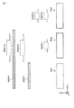
本実施例で適用した第1ドーパント材料EM1:DCM2、第2ドーパント材料EM2:Alq3、及び、第1ホスト材料HM1及び第2ホスト材料HM2であるFL-2CBPのそれぞれについて規格化した吸光度スペクトル特性を図5Aに示す。 Absorbance spectrum characteristics normalized for each of the first dopant material EM1: DCM2, the second dopant material EM2: Alq 3 , and the FL-2CBP that is the first host material HM1 and the second host material HM2 applied in this example. Is shown in FIG. 5A.
すなわち、第1ドーパント材料EM1であるDCM2は、図5Aにおいて(a)で示した吸光度スペクトル特性を有し、波長500nm付近に吸光度ピークを有している。また、第2ドーパント材料EM2であるAlq3は、図5Aにおいて(b)で示した吸光度スペクトル特性を有し、波長400nm付近に吸光度ピークを有している。 That is, DCM2, which is the first dopant material EM1, has the absorbance spectrum characteristic shown by (a) in FIG. 5A, and has an absorbance peak near the wavelength of 500 nm. Further, Alq 3 is a second dopant material EM2 has an absorbance spectrum characteristic shown in (b) in FIG. 5A, has an absorbance peak in the vicinity of a wavelength of 400 nm.
第1ホスト材料HM1及び第2ホスト材料HM2であるFL-2CBPは、図5Aにおいて(c)で示した吸光度スペクトル特性を有し、波長300nm付近に吸光度ピークを有している一方で、波長350nmから400nmの間に実質的な吸光度ボトムを有している。ここで、吸光度ボトムとは、規格化した吸光度スペクトル特性において、概略U字状に連続的に分布したスペクトルのうちの最底となる部分に相当し、また、概略L字状に連続的に分布したスペクトルのうちの底辺となり始める部分に相当し、規格化した吸光度が10%以下となっている。 FL-2CBP which is the first host material HM1 and the second host material HM2 has the absorbance spectrum characteristic shown in FIG. 5A by (c), and has an absorbance peak in the vicinity of a wavelength of 300 nm, while having a wavelength of 350 nm. From ˜400 nm with a substantial absorbance bottom. Here, the absorbance bottom corresponds to the bottom portion of the spectrum continuously distributed in a substantially U shape in the normalized absorbance spectrum characteristic, and continuously distributed in a substantially L shape. This corresponds to the part of the spectrum starting to become the bottom, and the normalized absorbance is 10% or less.
このFL−2CBPについては、波長350nmより短波長側においては、規格化吸光度が10%以上であるのに対して、波長360nm付近で吸光度ボトムとなり、それ以上の長波長においては概ね規格化吸光度が10%以下である。 For this FL-2CBP, the normalized absorbance is 10% or more on the shorter wavelength side than the wavelength of 350 nm, whereas the absorbance bottom is near the wavelength of 360 nm. 10% or less.
つまり、FL-2CBPの吸光度ボトムは、第1ドーパント材料EM1及び第2ドーパント材料EM2の吸光度ピークよりも短波長側にある。 That is, the absorbance bottom of FL-2CBP is on the shorter wavelength side than the absorbance peaks of the first dopant material EM1 and the second dopant material EM2.
また、本実施例において第1ホスト材料HM1及び第2ホスト材料HM2として適用可能なTCPについて、第1ドーパント材料EM1:DCM2、及び、第2ドーパント材料EM2:Alq3とともに、それぞれについて規格化した吸光度スペクトル特性を図5Bに示す。 Further, the applicable TCP as the first host material HM1 and second host material HM2 In this embodiment, the first dopant material EM1: DCM2, and, second dopant material EM2: with Alq 3, the absorbance was normalized for each The spectral characteristics are shown in FIG. 5B.
TCPは、図5Bにおいて(d)で示した吸光度スペクトル特性を有し、波長300nm付近に規格化吸光度のピークを有している一方で、波長350nmから400nmの間に実質的な吸光度ボトムを有している。このTCPについては、波長350nmより短波長側においては、規格化吸光度が10%以上であるのに対して、波長355nm付近で吸光度ボトムとなり、それ以上の長波長においては概ね規格化吸光度が10%以下である。 TCP has the absorbance spectrum characteristic indicated by (d) in FIG. 5B, and has a normalized absorbance peak near a wavelength of 300 nm, while having a substantial absorbance bottom between wavelengths of 350 nm and 400 nm. is doing. For this TCP, the normalized absorbance is 10% or more on the shorter wavelength side than the wavelength of 350 nm, whereas the absorbance bottom is near the wavelength of 355 nm, and the normalized absorbance is generally 10% at longer wavelengths. It is as follows.
つまり、TCPの吸光度ボトムは、第1ドーパント材料EM1及び第2ドーパント材料EM2の吸光度ピークよりも短波長側にある。 That is, the absorbance bottom of TCP is on the shorter wavelength side than the absorbance peaks of the first dopant material EM1 and the second dopant material EM2.
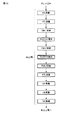
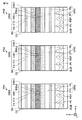
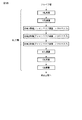
以下に製造方法を記載する。図6にそのプロセスフロー、図7に、図6中の露光工程の概略を示す。 The production method is described below. FIG. 6 shows the process flow, and FIG. 7 shows an outline of the exposure process in FIG.
まず、先に説明した表示パネルDPから対向電極CEと有機物層ORGを除いた構造,すなわちアレイ基板を、アレイ工程で準備する。 First, a structure obtained by removing the counter electrode CE and the organic layer ORG from the display panel DP described above, that is, an array substrate is prepared in an array process.
次に、画素電極PE上に、有機物層ORGが含む各層のうち、赤色発光層EML1を、真空蒸着法によって形成する。ここで、赤色発光層EML1は、表示領域に亘って広がった連続膜であり、画素毎に開口が形成されたファインマスクではなく、表示領域に対応した開口が形成されたラフマスクを使用したマスク蒸着で形成する。この工程を図6中に、EML1蒸着と示す。 Next, among the layers included in the organic layer ORG, the red light emitting layer EML1 is formed on the pixel electrode PE by a vacuum deposition method. Here, the red light emitting layer EML1 is a continuous film extending over the display area, and is not a fine mask in which an opening is formed for each pixel, but mask deposition using a rough mask in which an opening corresponding to the display area is formed. Form with. This process is shown as EML1 vapor deposition in FIG.
次に、画素PX2乃至PX3の領域に、波長が概略355〜800nmの光を、概略0.1mW・mm−2・nm−1(0.001〜1mW・mm−2・nm−1)の強度で照射する。このとき、画素PX1の領域には、フォトマスク(図7中のMASK1)を用いて、光が照射されないようにする。この工程を図6中に、PHOTO1露光と示す。 Next, light having a wavelength of approximately 355 to 800 nm is applied to the regions of the pixels PX2 to PX3 with an intensity of approximately 0.1 mW · mm −2 · nm −1 (0.001 to 1 mW · mm −2 · nm −1 ) Irradiate with. At this time, the region of the pixel PX1 is prevented from being irradiated with light by using a photomask (MASK1 in FIG. 7). This process is shown as PHOTO1 exposure in FIG.
次に、赤色発光層EML1上に、有機物層ORGが含む各層のうち、緑色発光層EML2を、ラフマスクを用いた真空蒸着法によって、表示領域に亘って広がった連続膜として形成する。この工程を図6中に、EML2蒸着と示す。 Next, on the red light emitting layer EML1, among the layers included in the organic layer ORG, the green light emitting layer EML2 is formed as a continuous film extending over the display region by a vacuum deposition method using a rough mask. This process is shown as EML2 vapor deposition in FIG.
次に、画素PX3の領域に、波長が概略355〜800nmの光を、概略0.1mW・mm−2・nm−1(0.001〜1mW・mm−2・nm−1)の強度で照射する。このとき、画素PX1乃至PX2には、フォトマスク(図7中のMASK2)を用いて、光が照射されないようにする。この工程を図6中に、PHOTO2露光と示す。 Next, light having a wavelength of approximately 355 to 800 nm is irradiated to the region of the pixel PX3 with an intensity of approximately 0.1 mW · mm −2 · nm −1 (0.001 to 1 mW · mm −2 · nm −1 ). To do. At this time, the pixels PX1 and PX2 are not irradiated with light by using a photomask (MASK2 in FIG. 7). This process is shown as PHOTO2 exposure in FIG.
次に、緑色発光層EML2上に、有機物層ORGが含む各層のうち、青色発光層EML3を、ラフマスクを用いた真空蒸着法によって、表示領域に亘って広がった連続膜として形成する。この工程を図6中に、EML3蒸着と示す。 Next, on the green light emitting layer EML2, among the layers included in the organic layer ORG, the blue light emitting layer EML3 is formed as a continuous film extending over the display region by a vacuum deposition method using a rough mask. This process is shown as EML3 vapor deposition in FIG.
その後、青色発光層EML3上に、対向電極CEを形成する。この工程を図6中にCE蒸着と示す。本実施例では、対向電極CEとしては、厚さ150nmのアルミニウム層を形成した。対向電極CEは、表示領域に亘って広がった連続膜とした。本実施例では、各発光層EMLでの発光をアレイ基板SUB側に取り出すための反射層も兼ねている。 Thereafter, the counter electrode CE is formed on the blue light emitting layer EML3. This process is shown as CE deposition in FIG. In this example, an aluminum layer having a thickness of 150 nm was formed as the counter electrode CE. The counter electrode CE was a continuous film extending over the display area. In this embodiment, it also serves as a reflective layer for taking out light emitted from each light emitting layer EML to the array substrate SUB side.
さらに、有機EL素子OLEDを封止し、表示パネルDPに映像信号線ドライバXDRと走査信号線ドライバYDRとを実装する。以上のようにして、図1及び図2の有機EL表示装置を得る。 Further, the organic EL element OLED is sealed, and the video signal line driver XDR and the scanning signal line driver YDR are mounted on the display panel DP. As described above, the organic EL display device of FIGS. 1 and 2 is obtained.
ここで、表示領域の開口に要求されるパターニング精度は、表示領域外に十分な寸法が取れるので、画素毎に塗り分けるパターニング精度よりも1桁以上低くても良い。したがって、ラフマスクに要求される開口精度は低く、金属製のマスクによるマスク蒸着でも十分に形成することができる。 Here, the patterning accuracy required for the opening of the display region can be sufficiently large outside the display region, and therefore may be lower by one digit or more than the patterning accuracy for coating each pixel. Therefore, the opening accuracy required for the rough mask is low, and it can be sufficiently formed even by mask vapor deposition using a metal mask.
一方、画素毎に光を照射する露光工程のパターニング精度は、フォトマスクを用いるので、照射する画素と照射しない画素とを高精度に分けることができる。すなわち、画素寸法の小さい場合でも、照射したい画素以外の領域に光を照射することがなく、処理することができる。 On the other hand, the patterning accuracy of the exposure process of irradiating light for each pixel uses a photomask, so that the pixels to be irradiated and the pixels not to be irradiated can be separated with high accuracy. That is, even when the pixel size is small, processing can be performed without irradiating light to a region other than the pixel to be irradiated.
ところで、1つの有機EL素子OLEDが複数の発光層EML1乃至EML3を含んでいると、1つの色だけでなく、他の色も発光する可能性がある。 By the way, when one organic EL element OLED includes a plurality of light emitting layers EML1 to EML3, there is a possibility that not only one color but also other colors emit light.
通常、発光層EML1乃至EML3を積層しただけの構成では、画素PX1乃至PX3は、全て同じ色に発光し、フルカラー表示を得ることができない。 Normally, in a configuration in which the light emitting layers EML1 to EML3 are simply stacked, the pixels PX1 to PX3 all emit light in the same color, and a full color display cannot be obtained.
そこで、本発明では、光を照射する画素と、光を照射しない画素とを、フォトマスクを用いた露光工程で分離し、各画素の発光色を制御する。 Therefore, in the present invention, pixels that irradiate light and pixels that do not irradiate light are separated by an exposure process using a photomask, and the emission color of each pixel is controlled.
図8は、本発明の画素の発光色を制御する原理の一つを示した図である。 FIG. 8 is a diagram showing one principle of controlling the emission color of the pixel of the present invention.
発光層EML1乃至EML3が積層された構造では、基本的には、赤色発光層EML1が発光しやすい。なぜなら、エネルギーの高い青色および緑色は、エネルギーの最も低い赤色発光層EML1に吸収され、赤色に変換されるので、このようなRGBの積層構造にした場合は、赤色が最も発光しやすい。したがって、光が照射されない画素PX1では、赤色が発光することになる。 In the structure in which the light emitting layers EML1 to EML3 are stacked, basically, the red light emitting layer EML1 easily emits light. This is because blue and green having high energy are absorbed by the red light emitting layer EML1 having the lowest energy and converted to red, and thus red is most likely to emit light in such an RGB laminated structure. Therefore, the pixel PX1 that is not irradiated with light emits red light.
次に、赤色発光層EML1の蒸着後の「PHOTO1露光」工程において、赤色発光層EML1に、波長が概略355〜800nmの光が照射された画素PX2では、第1ホスト材料HM1の吸光度ボトムより長い波長の光が照射されるため、第1ホスト材料HM1の吸光度が小さく、また、光を吸収しても第1ホスト材料HM1が、分解または重合または分子構造の変化が起きることはない。 Next, in the “PHOTO1 exposure” step after the deposition of the red light emitting layer EML1, in the pixel PX2 in which the red light emitting layer EML1 is irradiated with light having a wavelength of approximately 355 to 800 nm, it is longer than the absorbance bottom of the first host material HM1. Since the light having the wavelength is irradiated, the absorbance of the first host material HM1 is small, and even if the light is absorbed, the first host material HM1 does not decompose or undergo polymerization or change in the molecular structure.
それ故、355〜800nmの光を吸収した第1ドーパント材料EM1のみが、分解または重合または分子構造が変わることにより、赤色の光を発光しなくなる、所謂、消光する。つまり、画素PX2における発光層EML1乃至EML3のうち、赤色発光層EML1における第1ドーパント材料EM1が発光能を喪失している。この状態で、積層構造になると、赤色の次にエネルギーの低い緑色が発光しやすくなり、画素PX2は、緑色に発光するようになる。 Therefore, only the first dopant material EM1 that has absorbed light of 355 to 800 nm does not emit red light due to decomposition or polymerization or change in molecular structure, so-called quenching. That is, among the light emitting layers EML1 to EML3 in the pixel PX2, the first dopant material EM1 in the red light emitting layer EML1 loses light emitting ability. In this state, when a stacked structure is formed, green having the second lowest energy after red easily emits light, and the pixel PX2 emits green light.
更に、緑色発光層EML2の蒸着後「PHOTO2露光」工程において、緑色発光層EML2にも、波長が概略355〜800nmの光が照射された画素PX3では、第2ホスト材料HM2の吸光度ボトムより長い波長が照射されるため、第2ドーパント材料EM2のみが、光吸収により、分解または重合または分子構造が変わることにより、緑色の光を発光しなくなる。なお、この画素PX3については、「PHOTO1露光」工程において、赤色発光層EML1にも、波長が概略355〜800nmの光が照射されているため、第1ドーパント材料EM1が光吸収により、赤色の光を発光しなくなっている。
Further, in the “
つまり、画素PX3における発光層EML1乃至EML3のうち、赤色発光層EML1における第1ドーパント材料EM1及び緑色発光層EML2における第2ドーパント材料EM2が発光能を喪失している。この状態で、積層構造になると、青色よりエネルギーの低い発光をする層がなくなるので、青色が発光しやすくなり、画素PX3は、青色に発光するようになる。 That is, among the light-emitting layers EML1 to EML3 in the pixel PX3, the first dopant material EM1 in the red light-emitting layer EML1 and the second dopant material EM2 in the green light-emitting layer EML2 lose the light emitting ability. In this state, when a stacked structure is formed, since there is no layer that emits light lower in energy than blue, blue easily emits light, and the pixel PX3 emits blue light.
このとき、画素PX2では、赤色発光層EML1が、概略355〜800nmの光が照射で、第1ドーパント材料EM1を消光すると同時に、赤色発光層EML1のホール注入性またはホール輸送性が増し、光照射の無い場合、すなわち、画素PX1では、赤色発光層EML1にあった発光位置が、電子と正孔のバランスが変化することにより、緑色発光層EML2に移るようにする。これにより、画素PX2の発光効率が向上し、緑色の発光強度を増加させることができる。 At this time, in the pixel PX2, the red light emitting layer EML1 is irradiated with light of approximately 355 to 800 nm to quench the first dopant material EM1, and at the same time, the hole injecting property or hole transporting property of the red light emitting layer EML1 is increased. In other words, in the pixel PX1, the light emission position in the red light emitting layer EML1 is moved to the green light emitting layer EML2 by changing the balance of electrons and holes. Thereby, the light emission efficiency of the pixel PX2 can be improved, and the green light emission intensity can be increased.
また、同様に、画素PX3では、緑色発光層EML2が、概略355〜800nmの光が照射で、第2ドーパント材料EM2を消光すると同時に緑色発光層EML2のホール注入性またはホール輸送性が増し、画素PX2では、緑色発光層EML2にあった発光位置が、更に、電子と正孔のバランスが変化することにより、青色発光層EML3に移るようにする。これにより、画素PX3の発光効率が向上し、青色の発光強度を増加させることができる。 Similarly, in the pixel PX3, the green light emitting layer EML2 is irradiated with light of approximately 355 to 800 nm to quench the second dopant material EM2, and at the same time, the hole injecting property or hole transporting property of the green light emitting layer EML2 is increased. In PX2, the light emission position in the green light emitting layer EML2 is further moved to the blue light emitting layer EML3 by changing the balance of electrons and holes. Thereby, the light emission efficiency of the pixel PX3 can be improved, and the blue light emission intensity can be increased.
また、この例では、概略355〜800nmの光が照射で、赤色発光層EML1および緑色発光層EML2のホール注入性またはホール輸送性が増加する場合を記載したが、赤色発光層EML1および緑色発光層EML2の電子注入性または電子輸送性が低下することでも同様の効果を得ることができる。 Further, in this example, the case where the light injecting property or hole transporting property of the red light emitting layer EML1 and the green light emitting layer EML2 is increased by irradiation with light of approximately 355 to 800 nm is described, but the red light emitting layer EML1 and the green light emitting layer are described. The same effect can be obtained by reducing the electron injection property or electron transport property of EML2.
上述したように、赤色発光層EML1に含まれる第1ドーパント材料EM1、及び、緑色発光層EML2に含まれる第2ドーパント材料EM2を、露光により消光させる際、露光時間が短いほど、有機EL表示装置の生産性を向上することができる。 As described above, when the first dopant material EM1 included in the red light emitting layer EML1 and the second dopant material EM2 included in the green light emitting layer EML2 are quenched by exposure, the shorter the exposure time, the organic EL display device Productivity can be improved.
露光時間を短くする手段としては、露光強度を高くする方法がある。一般的な露光装置の光源である高圧水銀ランプの照射光波長は、200〜600nmの領域であり、その発光スペクトル特性において、発光強度が最大のピーク波長は365nmである。 As a means for shortening the exposure time, there is a method for increasing the exposure intensity. The irradiation light wavelength of a high-pressure mercury lamp, which is a light source of a general exposure apparatus, is in the range of 200 to 600 nm, and the peak wavelength with the maximum emission intensity is 365 nm in the emission spectrum characteristics.
この高圧水銀ランプの全ての波長を露光すると、照射強度が高くなるが、ドーパント材料だけでなく、ホスト材料も吸光する波長が含まれる。その際、ホスト材料が吸光したエネルギーの大部分は、エネルギーの低い赤色ドーパント材料に吸収されるが、ドーパント材料へ移行されなかったエネルギーによって、ホスト材料自身の分解または重合または分子構造の変化が起こる可能性がある。 When all the wavelengths of the high-pressure mercury lamp are exposed, the irradiation intensity increases, but not only the dopant material but also the wavelength at which the host material absorbs light is included. At that time, most of the energy absorbed by the host material is absorbed by the low-energy red dopant material, but the energy that is not transferred to the dopant material causes decomposition or polymerization of the host material itself or a change in molecular structure. there is a possibility.
ホスト材料は、EL発光時の電子やホールを輸送する機能や、ホスト材料自身が電子とホールのキャリア結合サイトとなり、フィルスター遷移によって励起エネルギーを、ドーパント材料に遷移する役割などがある。しかし、ホスト材料が、分解または重合または分子構造が変わることにより、このキャリア輸送性やキャリア結合サイトとしての性能が、低減する可能性があり、有機EL表示装置の性能が低減する問題が発生する。 The host material has a function of transporting electrons and holes at the time of EL light emission, and the host material itself serves as a carrier binding site between electrons and holes, and has a role of transferring excitation energy to a dopant material by a Filster transition. However, when the host material is decomposed or polymerized or the molecular structure is changed, there is a possibility that the carrier transportability and the performance as a carrier binding site may be reduced. .
そこで、ホスト材料がほとんど吸光することなく、赤色ドーパント材料または緑色ドーパント材料のみが吸光する波長を照射することが考えられる。しかしながら、このような場合には、波長を選択するための光学フィルターが適用されるため、露光の際には、照射波長を限定することによる照射強度の低減に加え、光学フィルター自身の吸収などにより光学フィルターを透過する際の照射強度の低減もあり、露光強度が低減し、露光時間が長くなるため、生産性が低減するおそれがある。 Therefore, it is conceivable that the host material irradiates a wavelength at which only the red dopant material or the green dopant material absorbs light with almost no light absorption. However, in such a case, since an optical filter for selecting the wavelength is applied, in the case of exposure, in addition to the reduction of irradiation intensity by limiting the irradiation wavelength, the optical filter itself absorbs, etc. There is also a reduction in the irradiation intensity when passing through the optical filter, the exposure intensity is reduced, and the exposure time is lengthened, which may reduce the productivity.
露光工程に用いる光の波長として、赤色発光層EML1に含まれる第1ホスト材料HM1及び緑色発光層EML2に含まれる第2ホスト材料HM2の吸光度スペクトル特性における吸光度ボトムよりも長波長の光を照射することにより、これらのホスト材料の分解または重合または分子構造の変化が起きない。 As a wavelength of light used in the exposure process, light having a wavelength longer than the absorbance bottom in the absorbance spectrum characteristics of the first host material HM1 included in the red light emitting layer EML1 and the second host material HM2 included in the green light emitting layer EML2 is irradiated. Therefore, decomposition or polymerization of these host materials or change in molecular structure does not occur.
一方で、発光能を消失させたい第1ドーパント材料EM1及び第2ドーパント材料EM2はその吸光度スペクトル特性においてホスト材料の吸光度ボトムよりも長波長側に吸光度ピークを有している。このため、露光工程においては、ホスト材料の吸光度ボトム付近の波長を含み、その波長から長波長の光を照射する。つまり、露光工程の露光波長は、紫外領域(200〜400nm)においてホスト材料の規格化吸光度が10%以下となる波長よりも長波長領域(光源のピーク波長を含む)と、可視光領域が全て使用できるため、露光強度を高く維持することができ、露光時間の短縮による生産性の向上を図ることが可能となる。 On the other hand, the first dopant material EM1 and the second dopant material EM2 for which the luminous ability is to be lost have an absorbance peak on the longer wavelength side than the absorbance bottom of the host material in the absorbance spectrum characteristics. For this reason, in the exposure process, light having a wavelength near the absorbance bottom of the host material is irradiated, and light having a long wavelength is irradiated from that wavelength. In other words, the exposure wavelength of the exposure process is all longer than the wavelength at which the normalized absorbance of the host material is 10% or less in the ultraviolet region (200 to 400 nm) (including the peak wavelength of the light source) and the visible light region. Since it can be used, the exposure intensity can be kept high, and the productivity can be improved by shortening the exposure time.
このように、本発明を適用することにより、画素毎にRGBを塗り分けるための金属製のファインマスクを使うことなく、RGB各画素に対応した色を発光させ、フルカラー表示を得ることできる。 As described above, by applying the present invention, it is possible to emit a color corresponding to each RGB pixel and obtain a full color display without using a metal fine mask for separately painting RGB for each pixel.
また、ファインマスクを使った蒸着の場合、マスク上に無駄な膜が形成されやすく、それにより、画素の開口の孔が塞いでしまう。それにより、画素に成膜される発光層EMLの成膜レートが低下し、より多くの材料を消費することになる。それに伴い、マスクを洗浄する回数が増える。これに対し、本発明では、開口が広く、マスク上に無駄な膜が形成され難いラフマスクのみを使うので、ファインマスクを使用した場合と比較して、より生産性が高く、環境負荷が少ない。 Further, in the case of vapor deposition using a fine mask, a useless film is likely to be formed on the mask, thereby blocking the opening of the pixel. As a result, the deposition rate of the light emitting layer EML deposited on the pixel is reduced, and more material is consumed. Accordingly, the number of times the mask is cleaned increases. On the other hand, in the present invention, only a rough mask that has a wide opening and is unlikely to form a useless film on the mask is used, so that the productivity is higher and the environmental load is less than when a fine mask is used.
したがって、本発明では、高精細、大形のフルカラー有機EL表示装置を、環境に優しく、高い生産性を持って提供することが可能になる。 Therefore, according to the present invention, it is possible to provide a high-definition, large-sized full-color organic EL display device that is environmentally friendly and has high productivity.
以上のようにして、図1および図2に示す本発明の有機EL表示装置を得た。 As described above, the organic EL display device of the present invention shown in FIGS. 1 and 2 was obtained.
その結果、画素PX1では、赤色が発光し、画素PX2では、緑色が発光し、画素PX3では、青色が、混色することなく発光した。それぞれ、発光効率は、赤色が、8cd/A、(0.65,0.35)、緑色が10cd/A、(0.30,0.60)、青色が3cd/A、(0.14,0.12)であった。 As a result, the pixel PX1 emitted red light, the pixel PX2 emitted green light, and the pixel PX3 emitted blue light without being mixed. The luminous efficiencies of red are 8 cd / A, (0.65, 0.35), green is 10 cd / A, (0.30, 0.60), blue is 3 cd / A, (0.14, respectively). 0.12).
なお、上述の値は、画面を正面から観察したときに100cd/m2の輝度で(x,y)=(0.31,0.315)の基準白色(C)が表示されるようにし、画素PX1乃至PX3を順次点灯し、発光色毎に輝度と色度(x,y)とを測定した値である。 The above-mentioned value is such that when the screen is observed from the front, the reference white (C) of (x, y) = (0.31, 0.315) is displayed with a luminance of 100 cd / m 2 . This is a value obtained by sequentially lighting the pixels PX1 to PX3 and measuring the luminance and chromaticity (x, y) for each emission color.
また、本実施例では、画素PX1、画素PX2、画素PX3を全て同じ大きさとしたが、例えば、各画素の発光色の輝度劣化寿命を揃えるために、画素の大きさは、異ならせても良い。これにより、白色が着色しにくくすることができる。 In the present embodiment, the pixels PX1, PX2, and PX3 are all the same size. However, for example, the pixels may be different in size in order to make the luminance degradation life of the emission colors of the respective pixels uniform. . Thereby, white can be made difficult to color.
(比較例1:従来例)
図24は、比較例1(従来例)に係る有機EL表示装置が含む有機EL素子の構造を概略的に示す断面図である。また、図25にそのプロセスフローを示す。
(Comparative example 1: Conventional example)
FIG. 24 is a cross-sectional view schematically showing the structure of the organic EL element included in the organic EL display device according to Comparative Example 1 (conventional example). FIG. 25 shows the process flow.
本例では、発光層EML1乃至EML3に図24の構造を採用したこと以外は実施例1について説明したのと同様の方法により、図1及び図2の有機EL表示装置を製造した。 In this example, the organic EL display device of FIGS. 1 and 2 was manufactured by the same method as described in Example 1 except that the structure of FIG. 24 was adopted for the light emitting layers EML1 to EML3.
具体的には、本例では、赤色発光層EML1は、正孔輸送層HTL上であって、画素PX1の画素電極PEに対応した位置に形成した。赤色発光層EML1は、画素PX1の列に対応して開口が設けられたファインマスクを用いた真空蒸着法により形成した。赤色発光層EML1の位置は、基板SUB上の目標位置に正確に一致させた。赤色発光層EML1の厚さは30nmとした。 Specifically, in this example, the red light emitting layer EML1 is formed on the hole transport layer HTL and at a position corresponding to the pixel electrode PE of the pixel PX1. The red light emitting layer EML1 was formed by a vacuum deposition method using a fine mask provided with openings corresponding to the columns of the pixels PX1. The position of the red light emitting layer EML1 was exactly matched to the target position on the substrate SUB. The thickness of the red light emitting layer EML1 was 30 nm.
緑色発光層EML2は、正孔輸送層HTL上であって、画素PX2の画素電極PEに対応した位置に形成した。緑色発光層EML2は、画素PX2の列に対応して開口が設けられたファインマスクを用いた真空蒸着法により形成した。緑色発光層EML2の位置は、基板SUB上の目標位置に正確に一致させた。緑色発光層EML2の厚さは30nmとした。 The green light emitting layer EML2 was formed on the hole transport layer HTL at a position corresponding to the pixel electrode PE of the pixel PX2. The green light emitting layer EML2 was formed by a vacuum evaporation method using a fine mask provided with openings corresponding to the columns of the pixels PX2. The position of the green light emitting layer EML2 was exactly matched to the target position on the substrate SUB. The thickness of the green light emitting layer EML2 was 30 nm.
青色発光層EML3は、正孔輸送層HTL上であって、画素PX3の画素電極PEに対応した位置に形成した。青色発光層EML3は、画素PX3の列に対応して開口が設けられたファインマスクを用いた真空蒸着法により形成した。青色発光層EML3の位置は、基板SUB上の目標位置に正確に一致させた。青色発光層EML3の厚さは30nmとした。 The blue light emitting layer EML3 was formed on the hole transport layer HTL at a position corresponding to the pixel electrode PE of the pixel PX3. The blue light-emitting layer EML3 was formed by a vacuum deposition method using a fine mask provided with openings corresponding to the columns of the pixels PX3. The position of the blue light emitting layer EML3 was exactly matched to the target position on the substrate SUB. The thickness of the blue light emitting layer EML3 was 30 nm.
この例では、金属製のファインマスクにより、画素PX1(赤)、画素PX2(緑)、画素PX3(青)に、正確に各発光層EMLをパターニングする必要があるが、この金属製のマスクは、蒸着源の熱により撓みやすく、特に画素の小さい高精細のパネルでは、正確な位置にパターニングし難く、発光層EMLの位置ずれが多発する。発光層EMLの位置ずれは、例えば、赤色の画素に緑色または青色の発光層EMLがはみ出し、赤色に緑色または青色の発光色が混じる。所謂、混色不良が発生する。 In this example, it is necessary to accurately pattern each light emitting layer EML on the pixel PX1 (red), the pixel PX2 (green), and the pixel PX3 (blue) with a metal fine mask. In the case of a high-definition panel that is easily bent by the heat of the vapor deposition source and that has a small pixel size, it is difficult to perform patterning at an accurate position, and misalignment of the light emitting layer EML occurs frequently. As for the positional deviation of the light emitting layer EML, for example, the green or blue light emitting layer EML protrudes from the red pixel, and the green or blue light emitting color is mixed with red. A so-called color mixing failure occurs.
また、従来例では、金属性のファインマスクが画素の発光層EMLに直接接触し、発光層EMLを傷つけてしまうのを防ぐために、マスクを支持するための隔壁絶縁層も必要になる。これが無い場合は、画素電極PEと対向電極がショートし、滅点不良が多発する。この隔壁絶縁層は、1μm以上の膜厚が必要である。 Further, in the conventional example, in order to prevent the metallic fine mask from being in direct contact with the light emitting layer EML of the pixel and damaging the light emitting layer EML, a partition insulating layer for supporting the mask is also required. When this is not present, the pixel electrode PE and the counter electrode are short-circuited, resulting in frequent dark spot defects. This partition insulating layer needs to have a thickness of 1 μm or more.
以下、本発明の別の実施例を示す。 Hereinafter, another embodiment of the present invention will be described.
(実施例2:露光工程の順番を変える場合)
この例の構造は、図3の構造と同様である。図9にそのプロセスフローを示す。
(Example 2: When changing the order of exposure steps)
The structure of this example is the same as the structure of FIG. FIG. 9 shows the process flow.
この例では、PHOTO1露光及びPHOTO2露光をEML3蒸着後に連続して行なう。また、PHOTO1露光及びPHOTO2露光では、照射する光の主波長を変える。 In this example, PHOTO1 exposure and PHOTO2 exposure are continuously performed after EML3 deposition. In the PHOTO1 exposure and the PHOTO2 exposure, the main wavelength of the irradiated light is changed.
すなわち、PHOTO1露光では、画素PX2及びPX3に対して、赤色発光層EML1の第1ドーパント材料EM1のみが吸収する波長を主波長とした光を照射する。これにより、第1ドーパント材料EM1が分解または重合または分子構造が変わることにより、光を照射された領域の赤色発光層EML1が赤色に発光する発光能を喪失する。そして、本発明のように発光層EML1乃至EML3が積層構造になっている場合には、赤色の次にエネルギーの低い緑色が発光しやすくなり、画素PX2は、緑色に発光するようになる。 That is, in the PHOTO1 exposure, the pixels PX2 and PX3 are irradiated with light whose main wavelength is a wavelength absorbed only by the first dopant material EM1 of the red light emitting layer EML1. Accordingly, the first dopant material EM1 is decomposed or polymerized, or the molecular structure is changed, so that the red light emitting layer EML1 in the region irradiated with light loses the light emitting ability to emit red light. When the light emitting layers EML1 to EML3 have a laminated structure as in the present invention, green having the second lowest energy after red easily emits light, and the pixel PX2 emits green light.
PHOTO2露光では、画素PX3に対して、緑色発光層EML2の第2ドーパント材料EM2のみが吸収する波長を主波長とした光を照射する。これにより、第2ドーパント材料EM2が分解または重合または分子構造が変わることにより、光を照射された領域のEML2が緑色に発光する発光能を喪失する。そして、本発明のように発光層EML1乃至EML3が積層構造になっている場合には、一番エネルギーの高い青色が発光しやすくなり、画素PX3は、青色に発光するようになる。 In the PHOTO2 exposure, the pixel PX3 is irradiated with light whose main wavelength is a wavelength that is absorbed only by the second dopant material EM2 of the green light emitting layer EML2. As a result, the second dopant material EM2 is decomposed or polymerized or the molecular structure is changed, so that the light emission ability of the EML2 in the region irradiated with light to emit green light is lost. When the light emitting layers EML1 to EML3 have a laminated structure as in the present invention, blue having the highest energy is easily emitted, and the pixel PX3 emits blue light.
このように、露光工程を発光層EML1乃至EML3の蒸着後に連続して行なうことにより、真空蒸着装置に基板を出し入れすることを少なくでき、真空状態を達成するまでの待機時間も少なくなり、生産性が向上する。 Thus, by performing the exposure process continuously after the deposition of the light-emitting layers EML1 to EML3, it is possible to reduce the number of substrates that are taken in and out of the vacuum deposition apparatus, and the waiting time until the vacuum state is achieved is reduced. Will improve.
(実施例3:発光層EML以外に、HIL、HTL、ETL、EILを付加した場合)
図10に、この例の構造を示す。図10は、図2の表示装置が含む有機EL素子OLEDに採用可能な構造の他の一例を概略的に示す断面図である。また、図11にそのプロセスフローを示す。
(Example 3: When HIL, HTL, ETL, EIL is added in addition to the light emitting layer EML)
FIG. 10 shows the structure of this example. FIG. 10 is a cross-sectional view schematically showing another example of a structure that can be employed in the organic EL element OLED included in the display device of FIG. FIG. 11 shows the process flow.
この例では、有機物層ORGは、発光層EML1乃至EML3の積層体に加えて、ホール注入層HIL、ホール輸送層HTL、電子輸送層ETL、及び、電子注入層EILを有している。 In this example, the organic layer ORG includes a hole injection layer HIL, a hole transport layer HTL, an electron transport layer ETL, and an electron injection layer EIL in addition to the stacked body of the light emitting layers EML1 to EML3.
正孔注入層HILとしては、厚さ10nmのアモルファスカーボン層を形成した。この正孔注入層HILは、表示領域に亘って広がった連続膜とした。 As the hole injection layer HIL, an amorphous carbon layer having a thickness of 10 nm was formed. The hole injection layer HIL was a continuous film extending over the display region.
正孔輸送層HTLとしては、N,N’−ジフェニル−N,N’−ビス(1−ナフチルフェニル)−1,1’−ビフェニル−4,4’−ジアミン(α−NPD)からなる厚さ30nmの層を真空蒸着法により形成した。この正孔輸送層HTLは、表示領域に亘って広がった連続膜とした。 The hole transport layer HTL has a thickness composed of N, N′-diphenyl-N, N′-bis (1-naphthylphenyl) -1,1′-biphenyl-4,4′-diamine (α-NPD). A 30 nm layer was formed by vacuum evaporation. The hole transport layer HTL was a continuous film extending over the display region.
電子輸送層ETLとしては、厚さ30nmのAlq3層を使用した。この電子輸送層ETLは、真空蒸着法により形成し、表示領域に亘って広がった連続膜とした。 As the electron transport layer ETL, an Alq 3 layer having a thickness of 30 nm was used. The electron transport layer ETL was formed by a vacuum vapor deposition method and was a continuous film extending over the display region.
電子注入層EILとしては、厚さ1nmの弗化リチウム層を使用した。この電子注入層EILは、表示領域に亘って広がった連続膜とした。 As the electron injection layer EIL, a lithium fluoride layer having a thickness of 1 nm was used. The electron injection layer EIL was a continuous film extending over the display area.
これにより、発光層内でのホール、電子のバランスが改善され、発光効率が良くなる。また、ホール注入、ホール輸送、電子注入および電子輸送が良好になり、駆動電圧が低減する。 Thereby, the balance of holes and electrons in the light emitting layer is improved, and the light emission efficiency is improved. In addition, hole injection, hole transport, electron injection and electron transport are improved, and the driving voltage is reduced.
(実施例4:上面発光の場合)
図12にこの例の構造を示す。図12は、図2の表示装置が含む有機EL素子OLEDに採用可能な構造の他の一例を概略的に示す断面図である。
(Example 4: Case of top emission)
FIG. 12 shows the structure of this example. FIG. 12 is a cross-sectional view schematically showing another example of a structure that can be employed in the organic EL element OLED included in the display device of FIG.
この例では、各有機EL素子OLEDは、画素電極PEの有機物層ORGにおける積層体(EML1乃至EML3)と対向する側とは反対側、つまり、画素電極PEと基板SUBとの間に反射層REFを備えている。これにより、対向電極CE側に発光が取り出される。対向電極CEは、半透明電極とし、マグネシウムと銀の混合蒸着で作成した。対向電極CEの厚さは、20nmとし、表示領域に亘って広がった連続膜とした。また、マグネシウムと銀との比率は、高光透過性を有するためには、銀を60〜98%含有する構成とした。 In this example, each organic EL element OLED has a reflective layer REF that is opposite to the side of the organic layer ORG of the pixel electrode PE that faces the stacked body (EML1 to EML3), that is, between the pixel electrode PE and the substrate SUB. It has. Thereby, light emission is extracted to the counter electrode CE side. The counter electrode CE was a semi-transparent electrode and was prepared by mixed vapor deposition of magnesium and silver. The thickness of the counter electrode CE was 20 nm, and a continuous film spread over the display area. Further, the ratio of magnesium to silver is set to contain 60 to 98% of silver in order to have high light transmittance.
これにより、基板SUB側に発光を取り出す構造と異なり、薄膜トランジスタやその配線による開口率の制限を受けることなく、光を取り出すことができる。 Thus, unlike the structure in which light emission is extracted to the substrate SUB side, light can be extracted without being limited by the aperture ratio due to the thin film transistor and its wiring.
したがって、画素の小さい高精細のパネルでも有機EL素子OLEDの発光面積が十分に取れるようになり、有機EL素子OLEDの通電劣化(寿命)が改善する。 Therefore, even in a high-definition panel with small pixels, the light emitting area of the organic EL element OLED can be sufficiently taken, and the energization deterioration (life) of the organic EL element OLED is improved.
(実施例5:上面発光で露光工程を、対向電極形成後に実施する場合)
図13に本実施例のプロセスフローを示す。この例では、対向電極CEを形成するための蒸着工程後に、露光工程PHOTO1およびPHOTO2を実施する。本実施例のプロセスは、対向電極CEに透過性が必要なため、図12の有機EL素子OLEDの構造のような、EL発光を対向電極CE側に取り出す構造が必要になる。
(Example 5: When the exposure process is performed after the formation of the counter electrode with top emission)
FIG. 13 shows a process flow of this embodiment. In this example, after the vapor deposition process for forming the counter electrode CE, the exposure processes PHOTO1 and PHOTO2 are performed. In the process of this embodiment, since the counter electrode CE needs to have transparency, a structure for extracting EL light emission to the counter electrode CE side, such as the structure of the organic EL element OLED in FIG.
本実施例では、対向電極CEまでの真空工程の途中に露光工程を追加しないため、工程間での真空引きなどのロスを減らすことができ、露光工程のトータルタクトタイムを減らすことができる。また、それに伴いより有機EL素子OLEDを形成するため製造装置の負荷を減らすことができる。 In this embodiment, since an exposure process is not added in the middle of the vacuum process up to the counter electrode CE, loss such as evacuation between processes can be reduced, and the total tact time of the exposure process can be reduced. In addition, the load on the manufacturing apparatus can be reduced because the organic EL element OLED is formed.
(実施例6:上面発光構造にHIL、HTL、ETL、EILおよび光学マッチング層MCを付加した場合)
図14にこの例の構造を示す。図14は、図2の表示装置が含む有機EL素子OLEDに採用可能な構造の他の一例を概略的に示す断面図である。また、図15には、そのプロセスフローを示す。図14の構造は、図12の構造に、ホール注入層HIL、ホール輸送層HTL、電子輸送層ETL、電子注入層EILを付加し、さらに、対向電極CEの上(つまり、有機物層ORGにおける積層体と対向する側とは反対側)に光学マッチング層MCを形成した。
(Example 6: When HIL, HTL, ETL, EIL, and optical matching layer MC are added to the top light emitting structure)
FIG. 14 shows the structure of this example. FIG. 14 is a cross-sectional view schematically showing another example of a structure that can be employed in the organic EL element OLED included in the display device of FIG. FIG. 15 shows the process flow. In the structure of FIG. 14, a hole injection layer HIL, a hole transport layer HTL, an electron transport layer ETL, and an electron injection layer EIL are added to the structure of FIG. The optical matching layer MC was formed on the side opposite to the side facing the body.
光学マッチング層MCは、光透過性の層であって、絶縁基板SUBと封止基板SUB2との間隙にある窒素などの気体層との光学的なマッチングを図る。光学マッチング層MCの屈折率は、有機物層ORGの屈折率とほぼ等しい。例えば、光学マッチング層MCとしては、SiON層などの透明無機絶縁層、ITO層などの透明無機導電層、有機物層ORGが含んでいる層などの透明有機物層を使用することができる。光学マッチング層MCを使用すると、光取り出し効率を高めることができる。 The optical matching layer MC is a light-transmitting layer, and optically matches a gas layer such as nitrogen in the gap between the insulating substrate SUB and the sealing substrate SUB2. The refractive index of the optical matching layer MC is substantially equal to the refractive index of the organic layer ORG. For example, as the optical matching layer MC, a transparent inorganic insulating layer such as a SiON layer, a transparent inorganic conductive layer such as an ITO layer, or a transparent organic layer such as a layer included in the organic layer ORG can be used. When the optical matching layer MC is used, the light extraction efficiency can be increased.
本実施例では、画素電極PEの膜厚を100nm、ホール輸送層HTLを75nmとした。光学マッチング層MCは70nmとした。 In this embodiment, the pixel electrode PE has a thickness of 100 nm and the hole transport layer HTL has a thickness of 75 nm. The optical matching layer MC was 70 nm.
これにより、実施例4と比較して、発光効率を4倍向上することができ、実施例4と同じ白輝度設定とした場合、消費電力を1/4にすることができた。 As a result, the luminous efficiency can be improved by a factor of 4 compared to Example 4, and the power consumption can be reduced to 1/4 when the white luminance setting is the same as that of Example 4.
(実施例7:上面発光構造にHIL、HTL、ETL、EILおよび光学マッチング層MCおよびRGB干渉条件調整層MC2を付加した場合)
図16にこの例の構造を示す。図16は、図2の表示装置が含む有機EL素子OLEDに採用可能な構造の他の一例を概略的に示す断面図である。図16の構造は、図14の構造に、RGB各画素PX1、PX2およびPX3の干渉条件を調整する干渉条件調整層MC2を対向電極CEと反射層REFとの間(ここでは、画素電極PEと反射層REFとの間)に形成した。
(Example 7: When HIL, HTL, ETL, EIL, optical matching layer MC, and RGB interference condition adjusting layer MC2 are added to the top light emitting structure)
FIG. 16 shows the structure of this example. FIG. 16 is a cross-sectional view schematically showing another example of a structure that can be employed in the organic EL element OLED included in the display device of FIG. The structure of FIG. 16 is different from the structure of FIG. 14 in that an interference condition adjustment layer MC2 for adjusting the interference condition of each of the RGB pixels PX1, PX2, and PX3 is provided between the counter electrode CE and the reflective layer REF (here, the pixel electrode PE and (Between the reflective layer REF).
干渉条件調整層MC2は、光透過性の層であって、この例のような上面発光構造の場合の反射層REFと対向電極CEとの間の光路長を発光色の波長に合せて最適化設計する必要がある。特に、赤色Rと緑色Gと青色Bでは、同じ干渉次数では、その発光波長の違いから、最適な光路長(共振条件)が異なるが、それら3色の発光波長の1/4の最小公倍数に相当する光路長になるような干渉条件調整層MC2を反射層REFと対向電極CEの間に形成することにより、画素PX1乃至PX3の発光色、赤、緑、青の発光が効率よく取り出され、発光効率が向上し、より低消費電力化が図れる。 The interference condition adjustment layer MC2 is a light-transmitting layer, and the optical path length between the reflective layer REF and the counter electrode CE in the case of the top emission structure as in this example is optimized according to the wavelength of the emission color. Need to design. In particular, red R, green G, and blue B have different optical wavelengths (resonance conditions) due to differences in their emission wavelengths at the same interference order, but the least common multiple of 1/4 of the emission wavelengths of these three colors. By forming the interference condition adjustment layer MC2 having a corresponding optical path length between the reflective layer REF and the counter electrode CE, the emission colors of the pixels PX1 to PX3, red, green, and blue emission are efficiently extracted, Luminous efficiency is improved and lower power consumption can be achieved.
干渉調整層MC2の屈折率は、有機物層ORGの屈折率とほぼ等しい。干渉条件調整層MC2は、例えば、SiN層などの透明無機絶縁層、ITO層などの透明無機導電層、有機物層ORGが含んでいる層などの透明有機物層を使用することができる。 The refractive index of the interference adjustment layer MC2 is substantially equal to the refractive index of the organic layer ORG. As the interference condition adjusting layer MC2, for example, a transparent inorganic insulating layer such as a SiN layer, a transparent inorganic conductive layer such as an ITO layer, and a transparent organic layer such as a layer included in the organic layer ORG can be used.
本実施例では、ホール輸送層HTLの膜厚を40nmとし、干渉条件調整層MC2には、SiNを使用し、膜厚を410nmとした。 In this example, the thickness of the hole transport layer HTL was 40 nm, SiN was used for the interference condition adjustment layer MC2, and the thickness was 410 nm.
これにより、実施例4と比較して、発光効率を6倍、実施例6と比較して、1.5倍にすることができ、消費電力を低減することができた。また、本実施例では、赤、緑、青の各色の色純度が向上し、色再現性範囲を100%以上(対NTSC比)にすることができた。 As a result, the luminous efficiency was 6 times that of Example 4 and 1.5 times that of Example 6, and the power consumption was reduced. Further, in this example, the color purity of each color of red, green, and blue was improved, and the color reproducibility range could be 100% or more (vs. NTSC ratio).
(実施例8:上面発光構造の干渉条件調整層MC2を青画素PX3だけ抜き)
図17にこの例の構造を示す。図17は、図2の表示装置が含む有機EL素子OLEDに採用可能な構造の他の一例を概略的に示す断面図である。図17の構造は、図16の構造で画素PX3(青色)の干渉条件調整層MC2を抜く構造とした。
(Example 8: Only the blue pixel PX3 is removed from the interference condition adjustment layer MC2 having a top emission structure)
FIG. 17 shows the structure of this example. FIG. 17 is a cross-sectional view schematically showing another example of a structure that can be employed in the organic EL element OLED included in the display device of FIG. The structure of FIG. 17 is a structure in which the interference condition adjustment layer MC2 of the pixel PX3 (blue) is removed from the structure of FIG.
これにより、干渉条件(共振条件)を,各色の画素で合せやすくなり、効率をより向上でき、各色の色純度も向上することができる。 As a result, the interference condition (resonance condition) can be easily adjusted for each color pixel, the efficiency can be further improved, and the color purity of each color can also be improved.
本実施例では、干渉条件調整層MC2の膜厚を、赤色と緑色のみに合せ、390nmとした。これにより、発光効率が向上し、実施例7と比較して、発光効率を更に1.5倍にすることができ、消費電力を低減することができた。 In this example, the thickness of the interference condition adjusting layer MC2 was set to 390 nm only for red and green. Thereby, the luminous efficiency was improved, and the luminous efficiency could be further increased by 1.5 times compared to Example 7, and the power consumption could be reduced.
(実施例9:上面発光構造に凹凸散乱層を作成する)
図18にこの例の構造を示す。図18は、図2の表示装置が含む有機EL素子OLEDに採用可能な構造の他の一例を概略的に示す断面図である。図18の構造は、図14の構造に上面発光の共振状態をなくす散乱層を含む凹凸散乱層を、画素電極PEと基板SUBとの間(つまり、画素電極PEの有機物層ORGにおける積層体と対向する側とは反対側)に形成した。この凹凸散乱層は、反射層REFと有機材料を用いて形成した。
(Example 9: Create an uneven scattering layer on the top light emitting structure)
FIG. 18 shows the structure of this example. 18 is a cross-sectional view schematically showing another example of a structure that can be employed in the organic EL element OLED included in the display device of FIG. In the structure of FIG. 18, the uneven scattering layer including the scattering layer that eliminates the resonance state of the top emission from the structure of FIG. 14 is formed between the pixel electrode PE and the substrate SUB (that is, It was formed on the side opposite to the opposite side. The uneven scattering layer was formed using the reflective layer REF and an organic material.
これにより、干渉条件(共振条件)が無くなり、各有機EL素子OLEDの膜厚調整が必要なくなる。 Thereby, the interference condition (resonance condition) is eliminated, and the film thickness adjustment of each organic EL element OLED becomes unnecessary.
(実施例10:上面発光構造の画素PX1(赤)および画素PX2(緑)に凹凸散乱層を作成する)
図19にこの例の構造を示す。図19は、図2の表示装置が含む有機EL素子OLEDに採用可能な構造の他の一例を概略的に示す断面図である。図19の構造は、図14の構造の画素PX1(赤色)、画素PX2(緑色)に上面発光の共振状態をなくす凹凸散乱層構造を反射層REFと有機材料を用いて形成した。
(Example 10: An uneven scattering layer is formed on the pixel PX1 (red) and the pixel PX2 (green) having a top emission structure)
FIG. 19 shows the structure of this example. FIG. 19 is a cross-sectional view schematically showing another example of a structure that can be employed in the organic EL element OLED included in the display device of FIG. In the structure of FIG. 19, the uneven scattering layer structure that eliminates the resonance state of the top emission is formed on the pixel PX1 (red) and the pixel PX2 (green) of the structure of FIG. 14 using the reflective layer REF and an organic material.
これにより、干渉条件(共振条件)は、画素PX3(青色)に合せてのみ設計すればよく、特に効率が低く、電力を消費する青色の効率をより向上でき、青色の色純度も向上することができる。 Accordingly, the interference condition (resonance condition) only needs to be designed according to the pixel PX3 (blue), and the efficiency is particularly low, the efficiency of blue that consumes power can be further improved, and the color purity of blue is also improved. Can do.
(実施例11:HTL蒸着後に露光PHOTO3を追加する)
図20に、この例のプロセスフローを示す。この例では、ホール輸送層HTLを形成する蒸着工程の後に、露光PHOTO3を実施することで、ホール輸送層HTLがその後の露光プロセスで電気特性が変化しないようにする。
(Example 11: Exposure PHOTO3 is added after HTL deposition)
FIG. 20 shows a process flow of this example. In this example, the exposure PHOTO3 is performed after the vapor deposition step for forming the hole transport layer HTL so that the electrical characteristics of the hole transport layer HTL are not changed in the subsequent exposure process.
これにより、画素の発光を制御する露光プロセスPHOTO1およびPHOTO2の露光条件の自由度を増すことができ、より発光色の制御がしやすくなる。 As a result, the degree of freedom of the exposure conditions PHOTO1 and PHOTO2 for controlling the light emission of the pixels can be increased, and the emission color can be controlled more easily.
(実施例12:ETL蒸着後に露光PHOTO4を追加する)
図21にこの例のプロセスフローを示す。この例では、電子輸送層ETLを形成する蒸着工程の後に、露光PHOTO4を実施することで、所望の画素(画素PX2または画素PX3または画素PX2およびPX3の両方)の電子輸送層ETLの電子移動度または電子注入度を変化させる。
(Example 12: Exposure PHOTO4 is added after ETL deposition)
FIG. 21 shows a process flow of this example. In this example, exposure PHOTO4 is performed after the vapor deposition step for forming the electron transport layer ETL, so that the electron mobility of the electron transport layer ETL of the desired pixel (pixel PX2 or pixel PX3 or both pixels PX2 and PX3) is obtained. Alternatively, the degree of electron injection is changed.
これにより、所望の画素のキャリアバランスを向上させ、発光効率を向上させることができる。 Thereby, the carrier balance of a desired pixel can be improved and the light emission efficiency can be improved.
(実施例13:ETL蒸着後に露光PHOTO5,6を追加する)
図22にこの例のプロセスフローを示す。この例では、電子輸送層ETLを形成する蒸着工程の後に、露光PHOTO5および露光PHOTO6を実施することで、画素PX1、画素PX2、画素PX3それぞれの有機物層ORGの電気的特性を変化させ、キャリアバランスをそれぞれの画素(発光色)に最適になるように変化させる。
(Example 13: Exposure PHOTO5 and 6 are added after ETL deposition)
FIG. 22 shows a process flow of this example. In this example, the exposure PHOTO5 and the exposure PHOTO6 are performed after the vapor deposition process for forming the electron transport layer ETL, thereby changing the electrical characteristics of the organic layer ORG of each of the pixels PX1, PX2, and PX3, and carrier balance. Are changed to be optimal for each pixel (light emission color).
なお、露光PHOTO5および露光PHOTO6では、照射する光の主波長を変えてもよい。 In the exposure PHOTO5 and the exposure PHOTO6, the main wavelength of the irradiated light may be changed.
これにより、画素PX1、PX2、PX3のそれぞれのキャリアバランスが向上し、それぞれの発光効率を向上させることができる。 Thereby, the carrier balance of each of the pixels PX1, PX2, and PX3 is improved, and the respective light emission efficiency can be improved.
(実施例14:隔壁絶縁層PI(リブ)を使用しない場合)
本実施例では、有機EL素子OLEDを用いた表示装置に通常用いる画素間に形成する隔壁絶縁層PIを形成しない構成とした。これは、本発明では、金属製のマスクを使用しないため、真空蒸着の際にそれを支持するための隔壁絶縁層が不要なためである。
(Example 14: When the partition insulating layer PI (rib) is not used)
In this embodiment, the partition insulating layer PI formed between pixels normally used in a display device using the organic EL element OLED is not formed. This is because a metal mask is not used in the present invention, and therefore a partition insulating layer for supporting it during vacuum deposition is unnecessary.
これにより、隔壁絶縁層PIを形成する工程を削減でき、使用材料を削減でき、環境負荷を更に減らすことができる。 Thereby, the process of forming the partition insulating layer PI can be reduced, the material used can be reduced, and the environmental load can be further reduced.
(実施例15:ハーフトーン露光を使用する場合)
図23にこの例のプロセスフローを示す。本実施例では,実施例1と比較して、第2有機EL素子OLEDに、第3有機EL素子の露光強度より小さい強度の露光を、ハーフトーンマスクを利用して、1回の露光(ハーフトーン露光)工程で実施した。
(Example 15: When halftone exposure is used)
FIG. 23 shows a process flow of this example. In the present embodiment, compared to the first embodiment, the second organic EL element OLED is exposed to light having an intensity smaller than the exposure intensity of the third organic EL element by using a halftone mask for one exposure (half half). (Tone exposure) step.
これにより、露光工程が簡略化され、生産性が向上する。 This simplifies the exposure process and improves productivity.
(実施例16:露光時の装置内酸素濃度を20ppm以上にする場合)
図6、図9、図11、図13、図15、図20、図21、図22のPHOTO1露光とPHOTO2露光において、露光装置内の酸素濃度が1ppm以下の条件と、20ppmの条件とでは、酸素濃度20ppm環境下の方が、赤色もしくは、緑色発光(ドーパント)材料が消光しやすい。
(Example 16: When the oxygen concentration in the apparatus at the time of exposure is set to 20 ppm or more)
6, 9, 11, 13, 15, 20, 21, and 22, in the HOTO1 exposure and PHOTO2 exposure, the oxygen concentration in the exposure apparatus is 1 ppm or less and the condition is 20 ppm The red or green light emitting (dopant) material is more easily quenched when the oxygen concentration is 20 ppm.
例えば、ホスト材料:FL−2CBP、第2ドーパント材料:トリ(2−フィニルピリジン) イリジウム(III)(略称;Ir(ppy)3)からなる、ドーパント濃度8%、厚さ30nm膜を、ガラス基板の上に真空蒸着法により形成する。そして、この作成した膜に、酸素濃度が1ppm以下環境下と、20ppm環境下との双方にて、水銀キセノンランプ光源を用いて、355nm以上の光を10分間照射し、照射前後のPLスペクトルを比較すると、光照射前の緑色発光材料:Ir(ppy)3のPL強度を100%とした場合、酸素濃度1ppm以下の環境では49%まで低減するのに対して、酸素濃度20ppm環境では38%まで低減した。 For example, a host material: FL-2CBP, a second dopant material: tri (2-finylpyridine) iridium (III) (abbreviation: Ir (ppy) 3), a dopant concentration of 8% and a thickness of 30 nm is formed from glass. It is formed on the substrate by vacuum deposition. Then, this prepared film was irradiated with light of 355 nm or more for 10 minutes using a mercury xenon lamp light source in both an oxygen concentration environment of 1 ppm or less and a 20 ppm environment, and PL spectra before and after irradiation were obtained. In comparison, when the PL intensity of the green light emitting material: Ir (ppy) 3 before light irradiation is 100%, it is reduced to 49% in an environment with an oxygen concentration of 1 ppm or less, whereas it is 38% in an environment with an oxygen concentration of 20 ppm. Reduced to.
先述の通り、355nm以上の光照射では、ホスト材料:FL−2CBPは分解等の変化は起きないので、光照射によるPL強度の低減は、緑色発光(ドーパント)材料:Ir(ppy)3の消光によるものである。 As described above, since the host material: FL-2CBP does not undergo degradation or other changes when irradiated with light of 355 nm or more, the PL intensity is reduced by the irradiation of light. The green emission (dopant) material: Ir (ppy) 3 is quenched. Is due to.
それ故、発光(ドーパント)材料を消光する、図6、図9、図11、図13、図15、図20、図21、図22のPHOTO1露光及びPHOTO2露光において、酸素濃度が20ppm以上の環境下で露光した方が、露光時間を短縮できるため、生産性が向上する。 Therefore, the environment in which the oxygen concentration is 20 ppm or more in the PHOTO1 exposure and the PHOTO2 exposure of FIGS. 6, 9, 11, 13, 15, 15, 20, 21, and 22 that quench the luminescent (dopant) material. When exposed below, the exposure time can be shortened, so productivity is improved.
なお、上記の実施例では、有機EL表示装置は、発光色が異なる3種の有機EL素子を含んでいる。有機EL表示装置は、有機EL素子として、発光色が異なる2種の有機EL素子のみを含んでいてもよく、発光色が異なる4種以上の有機EL素子を含んでいてもよい。 In the above embodiment, the organic EL display device includes three types of organic EL elements having different emission colors. The organic EL display device may include only two types of organic EL elements with different emission colors as the organic EL element, or may include four or more types of organic EL elements with different emission colors.
C…キャパシタ、CE…対向電極、DE…ドレイン電極、DL…映像信号線、DP…表示パネル、DR…駆動トランジスタ、EA1…発光部、EA2…発光部、EA3…発光部、EIL…電子注入層、EML…発光層、EML1…赤色発光層、EML2…緑色発光層、EML3…青色発光層、EM1…第1ドーパント材料(赤色発光材料)、EM2…第2ドーパント材料(緑色発光材料)、EM3…第3ドーパント材料(青色発光材料)、ETL…電子輸送層、G…ゲート、GI…ゲート絶縁膜、HIL…正孔注入層、HM1…第1ホスト材料、HM2…第2ホスト材料、HM3…第3ホスト材料、HTL…正孔輸送層、II…層間絶縁膜、MC…マッチング層、ND1…電源端子、ND1’…定電位端子、ND2…電源端子、OLED…有機EL素子、ORG…有機物層、PE…画素電極、PI…隔壁絶縁層、PS…パッシベーション膜、PSL…電源線、PX1…画素(赤色画素)、PX2…画素(緑色画素)、PX3…画素(青色画素)、REF…反射層、SC…半導体層、SE…ソース電極、SL1…走査信号線、SL2…走査信号線、SUB…絶縁基板、SUB2…封止基板、SWa…スイッチングトランジスタ、SWb…スイッチングトランジスタ、SWc…スイッチングトランジスタ、XDR…映像信号線ドライバ、YDR…走査信号線ドライバ、干渉条件調整層…MC2。 C ... capacitor, CE ... counter electrode, DE ... drain electrode, DL ... video signal line, DP ... display panel, DR ... drive transistor, EA1 ... light emitting part, EA2 ... light emitting part, EA3 ... light emitting part, EIL ... electron injection layer , EML ... light emitting layer, EML1 ... red light emitting layer, EML2 ... green light emitting layer, EML3 ... blue light emitting layer, EM1 ... first dopant material (red light emitting material), EM2 ... second dopant material (green light emitting material), EM3 ... Third dopant material (blue light emitting material), ETL ... electron transport layer, G ... gate, GI ... gate insulating film, HIL ... hole injection layer, HM1 ... first host material, HM2 ... second host material, HM3 ... first 3 Host material, HTL ... Hole transport layer, II ... Interlayer insulating film, MC ... Matching layer, ND1 ... Power supply terminal, ND1 '... Constant potential terminal, ND2 ... Power supply terminal, OLED ... Yes EL element, ORG ... organic layer, PE ... pixel electrode, PI ... partition insulating layer, PS ... passivation film, PSL ... power line, PX1 ... pixel (red pixel), PX2 ... pixel (green pixel), PX3 ... pixel (blue) Pixel), REF ... reflective layer, SC ... semiconductor layer, SE ... source electrode, SL1 ... scanning signal line, SL2 ... scanning signal line, SUB ... insulating substrate, SUB2 ... sealing substrate, SWa ... switching transistor, SWb ... switching transistor , SWc, switching transistor, XDR, video signal line driver, YDR, scanning signal line driver, interference condition adjustment layer, MC2.
Claims (6)
前記第1絶縁膜の上に配置された第1電極と、
前記第1絶縁膜の上に配置された第2電極と、
前記第1電極と前記第2電極との間に配置された第2絶縁膜と、
第1ドーパント材料と、前記第1ドーパント材料の吸光度スペクトル特性における吸光度ピークよりも短波長側に吸光度ボトムを有する第1ホスト材料と、を有し、前記第1電極、前記第2電極、及び、前記第2絶縁膜の上方に配置された第1発光層と、
前記第1ドーパント材料とは異なる第2ドーパント材料と、前記第1ドーパント材料及び前記第2ドーパント材料の吸光度スペクトル特性における吸光度ピークよりも短波長側に吸光度ボトムを有する第2ホスト材料と、を有し、前記第1電極、前記第2電極、及び、前記第2絶縁膜の上方であって且つ前記第1発光層の上に配置された第2発光層と、
前記第1電極、前記第2電極、及び、前記第2絶縁膜の上方であって且つ前記第2発光層の上方に配置された第3電極と、を具備し、
前記第2電極の上方の前記第1発光層が有する前記第1ドーパント材料、及び、前記第2電極の上方の前記第2発光層が有する前記第2ドーパント材料の内、吸光度ピークの波長が長い方のドーパント材料は、消光していることを特徴とする有機EL装置。 A first insulating film;
A first electrode disposed on the first insulating film;
A second electrode disposed on the first insulating film,
A second insulating film disposed between the first electrode and the second electrode;
And a first host material having an absorbance bottom on a shorter wavelength side than an absorbance peak in an absorbance spectrum characteristic of the first dopant material, the first electrode, the second electrode, and A first light emitting layer disposed above the second insulating film;
A second dopant material different from the first dopant material, and a second host material having an absorbance bottom on a shorter wavelength side than an absorbance peak in absorbance spectrum characteristics of the first dopant material and the second dopant material. A second light-emitting layer disposed on the first light-emitting layer and above the first electrode, the second electrode, and the second insulating film;
The first electrode, the second electrode, and a third electrode disposed above the second insulating film and above the second light emitting layer , and
Of the first dopant material of the first light emitting layer above the second electrode and the second dopant material of the second light emitting layer above the second electrode, the wavelength of the absorbance peak is long. The organic dopant is characterized in that the dopant material is quenched .
前記第1絶縁膜の上に配置された第1電極と、
前記第1絶縁膜の上に配置された第2電極と、
前記第1絶縁膜の上に配置された第3電極と、
前記第1電極と前記第2電極との間、及び、前記第2電極と前記第3電極との間にそれぞれ配置された第2絶縁膜と、
第1ドーパント材料と、前記第1ドーパント材料の吸光度スペクトル特性における吸光度ピークよりも短波長側に吸光度ボトムを有する第1ホスト材料と、を有し、前記第1電極、前記第2電極、前記第3電極、及び、前記第2絶縁膜の上方に配置された第1発光層と、
前記第1ドーパント材料とは異なる第2ドーパント材料と、前記第1ドーパント材料及び前記第2ドーパント材料の吸光度スペクトル特性における吸光度ピークよりも短波長側に吸光度ボトムを有する第2ホスト材料と、を有し、前記第1電極、前記第2電極、前記第3電極、及び、前記第2絶縁膜の上方であって且つ前記第1発光層の上に配置された第2発光層と、
前記第1ドーパント材料及び前記第2ドーパント材料とは異なる第3ドーパント材料と、第3ホスト材料と、を有し、前記第1電極、前記第2電極、前記第3電極、及び、前記第2絶縁膜の上方であって且つ前記第2発光層の上に配置された第3発光層と、
前記第1電極、前記第2電極、前記第3電極、及び、前記第2絶縁膜の上方であって且つ前記第3発光層の上方に配置された第4電極と、を具備し、
前記第2電極の上方の前記第1発光層が有する前記第1ドーパント材料、前記第3電極の上方の前記第1発光層が有する前記第1ドーパント材料、及び、前記第3電極の上方の前記第2発光層が有する前記第2ドーパント材料は、消光していることを特徴とする有機EL装置。 A first insulating film;
A first electrode disposed on the first insulating film;
A second electrode disposed on the first insulating film,
A third electrode disposed on the first insulating film,
A second insulating film disposed between the first electrode and the second electrode and between the second electrode and the third electrode;
A first host material having an absorbance bottom on a shorter wavelength side than an absorbance peak in an absorbance spectrum characteristic of the first dopant material, the first electrode, the second electrode, the first Three electrodes, and a first light emitting layer disposed above the second insulating film;
A second dopant material different from the first dopant material, and a second host material having an absorbance bottom on a shorter wavelength side than an absorbance peak in absorbance spectrum characteristics of the first dopant material and the second dopant material. A second light emitting layer disposed above the first light emitting layer and above the first electrode, the second electrode, the third electrode, and the second insulating film;
A third dopant material different from the first dopant material and the second dopant material, and a third host material, the first electrode, the second electrode, the third electrode, and the second A third light emitting layer disposed above the insulating film and on the second light emitting layer;
The first electrode, the second electrode, the third electrode, and a fourth electrode disposed above the second insulating film and above the third light emitting layer ,
The first dopant material included in the first light emitting layer above the second electrode, the first dopant material included in the first light emitting layer above the third electrode, and the above the third electrode. The organic EL device , wherein the second dopant material included in the second light emitting layer is quenched .
前記第1絶縁膜の上に第1電極、第2電極、及び、第3電極を形成し、
前記第1電極と前記第2電極との間、及び、前記第2電極と前記第3電極との間にそれぞれ第2絶縁膜を形成し、
第1ドーパント材料と、前記第1ドーパント材料の吸光度スペクトル特性における吸光度ピークよりも短波長側に吸光度ボトムを有する第1ホスト材料と、を用いて、前記第1電極、前記第2電極、前記第3電極、及び、前記第2絶縁膜の上方に第1発光層を形成し、
前記第1ドーパント材料とは異なる第2ドーパント材料と、前記第1ドーパント材料及び前記第2ドーパント材料の吸光度スペクトル特性における吸光度ピークよりも短波長側に吸光度ボトムを有する第2ホスト材料と、を用いて、前記第1電極、前記第2電極、前記第3電極、及び、前記第2絶縁膜の上方であって且つ前記第1発光層の上に第2発光層を形成し、
前記第1ドーパント材料及び前記第2ドーパント材料とは異なる第3ドーパント材料と、第3ホスト材料と、を用いて、前記第1電極、前記第2電極、前記第3電極、及び、前記第2絶縁膜の上方であって且つ前記第2発光層の上に第3発光層を形成し、
前記第1電極、前記第2電極、前記第3電極、及び、前記第2絶縁膜の上方であって且つ前記第3発光層の上方に第4電極を形成し、
前記第2電極の上方の前記第1ドーパント材料、前記第3電極の上方の前記第1ドーパント材料、及び、前記第3電極の上方の前記第2ドーパント材料を露光して消光する、
ことを特徴とする有機EL装置の製造方法。 Forming a first insulating film;
First electrode, a second electrode on the first insulating film, and forming a third electrode,
Forming a second insulating film between the first electrode and the second electrode and between the second electrode and the third electrode;
Using the first dopant material and the first host material having an absorbance bottom on the shorter wavelength side than the absorbance peak in the absorbance spectrum characteristic of the first dopant material, the first electrode, the second electrode, the first Forming a first light emitting layer above the three electrodes and the second insulating film;
A second dopant material different from the first dopant material, and a second host material having an absorbance bottom on a shorter wavelength side than an absorbance peak in absorbance spectrum characteristics of the first dopant material and the second dopant material are used. Forming a second light-emitting layer on the first light-emitting layer above the first electrode, the second electrode, the third electrode, and the second insulating film;
Using a third dopant material different from the first dopant material and the second dopant material, and a third host material, the first electrode, the second electrode, the third electrode, and the second Forming a third light emitting layer above the insulating film and on the second light emitting layer;
Forming a fourth electrode above the first light emitting layer, above the first electrode, the second electrode, the third electrode, and the second insulating film ;
Exposing and quenching the first dopant material above the second electrode, the first dopant material above the third electrode, and the second dopant material above the third electrode;
A method for manufacturing an organic EL device.
Priority Applications (4)
| Application Number | Priority Date | Filing Date | Title |
|---|---|---|---|
| JP2008093438A JP4745362B2 (en) | 2008-03-31 | 2008-03-31 | Organic EL device and manufacturing method thereof |
| TW98108956A TWI470787B (en) | 2008-03-31 | 2009-03-19 | Organic el display device and method of manufacturing the same |
| US12/408,993 US7915813B2 (en) | 2008-03-31 | 2009-03-23 | Organic EL display device and method of manufacturing the same |
| US12/977,781 US8283854B2 (en) | 2008-03-31 | 2010-12-23 | Organic EL display device and method of manufacturing the same |
Applications Claiming Priority (1)
| Application Number | Priority Date | Filing Date | Title |
|---|---|---|---|
| JP2008093438A JP4745362B2 (en) | 2008-03-31 | 2008-03-31 | Organic EL device and manufacturing method thereof |
Publications (3)
| Publication Number | Publication Date |
|---|---|
| JP2009245870A JP2009245870A (en) | 2009-10-22 |
| JP2009245870A5 JP2009245870A5 (en) | 2009-12-24 |
| JP4745362B2 true JP4745362B2 (en) | 2011-08-10 |
Family
ID=41307516
Family Applications (1)
| Application Number | Title | Priority Date | Filing Date |
|---|---|---|---|
| JP2008093438A Active JP4745362B2 (en) | 2008-03-31 | 2008-03-31 | Organic EL device and manufacturing method thereof |
Country Status (1)
| Country | Link |
|---|---|
| JP (1) | JP4745362B2 (en) |
Families Citing this family (5)
| Publication number | Priority date | Publication date | Assignee | Title |
|---|---|---|---|---|
| JP2011113736A (en) * | 2009-11-25 | 2011-06-09 | Toshiba Mobile Display Co Ltd | Organic el device, and method of manufacturing the same |
| JP2011191739A (en) | 2010-02-16 | 2011-09-29 | Toshiba Mobile Display Co Ltd | Organic electroluminescence device |
| JP6207263B2 (en) * | 2013-07-03 | 2017-10-04 | 株式会社ジャパンディスプレイ | Organic EL display device and manufacturing method thereof |
| JP6963163B2 (en) * | 2018-01-19 | 2021-11-05 | 株式会社クオルテック | EL display panel manufacturing method and EL display device |
| WO2020136849A1 (en) * | 2018-12-27 | 2020-07-02 | シャープ株式会社 | Display device, and method for manufacturing display device |
Family Cites Families (2)
| Publication number | Priority date | Publication date | Assignee | Title |
|---|---|---|---|---|
| TW542851B (en) * | 1996-05-15 | 2003-07-21 | Chemipro Kasei Kaisha Ltd | Multicolor organic electroluminescence element, its manufacturing method, and a display using the same |
| JP4797438B2 (en) * | 2005-05-17 | 2011-10-19 | ソニー株式会社 | Organic electroluminescence device and display device |
-
2008
- 2008-03-31 JP JP2008093438A patent/JP4745362B2/en active Active
Also Published As
| Publication number | Publication date |
|---|---|
| JP2009245870A (en) | 2009-10-22 |
Similar Documents
| Publication | Publication Date | Title |
|---|---|---|
| JP4775863B2 (en) | Organic EL display device and manufacturing method thereof | |
| KR100961343B1 (en) | Organic el display and method of manufacturing the same | |
| JP2009111023A (en) | Organic el display device and manufacturing method thereof | |
| JP5127265B2 (en) | Organic EL display device | |
| JP5019638B2 (en) | Organic EL display device | |
| US8283854B2 (en) | Organic EL display device and method of manufacturing the same | |
| JP5094477B2 (en) | Organic light-emitting display device and method for manufacturing the same | |
| US20120018749A1 (en) | Organic light emitting display apparatus and method for manufacturing the same | |
| KR20180066948A (en) | Organic light-emitting display apparatus | |
| JP2007005173A (en) | Display device | |
| JP2006041471A (en) | Organic electroluminescent device and its manufacturing method | |
| JP2009016298A (en) | Organic light-emitting display device and its manufacturing method | |
| US9150954B2 (en) | Light-emitting diode and deposition apparatus for fabricating the same | |
| JP5305267B2 (en) | Organic EL device | |
| JP3481231B2 (en) | Organic electroluminescent display device and method of manufacturing the same | |
| JP4745362B2 (en) | Organic EL device and manufacturing method thereof | |
| JP4544645B2 (en) | Manufacturing method of organic EL display device | |
| KR20080042008A (en) | Organic el element and organic el display | |
| KR101069036B1 (en) | Organic el display device and method of manufacturing the same |
Legal Events
| Date | Code | Title | Description |
|---|---|---|---|
| A521 | Request for written amendment filed |
Free format text: JAPANESE INTERMEDIATE CODE: A523 Effective date: 20091106 |
|
| A621 | Written request for application examination |
Free format text: JAPANESE INTERMEDIATE CODE: A621 Effective date: 20091106 |
|
| A977 | Report on retrieval |
Free format text: JAPANESE INTERMEDIATE CODE: A971007 Effective date: 20100512 |
|
| A131 | Notification of reasons for refusal |
Free format text: JAPANESE INTERMEDIATE CODE: A131 Effective date: 20100622 |
|
| A521 | Request for written amendment filed |
Free format text: JAPANESE INTERMEDIATE CODE: A523 Effective date: 20100806 |
|
| TRDD | Decision of grant or rejection written | ||
| A01 | Written decision to grant a patent or to grant a registration (utility model) |
Free format text: JAPANESE INTERMEDIATE CODE: A01 Effective date: 20110412 |
|
| A61 | First payment of annual fees (during grant procedure) |
Free format text: JAPANESE INTERMEDIATE CODE: A61 Effective date: 20110511 |
|
| FPAY | Renewal fee payment (event date is renewal date of database) |
Free format text: PAYMENT UNTIL: 20140520 Year of fee payment: 3 |
|
| R150 | Certificate of patent or registration of utility model |
Ref document number: 4745362 Country of ref document: JP Free format text: JAPANESE INTERMEDIATE CODE: R150 Free format text: JAPANESE INTERMEDIATE CODE: R150 |
|
| S533 | Written request for registration of change of name |
Free format text: JAPANESE INTERMEDIATE CODE: R313533 |
|
| FPAY | Renewal fee payment (event date is renewal date of database) |
Free format text: PAYMENT UNTIL: 20140520 Year of fee payment: 3 |
|
| R350 | Written notification of registration of transfer |
Free format text: JAPANESE INTERMEDIATE CODE: R350 |
|
| R250 | Receipt of annual fees |
Free format text: JAPANESE INTERMEDIATE CODE: R250 |
|
| R250 | Receipt of annual fees |
Free format text: JAPANESE INTERMEDIATE CODE: R250 |
|
| R250 | Receipt of annual fees |
Free format text: JAPANESE INTERMEDIATE CODE: R250 |
|
| R250 | Receipt of annual fees |
Free format text: JAPANESE INTERMEDIATE CODE: R250 |
|
| R250 | Receipt of annual fees |
Free format text: JAPANESE INTERMEDIATE CODE: R250 |
|
| R250 | Receipt of annual fees |
Free format text: JAPANESE INTERMEDIATE CODE: R250 |
|
| R250 | Receipt of annual fees |
Free format text: JAPANESE INTERMEDIATE CODE: R250 |
|
| R250 | Receipt of annual fees |
Free format text: JAPANESE INTERMEDIATE CODE: R250 |
|
| S111 | Request for change of ownership or part of ownership |
Free format text: JAPANESE INTERMEDIATE CODE: R313111 |
|
| R350 | Written notification of registration of transfer |
Free format text: JAPANESE INTERMEDIATE CODE: R350 |
|
| R250 | Receipt of annual fees |
Free format text: JAPANESE INTERMEDIATE CODE: R250 |
|
| R250 | Receipt of annual fees |
Free format text: JAPANESE INTERMEDIATE CODE: R250 |