JP5126380B2 - Manufacturing method of optical waveguide - Google Patents
Manufacturing method of optical waveguide Download PDFInfo
- Publication number
- JP5126380B2 JP5126380B2 JP2011082284A JP2011082284A JP5126380B2 JP 5126380 B2 JP5126380 B2 JP 5126380B2 JP 2011082284 A JP2011082284 A JP 2011082284A JP 2011082284 A JP2011082284 A JP 2011082284A JP 5126380 B2 JP5126380 B2 JP 5126380B2
- Authority
- JP
- Japan
- Prior art keywords
- layer
- optical waveguide
- core
- group
- cladding
- Prior art date
- Legal status (The legal status is an assumption and is not a legal conclusion. Google has not performed a legal analysis and makes no representation as to the accuracy of the status listed.)
- Active
Links
Images


Landscapes
- Optical Couplings Of Light Guides (AREA)
- Optical Integrated Circuits (AREA)
Description
本発明は、光導波路の製造方法に関するものである。 The present invention relates to an optical waveguide manufacturing method .
近年、光通信の分野における光部品として、光分岐結合器(光カプラ)、光合分波器等が開発されており、これらに用いる光導波路型素子が有望視されている。この光導波路型素子(以下単に「光導波路」とも言う)としては、従来の石英系光導波路の他、製造(パターニング)が容易で汎用性に富むポリマー系光導波路があり、最近では後者の開発が盛んに行われている。 In recent years, optical branching couplers (optical couplers), optical multiplexers / demultiplexers, and the like have been developed as optical components in the field of optical communications, and optical waveguide devices used for these are promising. As this optical waveguide type element (hereinafter also simply referred to as “optical waveguide”), there are polymer optical waveguides that are easy to manufacture (patterning) and are versatile, in addition to conventional quartz optical waveguides. Has been actively conducted.
このような光導波路は、通常、基板上に所定の配置(パターン)で形成され、光導波路構造体として取り扱われる。この光導波路構造体としては、基板上に所定の配線回路と、コア部およびクラッド部で構成される光導波路とを形成し、さらにこの光導波路に発光素子および受光素子を取り付けたものが開示されている(例えば、特許文献1参照)。 Such an optical waveguide is usually formed in a predetermined arrangement (pattern) on a substrate and handled as an optical waveguide structure. As this optical waveguide structure, a structure in which a predetermined wiring circuit and an optical waveguide composed of a core portion and a cladding portion are formed on a substrate, and a light emitting element and a light receiving element are attached to the optical waveguide is disclosed. (For example, refer to Patent Document 1).
しかしながら、上記特許文献1に記載の光導波路構造体では、次のような問題点がある。 However, the optical waveguide structure described in Patent Document 1 has the following problems.
1.光導波路の形成工程が複雑であり、伝送光の光路を構成するコア部のパターン形状の設計、選択の自由度が狭い。
2.コア部のパターン形状の精度や寸法精度が悪い。
3.配線パターンと組み合わせた場合に、該配線パターンの設計における自由度が狭い。
1. The process of forming the optical waveguide is complicated, and the degree of freedom in designing and selecting the pattern shape of the core part constituting the optical path of the transmitted light is narrow.
2. The core pattern shape accuracy and dimensional accuracy are poor.
3. When combined with a wiring pattern, the degree of freedom in designing the wiring pattern is narrow.
本発明の目的は、パターン形状の設計の自由度が広く、寸法精度の高いコア部(光路)を簡単な方法で形成することができ、また、耐久性に優れる光導波路を製造可能な光導波路の製造方法を提供することにある。 An object of the present invention is to provide an optical waveguide capable of forming a core portion (optical path) having a wide degree of freedom in pattern shape design and high dimensional accuracy by a simple method, and capable of producing an optical waveguide having excellent durability. It is in providing the manufacturing method of.
このような目的は、下記(1)〜(10)の本発明により達成される。
(1) 第1クラッド層と、互いに屈折率が異なるコア部とクラッド部とを有するコア層と、第2クラッド層と、がこの順で積層されてなる光導波路を製造する方法であって、
基板上に、前記第1クラッド層を形成するための第1クラッド層形成層を形成し、次いで、前記第1クラッド層形成層上に、主鎖と該主鎖から分岐し分子構造の少なくとも一部が前記主鎖から離脱し得る離脱性基とを有するポリマーと、該ポリマーと異なる屈折率を有するモノマーと、活性放射線の照射により活性化する物質と、を含む感光性樹脂組成物を塗布してコア層形成層を形成し、次いで、前記コア層形成層上に、前記第2クラッド層を形成するための第2クラッド層形成層を形成し、積層体を得る工程と、
前記積層体の一部に対して前記活性放射線を選択的に照射することにより、前記コア層形成層のうちの照射領域中の前記物質を活性化させるとともに、前記照射領域中の前記モノマーを反応させ、それに伴って非照射領域から前記照射領域への前記モノマーの移動を生起させるとともに、前記照射領域中の前記離脱性基を離脱させることにより、前記照射領域と前記非照射領域との間に屈折率差を生じさせ前記コア層を得るとともに、前記第1クラッド層および前記第2クラッド層を得る工程と、を有し、
前記第1クラッド層形成層および前記第2クラッド層形成層は、それぞれ前記コア層形成層より低い比率で前記モノマーを含んでいることを特徴とする光導波路の製造方法。
(2) 第1クラッド層と、互いに屈折率が異なるコア部とクラッド部とを有するコア層と、第2クラッド層と、がこの順で積層されてなる光導波路を製造する方法であって、
基板上に、前記第1クラッド層を形成するための第1クラッド層形成層を形成し、次いで、前記第1クラッド層形成層上に、主鎖と該主鎖から分岐し分子構造の少なくとも一部が前記主鎖から離脱し得る離脱性基とを有するポリマーと、該ポリマーと異なる屈折率を有するモノマーと、活性放射線の照射により活性化する物質と、を含む感光性樹脂組成物を塗布してコア層形成層を形成し、次いで、前記コア層形成層上に、前記第2クラッド層を形成するための第2クラッド層形成層を形成し、積層体を得る工程と、
前記積層体の一部に対して前記活性放射線を選択的に照射することにより、前記コア層形成層のうちの照射領域中の前記物質を活性化させるとともに、前記照射領域中の前記モノマーを反応させ、それに伴って非照射領域から前記照射領域への前記モノマーの移動を生起させるとともに、前記照射領域中の前記離脱性基を離脱させることにより、前記照射領域と前記非照射領域との間に屈折率差を生じさせ前記コア層を得るとともに、前記第1クラッド層および前記第2クラッド層を得る工程と、を有し、
前記第1クラッド層形成層および前記第2クラッド層形成層は、それぞれ前記物質を含んでいることを特徴とする光導波路の製造方法。
(3) 第1クラッド層と、互いに屈折率が異なるコア部とクラッド部とを有するコア層と、第2クラッド層と、がこの順で積層されてなる光導波路を製造する方法であって、
基板上に、前記第1クラッド層を形成するための第1クラッド層形成層を形成し、次いで、前記第1クラッド層形成層上に、主鎖と該主鎖から分岐し分子構造の少なくとも一部が前記主鎖から離脱し得る離脱性基とを有するポリマーと、該ポリマーと異なる屈折率を有するモノマーと、活性放射線の照射により活性化する物質と、を含む感光性樹脂組成物を塗布してコア層形成層を形成し、次いで、前記コア層形成層上に、前記第2クラッド層を形成するための第2クラッド層形成層を形成し、積層体を得る工程と、
前記積層体の一部に対して前記活性放射線を選択的に照射することにより、前記コア層形成層のうちの照射領域中の前記物質を活性化させるとともに、前記照射領域中の前記モノマーを反応させ、それに伴って非照射領域から前記照射領域への前記モノマーの移動を生起させるとともに、前記照射領域中の前記離脱性基を離脱させることにより、前記照射領域と前記非照射領域との間に屈折率差を生じさせ前記コア層を得るとともに、前記第1クラッド層および前記第2クラッド層を得る工程と、を有し、
前記第1クラッド層形成層および前記第2クラッド層形成層は、それぞれ前記離脱性基を有しない前記ポリマーを含んでいることを特徴とする光導波路の製造方法。
Such an object is achieved by the present invention of the following (1) to ( 10 ).
(1) A method of manufacturing an optical waveguide in which a first cladding layer, a core layer having a core portion and a cladding portion having different refractive indexes , and a second cladding layer are laminated in this order ,
A first cladding layer forming layer for forming the first cladding layer is formed on the substrate, and then a main chain and at least one molecular structure branched from the main chain is formed on the first cladding layer forming layer. a polymer part having a leaving group which can be detached from the main chain, coated fabric a photosensitive resin composition containing a monomer having an index of refraction different from that of the polymer, the substance activating upon exposure to actinic radiation, the Forming a core layer forming layer, and then forming a second clad layer forming layer for forming the second clad layer on the core layer forming layer to obtain a laminate;
By selectively irradiating a part of the laminate with the actinic radiation, the substance in the irradiation region of the core layer forming layer is activated and the monomer in the irradiation region is reacted. is, together to rise to movement of said monomers into the irradiated region from the non-irradiated region with it, by disengaging the cleavable groups in the irradiated area, between the irradiation region and the non-illuminated region Producing a difference in refractive index to obtain the core layer, and obtaining the first cladding layer and the second cladding layer , and
The method for manufacturing an optical waveguide, wherein the first clad layer forming layer and the second clad layer forming layer each contain the monomer at a lower ratio than the core layer forming layer .
(2) A method of manufacturing an optical waveguide in which a first cladding layer, a core layer having a core part and a cladding part having different refractive indexes , and a second cladding layer are laminated in this order ,
A first cladding layer forming layer for forming the first cladding layer is formed on the substrate, and then a main chain and at least one molecular structure branched from the main chain is formed on the first cladding layer forming layer. a polymer part having a leaving group which can be detached from the main chain, coated fabric a photosensitive resin composition containing a monomer having a refractive index different from that of the polymer, the substance activating upon exposure to actinic radiation, the Forming a core layer forming layer, and then forming a second clad layer forming layer for forming the second clad layer on the core layer forming layer to obtain a laminate;
By selectively irradiating a part of the laminate with the actinic radiation, the substance in the irradiation region of the core layer forming layer is activated and the monomer in the irradiation region is reacted. is, together to rise to movement of said monomers into the irradiated region from the non-irradiated region with it, by disengaging the cleavable groups in the irradiated area, between the irradiation region and the non-illuminated region Producing a difference in refractive index to obtain the core layer, and obtaining the first cladding layer and the second cladding layer , and
The method for manufacturing an optical waveguide, wherein the first cladding layer forming layer and the second cladding layer forming layer each contain the substance .
(3) A method of manufacturing an optical waveguide in which a first cladding layer, a core layer having a core portion and a cladding portion having different refractive indexes , and a second cladding layer are laminated in this order ,
A first cladding layer forming layer for forming the first cladding layer is formed on the substrate, and then a main chain and at least one molecular structure branched from the main chain is formed on the first cladding layer forming layer. a polymer part having a leaving group which can be detached from the main chain, coated fabric a photosensitive resin composition containing a monomer having a refractive index different from that of the polymer, the substance activating upon exposure to actinic radiation, the Forming a core layer forming layer, and then forming a second clad layer forming layer for forming the second clad layer on the core layer forming layer to obtain a laminate;
By selectively irradiating a part of the laminate with the actinic radiation, the substance in the irradiation region of the core layer forming layer is activated and the monomer in the irradiation region is reacted. is, together to rise to movement of said monomers into the irradiated region from the non-irradiated region with it, by disengaging the cleavable groups in the irradiated area, between the irradiation region and the non-illuminated region Producing a difference in refractive index to obtain the core layer, and obtaining the first cladding layer and the second cladding layer , and
The method for producing an optical waveguide, wherein the first cladding layer forming layer and the second cladding layer forming layer each contain the polymer not having the leaving group .
(4) 前記ポリマーは、環状オレフィン系ポリマーを主とするものである上記(1)ないし(3)のいずれかに記載の光導波路の製造方法。 (4) The method for producing an optical waveguide according to any one of (1) to (3), wherein the polymer is mainly a cyclic olefin polymer.
(5) 前記モノマーは、前記ポリマーと相溶性を有し、前記ポリマー中で重合反応または架橋反応を生じ得るものである上記(1)ないし(4)のいずれかに記載の光導波路の製造方法。 (5) The method for producing an optical waveguide according to any one of (1) to (4), wherein the monomer is compatible with the polymer and can cause a polymerization reaction or a crosslinking reaction in the polymer. .
(6) 前記コア層形成層に対して前記活性放射線を照射した後、前記コア層形成層に対して加熱処理を施す上記(1)ないし(5)のいずれかに記載の光導波路の製造方法。 (6) The method for manufacturing an optical waveguide according to any one of (1) to (5) , wherein the core layer forming layer is irradiated with the actinic radiation, and then the core layer forming layer is subjected to heat treatment. .
(7) 前記離脱性基は、カチオン、アニオンまたはフリーラジカルの作用により離脱するものである上記(1)ないし(6)のいずれかに記載の光導波路の製造方法。 (7) The method for producing an optical waveguide according to any one of (1) to (6) , wherein the leaving group is detached by the action of a cation, an anion, or a free radical.
(8) 前記物質は、酸発生剤を含む上記(1)ないし(7)のいずれかに記載の光導波路の製造方法。 (8) The method for manufacturing an optical waveguide according to any one of (1) to (7) , wherein the substance includes an acid generator.
(9) 前記離脱性基は、−O−構造、−Si−アリール構造および−O−Si−構造のうちの少なくとも1つを有するものである上記(8)に記載の光導波路の製造方法。
(9) The method for producing an optical waveguide according to (8) , wherein the leaving group has at least one of an —O— structure, an —Si—aryl structure, and an —O—Si— structure.
(10) 前記光導波路には、前記コア部の光路を屈曲させる光路変換部が形成されており、
前記光路変換部は、前記コア層および前記第2クラッド層の少なくとも2層にまたがって形成された凹部内の1つの傾斜面で構成されており、
前記コア層を形成した後、前記コア層および前記第2クラッド層の少なくとも2層の一部を除去することにより前記凹部を形成する上記(1)ないし(9)のいずれかに記載の光導波路の製造方法。
(10) The optical waveguide is formed with an optical path conversion part that bends the optical path of the core part,
The optical path changing part is composed of one inclined surface in a recess formed across at least two layers of the core layer and the second cladding layer,
The optical waveguide according to any one of (1) to (9) , wherein after forming the core layer, the recess is formed by removing a part of at least two layers of the core layer and the second cladding layer. Manufacturing method.
本発明によれば、活性放射線(活性エネルギー光線、電子線、X線等)の照射という簡単な方法でコア部のパターニングをすることができ、コア部のパターン形状の設計の自由度が広く、しかも寸法精度の高いコア部が得られる。 According to the present invention, the core portion can be patterned by a simple method of irradiation with active radiation (active energy ray, electron beam, X-ray, etc.), and the degree of freedom in designing the pattern shape of the core portion is wide. In addition, a core portion with high dimensional accuracy can be obtained.
また、コア層を所望の材料で構成した場合には、光導波路に応力が作用したり変形が生じたりした場合、特に、繰り返し湾曲変形した場合でも、コア部とクラッド部との層間剥離や、コア部内にマイクロクラックが発生すること等の欠陥が生じ難く、その結果、光導波路の光伝送性能が維持され、耐久性に優れる。 In addition, when the core layer is made of a desired material, when the stress is applied to the optical waveguide or deformation occurs, particularly even when repeatedly curved and deformed, delamination between the core portion and the cladding portion, Defects such as the occurrence of microcracks in the core are unlikely to occur, and as a result, the optical transmission performance of the optical waveguide is maintained and the durability is excellent.
さらに、コア部をノルボルネン系樹脂(環状オレフィン系樹脂)を主とする樹脂組成物で構成した場合には、前記変形に対し特に強く欠陥が生じ難いという効果が高い他、コア部とクラッド部との屈折率の差をより大きくすることができ、しかも、耐熱性に優れ、その結果、より高性能で耐久性に優れる光導波路が得られる。 Furthermore, when the core part is composed of a resin composition mainly composed of a norbornene resin (cyclic olefin resin), the core part and the cladding part are highly effective in that they are particularly strong against the deformation and hardly cause defects. The difference in refractive index of the optical waveguide can be further increased, and the optical waveguide is excellent in heat resistance. As a result, an optical waveguide having higher performance and durability is obtained.
このような本発明によれば、光回路(光導波路のパターン)や電気回路の設計の幅が広く、歩留まりが良く、光伝送性能を高く維持し、信頼性、耐久性に優れ、汎用性に富む光導波路を容易に製造することができる。そのため、得られた光導波路は、種々の電子部品、電子機器等に対し用いることができる。 According to the present invention as described above, the design range of optical circuits (optical waveguide patterns) and electrical circuits is wide, yield is high, optical transmission performance is maintained high, reliability and durability are excellent, and versatility is achieved. A rich optical waveguide can be easily manufactured . Therefore, the obtained optical waveguide can be used for various electronic components, electronic devices, and the like.
以下、本発明の光導波路の製造方法について添付図面に示す好適実施形態に基づき詳細に説明する。 Hereinafter, the manufacturing method of the optical waveguide of the present invention is explained in detail based on the suitable embodiment shown in an accompanying drawing.
図1〜図11は、それぞれ、本発明により製造された光導波路を有する光導波路構造体の実施形態を示す断面図である。以下これらの図を参照しつつ、光導波路構造体の構成例について説明する。なお、以下の説明では、図1〜図11中の上側を「上」または「上方」とし、下側を「下」または「下方」とする。また、各図は、層の厚さ方向(各図の上下方向)が誇張して描かれている。 1 to 11 are sectional views showing embodiments of an optical waveguide structure having an optical waveguide manufactured according to the present invention. Hereinafter, a configuration example of the optical waveguide structure will be described with reference to these drawings. In the following description, the upper side in FIGS. 1 to 11 is “upper” or “upper”, and the lower side is “lower” or “lower”. Each figure is exaggerated in the thickness direction of the layer (the vertical direction in each figure).
<第1実施形態:図1>
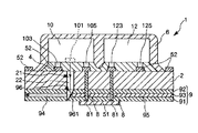
図1に示すように、本発明により製造された光導波路を有する光導波路構造体1は、光導波路9と、光導波路9の両面にそれぞれ接合された導体層51、52と、光導波路9の光路を屈曲させる光路変換部96と、発光素子10と、電気素子12とを備えている。
<First Embodiment: FIG. 1>
As shown in FIG. 1, an optical waveguide structure 1 having an optical waveguide manufactured according to the present invention includes an
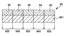
光導波路9は、図1中下側からクラッド層91、コア層93およびクラッド層92をこの順に積層してなるものであり、コア層93には、所定パターンのコア部94とクラッド部95とが形成されている。コア部94は、伝送光の光路を形成する部分であり、クラッド部95は、コア層93に形成されているものの伝送光の光路を形成せず、クラッド層91、92と同様の機能を果たす部分である。
The
図1に示す構成では、コア層93の後述する反射面961より図1中左側の部位は、コア部94が形成され、コア層93のそれ以外の部分は、クラッド部95が形成されている。
In the configuration shown in FIG. 1, a
コア層93の構成材料としては、活性放射線(活性エネルギー光線、電子線またはX線等)の照射により、あるいはさらに加熱することにより屈折率が変化する材料とされる。このような材料の好ましい例としては、ベンゾシクロブテン系樹ポリマー、ノルボルネン系ポリマー(樹脂)等の環状オレフィン系樹脂を含む樹脂組成物を主材料とするものが挙げられ、ノルボルネン系ポリマーを含む(主材料とする)ものが特に好ましい。
As a constituent material of the
このような材料で構成されたコア層93は、曲げ等の変形に対する耐性に優れ、特に繰り返し湾曲変形した場合でも、コア部94とクラッド部95との剥離や、コア層93と隣接する層(クラッド層91、92)との層間剥離が生じ難く、コア部94内やクラッド部95内にマイクロクラックが発生することも防止される。その結果、光導波路9の光伝送性能が維持され、耐久性に優れた光導波路9が得られる。
The
また、コア層93の構成材料には、例えば、酸化防止剤、屈折率調整剤、可塑剤、増粘剤、補強剤、増感剤、レベリング剤、消泡剤、密着助剤および難燃剤等の添加剤が含まれていてもよい。酸化防止剤の添加は、高温安定性の向上、耐候性の向上、光劣化の抑制という効果がある。このような酸化防止剤としては、例えば、モノフェノール系、ビスフェノール系、トリフェノール系等のフェノール系や、芳香族アミン系のものが挙げられる。また、可塑剤、増粘剤、補強剤の添加により、曲げに対する耐性をさらに増大させることもできる。
Examples of the constituent material of the
前記酸化防止剤に代表される添加剤の含有率(2種以上の場合は合計)は、コア層93の構成材料全体に対し、0.5〜40重量%程度が好ましく、3〜30重量%程度がより好ましい。この量が少なすぎると、添加剤の機能を十分に発揮することができず、量が多すぎると、添加剤の種類や特性によっては、コア部94を伝送する光(伝送光)の透過率の低下、パターニング不良、屈折率不安定等を生じるおそれがある。
The content of additives typified by the antioxidant (the total in the case of two or more) is preferably about 0.5 to 40% by weight, and 3 to 30% by weight with respect to the entire constituent material of the
コア層93の形成方法としては、塗布法が挙げられる。塗布法としては、コア層形成用組成物(ワニス等)を塗布し硬化(固化)させる方法、硬化性を有するモノマー組成物を塗布し硬化(固化)させる方法が挙げられる。また、塗布法以外の方法、例えば、別途製造されたシート材を接合する方法を採用することもできる。
An example of a method for forming the
以上のようにして得られたコア層93に対し、マスクを用いて活性放射線を選択的に照射し、所望の形状のコア部94をパターニングする。
The
露光に用いる活性放射線としては、可視光、紫外光、赤外光、レーザ光等の活性エネルギー光線や電子線、X線等が挙げられる。電子線は、例えば50〜2000KGy程度の照射量で照射することができる。 Examples of the active radiation used for exposure include active energy rays such as visible light, ultraviolet light, infrared light, and laser light, electron beams, and X-rays. The electron beam can be irradiated with an irradiation amount of, for example, about 50 to 2000 KGy.
コア層93において、活性放射線が照射された部位は、その屈折率が変化し(コア層93の材料により、屈折率が増大する場合と減少する場合とがある)、活性放射線が照射されなかった部位との間で屈折率の差が生じる。例えば、コア層93の活性放射線が照射された部位がクラッド部954となり、照射されなかった部位がコア部94となる。また、この逆の場合もある。クラッド部95の屈折率は、クラッド層91、92の屈折率とほぼ等しい。
In the
また、コア層93に対し活性放射線を所定のパターンで照射した後、加熱することにより、コア部94を形成する場合もある。この加熱工程を付加することにより、コア部94とクラッド部95との屈折率の差がより大きくなるので好ましい。なお、この原理等については、後に詳述する。
Moreover, the
形成されるコア部94のパターン形状としては、特に限定されず、直線状、湾曲部を有する形状、異形、光路の分岐部、合流部または交差部を有する形状、集光部(幅等が減少している部分)または光拡散部(幅等が増大している部分)、あるいはこれらのうちの2以上を組み合わせた形状等、いかなるものでもよい。活性放射線の照射パターンの設定により、いかなる形状のコア部94をも容易に形成することができる点が、本発明の特徴である。
The pattern shape of the
光導波路9の各部の構成材料およびコア部94の形成方法等については、後に詳述する。
The constituent material of each part of the
光導波路9の下面に接合された導体層51および上面に接合された導体層52は、それぞれ、所定の形状にパターンニングされて、所望の配線または回路を構成している。導体層51、52の構成材料としては、例えば、銅、銅系合金、アルミニウム、アルミニウム系合金等の各種金属材料が挙げられる。導体層51、52の厚さは、特に限定されないが、通常、3〜120μm程度が好ましく、5〜70μm程度がより好ましい。
The
導体層51、52は、例えば、金属箔の接合(接着)、金属メッキ、蒸着、スパッタリング等の方法により形成されたものである。導体層51、52へのパターニングは、例えばエッチング、印刷、マスキング等の方法を用いることができる。 The conductor layers 51 and 52 are formed by methods such as bonding (adhesion) of metal foil, metal plating, vapor deposition, sputtering, and the like. For example, etching, printing, masking, or the like can be used for patterning the conductor layers 51 and 52.
発光素子10は、図1中下面側に、発光部101と、一対の端子103、105とを有している。発光部101は、端子103と端子105の間に位置している。端子103、105間に通電がなされると、発光部101が発光する。
The
なお、発光素子10における発光部は、1つの発光点で構成されているものの他、発光点が複数個集合したものでもよい。発光点が複数個集合したものとしては、例えば、発光点が列状(例えば発光点が1×4個、1×12個)または行列状(例えば発光点がn×m個:n、mは2以上の整数)に配置されたものや、複数の発光点がランダム(不規則)に配置されたもの等が挙げられる。後述する受光素子11における受光部111についても同様である。
In addition, the light emitting part in the
発光素子10は、それらの端子103、105がそれぞれ導体層52の所定部位に接合(電気的に接続)されるようにして光導波路9上に搭載されている。
The
電気素子(電子回路素子)12は、例えば半導体素子(半導体チップ)で構成されている。電気素子12の機能は特に限定されないが、一例として、発光素子10を駆動するための回路を構成するものが挙げられる。この電気素子12は、図1中下面側に、2つの端子123、125を有している。
The electric element (electronic circuit element) 12 is composed of, for example, a semiconductor element (semiconductor chip). Although the function of the
電気素子12は、それらの端子123、125がそれぞれ導体層52の所定部位に接合(電気的に接続)されるようにして光導波路9上に搭載されている。
The
発光素子10および電気素子12は、それらの端子103、105、123、125を含む下部がアンダーフィル材4により封止されている。これにより、発光素子10および電気素子12と、光導波路9との間には、空隙部が形成されることなくアンダーフィル材4により封止されることとなる。さらに、発光素子10および電気素子12は、その全体(外表面)が封止材6により覆われ、封止されている。このように、発光素子10および電気素子12は、その全体が封止され、特に発光部101が外部に露出することなく封止された構造であるため、汚れ、損傷、酸化劣化等から保護され、電子部品の信頼性向上に寄与する。
The lower part including the
アンダーフィル材4は、発光部101から発せられる光(伝送光)を実質的に透過する材料で構成されており、好ましくは、透明な材料で構成されている。
The
アンダーフィル材4の構成材料としては、絶縁性を有する樹脂材料が好ましく、例えば、エポキシ樹脂、フェノール樹脂、ウレタン樹脂、ポリイミド樹脂等が挙げられる。
As a constituent material of the
また、封止材6の構成材料としては、絶縁性を有する樹脂材料が好ましく、例えば、エポキシ樹脂、フェノール樹脂、ノルボルネン樹脂、シリコン樹脂等が挙げられる。
Moreover, as a constituent material of the sealing
図1に示すように、光導波路9には、その厚さ方向に貫通する4つの貫通孔(スルーホール)8が形成されている。各貫通孔8には、導電材料(例えば、銅、銅系合金、アルミニウム、アルミニウム系合金等の各種金属材料)が充填され、導体ポスト81を形成している。これらの導体ポスト81を介して、導体層51と導体層52の所定部位同士が導通している。すなわち、発光素子10および電気素子12の端子103、105、123、125への通電は、光導波路9の下面側の導体層51を介して行うことができるようになっている。なお、端子105と端子123とは導通し、これらはグランド側に接続されている。
As shown in FIG. 1, the
光導波路9のコア部94は、平面視で(図1の上方から見たとき)発光素子10の発光部101と重なるような(すなわち、発光部101の真下を通過するような)パターン形状で形成されている。このコア部94は、クラッド部95に比べて屈折率が高く、また、クラッド層91、92に対しても屈折率が高い。クラッド層91および92は、それぞれ、コア部94の下部および上部に位置するクラッド部を構成するものである。このような構成により、コア部94は、その外周の全周をクラッド部に囲まれた導光路として機能する。
The
このような光導波路9は、コア部94の光路を屈曲させる光路変換部96を有している。この光路変換部96は、伝送光の少なくとも一部を反射する反射面(ミラー)961で構成されている。この反射面961は、発光部101の真下の位置に設けられている。
Such an
反射面961は、光導波路9の光路、すなわちコア部94の長手方向に対しほぼ45°傾斜しており、伝送光の大半(例えば90%以上)を反射する機能を有している。
The reflecting
このような光路変換部96は、光導波路9の一部を除去(欠損)することにより例えば断面が下方を底辺とする三角形の凹部を形成し、その1つの傾斜面を反射面961として用いるものである。反射面961は、例えば多層光学薄膜や金属薄膜(例えばアルミ蒸着膜)のような反射膜あるいは反射増加膜を有していてもよい。また、図示しないが、光路変換部96の凹部には、充填材、特にコア部94と屈折率の異なる充填材が充填されていてもよい。
Such an optical
図示の構成では、反射面961(光路変換部96)は、コア層93とクラッド層92とにまたがって形成されているが、コア層93内のみに形成されていてもよい。
In the configuration shown in the figure, the reflection surface 961 (the optical path conversion unit 96) is formed across the
本実施形態の光導波路構造体1では、導体層51、導体ポスト81および導体層52を介して発光素子10の端子103、105間へ通電がなされると、発光部101が点灯し、図1中下方へ向かって発せられた光は、アンダーフィル材4およびクラッド層92を順次透過し、反射面961で反射されて90°屈曲し、光導波路9のコア部94に入り、クラッド部(クラッド層91、92および側方のクラッド部95)との界面で反射を繰り返しながら、コア部94内をその長手方向(図1中左方向)に沿って進む。
In the optical waveguide structure 1 of the present embodiment, when power is applied between the
また、導体層51、導体ポスト81および導体層52を介して電気素子12の端子123、125間へ通電がなされると、電気素子12が駆動する。
Further, when energization is performed between the
なお、図1では、図中最も左側にある導体ポスト81とコア部94とが交差しているように示されているが、これらは図1の紙面の前後方向にずれており、コア部94の光路は、導体ポスト81と干渉しないようになっている。
In FIG. 1, the
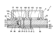
<第2実施形態:図2>
図2には、本発明により製造された光導波路を有する光導波路構造体1の第2実施形態が示されている。以下、この光導波路構造体1について説明するが、前記第1実施形態と同様の事項についてはその説明を省略し、相違点を中心に説明する。
Second Embodiment: FIG. 2
FIG. 2 shows a second embodiment of an optical waveguide structure 1 having an optical waveguide manufactured according to the present invention. Hereinafter, although this optical waveguide structure 1 is demonstrated, the description is abbreviate | omitted about the matter similar to the said 1st Embodiment, and it demonstrates centering around difference.
本実施形態の光導波路構造体1は、光路変換部96の構成が前記と異なり、それ以外は同様である。すなわち、光路変換部96を構成する反射面(ミラー)961は、発光部101の真下の位置しているが、この反射面961は、クラッド層91とコア層93とクラッド層92の3層にまたがって形成されている。すなわち、光路変換部96の三角形の凹部は、光導波路9の下面に開放している。
In the optical waveguide structure 1 of the present embodiment, the configuration of the optical
なお、反射面961が、多層光学薄膜や金属薄膜のような反射膜あるいは反射増加膜を有していてもよいことや、光路変換部96の凹部に、充填材が充填されていてもよいことは、前記と同様である。
The
<第3実施形態:図3>
図3には、本発明により製造された光導波路を有する光導波路構造体1の第3実施形態が示されている。以下、この光導波路構造体1について説明するが、前記第1実施形態と同様の事項についてはその説明を省略し、相違点を中心に説明する。
<Third Embodiment: FIG. 3>
FIG. 3 shows a third embodiment of an optical waveguide structure 1 having an optical waveguide manufactured according to the present invention. Hereinafter, although this optical waveguide structure 1 is demonstrated, the description is abbreviate | omitted about the matter similar to the said 1st Embodiment, and it demonstrates centering around difference.
本実施形態の光導波路構造体1は、基板2を有し、この基板2の下面に接着層3を介して光導波路9が接着されている。基板2は、アンダーフィル材4と同様に、発光部101から発せられる光(伝送光)を実質的に透過する材料(伝送光に対する透光性を有する材料)で構成されており、好ましくは、実質的に透明な材料で構成された透明基板である。
The optical waveguide structure 1 of this embodiment has a
詳述すると、基板2の光学的特性は、伝送光の透過率が80%以上であるのが好ましく、90%以上であるのがより好ましく、95%以上であるのがさらに好ましい。基板2がこのような光学的特性を有することから、基板2における発光部101の真下の部位は、伝送光を透光する透光部21を構成している。
More specifically, the optical characteristics of the
接着層3についても同様に、発光部101から発せられる伝送光を実質的に透過する材料で構成されており、好ましくは、透明な材料で構成されている。
Similarly, the adhesive layer 3 is made of a material that substantially transmits the transmission light emitted from the
基板2の構成材料としては、例えば、エポキシ樹脂、フェノール樹脂、ビスマレイミド樹脂、ビスマレイミド・トリアジン樹脂、トリアゾール樹脂、ポリシアヌレート樹脂、ポリイソシアヌレート樹脂、ベンゾシクロブテン樹脂、ポリイミド樹脂、ポリベンザオキサゾール樹脂、ノルボルネン樹脂等が挙げられる。また、これらの材料は、単独で使用してもよく、複数を混合して使用してもよい。
また、基板2は、例えばガラス繊維、樹脂繊維等の繊維基材(織布、不織布、織物、編物等)に前述したような樹脂材料を含浸させたもの(プリプレグ等)であってもよい。例えば、ガラスクロスにエポキシ樹脂を含浸させたものをガラスエポキシ基板と言うが、このようなものを基板2として用いることができる。このような繊維基材を含む基板2は、比較的薄くても高強度で、また、熱膨張率も低いため、基板2に光導波路9や導体層(金属層)を接合した場合に特に有利である。
また、基板2は、複数の層の積層体であってもよい。例えば、それぞれ組成(種類)が異なる樹脂材料からなる第1の層と第2の層とを積層したもの、前記繊維基材に樹脂材料を含浸させた層(シート材)と、樹脂材料からなる層とを積層したものが挙げられる。なお、積層体における層構成は、これに限定されないことは言うまでもない。
Examples of the constituent material of the
Further, the
Moreover, the board |
基板2の厚さは、特に限定されないが、通常、50μm〜1.2mm程度が好ましく、100〜600μm程度がより好ましい。
Although the thickness of the board |
基板2は、硬質(リジッド)のものでも、可撓性(フレキシブル)を有するものでもよい。また、硬質の基板と可撓性を有する基板の双方を有していてもよい。この場合、光導波路9は、硬質の基板と可撓性を有する基板の少なくとも一方に形成されていればよく、双方にまたがって形成されていてもよい。
The
接着層3としては、シート材(ボンディングシート)を用いることができ、その構成材料としては、例えば、エポキシ系接着剤、アクリル系接着剤、フェノール樹脂系接着剤、シアネート樹脂系接着剤、マレイミド樹脂系接着剤等が挙げられる。特に、酸化防止等のために、フラックス活性を有する材料で構成されているのが好ましい。 As the adhesive layer 3, a sheet material (bonding sheet) can be used, and examples of the constituent material thereof include an epoxy adhesive, an acrylic adhesive, a phenol resin adhesive, a cyanate resin adhesive, and a maleimide resin. System adhesives and the like. In particular, it is preferably made of a material having flux activity for preventing oxidation or the like.
接着層3としてシート材を用いず、基板2の下面または光導波路9の上面に塗膜による接着層3を形成してもよい。また、接着層3は、2層以上を積層したものでもよい。
The adhesive layer 3 may be formed by a coating film on the lower surface of the
接着層3の厚さは、特に限定されないが、0.5〜150μm程度が好ましく、10〜70μm程度がより好ましい。 Although the thickness of the contact bonding layer 3 is not specifically limited, About 0.5-150 micrometers is preferable and about 10-70 micrometers is more preferable.
導体層52は、基板2の上面に形成されている。この場合、導体層52の一部は、封止材6より外方に露出している。また、光導波路9の下面に形成された導体層51は、前記第1実施形態のそれとは配線パターンが異なっている。
The
図3に示すように、2つの導体ポスト81が光導波路9、接着層3および基板2を貫通して設けられており、これらの導体ポスト81を介して、導体層51と導体層52の所定部位同士が導通している。すなわち、発光素子10の端子105と、電気素子12の端子123とが、導体層51、導体ポスト81および導体層52を介して導通し、これらはグランド側に接続されている。
As shown in FIG. 3, two
封止材6より外方に露出した一方の導体層52と導体層51との間に通電すると、発光部101が発光し、封止材6より外方に露出した他方の導体層52と導体層51との間に通電すると、電気素子12が駆動する。
When a current is applied between one
本実施形態の光導波路構造体1では、導体層51、導体ポスト81および導体層52を介して発光素子10の端子103、105間へ通電がなされると、発光部101が点灯し、図3中下方へ向かって発せられた光は、アンダーフィル材4、基板2(基板2の透光部)、接着層3およびクラッド層92を順次透過し、反射面961で反射されて90°屈曲し、光導波路9のコア部94に入り、クラッド部(クラッド層91、92および側方のクラッド部95)との界面で反射を繰り返しながら、コア部94内をその長手方向(図3中左方向)に沿って進む。
In the optical waveguide structure 1 of the present embodiment, when power is applied between the
<第4実施形態:図4>
図4には、本発明により製造された光導波路を有する光導波路構造体1の第4実施形態が示されている。以下、この光導波路構造体1について説明するが、前記第1および第3実施形態と同様の事項についてはその説明を省略し、相違点を中心に説明する。
<Fourth Embodiment: FIG. 4>
FIG. 4 shows a fourth embodiment of an optical waveguide structure 1 having an optical waveguide manufactured according to the present invention. Hereinafter, although this optical waveguide structure 1 is demonstrated, the description is abbreviate | omitted about the matter similar to the said 1st and 3rd embodiment, and it demonstrates centering around difference.
本実施形態の光導波路構造体1は、接着層3を有さず、基板2と光導波路9とが直接接合されている点、および光路変換部96の構成が異なる点を除き、前記第3実施形態と同様である。基板2と光導波路9とが直接接合されているため、光導波路構造体1の薄型化に寄与する。
The optical waveguide structure 1 of this embodiment does not have the adhesive layer 3, except that the
光路変換部96を構成する反射面(ミラー)961は、発光部101の真下の位置しているが、この反射面961は、クラッド層91とコア層93とクラッド層92の3層にまたがって形成されている。すなわち、光路変換部96は、上方を底辺とする三角形の凹部で構成され、その斜面に反射面961が形成されている。このような光路変換部96は、基板2に隣接して設けられている。
The reflection surface (mirror) 961 constituting the optical
なお、反射面961が、多層光学薄膜や金属薄膜のような反射膜あるいは反射増加膜を有していてもよいことや、光路変換部96の凹部に、充填材が充填されていてもよいことは、前記と同様である。
The
本実施形態の光導波路構造体1では、導体層51、導体ポスト81および導体層52を介して発光素子10の端子103、105間へ通電がなされると、発光部101が点灯し、図4中下方へ向かって発せられた光は、アンダーフィル材4および基板2を順次透過し、反射面961で反射されて90°屈曲し、光導波路9のコア部94に入り、クラッド部(クラッド層91、92および側方のクラッド部95)との界面で反射を繰り返しながら、コア部94内をその長手方向(図4中左方向)に沿って進む。
In the optical waveguide structure 1 of the present embodiment, when the current is passed between the
<第5実施形態:図5>
図5には、本発明により製造された光導波路を有する光導波路構造体1の第5実施形態が示されている。以下、この光導波路構造体1について説明するが、前記第1および第3実施形態と同様の事項についてはその説明を省略し、相違点を中心に説明する。
<Fifth Embodiment: FIG. 5>
FIG. 5 shows a fifth embodiment of an optical waveguide structure 1 having an optical waveguide manufactured according to the present invention. Hereinafter, although this optical waveguide structure 1 is demonstrated, the description is abbreviate | omitted about the matter similar to the said 1st and 3rd embodiment, and it demonstrates centering around difference.
本実施形態の光導波路構造体1は、基板2の構成が異なり、それ以外は前記第3実施形態と同様である。すなわち、基板2は、伝送光の透過性を十分に有さないものであり、基板2における発光部101の真下の位置には、基板2を貫通する貫通孔22が形成されている。この貫通孔22は、伝送光を透光する透光部21を構成するものである。すなわち、この貫通孔22が、伝送光を基板2の厚さ方向に導光(伝送)する導光路となる。
The optical waveguide structure 1 of the present embodiment is the same as the third embodiment except for the configuration of the
なお、図示されていないが、貫通孔22の内部(全部または一部)に、伝送光の透過率が80%以上、好ましくは90%以上、より好ましくは95%以上の材料による充填材が充填されていてもよい。また、図示されていないが、貫通孔22の内面等に導電材料による層を形成することによって、光伝送機能の他に、電気信号を伝送する機能を持たせてもよい。
Although not shown in the drawing, the inside (all or a part) of the through-
本実施形態の光導波路構造体1では、導体層51、導体ポスト81および導体層52を介して発光素子10の端子103、105間へ通電がなされると、発光部101が点灯し、図5中下方へ向かって発せられた光は、アンダーフィル材4を透過し、貫通孔22内を通り、接着層3およびクラッド層92を透過し、反射面961で反射されて90°屈曲し、光導波路9のコア部94に入り、クラッド部(クラッド層91、92および側方のクラッド部95)との界面で反射を繰り返しながら、コア部94内をその長手方向(図5中左方向)に沿って進む。
In the optical waveguide structure 1 of the present embodiment, when power is applied between the
<第6実施形態:図6>
図6には、本発明により製造された光導波路を有する光導波路構造体1の第6実施形態が示されている。以下、この光導波路構造体1について説明するが、前記第1、第4および第5実施形態と同様の事項についてはその説明を省略し、相違点を中心に説明する。
<Sixth Embodiment: FIG. 6>
FIG. 6 shows a sixth embodiment of an optical waveguide structure 1 having an optical waveguide manufactured according to the present invention. Hereinafter, although this optical waveguide structure 1 is demonstrated, the description is abbreviate | omitted about the matter similar to the said 1st, 4th and 5th embodiment, and it demonstrates centering around difference.
本実施形態の光導波路構造体1は、前記第4実施形態の光導波路構造体1において、基板2を、前記第5実施形態の基板2に置き換えたものである。すなわち、本実施形態の光導波路構造体1における基板2は、伝送光の透過性を十分に有さないものであり、発光部101の真下の位置に、基板2を貫通する貫通孔(基板2の厚さ方向の導光路)22が形成されている。この貫通孔22は、透光部21を構成するものである。
The optical waveguide structure 1 of this embodiment is obtained by replacing the
本実施形態の光導波路構造体1では、導体層51、導体ポスト81および導体層52を介して発光素子10の端子103、105間へ通電がなされると、発光部101が点灯し、図6中下方へ向かって発せられた光は、アンダーフィル材4を透過し、貫通孔22内を通り、反射面961で反射されて90°屈曲し、光導波路9のコア部94に入り、クラッド部(クラッド層91、92および側方のクラッド部95)との界面で反射を繰り返しながら、コア部94内をその長手方向(図6中左方向)に沿って進む。
In the optical waveguide structure 1 of the present embodiment, when power is supplied between the
<第7実施形態:図7>
図7には、本発明により製造された光導波路を有する光導波路構造体1の第7実施形態が示されている。以下、この光導波路構造体1について説明するが、前記第1および第5実施形態と同様の事項についてはその説明を省略し、相違点を中心に説明する。
<Seventh Embodiment: FIG. 7>
FIG. 7 shows a seventh embodiment of an optical waveguide structure 1 having an optical waveguide manufactured according to the present invention. Hereinafter, although this optical waveguide structure 1 is demonstrated, the description is abbreviate | omitted about the matter similar to the said 1st and 5th embodiment, and it demonstrates centering around difference.
本実施形態の光導波路構造体1は、基板2の透光部(厚さ方向に形成された導光路)21の構成が前記第5実施形態と異なり、その他は第5実施形態と同様である。すなわち、基板2の発光部101の真下の位置に形成された貫通孔22内には、コア部24と、該コア部24の外周を囲むクラッド部25とで構成された垂直光導波路23が挿入されている。
The optical waveguide structure 1 of the present embodiment is different from the fifth embodiment in the configuration of the light transmitting part (light guide path formed in the thickness direction) 21 of the
コア部24の構成材料や形成方法は、コア部94と同様とすることができる。あるいは、コア部24は、前記第5実施形態において述べた貫通孔22内への充填材と同様のものを用いてもよい。クラッド部25の構成材料は、クラッド部95またはクラッド層91、92と同様とすることができる。
The constituent material and the forming method of the
本実施形態の光導波路構造体1では、導体層51、導体ポスト81および導体層52を介して発光素子10の端子103、105間へ通電がなされると、発光部101が点灯し、図7中下方へ向かって発せられた光は、アンダーフィル材4を透過し、垂直光導波路23のコア部24内を通り、接着層3およびクラッド層92を透過し、反射面961で反射されて90°屈曲し、光導波路9のコア部94に入り、クラッド部(クラッド層91、92および側方のクラッド部95)との界面で反射を繰り返しながら、コア部94内をその長手方向(図7中左方向)に沿って進む。
In the optical waveguide structure 1 of the present embodiment, when the current is passed between the
<第8実施形態:図8>
図8には、本発明により製造された光導波路を有する光導波路構造体1の第8実施形態が示されている。以下、この光導波路構造体1について説明するが、前記第1および第6実施形態と同様の事項についてはその説明を省略し、相違点を中心に説明する。
<Eighth embodiment: FIG. 8>
FIG. 8 shows an eighth embodiment of an optical waveguide structure 1 having an optical waveguide manufactured according to the present invention. Hereinafter, although this optical waveguide structure 1 is demonstrated, the description is abbreviate | omitted about the matter similar to the said 1st and 6th embodiment, and it demonstrates centering around difference.
本実施形態の光導波路構造体1は、前記第6実施形態の光導波路構造体1において、基板2の厚さ方向に形成された導光路の構成を第7実施形態のそれと同様としたものである。すなわち、基板2の発光部101の真下の位置に形成された貫通孔22内には、コア部24と、該コア部24の外周を囲むクラッド部25とで構成された垂直光導波路23が挿入されている。
The optical waveguide structure 1 of the present embodiment is the same as that of the seventh embodiment in the configuration of the light guide formed in the thickness direction of the
本実施形態の光導波路構造体1では、導体層51、導体ポスト81および導体層52を介して発光素子10の端子103、105間へ通電がなされると、発光部101が点灯し、図8中下方へ向かって発せられた光は、アンダーフィル材4を透過し、垂直光導波路23のコア部24内を通り、反射面961で反射されて90°屈曲し、光導波路9のコア部94に入り、クラッド部(クラッド層91、92および側方のクラッド部95)との界面で反射を繰り返しながら、コア部94内をその長手方向(図8中左方向)に沿って進む。
In the optical waveguide structure 1 of the present embodiment, when the current is passed between the
<第9実施形態:図9>
図9には、本発明により製造された光導波路を有する光導波路構造体1の第9実施形態が示されている。以下、この光導波路構造体1について説明するが、前記第1および第8実施形態と同様の事項についてはその説明を省略し、相違点を中心に説明する。
<Ninth Embodiment: FIG. 9>
FIG. 9 shows a ninth embodiment of an optical waveguide structure 1 having an optical waveguide manufactured according to the present invention. Hereinafter, although this optical waveguide structure 1 is demonstrated, the description is abbreviate | omitted about the matter similar to the said 1st and 8th embodiment, and it demonstrates centering around difference.
本実施形態の光導波路構造体1は、透光部21に、伝送光を集光または拡散し得るレンズ部26を設けた以外は、前記第8実施形態と同様のものである。すなわち、垂直光導波路23の上端面(入射側)に凸レンズ(正確には、平凸レンズ)で構成されるレンズ部26が設けられている。
The optical waveguide structure 1 of the present embodiment is the same as that of the eighth embodiment except that the
これにより、発光部101から図9中下方へ向かって発せられた光は、アンダーフィル材4を透過した後、レンズ部26で集光されてその光束(ビーム)が絞られ、この光束が垂直光導波路23のコア部24内を通り、反射面961で反射されて90°屈曲し、光導波路9のコア部94に入り、コア部94内をその長手方向(図9中左方向)に沿って進む。このようなレンズ部26を設けることにより、より明確な(シャープな)伝送光を得ることができ、より優れた光伝送特性を得ることができる。
As a result, the light emitted downward from the
なお、レンズ部26は、伝送光を拡散し得るものでもよい。この場合には、凹レンズを用いればよい。
The
また、レンズ部26の設置位置は、図9に示す位置に限らず、例えば透光部21の途中や下部であってもよく、あるいは、その他の箇所、例えばコア部94の入射側端部や出射側端部であってもよい。
In addition, the installation position of the
<第10実施形態:図10>
図10には、本発明により製造された光導波路を有する光導波路構造体1の第10実施形態が示されている。以下、この光導波路構造体1について説明するが、前記第1、第2実施形態等と同様の事項についてはその説明を省略し、相違点を中心に説明する。
<Tenth Embodiment: FIG. 10>
FIG. 10 shows a tenth embodiment of an optical waveguide structure 1 having an optical waveguide manufactured according to the present invention. Hereinafter, although this optical waveguide structure 1 is demonstrated, the description is abbreviate | omitted about the matter similar to the said 1st, 2nd embodiment, etc., and it demonstrates centering around difference.
クラッド層91、92とそれらの間に位置する(介挿された)コア層93とで構成された光導波路9の下面および上面には、それぞれ、所定のパターン形状の導体層51および52が接合されており、導体層51および導体層52の所定の部位同士は、光導波路9を貫通して形成された2つの導体ポスト81によりそれぞれ電気的に接続されている。
また、光導波路9には、2つの光路変換部96a、96bが形成されている。これらの光路変換部96a、96bは、それぞれ、前記と同様の反射面961a、961bを有している。光導波路9において、コア層93の反射面961aより図10中左側および反射面961bより図10中右側の部位は、コア部94が形成され、コア層93のそれ以外の部分は、クラッド部95が形成されている。
In addition, two optical
このような光導波路9の上部には、チップキャリア(素子)13が搭載されている。チップキャリア13は、基板2’と、光導波路9とは別の光導波路9’と、発光素子10と、受光素子11と、導体層54、55と、電気素子12とを備えている。以下、チップキャリア13の構成について詳述する。
A chip carrier (element) 13 is mounted on the
基板2’の下面には、クラッド層91、92とそれらの間に位置する(介挿された)コア層93とで構成された光導波路9’が接合されており、光導波路9’の下面および基板2’の上面には、それぞれ、所定のパターン形状の導体層54および55が接合されている。導体層54、55の構成材料、形成方法、パターニング方法等については、前記導体層51、52と同様である。
An
基板2’は、実質的に透明のものでも、不透明のものでもよく、また、硬質(リジッド)のものでも、可撓性(フレキシブル)を有するものでもよい。 The substrate 2 'may be substantially transparent or opaque, and may be rigid (rigid) or flexible (flexible).
導体層54および導体層55の所定の部位同士は、基板2’および光導波路9’を貫通して形成された4つの導体ポスト82によりそれぞれ電気的に接続されている。
Predetermined portions of the
また、光導波路9’には、4つの光路変換部96c、96d、96e、96fが形成されている。これらの光路変換部96c、96d、96e、96fは、それぞれ、前記と同様の反射面961c、961d、961e、961fを有している。
Further, four optical
光導波路9’において、コア層93の反射面961cと反射面961dとの間の部位、および反射面961eと反射面961fとの間の部位は、コア部94が形成され、コア層93のそれ以外の部分は、クラッド部95が形成されている。
In the
基板2’の上部には、4つの端子123、125、127、129を備える電気素子(半導体素子)12が搭載されている。電気素子12は、それらの端子123、125、127、129がそれぞれ導体層55の所定部位に接合(電気的に接続)されるようにして基板2’上に搭載されている。
An electric element (semiconductor element) 12 including four
電気素子12の機能は特に限定されないが、一例として、発光素子10を駆動するための回路を構成するものが挙げられる。また、電気素子12は、さらに、受光素子11が出力した電気信号を処理(例えば信号の増幅)する機能(回路)を備えていてもよい。
Although the function of the
このような電気素子12は、その全体(外表面)が前記封止材6と同様の封止材61により覆われ、封止されている。
Such an
光導波路9’の下部には、発光素子10および受光素子11が搭載されている。発光素子10は、前記と同様のものである。受光素子11は、図10中上面側に、受光部111と、一対の端子113、115とを有している。受光部111は、端子113と端子115の間に位置している。受光部111が受光する(伝送光が照射される)と、その光が光電変換され、端子113、115間に電位差が生じ、電気信号が出力される。
A
発光素子10は、それらの端子103、105がそれぞれ導体層54の所定部位に接合(電気的に接続)されるようにして光導波路9’の下部に搭載されている。受光素子11は、それらの端子113、115がそれぞれ導体層54の所定部位に接合(電気的に接続)されるようにして光導波路9’の下部に搭載されている。
The
発光素子10および受光素子11は、それらの端子103、105、113、115を含む上部がアンダーフィル材4により封止されており、さらに、発光素子10および受光素子11の全体(外表面)が封止材6により覆われ、封止されている。
The
光導波路9’のコア部94は、平面視で(図10の上方から見たとき)発光素子10の発光部101と重なるとともに受光素子11の受光部111と重なるような(すなわち、発光部101の真上および受光部111の真上を通過するような)パターン形状で形成されている。
The
また、反射面961dは、発光部101の真上の位置に設けられ、反射面961eは、受光部111の真上の位置に設けられ、反射面961cは、反射面961aの真上の位置に設けられ、反射面961fは、反射面961bの真上の位置に設けられている。
The
このようなチップキャリア13は、導体層52と導体層54の所定部位同士が半田(半田ボール)7により電気的に接続されるようにして光導波路9上に搭載されている。この場合、光導波路9、9’間は、前記アンダーフィル材4と同様のアンダーフィル材41により封止されている。
Such a
導体層52の一部は、アンダーフィル材41により封止され、導体層52の一部は、アンダーフィル材41で封止されずに外部に露出している。
A part of the
本実施形態の光導波路構造体1では、発光素子10の端子103、105間へ通電がなされると、発光部101が点灯し、図10中上方へ向かって発せられた光は、アンダーフィル材4を透過し、反射面961dで反射されて90°屈曲し、光導波路9’のコア部94に入り、コア部94内をその長手方向(図10中左方向)に沿って進む。さらに、コア部94の端部から出射した伝送光は、反射面961cで反射されて90°屈曲し、下方へ向かい、アンダーフィル材41およびクラッド層92を透過し、反射面961aで反射されて90°屈曲し、光導波路9のコア部94に入り、コア部94内をその長手方向(図10中左方向)に沿って進む。
In the optical waveguide structure 1 of the present embodiment, when power is supplied between the
一方、光導波路9の図10中右側からコア部94に入った光は、コア部94内をその長手方向(図10中左方向)に沿って進み、反射面961bで反射されて90°屈曲し、上方へ向かい、クラッド層92およびアンダーフィル材41を透過し、反射面961fで反射されて90°屈曲し、光導波路9’のコア部94に入り、コア部94内をその長手方向(図10中左方向)に沿って進む。さらに、コア部94の端部から出射した伝送光は、反射面961eで反射されて90°屈曲し、下方へ向かい、アンダーフィル材4を透過して受光部111で受光される。これにより、端子113、115間に電位差が生じ、電気信号が出力される。
On the other hand, the light that enters the
<第11実施形態:図11>
図11には、本発明により製造された光導波路を有する光導波路構造体1の第11実施形態が示されている。以下、この光導波路構造体1について説明するが、前記第1、第6および第10実施形態等と同様の事項についてはその説明を省略し、相違点を中心に説明する。
<Eleventh embodiment: FIG. 11>
FIG. 11 shows an eleventh embodiment of an optical waveguide structure 1 having an optical waveguide manufactured according to the present invention. Hereinafter, although this optical waveguide structure 1 is demonstrated, the description is abbreviate | omitted about the matter similar to the said 1st, 6th, 10th Embodiment, etc., and it demonstrates centering around difference.
基板2の下面には、クラッド層91、92とそれらの間に位置する(介挿された)コア層93とで構成された光導波路9が接合されており、基板2の上面には、所定のパターン形状の導体層52が接合されている。
An
また、光導波路9には、2つの光路変換部96a、96bが形成されている。光路変換部96aおよび96bは、前記第4、第8、第9実施形態における光路変換部96と同様の構成であり、それぞれ、前記と同様の反射面961a、961bを有している。
In addition, two optical
光導波路9において、コア層93の反射面961aより図11中左側および反射面961bより図11中右側の部位は、コア部94が形成され、コア層93のそれ以外の部分は、クラッド部95が形成されている。
In the
基板2は、伝送光の透過性(透光性)を十分に有さないものであり、基板2における反射面961a、961bの真上の位置(反射面961c、961fの真下の位置)には、それぞれ、基板2を貫通する貫通孔22が形成されている。これらの貫通孔22は、伝送光を透光する透光部21を構成するものである。すなわち、これらの貫通孔22が、伝送光を基板2の厚さ方向に導光(伝送)する導光路となる。
The
また、両貫通孔22(透光部21)の上部には、それぞれ、前記第9実施形態と同様のレンズ部26が設けられている。例えば、貫通孔22内に比較的屈折率の低い透明な第1の樹脂材料を充填し、その上面を湾曲凹面に形成し、該凹面内に前記第1の樹脂材料より高屈折率の透明な第2の樹脂材料を充填することにより、前記第2の樹脂材料の部分が凸レンズ(平凸レンズ、両凸レンズ等)として機能するレンズ部26を形成することができる。また、これに限らず、貫通孔22内に凸レンズ(平凸レンズ、両凸レンズ等)のみを設置してもよい。
Moreover, the
また、貫通孔22(透光部21)に対するレンズ部26の設置位置は、図示のような上部に限らず、貫通孔22の途中や下部であってもよい。
Moreover, the installation position of the
なお、図示されていないが、貫通孔22の内部(全部または一部)に、伝送光の透過率が80%以上、好ましくは90%以上、より好ましくは95%以上の材料による充填材が充填されていてもよい。また、前記第7、第8実施形態と同様に、貫通孔22の内部に垂直光導波路23が形成されていてもよい。
Although not shown in the drawing, the inside (all or a part) of the through-
このような基板2付きの光導波路9の上部には、前記第10実施形態と同様のチップキャリア(素子)13が搭載されている。
A chip carrier (element) 13 similar to that of the tenth embodiment is mounted on the top of the
本実施形態の光導波路構造体1では、発光素子10の端子103、105間へ通電がなされると、発光部101が点灯し、図11中上方へ向かって発せられた光は、アンダーフィル材4を透過し、反射面961dで反射されて90°屈曲し、光導波路9’のコア部94に入り、コア部94内をその長手方向(図11中左方向)に沿って進む。さらに、コア部94の端部から出射した伝送光は、反射面961cで反射されて90°屈曲し、下方へ向かい、アンダーフィル材41を透過した後、レンズ部26で集光されてその光束(ビーム)が絞られ、この光束が貫通孔22内を通り、反射面961aで反射されて90°屈曲し、光導波路9のコア部94に入り、コア部94内をその長手方向(図11中左方向)に沿って進む。
In the optical waveguide structure 1 of the present embodiment, when the current is applied between the
一方、光導波路9の図11中右側からコア部94に入った光は、コア部94内をその長手方向(図11中左方向)に沿って進み、反射面961bで反射されて90°屈曲し、貫通孔22内を上方へ向かい、レンズ部26で集光されてその光束(ビーム)が絞られ、この光束がアンダーフィル材41を透過し、反射面961fで反射されて90°屈曲し、光導波路9’のコア部94に入り、コア部94内をその長手方向(図11左方向)に沿って進む。さらに、コア部94の端部から出射した伝送光(集光された光束)は、反射面961eで反射されて90°屈曲し、下方へ向かい、アンダーフィル材4を透過して受光部111で受光される。これにより、端子113、115間に電位差が生じ、電気信号が出力される。
On the other hand, the light that enters the
以上、第1〜第11実施形態について説明したが、本発明はこれらに限定されるものではなく、発明の要旨を変更しない限り、他の構成のものでもよい。また、本発明は、第1〜第11実施形態のうちの任意の2以上の実施形態が備える構成を組み合わせたものでもよい。 The first to eleventh embodiments have been described above. However, the present invention is not limited to these, and other configurations may be used as long as the gist of the invention is not changed. Further, the present invention may be a combination of configurations included in any two or more of the first to eleventh embodiments.
次に、前記各実施形態における、光導波路9、9’の製造方法および各部の構成材料等について説明するが、特にコア部94の形成方法について詳細に説明する。
Next, the manufacturing method of the
<第1の製造方法>
まず、光導波路9の第1の製造方法について説明する。光導波路9’の製造方法は、光導波路9と同様であるため、光導波路9で代表する。
<First manufacturing method>
First, the 1st manufacturing method of the
図12−A〜図12−Eは、それぞれ、光導波路の第1の製造方法の工程例を模式的に示す断面図である。 FIGS. 12A to 12E are cross-sectional views schematically showing a process example of the first manufacturing method of the optical waveguide.
[1A] まず、支持基板951上に、層910を形成する(図12−A参照)。
層910は、コア層形成用材料(ワニス)900を塗布し硬化(固化)させる方法により形成される。
[1A] First, a
The
具体的には、層910は、支持基板951上にコア層形成用材料900を塗布して液状被膜を形成した後、この支持基板951を換気されたレベルテーブルに置いて、液状被膜表面の不均一な部分を水平化するとともに、溶媒を蒸発(脱溶媒)することにより形成する。
Specifically, the
層910を塗布法で形成する場合、例えば、ドクターブレード法、スピンコート法、ディッピング法、テーブルコート法、スプレー法、アプリケーター法、カーテンコート法、ダイコート法等の方法が挙げられるが、これらに限定されるわけではない。
When the
支持基板951には、例えば、シリコン基板、二酸化ケイ素基板、ガラス基板、石英基板、ポリエチレンテレフタレート(PET)フィルム等が用いられる。
As the
コア層形成用材料900は、ポリマー915と、添加剤920(本実施形態では、少なくともモノマー、助触媒および触媒前駆体を含む)とで構成される光誘発熱現像性材料(PITDM)を含有し、活性放射線の照射および加熱により、ポリマー915中において、モノマーの反応が生じる材料である。
The core
そして、得られた層910中では、ポリマー(マトリックス)915は、いずれも、実質的に一様かつランダムに分配され、添加剤920は、ポリマー915内に実質的に一様かつランダムに分散されている。これにより、層910中には、添加剤920が実質的に一様かつ任意に分散されている。
In the resulting
このような層910の平均厚さは、形成すべきコア層93の厚さに応じて適宜設定され、特に限定されないが、5〜200μm程度であるのが好ましく、10〜100μm程度であるのがより好ましく、15〜65μm程度であるのがさらに好ましい。
The average thickness of the
ポリマー915には、透明性が十分に高く(無色透明であり)、かつ、後述するモノマーと相溶性を有するもの、さらに、その中で後述するようにモノマーが反応(重合反応や架橋反応)可能であり、モノマーが重合した後においても、十分な透明性を有するものが好適に用いられる。
The
ここで、「相溶性を有する」とは、モノマーが少なくとも混和して、コア層形成用材料900中や層910中においてポリマー915と相分離を起こさないことを言う。
Here, “having compatibility” means that the monomer is at least mixed and does not cause phase separation with the
このようなポリマー915としては、例えば、ノルボルネン系樹脂やベンゾシクロブテン系樹脂等の環状オレフィン系樹脂、アクリル系樹脂、メタクリル系樹脂、ポリカーボネート、ポリスチレン、エポキシ樹脂、ポリアミド、ポリイミド、ポリベンゾオキサゾール等が挙げられ、これらのうちの1種または2種以上を組み合わせて(ポリマーアロイ、ポリマーブレンド(混合物)、共重合体など)用いることができる。
Examples of such a
これらの中でも、特に、ノルボルネン系樹脂(ノルボルネン系ポリマー)を主とするものが好ましい。ポリマー915としてノルボルネン系ポリマーを用いることにより、優れた光伝送性能や耐熱性を有するコア層93を得ることができる。
Among these, those mainly composed of norbornene resins (norbornene polymers) are preferable. By using a norbornene-based polymer as the
また、ノルボルネン系ポリマーは、高い疎水性を有するため、吸水による寸法変化等を生じ難いコア層93を得ることができる。
Moreover, since norbornene-type polymer has high hydrophobicity, the
ノルボルネン系ポリマーとしては、単独の繰り返し単位を有するもの(ホモポリマー)、2つ以上のノルボルネン系繰り返し単位を有するもの(コポリマー)のいずれであってもよい。 The norbornene polymer may be either one having a single repeating unit (homopolymer) or one having two or more norbornene repeating units (copolymer).
このようなノルボルネン系ポリマーとしては、例えば、(1)ノルボルネン型モノマーを付加(共)重合して得られるノルボルネン型モノマーの付加(共)重合体、(2)ノルボルネン型モノマーとエチレンやα−オレフィン類との付加共重合体、(3)ノルボルネン型モノマーと非共役ジエン、および必要に応じて他のモノマーとの付加共重合体のような付加重合体、(4)ノルボルネン型モノマーの開環(共)重合体、および必要に応じて該(共)重合体を水素添加した樹脂、(5)ノルボルネン型モノマーとエチレンやα−オレフィン類との開環共重合体、および必要に応じて該(共)重合体を水素添加した樹脂、(6)ノルボルネン型モノマーと非共役ジエン、または他のモノマーとの開環共重合体、および必要に応じて該(共)重合体を水素添加したポリマーのような開環重合体が挙げられる。これらの重合体としては、ランダム共重合体、ブロック共重合体、交互共重合体等が挙げられる。 Examples of such norbornene-based polymers include (1) addition (co) polymers of norbornene monomers obtained by addition (co) polymerization of norbornene monomers, and (2) norbornene monomers and ethylene or α-olefins. (3) addition polymers such as addition copolymers with norbornene-type monomers and non-conjugated dienes, and other monomers as required, (4) ring opening of norbornene-type monomers ( A (co) polymer, and a resin obtained by hydrogenating the (co) polymer if necessary, (5) a ring-opening copolymer of a norbornene-type monomer and ethylene or α-olefins, and ( (Co) polymer hydrogenated resin, (6) ring-opening copolymer of norbornene type monomer and non-conjugated diene or other monomer, and (co) polymerization if necessary And a ring-opening polymer such as a polymer obtained by hydrogenating the body. Examples of these polymers include random copolymers, block copolymers, and alternating copolymers.
これらのノルボルネン系ポリマーは、例えば、開環メタセシス重合(ROMP)、ROMPと水素化反応との組み合わせ、ラジカルまたはカチオンによる重合、カチオン性パラジウム重合開始剤を用いた重合、これ以外の重合開始剤(例えば、ニッケルや他の遷移金属の重合開始剤)を用いた重合等、公知のすべての重合方法で得ることができる。 These norbornene-based polymers include, for example, ring-opening metathesis polymerization (ROMP), combination of ROMP and hydrogenation reaction, polymerization by radical or cation, polymerization using a cationic palladium polymerization initiator, and other polymerization initiators ( For example, it can be obtained by any known polymerization method such as polymerization using a polymerization initiator of nickel or another transition metal).
これらの中でも、ノルボルネン系ポリマーとしては、下記化1(構造式B)で表される少なくとも1個の繰り返し単位を有するもの、すなわち、付加(共)重合体が好ましい。このものは、透明性、耐熱性および可撓性に富むことからも好ましい。 Among these, as the norbornene-based polymer, those having at least one repeating unit represented by the following chemical formula 1 (Structural Formula B), that is, an addition (co) polymer is preferable. This is preferable because it is rich in transparency, heat resistance and flexibility.

かかるノルボルネン系ポリマーは、例えば、後述するノルボルネン系モノマー(後述する化3で表されるノルボルネン系モノマーや、架橋性ノルボルネン系モノマー)を用いることにより好適に合成される。 Such a norbornene polymer is suitably synthesized by using, for example, a norbornene monomer described later (a norbornene monomer represented by Chemical Formula 3 described below or a crosslinkable norbornene monomer).
なお、比較的高い屈折率を有するポリマー915を得るためには、分子構造中に、芳香族環(芳香族基)、窒素原子、臭素原子や塩素原子を有するモノマーを一般的に選択して、ポリマー915が合成(重合)される。一方、比較的低い屈折率を有するポリマー915を得るためには、分子構造中に、アルキル基、フッ素原子やエーテル構造(エーテル基)を有するモノマーを一般的に選択して、ポリマー915が合成(重合)される。
In order to obtain a
比較的高い屈折率を有するノルボルネン系ポリマーとしては、アラルキルノルボルネンの繰り返し単位を含むものが好ましい。かかるノルボルネン系ポリマーは、特に高い屈折率を有する。 As the norbornene-based polymer having a relatively high refractive index, those containing a repeating unit of aralkylnorbornene are preferable. Such norbornene-based polymers have a particularly high refractive index.
アラルキルノルボルネンの繰り返し単位が有するアラルキル基(アリールアルキル基)としては、例えば、ベンジル基、フェニルエチル基、フェニルプロピル基、フェニルブチル基、ナフチルエチル基、ナフチルプロピル基、フルオレニルエチル基、フルオレニルプロピル基等が挙げられるが、ベンジル基やフェニルエチル基が特に好ましい。 Examples of the aralkyl group (arylalkyl group) of the aralkylnorbornene repeating unit include benzyl group, phenylethyl group, phenylpropyl group, phenylbutyl group, naphthylethyl group, naphthylpropyl group, fluorenylethyl group, fluorene group, and the like. Examples thereof include a nylpropyl group, and a benzyl group and a phenylethyl group are particularly preferable.
かかる繰り返し単位を有するノルボルネン系ポリマーは、極めて高い屈折率を有するものであることから好ましい。 A norbornene-based polymer having such a repeating unit is preferable because it has a very high refractive index.
また、ノルボルネン系ポリマーは、アルキルノルボルネンの繰り返し単位を含むものが好ましい。アルキルノルボルネンの繰り返し単位を含むノルボルネン系ポリマーは、柔軟性が高いため、かかるノルボルネン系ポリマーを用いることにより、光導波路9に高いフレキシビリティ(可撓性)を付与することができる。
Further, the norbornene-based polymer preferably contains an alkylnorbornene repeating unit. Since a norbornene-based polymer containing a repeating unit of alkylnorbornene has high flexibility, high flexibility (flexibility) can be imparted to the
アルキルノルボルネンの繰り返し単位が有するアルキル基としては、例えば、プロピル基、ブチル基、ペンチル基、ヘキシル基、ヘプチル基、オクチル基、ノニル基、デシル基等が挙げられるが、ヘキシル基が特に好ましい。なお、これらのアルキル基は、直鎖状または分岐状のいずれであってもよい。 Examples of the alkyl group that the alkylnorbornene repeating unit has include a propyl group, a butyl group, a pentyl group, a hexyl group, a heptyl group, an octyl group, a nonyl group, and a decyl group, and a hexyl group is particularly preferable. These alkyl groups may be either linear or branched.
ヘキシルノルボルネンの繰り返し単位を含むことにより、ノルボルネン系ポリマー全体の屈折率が低下するのを防止し、かつ、高い柔軟性を保持することができる。 By including the repeating unit of hexyl norbornene, it is possible to prevent the refractive index of the entire norbornene-based polymer from being lowered and to maintain high flexibility.
ここで、光導波路9は、例えば、600〜1550nm程度の波長領域の光を使用したデータ通信において好適に使用されるが、ヘキシル(アルキル)ノルボルネンの繰り返し単位を含むノルボルネン系ポリマーは、前述したような波長領域(特に、850nm付近の波長領域)の光に対する透過率が優れることから好ましい。
Here, for example, the
このようなノルボルネン系ポリマーの好ましい具体例としては、ヘキシルノルボルネンのホモポリマー、フェニルエチルノルボルネンのホモポリマー、ベンジルノルボルネンのホモポリマー、ヘキシルノルボルネンとフェニルエチルノルボルネンとのコポリマー、ヘキシルノルボルネンとベンジルノルボルネンとのコポリマー等が挙げられるが、これらに限定されるものではない。 Preferred examples of such norbornene polymers include hexyl norbornene homopolymer, phenylethyl norbornene homopolymer, benzyl norbornene homopolymer, hexyl norbornene and phenylethyl norbornene copolymer, and hexyl norbornene and benzyl norbornene copolymer. However, it is not limited to these.
本実施形態のコア層形成用材料900は、添加剤920として、モノマー、助触媒(第1の物質)および触媒前駆体(第2の物質)を含んでいる。
The core
モノマーは、後述する活性放射線に照射により、活性放射線の照射領域において反応して反応物を形成し、この反応物の存在により、層910において照射領域と、活性放射線の未照射領域とにおいて、屈折率差を生じさせ得るような化合物である。
The monomer reacts in the active radiation irradiated region by irradiation with actinic radiation, which will be described later, and forms a reactant. Due to the presence of this reactant, the monomer refracts in the irradiated region in the
ここで、この反応物としては、モノマーがポリマー(マトリックス)915中で重合して形成されたポリマー(重合体)、ポリマー915同士を架橋する架橋構造、および、ポリマー915に重合してポリマー915から分岐した分岐構造(ブランチポリマーや側鎖(ペンダントグループ))のうちの少なくとも1つが挙げられる。
Here, as this reaction product, a polymer (polymer) formed by polymerizing a monomer in a polymer (matrix) 915, a crosslinked structure that cross-links the
ここで、層910において、照射領域の屈折率が高くなることが望まれる場合には、比較的低い屈折率を有するポリマー915と、このポリマー915に対して高い屈折率を有するモノマーとが組み合わせて使用され、照射領域の屈折率が低くなることが望まれる場合には、比較的高い屈折率を有するポリマー915と、このポリマー915に対して低い屈折率を有するモノマーとが組み合わせて使用される。
Here, in the
なお、屈折率が「高い」または「低い」とは、屈折率の絶対値を意味するものではなく、ある材料同士の相対的な関係を意味する。 Note that “high” or “low” in the refractive index does not mean the absolute value of the refractive index but means a relative relationship between certain materials.
そして、モノマーの反応(反応物の生成)により、層910において照射領域の屈折率が低下する場合、当該部分がクラッド部95となり、照射領域の屈折率が上昇する場合、当該部分がコア部94となる。
When the refractive index of the irradiated region in the
このようなモノマーとしては、重合可能な部位を有する化合物であればよく、特に限定されないが、例えば、ノルボルネン系モノマー、アクリル酸(メタクリル酸)系モノマー、エポキシ系モノマー、スチレン系モノマー等が挙げられ、これらのうちの1種または2種以上を組み合わせて用いることができる。 Such a monomer is not particularly limited as long as it is a compound having a polymerizable site, and examples thereof include norbornene monomers, acrylic acid (methacrylic acid) monomers, epoxy monomers, styrene monomers, and the like. These can be used alone or in combination of two or more.
これらの中でも、モノマーとしては、ノルボルネン系モノマーを用いるのが好ましい。ノルボルネン系モノマーを用いることにより、光伝送性能に優れ、かつ、耐熱性および柔軟性に優れるコア層93(光導波路9)が得られる。 Among these, it is preferable to use a norbornene-based monomer as the monomer. By using the norbornene-based monomer, the core layer 93 (optical waveguide 9) having excellent optical transmission performance and excellent heat resistance and flexibility can be obtained.
ここで、ノルボルネン系モノマーとは、下記化2(構造式A)で示されるノルボルネン骨格を少なくとも1つ含むモノマーを総称し、例えば、下記化3(構造式C)で表される化合物が挙げられる。 Here, the norbornene-based monomer is a generic term for monomers containing at least one norbornene skeleton represented by the following chemical formula 2 (structural formula A), and examples thereof include compounds represented by the following chemical formula 3 (structural formula C). .
無置換の炭化水素基(ハイドロカルビル基)としては、例えば、直鎖状または分岐状の炭素数1〜10(C1〜C10)のアルキル基、直鎖状または分岐状の炭素数2〜10(C2〜C10のアルケニル基、直鎖状または分岐状の炭素数2〜10(C2〜C10)のアルキニル基、炭素数4〜12(C4〜C12)のシクロアルキル基、炭素数4〜12(C4〜C12)のシクロアルケニル基、炭素数6〜12(C6〜C12)のアリール基、炭素数7〜24(C7〜C24)のアラルキル基(アリールアルキル基)等が挙げられ、その他、R1およびR2、R3およびR4が、それぞれ炭素数1〜10(C1〜C10)のアルキリデニル基であってもよい。 Examples of the unsubstituted hydrocarbon group (hydrocarbyl group) include, for example, a linear or branched alkyl group having 1 to 10 carbon atoms (C 1 to C 10 ), a linear or branched carbon number of 2 -10 (C 2 -C 10 alkenyl group, linear or branched alkynyl group having 2 to 10 carbon atoms (C 2 -C 10 ), cycloalkyl having 4 to 12 carbon atoms (C 4 -C 12 ) Group, C 4-12 (C 4 -C 12 ) cycloalkenyl group, C 6-12 (C 6 -C 12 ) aryl group, C 7-24 (C 7 -C 24 ) aralkyl group In addition, R 1 and R 2 , R 3 and R 4 may each be an alkylidenyl group having 1 to 10 carbon atoms (C 1 to C 10 ).
アルキル基の具体例としては、メチル基、エチル基、プロピル基、イソプロピル基、ブチル基、イソブチル基、sec−ブチル基、tert−ブチル基、ペンチル基、ネオペンチル基、ヘキシル基、ヘプチル基、オクチル基、ノニル基およびデシル基が挙げられるが、これらに限定されるわけではない。 Specific examples of the alkyl group include methyl group, ethyl group, propyl group, isopropyl group, butyl group, isobutyl group, sec-butyl group, tert-butyl group, pentyl group, neopentyl group, hexyl group, heptyl group, octyl group. , Nonyl and decyl groups, but are not limited thereto.
アルケニル基の具体例としては、ビニル基、アリル基、ブテニル基およびシクロヘキセニル基が挙げられるが、これらに限定されるわけではない。 Specific examples of the alkenyl group include, but are not limited to, a vinyl group, an allyl group, a butenyl group, and a cyclohexenyl group.
アルキニル基の具体例としては、エチニル基、1−プロピニル基、2−プロピニル基、1−ブチニル基および2−ブチニル基が挙げられるが、これらに限定されるわけではない。 Specific examples of the alkynyl group include, but are not limited to, ethynyl group, 1-propynyl group, 2-propynyl group, 1-butynyl group and 2-butynyl group.
シクロアルキル基の具体例としては、シクロペンチル基、シクロヘキシル基およびシクロオクチル基が挙げられるが、これらに限定されるわけではない。 Specific examples of the cycloalkyl group include, but are not limited to, a cyclopentyl group, a cyclohexyl group, and a cyclooctyl group.
アリール基の具体例としては、フェニル基、ナフチル基およびアントラセニル(anthracenyl)基が挙げられるが、これらに限定されるわけではない。 Specific examples of the aryl group include, but are not limited to, a phenyl group, a naphthyl group, and an anthracenyl group.
アラルキル(aralkyl)基の具体例としては、ベンジル基およびフェニルエチル(フェネチル:phenethyl)基が挙げられるが、これらに限定されるわけではない。 Specific examples of the aralkyl group include, but are not limited to, a benzyl group and a phenylethyl (phenethyl) group.
また、アルキリデニル(alkylidenyl)基の具体例としては、メチリデニル(methylidenyl)基およびエチリデニル(ethylidenyl)基が挙げられるが、これらに限定されるわけではない。 Further, specific examples of the alkylidenyl group include, but are not limited to, a methylidenyl group and an ethylidenyl group.
置換された炭化水素基としては、前記の炭化水素基が有する水素原子の一部または全部がハロゲン原子で置換されたもの、すなわち、ハロハイドロカルビル(halohydrocarbyl)基、パーハロハイドロカルビル(perhalohydrocarbyl)基であるか、パーハロカルビル(perhalocarbyl)基のようなハロゲン化炭化水素基が挙げられる。 Examples of the substituted hydrocarbon group include those in which some or all of the hydrogen atoms of the hydrocarbon group are substituted with halogen atoms, that is, halohydrocarbyl groups, perhalohydrocarbyl groups. Or halogenated hydrocarbon groups such as perhalocarbyl groups.
これらのハロゲン化炭化水素基において、水素原子に置換するハロゲン原子としては、塩素原子、フッ素および臭素から選択される少なくとも1種が好ましく、フッ素原子がより好ましい。 In these halogenated hydrocarbon groups, the halogen atom substituted with a hydrogen atom is preferably at least one selected from a chlorine atom, fluorine and bromine, more preferably a fluorine atom.
このうち、パーハロゲン化された炭化水素基(パーハロハイドロカルビル基、パーハロカルビル基)の具体例としては、例えば、パーフルオロフェニル基、パーフルオロメチル基(トリフルオロメチル基)、パーフルオロエチル基、パーフルオロプロピル基、パーフルオロブチル基、パーフルオロヘキシル基等が挙げられる。 Among these, specific examples of the perhalogenated hydrocarbon group (perhalohydrocarbyl group, perhalocarbyl group) include, for example, a perfluorophenyl group, a perfluoromethyl group (trifluoromethyl group), and a perfluoroethyl group. Perfluoropropyl group, perfluorobutyl group, perfluorohexyl group and the like.
なお、ハロゲン化アルキル基には、炭素数1〜10のもの以外に、炭素数11〜20のものも好適に用いることができる。すなわち、ハロゲン化アルキル基には、部分的または完全にハロゲン化され、直鎖状または分岐状をなし、一般式:−CZX’’2Z+1で表される基を選択することができる。ここで、X’’は、それぞれ独立して、ハロゲン原子または水素原子を表し、Zは、1〜20の整数を表す。 As the halogenated alkyl group, those having 11 to 20 carbon atoms can be suitably used in addition to those having 1 to 10 carbon atoms. That is, as the halogenated alkyl group, a group that is partially or completely halogenated, linear or branched, and represented by the general formula: —C Z X ″ 2Z + 1 can be selected. Here, X '' represents a halogen atom or a hydrogen atom each independently, and Z represents the integer of 1-20.
また、置換された炭化水素基としては、ハロゲン原子の他、直鎖状または分岐状の炭素数1〜5(C1〜C5)のアルキル基またはハロアルキル基、アリール基およびシクロアルキル基で更に置換された、シクロアルキル基、アリール基およびアラルキル基(アラアルキル基)等が挙げられる。 In addition to the halogen atom, the substituted hydrocarbon group may be a linear or branched alkyl group having 1 to 5 carbon atoms (C 1 to C 5 ), a haloalkyl group, an aryl group, and a cycloalkyl group. Examples thereof include a substituted cycloalkyl group, aryl group and aralkyl group (aralkyl group).
また、官能置換基としては、例えば、−(CH2)n−CH(CF2)2−O−Si(Me)3、−(CH2)n−CH(CF3)2−O−CH2−O−CH3、−(CH2)n−CH(CF3)2−O−C(O)−O−C(CH3)3、−(CH2)n−C(CF3)2−OH、−(CH2)n−C(O)−NH2、−(CH2)n−C(O)−Cl、−(CH2)n−C(O)−O−R5、−(CH2)n−O−R5、−(CH2)n−O−C(O)−R5、−(CH2)n−C(O)−R5、−(CH2)n−O−C(O)−OR5、−(CH2)n−Si(R5)3、−(CH2)n−Si(OR5)3、−(CH2)n−O−Si(R5)3および−(CH2)n−C(O)−OR6等が挙げられる。
Moreover, as a functional substituent, for example, — (CH 2 ) n —CH (CF 2 ) 2 —O—Si (Me) 3 , — (CH 2 ) n —CH (CF 3 ) 2 —O—CH 2 —O—CH 3 , — (CH 2 ) n —CH (CF 3 ) 2 —O—C (O) —O—C (CH 3 ) 3 , — (CH 2 ) n —C (CF 3 ) 2 — OH, — (CH 2 ) n —C (O) —NH 2 , — (CH 2 ) n —C (O) —Cl, — (CH 2 ) n —C (O) —O—R 5 , — ( CH 2) n-O-R 5, - (CH 2) n -O-C (O) -
ここで、前記各式において、それぞれ、nは、0〜10の整数を示し、R5は、それぞれ独立して、水素原子、直鎖状または分岐状の炭素数1〜20(C1〜C20)アルキル基、直鎖状または分岐状の炭素数1〜20(C1〜C20)のハロゲン化もしくはパーハロゲン化アルキル基、直鎖状または分岐状の炭素数2〜10(C2〜C10)のアルケニル基、直鎖状または分岐状の炭素数2〜10(C2〜C10)のアルキニル基、炭素数5〜12(C5〜C12)のシクロアルキル基、炭素数6〜14(C6〜C14)のアリール基、炭素数6〜14(C6〜C14)のハロゲン化もしくはパーハロゲン化アリール基または炭素数7〜24(C7〜C24)のアラルキル基を表す。
Here, in each of the formulas above, each, n is an integer of 0, R 5 are each independently a hydrogen atom, a linear or branched C 1 to 20 (C 1 -C 20) alkyl group, a linear or branched halogenated or perhalogenated alkyl group having a carbon number 1 to 20 (C 1 -C 20) linear or branched
なお、R5で示される炭化水素基は、R1〜R4で示されるものと同一の炭化水素基を示す。R1〜R4で示すように、R5で示される炭化水素基は、ハロゲン化またはパーハロゲン化されていてもよい。 Incidentally, the hydrocarbon group represented by R 5 represents the same hydrocarbon groups as those represented by R 1 to R 4. As represented by R 1 to R 4 , the hydrocarbon group represented by R 5 may be halogenated or perhalogenated.
例えば、R5が炭素数1〜20(C1〜C20)のハロゲン化またはパーハロゲン化アルキル基である場合、R5は、一般式:−CZX’’2Z+1で表される。ここで、zおよびX’’は、それぞれ、上記の定義と同じであり、X’’の少なくとも1つは、ハロゲン原子(例えば、臭素原子、塩素原子またはフッ素原子)である。 For example, when R 5 is a halogenated or perhalogenated alkyl group having 1 to 20 carbon atoms (C 1 to C 20 ), R 5 is represented by the general formula: —C Z X ″ 2Z + 1 . Here, z and X ″ are the same as defined above, and at least one of X ″ is a halogen atom (for example, a bromine atom, a chlorine atom, or a fluorine atom).
ここで、パーハロゲン化アルキル基とは、前記一般式において、すべてのX’’がハロゲン原子である基であり、その具体例としては、トリフルオロメチル基、トリクロロメチル基、−C7F15、−C11F23が挙げられるが、これらに限定されるわけではない。 Here, the perhalogenated alkyl group is a group in which all X ″ are halogen atoms in the above general formula, and specific examples thereof include a trifluoromethyl group, a trichloromethyl group, —C 7 F 15. Although -C 11 F 23 are exemplified, but not limited to.
パーハロゲン化アリール基の具体例としては、ペンタクロロフェニル基、ペンタフルオロフェニル基が挙げられるが、これらに限定されるわけではない。 Specific examples of the perhalogenated aryl group include, but are not limited to, a pentachlorophenyl group and a pentafluorophenyl group.
また、R6としては、例えば、−C(CH3)3、−Si(CH3)3、−CH(R7)−O−CH2CH3、−CH(R7)OC(CH3)3および下記化4の環状基等が挙げられる。
Examples of R 6 include —C (CH 3 ) 3 , —Si (CH 3 ) 3 , —CH (R 7 ) —O—CH 2 CH 3 , —CH (R 7 ) OC (CH 3 ). 3 and the cyclic group of the following
アルキル基としては、メチル基、エチル基、プロピル基、i−プロピル基、ブチル基、i−ブチル基、t−ブチル、ペンチル基、t−ペンチル基、ネオペンチル基が挙げられる。 Examples of the alkyl group include methyl group, ethyl group, propyl group, i-propyl group, butyl group, i-butyl group, t-butyl, pentyl group, t-pentyl group, and neopentyl group.
なお、上記化4で表される環状基では、環構造から延びる単結合と酸置換基との間でエステル結合が形成される。
In the cyclic group represented by
R6の具体例としては、例えば、1−メチル−1−シクロヘキシル基、イソボルニル(isobornyl)基、2−メチル−2−イソボルニル基、2−メチル−2−アダマンチル基、テトラヒドロフラニル(tetrahydrofuranyl)基、テトラヒドロピラノイル(tetrahydropyranoyl)基、3−オクソシクロヘキサノイル(3−oxocyclohexanonyl)基、メバロンラクトニル(mevalonic lactonyl)基、1−エトキシエチル基、1−t−ブトキシエチル基等が挙げられる。 Specific examples of R 6 include, for example, a 1-methyl-1-cyclohexyl group, an isobornyl group, a 2-methyl-2-isobornyl group, a 2-methyl-2-adamantyl group, a tetrahydrofuranyl group, Examples thereof include a tetrahydropyranoyl group, a 3-oxocyclohexanoyl group, a mevalonic lactonyl group, a 1-ethoxyethyl group, and a 1-t-butoxyethyl group.
また、他のR6としては、例えば、下記化5で表されるジシクロプロピルメチル基(Dcpm)、ジメチルシクロプロピルメチル基(Dmcp)等が挙げられる。
Other examples of R 6 include a dicyclopropylmethyl group (Dcpm) and a dimethylcyclopropylmethyl group (Dmcp) represented by the following
また、モノマーには、上記のモノマーに代えて、または、上記のモノマーとともに架橋性モノマー(架橋剤)を用いることもできる。この架橋性モノマーは、後述する触媒前駆体の存在下で、架橋反応を生じ得る化合物である。 Moreover, it can replace with said monomer for a monomer, or can also use a crosslinkable monomer (crosslinking agent) with said monomer. This crosslinkable monomer is a compound capable of causing a crosslinking reaction in the presence of a catalyst precursor described later.
架橋性モノマーを用いることにより、次のような利点がある。すなわち、架橋性モノマーは、より速く重合するので、コア層93(光導波路9)の形成(プロセス)に要する時間を短縮することができる。また、架橋性モノマーは、加熱しても蒸発し難くいので、蒸気圧の上昇を抑えることができる。さらに、架橋性モノマーは、耐熱性に優れるため、コア層93の耐熱性を向上させることができる。
The use of the crosslinkable monomer has the following advantages. That is, since the crosslinkable monomer is polymerized faster, the time required for the formation (process) of the core layer 93 (optical waveguide 9) can be shortened. Moreover, since the crosslinkable monomer is difficult to evaporate even when heated, an increase in vapor pressure can be suppressed. Furthermore, since the crosslinkable monomer is excellent in heat resistance, the heat resistance of the
このうち、架橋性ノルボルネン系モノマーは、前記化2(構造式A)で表されるノルボルネン系部位(ノルボルネン系二重結合)を含む化合物である。 Among these, the crosslinkable norbornene-based monomer is a compound including a norbornene-based moiety (norbornene-based double bond) represented by Formula 2 (Structural Formula A).
架橋性ノルボルネン系モノマーとしては、連続多環環系(fused multicyclic ring systems)の化合物と、連結多環環系(linked multicyclic ring systems)の化合物とがある。 As the crosslinkable norbornene-based monomer, there are a compound of a continuous polycyclic ring system and a compound of a linked multicyclic ring system.
連続多環環系の化合物(連続多環環系の架橋性ノルボルネン系モノマー)としては、下記化6で表される化合物が挙げられる。 Examples of the continuous polycyclic ring-based compound (continuous polycyclic ring-based crosslinkable norbornene-based monomer) include compounds represented by the following chemical formula (6).
なお、簡略化のため、ノルボルナジエン(norbornadiene)は、連続多環環系に含まれ、重合性ノルボルネン系二重結合を含むものと考えることとする。 For simplicity, norbornadiene is considered to be included in a continuous polycyclic ring system and includes a polymerizable norbornene double bond.
この連続多環環系の化合物の具体例としては、下記化7で表される化合物が挙げられるが、これらに限定されるわけではない。 Specific examples of this continuous polycyclic compound include, but are not limited to, compounds represented by the following chemical formula (7).
一方、連結多環環系の化合物(連結多環環系の架橋性ノルボルネン系モノマー)としては、下記化8で表される化合物が挙げられる。
On the other hand, examples of the linked polycyclic ring-based compound (linked polycyclic ring-based crosslinkable norbornene-based monomer) include compounds represented by the following
ここで、二価の置換基とは、端部にノルボルネン構造に結合し得る結合手を2つ有する基のことを言う。 Here, the divalent substituent refers to a group having two bonds that can be bonded to the norbornene structure at the end.
二価の炭化水素基(ハイドロカルビル基)の具体例としては、一般式:−(CdH2d)−で表されるアルキレン基(dは、好ましくは1〜10の整数を表す。)と、二価の芳香族基(アリール基)とが挙げられる。 Specific examples of the divalent hydrocarbon group (hydrocarbyl group) include an alkylene group represented by the general formula:-(C d H 2d )-(d is preferably an integer of 1 to 10). And a divalent aromatic group (aryl group).
二価のアルキレン基としては、直鎖状または分岐状の炭素数1〜10(C1〜C10)のアルキレン基が好ましく、例えば、メチレン基、エチレン基、プロピレン基、ブチレン基、ペンチレン基、へキシレン基、ヘプチレン基、オクチレン基、ノニレン基、デシレン基が挙げられる。 The divalent alkylene group is preferably a linear or branched alkylene group having 1 to 10 carbon atoms (C 1 to C 10 ), such as a methylene group, an ethylene group, a propylene group, a butylene group, a pentylene group, Examples include a hexylene group, a heptylene group, an octylene group, a nonylene group, and a decylene group.
なお、分岐アルキレン基は、主鎖の水素原子が、直鎖状または分岐状のアルキル基で置換されたものである。 The branched alkylene group is one in which a main chain hydrogen atom is substituted with a linear or branched alkyl group.
一方、二価の芳香族基としては、二価のフェニル基、二価のナフチル基が好ましい。
また、二価のエーテル基は、−R10−O−R10−で表される基である。
ここで、R10は、それぞれ独立して、R9と同じものを表す。
On the other hand, the divalent aromatic group is preferably a divalent phenyl group or a divalent naphthyl group.
The divalent ether group is a group represented by —R 10 —O—R 10 —.
Here, R 10 independently represents the same as R 9 .
この連結多環環系の化合物の具体例としては、下記化9、化10、化11、化12、化13で表される化合物の他、化14、化15で表されるフッ素含有化合物(フッ素含有架橋性ノルボルネン系モノマー)が挙げられるが、これらに限定されるわけではない。
Specific examples of this linked polycyclic ring compound include compounds represented by the following
この化10で表される化合物は、ジメチルビス[ビシクロ[2.2.1]へプト−2−エン−5−メトキシ]シランであり、またの命名では、ジメチルビス(ノルボルネンメトキシ)シラン(「SiX」と略される。)と呼ばれる。
The compound represented by the
各種の架橋性ノルボルネン系モノマーの中でも、特に、ジメチルビス(ノルボルネンメトキシ)シラン(SiX)が好ましい。SiXは、アルキルノルボルネンの繰り返し単位および/またはアラルキルノルボルネンの繰り返し単位を含むノルボルネン系ポリマーに対して十分に低い屈折率を有する。このため、後述する活性放射線を照射する照射領域の屈折率を確実に低くして、クラッド部95とすることができる。また、コア部94とクラッド部95との間における屈折率差を大きくすることができ、コア層93(光導波路9)の特性(光伝送性能)の向上を図ることができる。
Among various crosslinkable norbornene monomers, dimethylbis (norbornenemethoxy) silane (SiX) is particularly preferable. SiX has a sufficiently low refractive index with respect to a norbornene-based polymer containing a repeating unit of alkylnorbornene and / or a repeating unit of aralkylnorbornene. For this reason, the refractive index of the irradiation region irradiated with actinic radiation, which will be described later, can be reliably lowered to form the
なお、以上のようなモノマーは、単独または任意に組み合わせて用いるようにしてもよい。 In addition, you may make it use the above monomers individually or in arbitrary combinations.
触媒前駆体(第2の物質)は、前記のモノマーの反応(重合反応、架橋反応等)を開始させ得る物質であり、後述する活性放射線の照射により活性化した助触媒(第1の物質)の作用により、活性化温度が変化する物質である。 The catalyst precursor (second substance) is a substance capable of initiating the above-described monomer reaction (polymerization reaction, crosslinking reaction, etc.), and is a promoter (first substance) activated by irradiation with actinic radiation described later. It is a substance whose activation temperature changes by the action of.
この触媒前駆体(プロカタリスト:procatalyst)としては、活性放射線の照射に伴って活性化温度が変化(上昇または低下)するものであれば、いかなる化合物を用いてもよいが、特に、活性放射線の照射に伴って活性化温度が低下するものが好ましい。これにより、比較的低温による加熱処理でコア層93(光導波路9)を形成することができ、他の層に不要な熱が加わって、光導波路9の特性(光伝送性能)が低下するのを防止することができる。
As the catalyst precursor (procatalyst), any compound may be used as long as the activation temperature changes (increases or decreases) with irradiation of actinic radiation. Those whose activation temperature decreases with irradiation are preferred. As a result, the core layer 93 (optical waveguide 9) can be formed by heat treatment at a relatively low temperature, and unnecessary heat is applied to the other layers, so that the characteristics (optical transmission performance) of the
このような触媒前駆体としては、下記式(Ia)および(Ib)で表わされる化合物の少なくとも一方を含む(主とする)ものが好適に用いられる。 As such a catalyst precursor, a catalyst precursor containing (mainly) at least one of the compounds represented by the following formulas (Ia) and (Ib) is preferably used.
式Iaに従う典型的な触媒前駆体としては、Pd(OAc)2(P(i−Pr)3)2、Pd(OAc)2(P(Cy)3)2、Pd(O2CCMe3)2(P(Cy)3)2、Pd(OAc)2(P(Cp)3)2、Pd(O2CCF3)2(P(Cy)3)2、Pd(O2CC6H5)3(P(Cy)3)2が挙げられるが、これらに限定されるわけではない。ここで、Cpは、シクロペンチル(cyclopentyl)基を表し、Cyは、シクロヘキシル基を表す。 Typical catalyst precursors according to Formula Ia include Pd (OAc) 2 (P (i-Pr) 3 ) 2 , Pd (OAc) 2 (P (Cy) 3 ) 2 , Pd (O 2 CCMe 3 ) 2 (P (Cy) 3 ) 2 , Pd (OAc) 2 (P (Cp) 3 ) 2 , Pd (O 2 CCF 3 ) 2 (P (Cy) 3 ) 2 , Pd (O 2 CC 6 H 5 ) 3 (P (Cy) 3 ) 2 may be mentioned, but is not limited thereto. Here, Cp represents a cyclopentyl group, and Cy represents a cyclohexyl group.
また、式Ibで表される触媒前駆体としては、pおよびrが、それぞれ1および2の整数から選択される化合物が好ましい。 The catalyst precursor represented by the formula Ib is preferably a compound in which p and r are each selected from integers of 1 and 2.
このような式Ibに従う典型的な触媒前駆体としては、Pd(OAc)2(P(Cy)3)2が挙げられる。ここで、Cyは、シクロヘキシル基を表し、Acは、アセチル基を表す。 Typical catalyst precursors according to such formula Ib include Pd (OAc) 2 (P (Cy) 3 ) 2 . Here, Cy represents a cyclohexyl group, and Ac represents an acetyl group.
これらの触媒前駆体は、モノマーを効率よく反応(ノルボルネン系モノマーの場合、付加重合反応によって効率よく重合反応や架橋反応等)することができる。 These catalyst precursors can efficiently react with a monomer (in the case of a norbornene-based monomer, an efficient polymerization reaction, a crosslinking reaction, etc. by an addition polymerization reaction).
また、活性化温度が低下した状態(活性潜在状態)において、触媒前駆体としては、その活性化温度が本来の活性化温度よりも10〜80℃程度(好ましくは、10〜50℃程度)低くなるものが好ましい。これにより、コア部94とクラッド部95との間の屈折率差を確実に生じさせることができる。
In the state where the activation temperature is lowered (active latent state), the catalyst precursor has an activation temperature lower by about 10 to 80 ° C. (preferably about 10 to 50 ° C.) than the original activation temperature. Is preferred. Thereby, the refractive index difference between the
かかる触媒前駆体としては、Pd(OAc)2(P(i−Pr)3)2およびPd(OAc)2(P(Cy)3)2のうちの少なくとも一方を含む(主とする)ものが好適である。 Such a catalyst precursor includes (mainly) one containing at least one of Pd (OAc) 2 (P (i-Pr) 3 ) 2 and Pd (OAc) 2 (P (Cy) 3 ) 2. Is preferred.
なお、以下では、Pd(OAc)2(P(i−Pr)3)2を「Pd545」と、また、Pd(OAc)2(P(Cy)3)2を「Pd785」と略すことがある。 Hereinafter, Pd (OAc) 2 (P (i-Pr) 3 ) 2 may be abbreviated as “Pd545”, and Pd (OAc) 2 (P (Cy) 3 ) 2 may be abbreviated as “Pd785”. .
助触媒(第1の物質)は、活性放射線の照射によって活性化して、前記の触媒前駆体(プロカタリスト)の活性化温度(モノマーに反応を生じさせる温度)を変化させ得る物質である。 The cocatalyst (first substance) is a substance that can be activated by irradiation with actinic radiation to change the activation temperature of the catalyst precursor (procatalyst) (the temperature at which the monomer reacts).
この助触媒(コカタリスト:cocatalyst)としては、活性放射線の照射により、その分子構造が変化(反応または分解)して活性化する化合物であれば、いかなるものでも用いることができるが、特定波長の活性放射線の照射によって分解し、プロトンや他の陽イオン等のカチオンと、触媒前駆体の脱離基に置換し得る弱配位アニオン(WCA)とを発生する化合物(光開始剤)を含む(主とする)ものが好適に用いられる。 As the cocatalyst (cocatalyst), any compound can be used as long as it has a molecular structure that changes (reacts or decomposes) when activated by irradiation with actinic radiation. A compound (photoinitiator) that decomposes upon irradiation with actinic radiation and generates a cation such as a proton or other cation and a weakly coordinated anion (WCA) that can be substituted with a leaving group of the catalyst precursor ( (Mainly) is preferably used.
弱配位アニオンとしては、例えば、テトラキス(ペンタフルオロフェニル)ホウ酸イオン(FABA−)、ヘキサフルオロアンチモン酸イオン(SbF6 −)等が挙げられる。 Examples of the weak coordination anion include tetrakis (pentafluorophenyl) borate ion (FABA − ), hexafluoroantimonate ion (SbF 6 − ), and the like.
この助触媒(光酸発生剤または光塩基発生剤)としては、例えば、下記化17で表されるテトラキス(ペンタフルオロフェニル)ホウ酸塩やヘキサフルオロアンチモン酸塩の他、テトラキス(ペンタフルオロフェニル)ガリウム酸塩、アルミン酸塩類、アンチモン酸塩類、他のホウ酸塩類、ガリウム酸塩類、カルボラン類、ハロカルボラン類等が挙げられる。 Examples of the cocatalyst (photoacid generator or photobase generator) include tetrakis (pentafluorophenyl) borate and hexafluoroantimonate represented by the following chemical formula 17, tetrakis (pentafluorophenyl) Examples include gallates, aluminates, antimonates, other borates, gallates, carboranes, halocarboranes, and the like.
このような助触媒の市販品としては、例えば、ニュージャージ州クランベリーのRhodia USA社から入手可能な「RHODORSIL(登録商標、以下同様である。) PHOTOINITIATOR 2074(CAS番号第178233−72−2番)」、日本国東京の東洋インキ製造株式会社から入手可能な「TAG−372R((ジメチル(2−(2−ナフチル)−2−オキソエチル)スルフォニウムテトラキス(ペンタフルオロフェニル)ボレート:CAS番号第193957−54−9番))、日本国東京のみどり化学株式会社から入手可能な「MPI−103(CAS番号第87709−41−9番)」、日本国東京の東洋インキ製造株式会社から入手可能な「TAG−371(CAS番号第193957−53−8番)」、日本国東京の東洋合成工業株式会社から入手可能な「TTBPS−TPFPB(トリス(4−tert−ブチルフェニル)スルフォニウムテトラキス(ペンタペンタフルオロフェニル)ボレート)」、日本国東京のみどり化学工業株式会社より入手可能な「NAI−105(CAS番号第85342−62−7番)」等が挙げられる。 As a commercial product of such a promoter, for example, “RHODORSIL (registered trademark, the same applies hereinafter) PHOTOINITIATOR 2074 (CAS No. 178233-72-2) available from Rhodia USA, Cranberry, NJ "TAG-372R ((dimethyl (2- (2-naphthyl) -2-oxoethyl) sulfonium tetrakis (pentafluorophenyl) borate: CAS No. 193957) available from Toyo Ink Manufacturing Co., Ltd., Tokyo, Japan" -54-9)), "MPI-103 (CAS No. 87709-41-9)" available from Midori Chemical Co., Tokyo, Japan, available from Toyo Ink Manufacturing Co., Ltd., Tokyo, Japan "TAG-371 (CAS No. 193957-53-8 “TTBPS-TPFPB (tris (4-tert-butylphenyl) sulfonium tetrakis (pentapentafluorophenyl) borate)”, available from Toyo Gosei Co., Ltd., Tokyo, Midori Chemical Industries, Tokyo, Japan Examples thereof include “NAI-105 (CAS No. 85342-62-7)” available from a corporation.
なお、助触媒(第1の物質)として、RHODORSIL PHOTOINITIATOR 2074を用いる場合、後述する活性放射線(化学線)としては、紫外線(UV光)が好適に用いられ、紫外線の照射手段としては、水銀灯(高圧水銀ランプ)が好適に用いられる。これにより、層910に対して、300nm未満の十分なエネルギーの紫外線(活性放射線)を供給することができ、RHODORSIL PHOTOINITIATOR 2074を効率よく分解して、上記のカチオンおよびWCAを発生させることができる。
When RHODORSIL PHOTOINITIATOR 2074 is used as the cocatalyst (first substance), ultraviolet rays (UV light) are preferably used as actinic radiation (chemical rays) described later, and mercury lamps ( A high pressure mercury lamp) is preferably used. Thereby, ultraviolet rays (active radiation) having sufficient energy of less than 300 nm can be supplied to the
また、コア層形成用材料(ワニス)900中には、必要に応じて、増感剤を添加するようにしてもよい。 Moreover, you may make it add a sensitizer in the core layer forming material (varnish) 900 as needed.
増感剤は、活性放射線に対する助触媒の感度を増大して、助触媒の活性化(反応または分解)に要する時間やエネルギーを減少させる機能や、助触媒の活性化に適する波長に活性放射線の波長を変化させる機能を有するものである。 The sensitizer increases the sensitivity of the cocatalyst to actinic radiation, reduces the time and energy required for the activation (reaction or decomposition) of the cocatalyst, and the wavelength of the actinic radiation to a wavelength suitable for the activation of the cocatalyst. It has a function of changing the wavelength.
このような増感剤としては、助触媒の感度や増感剤の吸収のピーク波長等に応じて適宜選択され、特に限定されないが、例えば、9,10−ジブトキシアントラセン(CAS番号第76275−14−4番)のようなアントラセン類、キサントン類、アントラキノン類、フェナントレン類、クリセン類、ベンツピレン類、フルオラセン類(fluoranthenes)、ルブレン類、ピレン類、インダンスリーン類、チオキサンテン−9−オン類(thioxanthen−9−ones)等が挙げられ、これらを単独または混合物として用いられる。 Such a sensitizer is appropriately selected depending on the sensitivity of the promoter and the peak wavelength of absorption of the sensitizer, and is not particularly limited. For example, 9,10-dibutoxyanthracene (CAS No. 76275) is selected. 14-4) anthracenes, xanthones, anthraquinones, phenanthrenes, chrysenes, benzpyrenes, fluoranthenes, rubrenes, pyrenes, indanthrines, thioxanthen-9-ones (Thioxanthen-9-ones) and the like, and these are used alone or as a mixture.
増感剤の具体例としては、2−イソプロピル−9H−チオキサンテン−9−オン、4−イソプロピル−9H−チオキサンテン−9−オン、1−クロロ−4−プロポキシチオキサントン、フェノチアジン(phenothiazine)またはこれらの混合物が挙げられる。 Specific examples of the sensitizer include 2-isopropyl-9H-thioxanthen-9-one, 4-isopropyl-9H-thioxanthen-9-one, 1-chloro-4-propoxythioxanthone, phenothiazine, and these Of the mixture.
なお、9,10−ジブトキシアントラセン(DBA)は、日本国神奈川県の川崎化成工業株式会社から入手が可能である。 9,10-dibutoxyanthracene (DBA) can be obtained from Kawasaki Kasei Kogyo Co., Ltd., Kanagawa, Japan.
コア層形成用材料900中の増感剤の含有量は、特に限定されないが、0.01重量%以上であるのが好ましく、0.5重量%以上であるのがより好ましく、1重量%以上であるのがさらに好ましい。なお、上限値は、5重量%以下であるのが好ましい。
The content of the sensitizer in the core
さらに、コア層形成用材料900中には、酸化防止剤を添加することができる。これにより、望ましくないフリーラジカルの発生や、ポリマー915の自然酸化を防止することができる。その結果、得られたコア層93(光導波路9)の特性の向上を図ることができる。
Furthermore, an antioxidant can be added to the core
この酸化防止剤としては、ニューヨーク州タリータウンのCiba Specialty Chemicals社から入手可能なCiba(登録商標、以下同様である。) IRGANOX(登録商標、以下同様である。) 1076およびCiba IRGAFOS(登録商標、以下同様である。) 168が好適に用いられる。 Examples of the antioxidant include Ciba (registered trademark, the same applies hereinafter) IRGANOX (registered trademark, the same applies hereinafter) 1076 and Ciba IRGAFOS (registered trademark, available) from Ciba Specialty Chemicals of Tarrytown, New York. The same applies hereinafter.) 168 is preferably used.
また、他の酸化防止剤としては、例えば、Ciba Irganox(登録商標、以下同様である。) 129、Ciba Irganox 1330、Ciba Irganox 1010、Ciba Cyanox(登録商標、以下同様である。) 1790、Ciba Irganox(登録商標) 3114、Ciba Irganox 3125等を用いることもできる。 Other antioxidants include, for example, Ciba Irganox (registered trademark, hereinafter the same) 129, Ciba Irganox 1330, Ciba Irganox 1010, Ciba Cyanox (registered trademark, the same shall apply hereinafter) 1790, Ciba Irg. (Registered trademark) 3114, Ciba Irganox 3125, etc. can also be used.
なお、このような酸化防止剤は、例えば、層910が酸化条件に曝されない場合や、曝される期間が極めて短い場合等には、省略することもできる。
Note that such an antioxidant can be omitted, for example, when the
コア層形成用材料(ワニス)900の調製に用いる溶媒としては、例えば、ジエチルエーテル、ジイソプロピルエーテル、1,2−ジメトキシエタン(DME)、1,4−ジオキサン、テトラヒドロフラン(THF)、テトラヒドロピラン(THP)、アニソール、ジエチレングリコールジメチルエーテル(ジグリム)、ジエチレングリコールエチルエーテル(カルビトール)等のエーテル系溶媒、メチルセロソルブ、エチルセロソルブ、フェニルセロソルブ等のセロソルブ系溶媒、ヘキサン、ペンタン、ヘプタン、シクロヘキサン等の脂肪族炭化水素系溶媒、トルエン、キシレン、ベンゼン、メシチレン等の芳香族炭化水素系溶媒、ピリジン、ピラジン、フラン、ピロール、チオフェン、メチルピロリドン等の芳香族複素環化合物系溶媒、N,N−ジメチルホルムアミド(DMF)、N,N−ジメチルアセトアミド(DMA)等のアミド系溶媒、ジクロロメタン、クロロホルム、1,2−ジクロロエタン等のハロゲン化合物系溶媒、酢酸エチル、酢酸メチル、ギ酸エチル等のエステル系溶媒、ジメチルスルホキシド(DMSO)、スルホラン等の硫黄化合物系溶媒等の各種有機溶媒、または、これらを含む混合溶媒等が挙げられる。 Examples of the solvent used for preparing the core layer forming material (varnish) 900 include diethyl ether, diisopropyl ether, 1,2-dimethoxyethane (DME), 1,4-dioxane, tetrahydrofuran (THF), tetrahydropyran (THP). ), Ether solvents such as anisole, diethylene glycol dimethyl ether (diglyme), diethylene glycol ethyl ether (carbitol), cellosolv solvents such as methyl cellosolve, ethyl cellosolve, phenyl cellosolve, aliphatic hydrocarbons such as hexane, pentane, heptane, cyclohexane Solvent, aromatic hydrocarbon solvent such as toluene, xylene, benzene, mesitylene, aromatic heterocyclic compound solvent such as pyridine, pyrazine, furan, pyrrole, thiophene, methylpyrrolidone, Amide solvents such as N, N-dimethylformamide (DMF) and N, N-dimethylacetamide (DMA), halogen compound solvents such as dichloromethane, chloroform and 1,2-dichloroethane, ethyl acetate, methyl acetate, ethyl formate, etc. Examples thereof include various organic solvents such as ester solvents, sulfur compound solvents such as dimethyl sulfoxide (DMSO) and sulfolane, and mixed solvents containing these.
さて、支持基板951上に形成された液状被膜中から溶媒を除去(脱溶媒)する方法としては、例えば、自然乾燥、加熱、減圧下での放置、不活性ガスの吹付け(ブロー)などによる強制乾燥等の方法が挙げられる。
As a method for removing (desolving) the solvent from the liquid film formed on the
以上のようにして、支持基板951上には、コア層形成用材料900のフィルム状の固化物(または硬化物)である層910が形成される。
As described above, the
このとき、層(PITDMの乾燥フィルム)910は、第1の屈折率(RI)を有している。この第1の屈折率は、層910中に一様に分散(分布)するポリマー915およびモノマーの作用による。
At this time, the layer (dry film of PITDM) 910 has a first refractive index (RI). This first refractive index is due to the action of the
[2A] 次に、開口(窓)9351が形成されたマスク(マスキング)935を用意し、このマスク935を介して、層910に対して活性放射線930を照射する(図12−B参照)。
[2A] Next, a mask (masking) 935 in which an opening (window) 9351 is formed is prepared, and the
以下では、モノマーとして、ポリマー915より低い屈折率を有するものを用い、また、触媒前駆体として、活性放射線930の照射に伴って活性化温度が低下するものを用いる場合を一例に説明する。
Hereinafter, a case where a monomer having a refractive index lower than that of the
すなわち、ここで示す例では、活性放射線930の照射領域925がクラッド部95となる。
That is, in the example shown here, the
したがって、ここで示す例では、マスク935には、形成すべきクラッド部95のパターンと等価な開口(窓)9351が形成される。この開口9351は、照射する活性放射線930が透過する透過部を形成するものである。
Therefore, in the example shown here, an opening (window) 9351 equivalent to the pattern of the clad
マスク935は、予め形成(別途形成)されたもの(例えばプレート状のもの)でも、層910上に例えば気相成膜法や塗布法により形成されたものでもよい。
The
マスク935として好ましいものの例としては、石英ガラスやPET基材等で作製されたフォトマスク、ステンシルマスク、気相成膜法(蒸着、スパッタリング等)により形成された金属薄膜等が挙げられるが、これらの中でもフォトマスクやステンシルマスクを用いるのが特に好ましい。微細なパターンを精度良く形成することができるとともに、ハンドリングがし易く、生産性の向上に有利であるからである。
Preferred examples of the
また、図12−Bにおいては、形成すべきクラッド部95のパターンと等価な開口(窓)9351は、活性放射線930の未照射領域940のパターンに沿ってマスクを部分的に除去したものを示したが、前記石英ガラスやPET基材等で作製されたフォトマスクを用いる場合、該フォトマスク上に例えばクロム等の金属による遮蔽材で構成された活性放射線930の遮蔽部を設けたものを用いることもできる。このマスクでは、遮蔽部以外の部分が前記窓(透過部)となる。
Further, in FIG. 12B, an opening (window) 9351 equivalent to the pattern of the clad
用いる活性放射線930は、助触媒に対して、光化学的な反応(変化)を生じさせ得るものであればよく、例えば、可視光、紫外光、赤外光、レーザ光の他、電子線やX線等を用いることもできる。
The
これらの中でも、活性放射線930は、助触媒の種類、増感剤を含有する場合には、増感剤の種類等によって適宜選択され、特に限定されないが、波長200〜450nmの範囲にピーク波長を有するものであるのが好ましい。これにより、助触媒を比較的容易に活性化させることができる。
Among these, the
また、活性放射線930の照射量は、0.1〜9J/cm2程度であるのが好ましく、0.2〜6J/cm2程度であるのがより好ましく、0.2〜3J/cm2程度であるのがさらに好ましい。これにより、助触媒を確実に活性化させることができる。
The irradiation dose of the
前記マスク935の構成材料としては、照射する活性放射線930により適宜選定される。具体的には、マスク935の構成材料としては、活性放射線930を遮光し得る材料とされる。このような特性を有するものであれば、マスク935の材料自体は、公知のいずれのものも使用することができる。
The constituent material of the
マスク935を介して、活性放射線930を層910に照射すると、活性放射線930が照射された照射領域925内に存在する助触媒(第1の物質:コカタリスト)は、活性放射線930の作用により反応(結合)または分解して、カチオン(プロトンまたは他の陽イオン)と、弱配位アニオン(WCA)とを遊離(発生)する。
When the
そして、これらのカチオンや弱配位アニオンは、照射領域925内に存在する触媒前駆体(第2の物質:プロカタリスト)の分子構造に変化(分解)を生じさせ、これを活性潜在状態(潜在的活性状態)に変化させる。
These cations and weakly coordinating anions cause a change (decomposition) in the molecular structure of the catalyst precursor (second substance: procatalyst) present in the
ここで、活性潜在状態(または潜在的活性状態)の触媒前駆体とは、本来の活性化温度より活性化温度が低下しているが、温度上昇がないと、すなわち、室温程度では、照射領域925内においてモノマーの反応を生じさせることができない状態にある触媒前駆体のことを言う。 Here, the catalyst precursor in the active latent state (or the latent active state) has an activation temperature lower than the original activation temperature, but there is no temperature increase, that is, at about room temperature, the irradiation region. It refers to a catalyst precursor that is in a state where a monomer reaction cannot occur within 925.
したがって、活性放射線930照射後においても、例えば−40℃程度で、層910を保管すれば、モノマーの反応を生じさせることなく、その状態を維持することができる。このため、活性放射線930照射後の層910を複数用意しておき、これらに一括して加熱処理を施すことにより、コア層93を得ることができ、利便性が高い。
Therefore, even after irradiation with the
なお、活性放射線930として、レーザ光のように指向性の高い光を用いる場合には、マスク935の使用を省略してもよい。
Note that in the case where light having high directivity such as laser light is used as the
[3A] 次に、層910に対して加熱処理(第1の加熱処理)を施す。
これにより、照射領域925内では、活性潜在状態の触媒前駆体が活性化して(活性状態となって)、モノマーの反応(重合反応や架橋反応)が生じる。
[3A] Next, the
Thereby, in the
そして、モノマーの反応が進行すると、照射領域925内におけるモノマー濃度が徐々に低下する。これにより、照射領域925と未照射領域940との間には、モノマー濃度に差が生じ、これを解消すべく、未照射領域940からモノマーが拡散(モノマーディフュージョン)して照射領域925に集まってくる。
As the monomer reaction proceeds, the monomer concentration in the
その結果、照射領域925では、モノマーやその反応物(重合体、架橋構造や分岐構造)が増加し、当該領域の屈折率にモノマー由来の構造が大きく影響を及ぼすようになり、第1の屈折率より低い第2の屈折率へと低下する。なお、モノマーの重合体としては、主に付加(共)重合体が生成する。
As a result, in the
一方、未照射領域940では、当該領域から照射領域925にモノマーが拡散することにより、モノマー量が減少するため、当該領域の屈折率にポリマー915の影響が大きく現れるようになり、第1の屈折率より高い第3の屈折率へと上昇する。
On the other hand, in the
このようにして、照射領域925と未照射領域940との間に屈折率差(第2の屈折率<第3の屈折率)が生じて、コア部94(未照射領域940)とクラッド部95(照射領域925)とが形成される(図12−C参照)。
In this way, a refractive index difference (second refractive index <third refractive index) occurs between the
この加熱処理における加熱温度は、特に限定されないが、30〜80℃程度であるのが好ましく、40〜60℃程度であるのがより好ましい。 Although the heating temperature in this heat processing is not specifically limited, It is preferable that it is about 30-80 degreeC, and it is more preferable that it is about 40-60 degreeC.
また、加熱時間は、照射領域925内におけるモノマーの反応がほぼ完了するように設定するのが好ましく、具体的には、0.1〜2時間程度であるのが好ましく、0.1〜1時間程度であるのがより好ましい。
The heating time is preferably set so that the reaction of the monomer in the
ここで、コア部94は、その横断面形状が、図示のように、正方形または矩形(長方形)のような四角形に形成されるが、その幅および高さは、それぞれ、好ましくは1〜200μm程度、より好ましくは5〜100μm程度、さらに好ましくは10〜60μm程度とされる。
Here, the
[4A] 次に、層910に対して第2の加熱処理を施す。
これにより、未照射領域940および/または照射領域925に残存する触媒前駆体を、直接または助触媒の活性化を伴って、活性化させる(活性状態とする)ことにより、各領域925、940に残存するモノマーを反応させる。
[4A] Next, the
As a result, the catalyst precursor remaining in the
このように、各領域925、940に残存するモノマーを反応させることにより、得られるコア部94およびクラッド部95の安定化を図ることができる。
In this way, by reacting the monomers remaining in the
この第2の加熱処理における加熱温度は、触媒前駆体または助触媒を活性化し得る温度であればよく、特に限定されないが、70〜100℃程度であるのが好ましく、80〜90℃程度であるのがより好ましい。 The heating temperature in the second heat treatment is not particularly limited as long as it can activate the catalyst precursor or the cocatalyst, but is preferably about 70 to 100 ° C, and is about 80 to 90 ° C. Is more preferable.
また、加熱時間は、0.5〜2時間程度であるのが好ましく、0.5〜1時間程度であるのがより好ましい。 The heating time is preferably about 0.5 to 2 hours, more preferably about 0.5 to 1 hour.
[5A] 次に、層910に対して第3の加熱処理を施す。
これにより、得られるコア層93に生じる内部応力の低減や、コア部94およびクラッド部95の更なる安定化を図ることができる。
[5A] Next, the
Thereby, the internal stress generated in the obtained
この第3の加熱処理における加熱温度は、第2の加熱処理における加熱温度より20℃以上高く設定するのが好ましく、具体的には、90〜180℃程度であるのが好ましく、120〜160℃程度であるのがより好ましい。 The heating temperature in the third heat treatment is preferably set to 20 ° C. or more higher than the heating temperature in the second heat treatment, specifically, preferably about 90 to 180 ° C., 120 to 160 ° C. More preferred is the degree.
また、加熱時間は、0.5〜2時間程度であるのが好ましく、0.5〜1時間程度であるのがより好ましい。
以上の工程を経て、コア層93が得られる。
The heating time is preferably about 0.5 to 2 hours, more preferably about 0.5 to 1 hour.
The
なお、例えば、第2の加熱処理や第3の加熱処理を施す前の状態で、コア部94とクラッド部95との間に十分な屈折率差が得られている場合等には、本工程[5A]や前記工程[4A]を省略してもよい。
For example, when a sufficient refractive index difference is obtained between the
[6A] 次に、支持基板952上に、クラッド層91(92)を形成する(図12−D参照)。 [6A] Next, the cladding layer 91 (92) is formed on the support substrate 952 (see FIG. 12-D).
クラッド層91(92)の形成方法としては、クラッド材を含むワニス(クラッド層形成用材料)を塗布し硬化(固化)させる方法、硬化性を有するモノマー組成物を塗布し硬化(固化)させる方法等、いかなる方法でもよい。 As a method for forming the clad layer 91 (92), a method in which a varnish containing a clad material (clad layer forming material) is applied and cured (solidified), and a method in which a curable monomer composition is applied and cured (solidified). Any method may be used.
クラッド層91(92)を塗布法で形成する場合、例えば、スピンコート法、ディッピング法、テーブルコート法、スプレー法、アプリケーター法、カーテンコート法、ダイコート法等の方法が挙げられる。
支持基板952には、支持基板951と同様のものを用いることができる。
When the clad layer 91 (92) is formed by a coating method, examples thereof include a spin coating method, a dipping method, a table coating method, a spray method, an applicator method, a curtain coating method, and a die coating method.
As the
クラッド層91(92)の構成材料としては、例えば、アクリル系樹脂、メタクリル系樹脂、ポリカーボネート、ポリスチレン、エポキシ樹脂、ポリアミド、ポリイミド、ポリベンゾオキサゾール、ベンゾシクロブテン系樹脂やノルボルネン系樹脂等の環状オレフィン系樹脂等が挙げられ、これらのうちの1種または2種以上を組み合わせて(ポリマーアロイ、ポリマーブレンド(混合物)、共重合体、複合体(積層体)など)用いることができる。 Examples of the constituent material of the clad layer 91 (92) include acrylic resins, methacrylic resins, polycarbonate, polystyrene, epoxy resins, polyamides, polyimides, polybenzoxazoles, benzocyclobutene resins, and norbornene resins. These resins can be used, and one or more of these can be used in combination (polymer alloy, polymer blend (mixture), copolymer, composite (laminate), etc.).
これらのうち、特に耐熱性に優れるという点で、エポキシ樹脂、ポリイミド、ポリベンゾオキサゾール、ベンゾシクロブテン系樹脂やノルボルネン系樹脂等の環状オレフィン系樹脂、またはそれらを含むもの(主とするもの)を用いるのが好ましく、特に、ノルボルネン系樹脂(ノルボルネン系ポリマー)を主とするものが好ましい。 Of these, epoxy resins, polyimides, polybenzoxazoles, cyclic olefin resins such as benzocyclobutene resins and norbornene resins, and those containing them (mainly) in terms of particularly excellent heat resistance It is preferable to use, and particularly, those mainly composed of norbornene-based resins (norbornene-based polymers) are preferable.
ノルボルネン系ポリマーは、耐熱性に優れるため、これをクラッド層91(92)の構成材料として使用する光導波路9では、光導波路9に導体層を形成する際、導体層を加工して配線を形成する際、光学素子を実装する等に加熱されたとしても、クラッド層91(92)が軟化して、変形するのを防止することができる。
Since the norbornene-based polymer is excellent in heat resistance, in the
また、高い疎水性を有するため、吸水による寸法変化等を生じ難いクラッド層91(92)を得ることができる。 Moreover, since it has high hydrophobicity, it is possible to obtain the clad layer 91 (92) that is less likely to undergo dimensional changes due to water absorption.
また、ノルボルネン系ポリマーまたはその原料であるノルボルネン系モノマーは、比較的安価であり、入手が容易であることからも好ましい。 Norbornene-based polymers or norbornene-based monomers that are raw materials thereof are also preferable because they are relatively inexpensive and easily available.
さらに、クラッド層91(92)の材料として、ノルボルネン系ポリマーを主とするものを用いると、曲げ等の変形に対する耐性に優れ、繰り返し湾曲変形した場合でも、クラッド層91、92とコア層93との層間剥離が生じ難く、クラッド層91、93の内部にマイクロクラックが発生することも防止される。しかも、コア層93の構成材料として好適に用いられる材料と同種となるため、コア層93との密着性がさらに高いものとなり、クラッド層91(92)とコア層93との間での層間剥離を防止することができる。このようなことから、光導波路9の光伝送性能が維持され、耐久性に優れた光導波路9が得られる。
Furthermore, when a material mainly composed of a norbornene-based polymer is used as the material of the clad layer 91 (92), the
このようなノルボルネン系ポリマーとしては、例えば、(1)ノルボルネン型モノマーを付加(共)重合して得られるノルボルネン型モノマーの付加(共)重合体、(2)ノルボルネン型モノマーとエチレンやα−オレフィン類との付加共重合体、(3)ノルボルネン型モノマーと非共役ジエン、および必要に応じて他のモノマーとの付加共重合体のような付加重合体、(4)ノルボルネン型モノマーの開環(共)重合体、および必要に応じて該(共)重合体を水素添加した樹脂、(5)ノルボルネン型モノマーとエチレンやα−オレフィン類との開環共重合体、および必要に応じて該(共)重合体を水素添加した樹脂、(6)ノルボルネン型モノマーと非共役ジエン、または他のモノマーとの開環共重合体、および必要に応じて該(共)重合体を水素添加したポリマーのような開環重合体が挙げられる。これらの重合体としては、ランダム共重合体、ブロック共重合体、交互共重合体等が挙げられる。 Examples of such norbornene-based polymers include (1) addition (co) polymers of norbornene monomers obtained by addition (co) polymerization of norbornene monomers, and (2) norbornene monomers and ethylene or α-olefins. (3) addition polymers such as addition copolymers with norbornene-type monomers and non-conjugated dienes, and other monomers as required, (4) ring opening of norbornene-type monomers ( A (co) polymer, and a resin obtained by hydrogenating the (co) polymer if necessary, (5) a ring-opening copolymer of a norbornene-type monomer and ethylene or α-olefins, and ( (Co) polymer hydrogenated resin, (6) ring-opening copolymer of norbornene type monomer and non-conjugated diene or other monomer, and (co) polymerization if necessary And a ring-opening polymer such as a polymer obtained by hydrogenating the body. Examples of these polymers include random copolymers, block copolymers, and alternating copolymers.
これらのノルボルネン系ポリマーは、例えば、開環メタセシス重合(ROMP)、ROMPと水素化反応との組み合わせ、ラジカルまたはカチオンによる重合、カチオン性パラジウム重合開始剤を用いた重合、これ以外の重合開始剤(例えば、ニッケルや他の遷移金属の重合開始剤)を用いた重合等、公知のすべての重合方法で得ることができる。 These norbornene-based polymers include, for example, ring-opening metathesis polymerization (ROMP), combination of ROMP and hydrogenation reaction, polymerization by radical or cation, polymerization using a cationic palladium polymerization initiator, and other polymerization initiators ( For example, it can be obtained by any known polymerization method such as polymerization using a polymerization initiator of nickel or another transition metal).
これらの中でも、ノルボルネン系ポリマーとしては、付加(共)重合体が好ましい。このものは、透明性、耐熱性および可撓性に富むことからも好ましい。 Among these, as the norbornene-based polymer, an addition (co) polymer is preferable. This is preferable because it is rich in transparency, heat resistance and flexibility.
特に、ノルボルネン系ポリマーは、重合性基を含む置換基を有するノルボルネンの繰り返し単位や、アリール基を含む置換基を有するノルボンネンの繰り返し単位を含むものが好ましい。 In particular, the norbornene-based polymer preferably includes a norbornene repeating unit having a substituent containing a polymerizable group or a norbornene repeating unit having a substituent containing an aryl group.
重合性基を含む置換基を有するノルボルネンの繰り返し単位を含むことにより、クラッド層91(92)において、ノルボルネン系ポリマーの少なくとも一部のものの重合性基同士を、直接または架橋剤を介して架橋させることができる。また、重合性基の種類、架橋剤の種類、コア層93に用いるポリマーの種類等によっては、このノルボルネン系ポリマーとコア層93に用いるポリマーとを架橋させることもできる。換言すれば、かかるノルボルネン系ポリマーは、その少なくとも一部のものが重合性基において架橋しているのが好ましい。
By including a norbornene repeating unit having a substituent containing a polymerizable group, in the cladding layer 91 (92), the polymerizable groups of at least some of the norbornene-based polymers are crosslinked directly or via a crosslinking agent. be able to. Depending on the type of polymerizable group, the type of crosslinking agent, the type of polymer used for the
その結果、クラッド層91(92)自体の強度や、クラッド層91(92)とコア層93との密着性の更なる向上を図ることができる。
As a result, the strength of the clad layer 91 (92) itself and the adhesion between the clad layer 91 (92) and the
このような重合性基を含むノルボルネンの繰り返し単位としては、エポキシ基を含む置換基を有するノルボルネンの繰り返し単位、(メタ)アクリル基を含む置換基を有するノルボルネンの繰り返し単位、および、アルコキシシリル基を含む置換基を有するノルボルネンの繰り返し単位がのうちの少なくとも1種が好適である。これらの重合性基は、各種重合性基の中でも、反応性が高いことから好ましい。 Examples of the norbornene repeating unit containing a polymerizable group include a norbornene repeating unit having a substituent containing an epoxy group, a norbornene repeating unit having a substituent containing a (meth) acryl group, and an alkoxysilyl group. At least one of the repeating units of norbornene having a substituent to be included is preferable. These polymerizable groups are preferable because of their high reactivity among various polymerizable groups.
また、このような重合性基を含むノルボルネンの繰り返し単位を、2種以上含むものを用いれば、架橋密度をさらに向上させることができ、前記効果がより顕著となる。 Moreover, if the thing containing 2 or more types of norbornene repeating units containing such a polymeric group is used, a crosslinking density can be improved further and the said effect will become more remarkable.
一方、アリール基を含む置換基を有するノルボンネンの繰り返し単位を含むことにより、アリール基は、疎水性が極めて高いため、クラッド層91(92)の吸水による寸法変化等をより確実に防止することができる。また、アリール基は、脂溶性(親油性)に優れ、前述したようなコア層93に用いられるポリマーとの親和性が高いため、クラッド層91(92)とコア層93との間での層間剥離をより確実に防止することができ、より耐久性に優れた光導波路9が得られる。
On the other hand, by including a norbornene repeating unit having a substituent containing an aryl group, the aryl group has extremely high hydrophobicity, so that the dimensional change due to water absorption of the cladding layer 91 (92) can be more reliably prevented. it can. In addition, since the aryl group is excellent in fat solubility (lipophilicity) and has a high affinity with the polymer used in the
さらに、ノルボルネン系ポリマーは、アルキルノルボルネンの繰り返し単位を含むものが好ましい。なお、アルキル基は、直鎖状または分岐状のいずれであってもよい。 Furthermore, the norbornene-based polymer preferably contains an alkylnorbornene repeating unit. The alkyl group may be linear or branched.
アルキルノルボルネンの繰り返し単位を含むことにより、ノルボルネン系ポリマーは、柔軟性が高くなるため、クラッド層91、92(光導波路9)に高いフレキシビリティ(可撓性)を付与することができる。
By including the repeating unit of alkyl norbornene, the norbornene-based polymer has high flexibility, so that high flexibility (flexibility) can be imparted to the
また、アルキルノルボルネンの繰り返し単位を含むノルボルネン系ポリマーは、前述したような波長領域(特に、850nm付近の波長領域)の光に対する透過率が優れることからも好ましい。 A norbornene-based polymer containing an alkylnorbornene repeating unit is also preferable because of its excellent transmittance for light in the wavelength region as described above (particularly in the wavelength region near 850 nm).
なお、クラッド層91(92)に用いるノルボルネン系ポリマーは、比較的屈折率の低いものが好適であるのに対して、アリール基を含む置換基を有するノルボルネンの繰り返し単位を含むと、一般に屈折率が高くなる傾向を示すが、アルキルノルボルネンの繰り返し単位を含むことにより、屈折率の上昇を防止することもできる。 The norbornene-based polymer used for the clad layer 91 (92) is preferably a polymer having a relatively low refractive index, but generally contains a norbornene repeating unit having a substituent containing an aryl group, the refractive index is generally However, an increase in the refractive index can be prevented by including an alkyl norbornene repeating unit.
このようなことから、クラッド層91(92)に用いるノルボルネン系ポリマーとしては、下記化18〜21や、化25で表されるものが好適である。
Therefore, as the norbornene-based polymer used for the clad layer 91 (92), those represented by the following chemical formulas 18 to 21 and
なお、化18で表されるノルボルネン系ポリマーの中でも、特に、Rが炭素数4〜10のアルキル基であり、aおよびbがそれぞれ1である化合物、例えば、ブチルボルネンとメチルグリシジルエーテルノルボルネンとのコポリマー、ヘキシルノルボルネンとメチルグリシジルエーテルノルボルネンとのコポリマー、デシルノルボルネンとメチルグリシジルエーテルノルボルネンとのコポリマー等が好ましい。 Among the norbornene-based polymers represented by Chemical formula 18, a compound in which R is an alkyl group having 4 to 10 carbon atoms and a and b are each 1, for example, a copolymer of butylbornene and methylglycidyl ether norbornene A copolymer of hexyl norbornene and methyl glycidyl ether norbornene, a copolymer of decyl norbornene and methyl glycidyl ether norbornene, and the like are preferable.
なお、化19で表されるノルボルネン系ポリマーの中でも、特に、Rが炭素数4〜10のアルキル基であり、aが1である化合物、例えば、ブチルボルネンとアクリル酸2−(5−ノルボルネニル)メチルとのコポリマー、ヘキシルノルボルネンとアクリル酸2−(5−ノルボルネニル)メチルとのコポリマー、デシルノルボルネンとアクリル酸2−(5−ノルボルネニル)メチルとのコポリマー等が好ましい。 Among the norbornene-based polymers represented by Chemical formula 19, compounds in which R is an alkyl group having 4 to 10 carbon atoms and a is 1, for example, butylbornene and 2- (5-norbornenyl) methyl acrylate And a copolymer of hexylnorbornene and 2- (5-norbornenyl) methyl acrylate, a copolymer of decylnorbornene and 2- (5-norbornenyl) methyl acrylate, and the like.
なお、化20で表されるノルボルネン系ポリマーの中でも、特に、Rが炭素数4〜10のアルキル基であり、aが1または2、Xがメチル基またはエチル基である化合物、例えば、ブチルボルネンとノルボルネニルエチルトリメトキシシランとのコポリマー、ヘキシルノルボルネンとノルボルネニルエチルトリメトキシシランとのコポリマー、デシルノルボルネンとノルボルネニルエチルトリメトキシシランとのコポリマー、ブチルボルネンとトリエトキシシリルノルボルネンとのコポリマー、ヘキシルノルボルネンとトリエトキシシリルノルボルネンとのコポリマー、デシルノルボルネンとトリエトキシシリルノルボルネンとのコポリマー、ブチルボルネンとトリメトキシシリルノルボルネンとのコポリマー、ヘキシルノルボルネンとトリメトキシシリルノルボルネンとのコポリマー、デシルノルボルネンとトリメトキシシリルノルボルネンとのコポリマー等が好ましい。 Among the norbornene-based polymers represented by Chemical Formula 20, in particular, compounds in which R is an alkyl group having 4 to 10 carbon atoms, a is 1 or 2, and X is a methyl group or an ethyl group, such as butylbornene Copolymer of norbornenylethyltrimethoxysilane, copolymer of hexylnorbornene and norbornenylethyltrimethoxysilane, copolymer of decylnorbornene and norbornenylethyltrimethoxysilane, copolymer of butylbornene and triethoxysilylnorbornene, hexyl Copolymers of norbornene and triethoxysilyl norbornene, copolymers of decyl norbornene and triethoxysilyl norbornene, copolymers of butylbornene and trimethoxysilyl norbornene, hexyl norbornene and tri Copolymers of butoxy silyl norbornene copolymer and the like of decyl norbornene and trimethoxysilyl norbornene are preferred.
なお、化21で表されるノルボルネン系ポリマーとしては、例えば、ブチルボルネン、ヘキシルノルボルネンまたはデシルノルボルネンのいずれかと、アクリル酸2−(5−ノルボルネニル)メチルと、ノルボルネニルエチルトリメトキシシラン、トリエトキシシリルノルボルネンまたはトリメトキシシリルノルボルネンのいずれかとのターポリマー、ブチルボルネン、ヘキシルノルボルネンまたはデシルノルボルネンのいずれかと、アクリル酸2−(5−ノルボルネニル)メチルと、メチルグリシジルエーテルノルボルネンとのターポリマー、ブチルボルネン、ヘキシルノルボルネンまたはデシルノルボルネンのいずれかと、メチルグリシジルエーテルノルボルネン、ノルボルネニルエチルトリメトキシシラン、トリエトキシシリルノルボルネンまたはトリメトキシシリルノルボルネンのいずれかとのターポリマー等が挙げられる。
As the norbornene-based polymer represented by
なお、化25で表されるノルボルネン系ポリマーの中でも、特に、Rが炭素数4〜10のアルキル基であり、X1が酸素原子、X2がシリコン原子、Arがフェニル基、R2がメチル基、aが1、cが2である化合物、例えば、ブチルボルネンとジフェニルメチルノルボルネンメトキシシランとのコポリマー、ヘキシルノルボルネンとジフェニルメチルノルボルネンメトキシシランとのコポリマー、デシルノルボルネンとジフェニルメチルノルボルネンメトキシシランとのコポリマー等や、Rが炭素数4〜10のアルキル基であり、X1がメチレン基、X2が炭素原子、Arがフェニル基、R2が水素原子、aが0、cが1である化合物、例えば、ブチルボルネンとフェニルエチルノルボルネンとのコポリマー、ヘキシルノルボルネンとフェニルエチルノルボルネンとのコポリマー、デシルノルボルネンとフェニルエチルノルボルネンとのコポリマー等が好ましい。
Of the norbornene polymers represented by
また、p/qまたはp/q+rは、20以下であればよいが、15以下であるのが好ましく、0.1〜10程度がより好ましい。これにより、複数種のノルボルネンの繰り返し単位を含む効果が如何なく発揮される。 Moreover, although p / q or p / q + r should just be 20 or less, it is preferable that it is 15 or less, and about 0.1-10 is more preferable. Thereby, the effect including the repeating unit of multiple types of norbornene is exhibited.
以上のようなノルボルネン系ポリマーは、前述した特性に加えて、比較的低い屈折率のものであり、かかるノルボルネン系ポリマーを主材料としてクラッド層91(92)を構成することにより、光導波路9の光伝送性能をより向上させることができる。
The norbornene-based polymer as described above has a relatively low refractive index in addition to the above-described characteristics. By forming the clad layer 91 (92) using such a norbornene-based polymer as a main material, the
なお、ノルボルネン系ポリマーが、(メタ)アクリル基を含む置換基を有するノルボルネンの繰り返し単位を含む場合、(メタ)アクリル基同士は、加熱により比較的容易に架橋(重合)させることができるが、クラッド層形成用材料中に、ラジカル発生剤を混合することにより、(メタ)アクリル基同士の架橋反応を促進することができる。 When the norbornene-based polymer includes a norbornene repeating unit having a substituent containing a (meth) acryl group, the (meth) acryl groups can be crosslinked (polymerized) relatively easily by heating. By mixing a radical generator in the cladding layer forming material, the cross-linking reaction between (meth) acrylic groups can be promoted.
ラジカル発生剤としては、例えば、2,2−ジメトキシ−1,2−ジフェニルエタン−1−オン、1,1−ビス(t−ブチルペロキシ)−3,3,5−トリメチルシクロヘキサン等が好適に用いられる。 As the radical generator, for example, 2,2-dimethoxy-1,2-diphenylethane-1-one, 1,1-bis (t-butylperoxy) -3,3,5-trimethylcyclohexane and the like are preferably used. .
また、ノルボルネン系ポリマーが、エポキシ基を含む置換基を有するノルボルネンの繰り返し単位や、アルコキシシリル基を含む置換基を有するノルボルネンの繰り返し単位を含む場合、これらの重合性基同士を直接架橋させるためには、クラッド層形成用材料中に、前述した助触媒と同種の物質(光酸発生剤または光塩基発生剤)を混合しておき、この物質の作用により、エポキシ基やアルコキシシリル基を架橋させればよい。 In addition, when the norbornene-based polymer includes a norbornene repeating unit having a substituent containing an epoxy group or a norbornene repeating unit having a substituent containing an alkoxysilyl group, in order to directly crosslink these polymerizable groups In the clad layer forming material, the same kind of substance (photoacid generator or photobase generator) as the above-mentioned promoter is mixed, and the epoxy group or alkoxysilyl group is crosslinked by the action of this substance. Just do it.
一方、エポキシ基同士、(メタ)アクリル基同士やアルコキシシリル基同士を架橋剤を介して架橋させるためには、さらに、クラッド層形成用材料中に、架橋剤として、各重合性基に対応する重合性基を少なくとも1つを有する化合物を混合するようにすればよい。 On the other hand, in order to crosslink epoxy groups, (meth) acrylic groups, or alkoxysilyl groups via a crosslinking agent, it corresponds to each polymerizable group as a crosslinking agent in the cladding layer forming material. A compound having at least one polymerizable group may be mixed.
エポキシ基を有する架橋剤としては、例えば、3−グリシドキシプロピルトリメトキシシラン(γ−GPS)、シリコーンエポキシ樹脂等が好適に用いられる。 As the crosslinking agent having an epoxy group, for example, 3-glycidoxypropyltrimethoxysilane (γ-GPS), silicone epoxy resin, and the like are preferably used.
(メタ)アクリル基を有する架橋剤としては、例えば、3−メタクリロキシプロピルトリメトキシシラントリシクロ[5.2.1.02,6]デカンジメタノールジアクリレート、トリプロピレングリコールジアクリレート等が好適に用いられる。 As a crosslinking agent having a (meth) acryl group, for example, 3-methacryloxypropyltrimethoxysilane tricyclo [5.2.1.0 2,6 ] decane dimethanol diacrylate, tripropylene glycol diacrylate and the like are preferable. Used for.
アルコキシシリル基を有する架橋剤としては、例えば、3−グリシドキシプロピルトリメトキシシラン、3−アミノプロピルトリメトキシシランのようなシランカップリング剤等が好適に用いられる。 As the crosslinking agent having an alkoxysilyl group, for example, a silane coupling agent such as 3-glycidoxypropyltrimethoxysilane or 3-aminopropyltrimethoxysilane is preferably used.
これらの重合性基同士の架橋反応は、本工程[6A]の最終段階で行うようにしてもよいし、次工程[7A]において光導波路9を得た後に行うようにしてもよい。
The crosslinking reaction between these polymerizable groups may be performed at the final stage of this step [6A], or may be performed after obtaining the
また、クラッド層形成用材料中には、各種の添加剤を添加(混合)するようにしてもよい。 Further, various additives may be added (mixed) to the cladding layer forming material.
例えば、クラッド層形成用材料中には、前記コア層形成用材料で挙げたモノマー、触媒前駆体および助触媒を混合してもよい。これにより、クラッド層91(92)中において、前述したのと同様にして、モノマーを反応させて、クラッド層91(92)の屈折率を変化させることができる。 For example, the monomer, the catalyst precursor, and the co-catalyst mentioned in the material for forming the core layer may be mixed in the material for forming the cladding layer. Thereby, in the clad layer 91 (92), the refractive index of the clad layer 91 (92) can be changed by reacting the monomer in the same manner as described above.
特に、モノマーとしては、架橋性モノマーを含むものを用いると、クラッド層91(92)において、ノルボルネン系ポリマーの少なくとも一部のもののを、架橋性モノマーを介して架橋させることができる。また、架橋剤の種類、コア層93に用いるポリマーの種類等によっては、このノルボルネン系ポリマーとコア層93に用いるポリマーとを架橋させることもできる。
In particular, when a monomer containing a crosslinkable monomer is used as the monomer, at least a part of the norbornene-based polymer in the clad layer 91 (92) can be crosslinked via the crosslinkable monomer. Depending on the type of crosslinking agent, the type of polymer used for the
また、この場合、クラッド層91(92)中において、屈折率の差を設けることが要求されないので、助触媒を省略して、加熱により容易に活性化する触媒前駆体を用いることもできる。 In this case, since it is not required to provide a difference in refractive index in the clad layer 91 (92), it is possible to omit the promoter and use a catalyst precursor that is easily activated by heating.
かかる触媒前駆体としては、例えば、[Pd(PCy3)2(O2CCH3)(NCCH3)]テトラキス(ペンタフルオロフェニル)ボレート、[2−methallyl Pd(PCy3)2]テトラキス(ペンタフルオロフェニル)ボレート、[Pd(PCy3)2H(NCCH3)]テトラキス(ペンタフルオロフェニル)ボレート、[Pd(P(iPr)3)2(OCOCH3)(NCCH3)]テトラキス(ペンタフルオロフェニル)ボレート等が挙げられる。 Examples of such catalyst precursors include [Pd (PCy 3 ) 2 (O 2 CCH 3 ) (NCCH 3 )] tetrakis (pentafluorophenyl) borate, [2-methylly Pd (PCy3) 2] tetrakis (pentafluorophenyl). ) Borate, [Pd (PCy3) 2H (NCCH3)] tetrakis (pentafluorophenyl) borate, [Pd (P (iPr) 3) 2 (OCOCH3) (NCCH3)] tetrakis (pentafluorophenyl) borate, and the like.
その他の添加剤としては、前述したような酸化防止剤が挙げられる。酸化防止剤を混合することにより、クラッド材(ノルボルネン系ポリマー)の酸化による劣化を防止することができる。 Examples of other additives include the antioxidants described above. By mixing the antioxidant, it is possible to prevent deterioration of the clad material (norbornene polymer) due to oxidation.
以上のようにして、支持基板952上に、クラッド層91(92)が形成される。
クラッド層91、92の平均厚さは、コア層93の平均厚さの0.1〜1.5倍程度であるのが好ましく、0.3〜1.25倍程度であるのがより好ましく、具体的には、クラッド層91、92の平均厚さは、特に限定されないが、それぞれ、通常、1〜200μm程度であるのが好ましく、5〜100μm程度であるのがより好ましく、10〜60μm程度であるのがさらに好ましい。これにより、光導波路9が不要に大型化(圧膜化)するのを防止しつつ、クラッド層としての機能が好適に発揮される。
As described above, the clad layer 91 (92) is formed on the
The average thickness of the
[7A] 次に、支持基板951からコア層93を剥離し、このコア層93を、クラッド層91が形成された支持基板952と、クラッド層92が形成された支持基板952とで挟持する(図12−E参照)。
[7A] Next, the
そして、図12−E中の矢印で示すように、クラッド層92が形成された支持基板952の上面側から加圧し、クラッド層91、92とコア層93とを圧着する。
これにより、クラッド層91、92とコア層93とが接合、一体化される。
Then, as indicated by an arrow in FIG. 12E, pressure is applied from the upper surface side of the
Thereby, the
また、この圧着作業は、加熱下で行われるのが好ましい。加熱温度は、クラッド層91、92やコア層93の構成材料等により適宜決定されるが、通常は、80〜200℃程度が好ましく、120〜180℃程度がより好ましい。
Further, this crimping operation is preferably performed under heating. The heating temperature is appropriately determined depending on the constituent materials of the
次いで、クラッド層91、92から、それぞれ、支持基板952を剥離、除去する。これにより、光導波路9が得られる。
Next, the
このような光導波路9の好ましい例では、コア層93において、コア部94が第1のノルボルネン系材料を主材料として構成され、クラッド部95が第1のノルボルネン系材料より低い屈折率を有する第2のノルボルネン系材料を主材料として構成され、クラッド層91、92が、それぞれ、第1のノルボルネン系材料(コア層93のコア部94)より屈折率が低いノルボルネン系ポリマーを主材料として構成される。
In a preferable example of such an
そして、第1のノルボルネン系材料と前記第2のノルボルネン系材料とは、いずれも、同一のノルボルネン系ポリマーを含有するが、このノルボルネン系ポリマーと異なる屈折率を有するノルボルネン系モノマーの反応物の含有量が異なることにより、互いに屈折率が異なっている。 The first norbornene-based material and the second norbornene-based material both contain the same norbornene-based polymer, but contain a reaction product of a norbornene-based monomer having a refractive index different from that of the norbornene-based polymer. Due to the different amounts, the refractive indices are different from each other.
ノルボルネン系ポリマーは、透明性が高いため、かかる構成の光導波路9では、高い光伝送性能が得られる。
Since the norbornene-based polymer has high transparency, the
また、このような構成により、コア部94とクラッド部95との間の高い密着性のみならず、コア層93とクラッド層91およびクラッド層92との間の高い密着性が得られ、光導波路9に曲げ等の変形が生じた場合でも、コア部94とクラッド部95との剥離や、コア層93とクラッド層91、92との層間剥離が生じ難く、コア部94内やクラッド部95内にマイクロクラックが発生することも防止される。その結果、光導波路9の光伝送性能が維持される。
Further, with such a configuration, not only high adhesion between the
さらに、ノルボルネン系ポリマーは、高い耐熱性、高い疎水性を有するため、かかる構成の光導波路9では、耐久性に優れたものとなる。
Further, since the norbornene-based polymer has high heat resistance and high hydrophobicity, the
また、光導波路9に高い耐熱性や高い疎水性を付与することができるため、その特性の低下(劣化)を防止しつつ、前述したような各種の方法を採用して導体層を確実に形成することができる。特に、光の伝送に重要なコア部94と重なるように、導体層を形成した場合でも、コア部94の変質・劣化を防止することができる。
In addition, since the
また、以上のような製造方法によれば、簡単な処理で、しかも短時間に、所望の形状を有し、かつ、寸法精度の高いコア部94を有する光導波路9を得ることができる。
Further, according to the manufacturing method as described above, the
<第2の製造方法>
次に、光導波路9の第2の製造方法について説明する。
<Second production method>
Next, a second manufacturing method of the
以下、第2の製造方法について説明するが、前記第1の製造方法との相違点を中心に説明し、同様の事項については、その説明を省略する。 Hereinafter, the second manufacturing method will be described, but the description will focus on differences from the first manufacturing method, and description of similar matters will be omitted.
第2の製造方法では、コア層形成用材料900の組成が異なり、それ以外は、前記第1の製造方法と同様である。
In the second manufacturing method, the composition of the core
すなわち、第2の製造方法で用いられるコア層形成用材料900は、活性放射線の照射により活性化する離脱剤(物質)と、主鎖と該主鎖から分岐し、活性化した離脱剤の作用により、分子構造の少なくとも一部が主鎖から離脱し得る離脱性基(離脱性ぺンダントグループ)とを有するポリマー915とを含有している。
離脱剤には、前記第1の製造方法で挙げた助触媒と同様のものを用いることができる。
That is, the core
As the releasing agent, the same promoter as that mentioned in the first production method can be used.
第2の製造方法において用いられるポリマー915としては、前記第1の製造方法で挙げたポリマー915が有する置換基を離脱性基で置換したものや、前記第1の製造方法で挙げたポリマー915に離脱性基を導入したもの等が挙げられる。
Examples of the
かかるポリマー915は、離脱性基の離脱(切断)により、その屈折率が変化(上昇または低下)する。
The refractive index of the
離脱性基は、カチオン、アニオンまたはフリーラジカルの作用により離脱するもの、すなわち、酸(カチオン)脱離性基、塩基(アニオン)脱離性基、フリーラジカル脱離性基のいずれであってもよいが、好ましくはカチオン(プロトン)の作用により離脱するもの(酸基離脱性基)である。 The leaving group may be any of those leaving by the action of a cation, anion or free radical, that is, any of an acid (cation) leaving group, a base (anion) leaving group, and a free radical leaving group. Although it is good, it is preferably a group capable of leaving by the action of a cation (proton) (acid group leaving group).
酸離脱性基としては、その分子構造中に、−O−構造、−Si−アリール構造および−O−Si−構造のうちの少なくとも1つを有するものが好ましい。かかる酸離脱性基は、カチオンの作用により比較的容易に離脱する。 As the acid leaving group, those having at least one of an —O— structure, an —Si—aryl structure and an —O—Si— structure in its molecular structure are preferable. Such an acid leaving group is released relatively easily by the action of a cation.
このうち、離脱によりポリマー915の屈折率に低下を生じさせる酸離脱性基としては、−Si−ジフェニル構造および−O−Si−ジフェニル構造の少なくとも一方が好ましい。
Among these, as the acid leaving group that causes a decrease in the refractive index of the
なお、フリーラジカルの作用により離脱するフリーラジカル脱離性基としては、例えば、末端にアセトフェノン構造を有する置換基等が挙げられる。 In addition, as a free radical leaving group which leaves | separates by the effect | action of a free radical, the substituent etc. which have an acetophenone structure at the terminal are mentioned, for example.
また、ポリマー915は、前記第1の製造方法で説明したのと同様の理由から、ノルボルネン系ポリマーを用いるのが好ましく、アルキル(特にヘキシル)ノルボルネンの繰り返し単位を含むノルボルネン系ポリマーを用いるのがより好ましい。
The
以上のことを考慮した場合、離脱性基の離脱により屈折率が低下するポリマー915としては、ジフェニルメチルノルボルネンメトキシシランのホモポリマーや、ヘキシルノルボルネンとジフェニルメチルノルボルネンメトキシシランとのコポリマーが好適に用いられる。
In consideration of the above, as the
以下では、ポリマー915として、離脱性基(特に酸離脱性基)の離脱により屈折率が低下するものを用いる場合を一例に説明する。
Hereinafter, as an example, a case where the
すなわち、ここで示す例では、活性放射線930の照射領域925がクラッド部95となる。
That is, in the example shown here, the
[1B] 前記工程[1A]と同様の工程を行う。
このとき、層(PITDMの乾燥フィルム)910は、第1の屈折率(RI)を有している。この第1の屈折率は、層910中に一様に分散(分布)するポリマー915の作用による。
[1B] A step similar to the step [1A] is performed.
At this time, the layer (dry film of PITDM) 910 has a first refractive index (RI). This first refractive index is due to the action of the
[2B] 前記工程[2A]と同様の工程を行う。
マスク935を介して、活性放射線930を層910に照射すると、活性放射線930が照射された照射領域925内に存在する離脱剤は、活性放射線930の作用により反応(結合)または分解して、カチオン(プロトンまたは他の陽イオン)と、弱配位アニオン(WCA)とを遊離(発生)する。
[2B] A step similar to the step [2A] is performed.
When the
そして、カチオンは、離脱性基そのものを主鎖から離脱させるか、または、離脱性基の分子構造の途中から切断する(フォトブリーチ)。 Then, the cation causes the leaving group itself to leave the main chain, or cleaves from the middle of the molecular structure of the leaving group (photo bleach).
これにより、照射領域925では、未照射領域940よりも完全な状態の離脱性基の数が減少し、第1の屈折率より低い第2の屈折率へと低下する。なお、このとき、未照射領域940の屈折率は、第1の屈折率が維持される。
As a result, in the
このようにして、照射領域925と未照射領域940との間に屈折率差(第2の屈折率<第1の屈折率)が生じて、コア部94(未照射領域940)とクラッド部95(照射領域925)とが形成される。
In this way, a refractive index difference (second refractive index <first refractive index) occurs between the
なお、この場合、活性放射線930の照射量は、0.1〜9J/cm2程度であるのが好ましく、0.3〜6J/cm2程度であるのがより好ましく、0.6〜6J/cm2程度であるのがさらに好ましい。これにより、離脱剤を確実に活性化させることができる。
In this case, the irradiation dose of the
[3B] 次に、層910に対して加熱処理を施す。
これにより、ポリマー915から離脱(切断)された離脱性基が、例えば、照射領域925から除去されたり、ポリマー915内において再配列または架橋する。
[3B] Next, the
As a result, the leaving group detached (cut) from the
さらに、このとき、クラッド部95(照射領域925)に残存する離脱性基の一部がさらに離脱(切断)すると考えられる。 Further, at this time, it is considered that a part of the leaving group remaining in the cladding part 95 (irradiation region 925) is further detached (cut).
したがって、このような加熱処理を施すことにより、コア部94とクラッド部95との間の屈折率差をより大きくすることができる。
Therefore, the refractive index difference between the
この加熱処理における加熱温度は、特に限定されないが、70〜195℃程度であるのが好ましく、85〜150℃程度であるのがより好ましい。 Although the heating temperature in this heat processing is not specifically limited, It is preferable that it is about 70-195 degreeC, and it is more preferable that it is about 85-150 degreeC.
また、加熱時間は、照射領域925から離脱(切断)された離脱性基を十分に除去し得るに設定され、特に限定されないが、0.5〜3時間程度であるのが好ましく、0.5〜2時間程度であるのがより好ましい。
Further, the heating time is set so as to sufficiently remove the leaving group detached (cut) from the
なお、例えば、加熱処理を施す前の状態で、コア部94とクラッド部95との間に十分な屈折率差が得られている場合等には、本工程[3B]を省略してもよい。
For example, when a sufficient refractive index difference is obtained between the
また、必要に応じて、1回または複数回の加熱処理(例えば、150〜200℃×1〜8時間程度)の工程を追加することもできる。
以上の工程を経て、コア層93が得られる。
Moreover, the process of 1 time or several times of heat processing (for example, about 150-200 degreeC x about 1 to 8 hours) can also be added as needed.
The
[4B] 前記工程[6A]と同様の工程を行う。
[5B] 前記工程[7A]と同様の工程を行う。
[4B] A step similar to the step [6A] is performed.
[5B] A step similar to the step [7A] is performed.
以上のようにして、光導波路9が完成する。
このような光導波路9の好ましい例では、コア層93がノルボルネン系材料を主材料として構成され、クラッド層91、92が、それぞれ、コア層93のコア部94より屈折率が低いノルボルネン系ポリマーを主材料として構成される。
The
In a preferred example of such an
そして、コア部94とクラッド部95とは、主鎖と主鎖から分岐し、分子構造の少なくとも一部が主鎖から離脱し得る離脱性基とを有するノルボルネン系ポリマーを主材料として構成され、コア部94とクラッド部95とは、主鎖に結合した状態の離脱性基の数が異なることにより、それらの屈折率が異なっている。
The
ノルボルネン系ポリマーは、透明性が高いため、かかる構成の光導波路9では、高い光伝送性能が得られる。
Since the norbornene-based polymer has high transparency, the
また、このような構成により、コア部94とクラッド部95との間の高い密着性のみならず、コア層93とクラッド層91およびクラッド層92との間の高い密着性が得られ、光導波路9に曲げ等の変形が生じた場合でも、コア部94とクラッド部95との剥離や、コア層93とクラッド層91、92との層間剥離が生じ難く、コア部94内やクラッド部95内にマイクロクラックが発生することも防止される。その結果、光導波路9の光伝送性能が維持される。
Further, with such a configuration, not only high adhesion between the
さらに、ノルボルネン系ポリマーは、高い耐熱性、高い疎水性を有するため、かかる構成の光導波路9では、耐久性に優れたものとなる。
Further, since the norbornene-based polymer has high heat resistance and high hydrophobicity, the
また、光導波路9に高い耐熱性や高い疎水性を付与することができるため、その特性の低下(劣化)を防止しつつ、前述したような各種の方法を採用して導体層を確実に形成することができる。特に、光の伝送に重要なコア部94と重なるように、導体層を形成した場合でも、コア部94の変質・劣化を防止することができる。
In addition, since the
また、以上のような製造方法によれば、簡単な処理で、しかも短時間に、所望の形状を有し、かつ、寸法精度の高いコア部94を有する光導波路9を得ることができる。
Further, according to the manufacturing method as described above, the
特に、第2の製造方法によれば、少なくとも活性放射線をすればよく、極めて簡単な処理で、コア層93を形成することができる。
In particular, according to the second manufacturing method, at least actinic radiation may be used, and the
<第3の製造方法>
次に、光導波路9の第3の製造方法について説明する。
<Third production method>
Next, the 3rd manufacturing method of the
以下、第3の製造方法について説明するが、前記第1および第2の製造方法との相違点を中心に説明し、同様の事項については、その説明を省略する。 Hereinafter, the third manufacturing method will be described, but the description will focus on differences from the first and second manufacturing methods, and the description of the same matters will be omitted.
第3の製造方法では、コア層形成用材料900として、第1および第2の製造方法で用いたコア層形成用材料を組み合わせたものを用い、それ以外は、前記第1または第2の製造方法と同様である。
In the third manufacturing method, a combination of the core layer forming materials used in the first and second manufacturing methods is used as the core
すなわち、第3の製造方法で用いられるコア層形成用材料900は、前述したような離脱性基を有するポリマー915と、モノマーと、助触媒(第1の物質)と、触媒前駆体(第2の物質)とを含有している。また、助触媒は、前記第2の製造方法における離脱剤と同じものであり、離脱剤を離脱させる機能も有する。
That is, the core
このようなコア層形成用材料900では、選択する離脱性基と、選択するモノマーとの組み合わせにより、得られるコア層93において、コア部94とクラッド部95との間の屈折率差をより多段階に調整することが可能となる。
In such a core
なお、前述したように、モノマーとして、ポリマー915より低い屈折率を有するものを用い、また、触媒前駆体として、活性放射線930の照射に伴って活性化温度が低下するものを用い、ポリマー915として、離脱性基の離脱により屈折率が低下するものを用いると、照射領域925をクラッド部95とし、コア部94との屈折率差が極めて大きいコア層93を得ることができる。
As described above, a monomer having a refractive index lower than that of the
以下では、このような組み合わせのポリマー915、モノマーおよび触媒前駆体を用いる場合を一例に説明する。
Hereinafter, a case where such a combination of the
すなわち、ここで示す例では、活性放射線930の照射領域925がクラッド部95となる。
That is, in the example shown here, the
[1C] 前記工程[1A]と同様の工程を行う。
このとき、層(PITDMの乾燥フィルム)910は、第1の屈折率(RI)を有している。この第1の屈折率は、層910中に一様に分散(分布)するポリマー915およびモノマーの作用による。
[1C] A step similar to the step [1A] is performed.
At this time, the layer (dry film of PITDM) 910 has a first refractive index (RI). This first refractive index is due to the action of the
[2C] 前記工程[2A]と同様の工程を行う。
マスク935を介して、活性放射線930を層910に照射すると、活性放射線930が照射された照射領域925内に存在する助触媒(第1の物質:コカタリスト)は、活性放射線930の作用により反応または分解して、カチオン(プロトンまたは他の陽イオン)と、弱配位アニオン(WCA)とを遊離(発生)する。
[2C] A step similar to the step [2A] is performed.
When the
そして、これらのカチオンや弱配位アニオンは、照射領域925内に存在する触媒前駆体(第2の物質:プロカタリスト)の分子構造に変化(分解)を生じさせ、これを活性潜在状態(潜在的活性状態)に変化させる。
These cations and weakly coordinating anions cause a change (decomposition) in the molecular structure of the catalyst precursor (second substance: procatalyst) present in the
また、カチオンは、離脱性基そのものを主鎖から離脱させるか、または、離脱性基の分子構造の途中から切断する。 In addition, the cation causes the leaving group itself to leave the main chain, or cleaves from the middle of the molecular structure of the leaving group.
これにより、照射領域925では、未照射領域940よりも完全な状態の離脱性基の数が減少し、屈折率が低下して第1の屈折率より低くなる。なお、このとき、未照射領域940の屈折率は、第1の屈折率が維持される。
As a result, in the
なお、この場合、活性放射線930の照射量は、0.1〜9J/cm2程度であるのが好ましく、0.2〜5J/cm2程度であるのがより好ましく、0.2〜4J/cm2程度であるのがさらに好ましい。これにより、助触媒を確実に活性化させることができる。
In this case, the irradiation dose of the
[3C] 前記工程[3A]と同様の工程を行う。
これにより、照射領域925内では、活性潜在状態の触媒前駆体が活性化して(活性状態となって)、モノマーの反応(重合反応や架橋反応)が生じる。
[3C] The same step as the above step [3A] is performed.
Thereby, in the
そして、モノマーの反応が進行すると、照射領域925内におけるモノマー濃度が徐々に低下する。これにより、照射領域925と未照射領域940との間には、モノマー濃度に差が生じ、これを解消すべく、未照射領域940からモノマーが拡散して照射領域925に集まってくる。
As the monomer reaction proceeds, the monomer concentration in the
また、この加熱処理により、ポリマー915から離脱(切断)された離脱性基が、例えば、照射領域925から除去されたり、ポリマー915内において再配列または架橋する。
In addition, by this heat treatment, the leaving group detached (cut) from the
その結果、照射領域925では、モノマーやその反応物(重合体、架橋構造や分岐構造)が増加し、当該領域の屈折率にモノマー由来の構造が大きく影響を及ぼすようになること、ポリマー915から離脱(切断)された離脱性基が減少すること等により、さらに屈折率が低下して第2の屈折率となる。
As a result, in the
一方、未照射領域940では、当該領域から照射領域925にモノマーが拡散することにより、モノマー量が減少するため、当該領域の屈折率にポリマー915の影響が大きく現れるようになり、第1の屈折率より高い第3の屈折率へと上昇する。
On the other hand, in the
このようにして、照射領域925と未照射領域940との間に屈折率差(第2の屈折率<第3の屈折率)が生じて、コア部94(未照射領域940)とクラッド部95(照射領域925)とが形成される。
In this way, a refractive index difference (second refractive index <third refractive index) occurs between the
[4C] 前記工程[4A]と同様の工程を行う。
[5C] 前記工程[5A]と同様の工程を行う。
[6C] 前記工程[6A]と同様の工程を行う。
[7C] 前記工程[7A]と同様の工程を行う。
[4C] A step similar to the step [4A] is performed.
[5C] A step similar to the step [5A] is performed.
[6C] The same step as the above step [6A] is performed.
[7C] The same step as the above step [7A] is performed.
以上のようにして、光導波路9が完成する。
このような光導波路9の好ましい例では、コア層93は、主鎖とこの主鎖から分岐し、分子構造の少なくとも一部が主鎖から離脱し得る離脱性基とを有するノルボルネン系ポリマーを含有しており、コア部94とクラッド部95とは、主鎖に結合した状態の離脱性基の数が異なること、および、ノルボルネン系ポリマーと異なる屈折率を有するノルボルネン系モノマーの反応物の含有量が異なることにより、それらの屈折率が異なっており、また、クラッド層91、92が、それぞれ、コア層93のコア部94より屈折率が低いノルボルネン系ポリマーを主材料として構成される。
The
In a preferred example of such an
ノルボルネン系ポリマーは、透明性が高いため、かかる構成の光導波路9では、高い光伝送性能が得られる。
Since the norbornene-based polymer has high transparency, the
また、このような構成により、コア部94とクラッド部95との間の高い密着性のみならず、コア層93とクラッド層91およびクラッド層92との間の高い密着性が得られ、光導波路9に曲げ等の変形が生じた場合でも、コア部94とクラッド部95との剥離や、コア層93とクラッド層91、92との層間剥離が生じ難く、コア部94内やクラッド部95内にマイクロクラックが発生することも防止される。その結果、光導波路9の光伝送性能が維持される。
Further, with such a configuration, not only high adhesion between the
さらに、ノルボルネン系ポリマーは、高い耐熱性、高い疎水性を有するため、かかる構成の光導波路9では、耐久性に優れたものとなる。
Further, since the norbornene-based polymer has high heat resistance and high hydrophobicity, the
また、光導波路9に高い耐熱性や高い疎水性を付与することができるため、その特性の低下(劣化)を防止しつつ、前述したような各種の方法を採用して導体層を確実に形成することができる。特に、光の伝送に重要なコア部94と重なるように、導体層を形成した場合でも、コア部94の変質・劣化を防止することができる。
In addition, since the
また、以上のような製造方法によれば、簡単な処理で、しかも短時間に、所望の形状を有し、かつ、寸法精度の高いコア部94を有する光導波路9を得ることができる。
Further, according to the manufacturing method as described above, the
特に、第3の製造方法によれば、コア部94とクラッド部95との間の屈折率差を多段階に設定することが可能となる。
In particular, according to the third manufacturing method, the refractive index difference between the
<第4の製造方法>
次に、光導波路9の第4の製造方法について説明する。
<Fourth manufacturing method>
Next, the 4th manufacturing method of the
図13−A〜図13−Eは、それぞれ、光導波路の第4の製造方法の工程例を模式的に示す断面図である。 FIGS. 13A to 13E are cross-sectional views schematically showing a process example of the fourth manufacturing method of the optical waveguide.
以下、第4の製造方法について説明するが、前記第1〜第3の製造方法との相違点を中心に説明し、同様の事項については、その説明を省略する。 Hereinafter, although the 4th manufacturing method is explained, it explains centering on difference with the 1st-3rd manufacturing methods, and omits the explanation about the same matter.
第4の製造方法では、コア層形成用材料900やクラッド層形成用材料には、前記第1〜第3の製造方法で説明したのと同様のものを用いることができる。
In the fourth manufacturing method, the same material as described in the first to third manufacturing methods can be used for the core
なお、以下では、コア層形成用材料として、前記第1の製造方法で挙げたものを用いる場合を代表に説明する。 In the following description, the case where the materials described in the first manufacturing method are used as the core layer forming material will be described as a representative.
[1D] まず、支持基板1000上に、クラッド層形成用材料(第1のワニス)を前述したのと同様の方法を用いて塗布して、第1の層1110を形成する(図13−A参照)。
支持基板1000には、支持基板951と同様のものを用いることができる。
[1D] First, a clad layer forming material (first varnish) is applied onto the
As the
第1の層1110の平均厚さは、特に限定されないが、5〜200μm程度であるのが好ましく、10〜100μm程度であるのがより好ましく、15〜65μm程度であるのがさらに好ましい。
The average thickness of the
[2D] 次に、第1の層1110上に、コア層形成用材料(第2のワニス)を前述したのと同様の方法を用いて塗布して、第2の層1120を形成する(図13−B参照)。
[2D] Next, a core layer forming material (second varnish) is applied onto the
コア層形成用材料は、第1の層1110をほぼ完全に乾燥させた後に塗布するようにしてもよいし、第1の層1110が乾燥する前に塗布するようにしてもよい。
The core layer forming material may be applied after the
後者の場合、第1の層1110と第2の層1120とは、それらの界面において相互に混ざり合った状態となる。この場合、得られた光導波路9において、クラッド層91とコア層93との密着性の向上を図ることができる。
In the latter case, the
また、この場合、第1のワニスおよび第2のワニスは、それぞれ、粘度(常温)が好ましくは100〜10000cP程度、より好ましくは150〜5000cP程度、さらに好ましくは200〜3500cP程度に調製される。これにより、第1の層1110と第2の層1120とが、それらの界面において必要以上に混ざり合うのを防止することができるとともに、第1の層1110および第2の層1120の厚さが不均一となるのを防止することができる。
In this case, each of the first varnish and the second varnish is prepared so that the viscosity (normal temperature) is preferably about 100 to 10000 cP, more preferably about 150 to 5000 cP, and further preferably about 200 to 3500 cP. Thus, the
なお、第2のワニスの粘度は、第1のワニスの粘度より高くするのが好ましい。これにより、第1の層1110と第2の層1120とが、それらの界面において必要以上に混ざり合うのを確実に防止することができる。
The viscosity of the second varnish is preferably higher than that of the first varnish. Accordingly, it is possible to reliably prevent the
第2の層1120の平均厚さは、特に限定されないが、5〜200μm程度であるのが好ましく、15〜125μm程度であるのがより好ましく、25〜100μm程度であるのがさらに好ましい。
The average thickness of the
[3D] 次に、第2の層1120上に、クラッド層形成用材料(第3のワニス)を前述したのと同様の方法を用いて塗布して、第3の層1130を形成する(図13−C参照)。
[3D] Next, a clad layer forming material (third varnish) is applied onto the
第3の層1130は、前記第2の層1120と同様にして形成することができる。
第3の層1130の平均厚さは、特に限定されないが、5〜200μm程度であるのが好ましく、10〜100μm程度であるのがより好ましく、15〜65μm程度であるのがさらに好ましい。
これにより、積層体2000が得られる。
The
The average thickness of the
Thereby, the
[4D] 次に、積層体2000中の溶媒を除去(脱溶媒)する。
脱溶媒の方法としては、例えば、加熱、大気圧または減圧下での放置、不活性ガス等の噴き付け(ブロー)等の方法が挙げられるが、加熱による方法が好ましい。これにより、比較的容易かつ短時間での脱溶媒が可能である。
[4D] Next, the solvent in the
Examples of the method for removing the solvent include methods such as heating, leaving under atmospheric pressure or reduced pressure, and spraying (blowing) an inert gas, etc., but a method using heating is preferred. Thereby, it is possible to remove the solvent relatively easily and in a short time.
この加熱の温度は、25〜60℃程度であるのが好ましく、30〜45℃程度であるのがより好ましい。 The heating temperature is preferably about 25 to 60 ° C, and more preferably about 30 to 45 ° C.
また、加熱の時間は、15〜60分程度であるのが好ましく、15〜30分程度であるのがより好ましい。 The heating time is preferably about 15 to 60 minutes, and more preferably about 15 to 30 minutes.
[5D] 次に、開口(窓)9351が形成されたマスク(マスキング)935を用意し、このマスク935を介して、積層体2000に対して活性放射線930を照射する(図13−D参照)。
[5D] Next, a mask (masking) 935 in which an opening (window) 9351 is formed is prepared, and the
マスク935を介して、活性放射線930を積層体2000に照射すると、第2の層1120の活性放射線930が照射された照射領域925内に存在する助触媒(第1の物質:コカタリスト)は、活性放射線930の作用により反応または分解して、カチオン(プロトンまたは他の陽イオン)と、弱配位アニオン(WCA)とを遊離(発生)する。
When the
そして、これらのカチオンや弱配位アニオンは、照射領域925内に存在する触媒前駆体(第2の物質:プロカタリスト)の分子構造に変化(分解)を生じさせ、これを活性潜在状態(潜在的活性状態)に変化させる。
These cations and weakly coordinating anions cause a change (decomposition) in the molecular structure of the catalyst precursor (second substance: procatalyst) present in the
[6D] 次に、積層体2000に対して加熱処理(第1の加熱処理)を施す。
これにより、照射領域925内では、活性潜在状態の触媒前駆体が活性化して(活性状態となって)、モノマーの反応(重合反応や架橋反応)が生じる。
[6D] Next, heat treatment (first heat treatment) is performed on the
Thereby, in the
そして、モノマーの反応が進行すると、照射領域925内におけるモノマー濃度が徐々に低下する。これにより、照射領域925と未照射領域940との間には、モノマー濃度に差が生じ、これを解消すべく、未照射領域940からモノマーが拡散して照射領域925に集まってくる。
As the monomer reaction proceeds, the monomer concentration in the
その結果、照射領域925では、モノマーやその反応物(重合体、架橋構造や分岐構造)が増加し、当該領域の屈折率にモノマー由来の構造が大きく影響を及ぼすようになり、第1の屈折率より低い第2の屈折率へと低下する。
As a result, in the
一方、未照射領域940では、当該領域から照射領域925にモノマーが拡散することにより、モノマー量が減少するため、当該領域の屈折率にポリマー915の影響が大きく現れるようになり、第1の屈折率より高い第3の屈折率へと上昇する。
On the other hand, in the
このようにして、照射領域925と未照射領域940との間に屈折率差(第2の屈折率<第3の屈折率)が生じて、コア部94(未照射領域940)とクラッド部95(照射領域925)とが形成される(図13−E参照)。
In this way, a refractive index difference (second refractive index <third refractive index) occurs between the
[7D] 次に、積層体2000に対して第2の加熱処理を施す。
これにより、未照射領域940および/または照射領域925に残存する触媒前駆体を、直接または助触媒の活性化を伴って、活性化させる(活性状態とする)ことにより、各領域925、940に残存するモノマーを反応させる。
[7D] Next, the
As a result, the catalyst precursor remaining in the
このように、各領域925、940に残存するモノマーを反応させることにより、得られるコア部94およびクラッド部95の安定化を図ることができる。
In this way, by reacting the monomers remaining in the
[8D] 次に、積層体2000に対して第3の加熱処理を施す。
これにより、得られるコア層93に生じる内部応力の低減や、コア部94およびクラッド部95の更なる安定化を図ることができる。
以上の工程を経て、光導波路9が得られる。
[8D] Next, the
Thereby, the internal stress generated in the obtained
The
かかる方法では、第1の加熱処理の後、積層体2000内にコア部94が目視で確認することができるようになる。
In such a method, the
また、第1のワニスおよび第3のワニスとして、第2のワニスと同様の組成、すなわち、ポリマー915、モノマー、助触媒および触媒前駆体を含有するものを用いるようにしてもよい。これにより、モノマーの反応が、第1の層1110および第3の層1130と、第2の層1120の界面、および/または、かかる界面を越えて第1の層1110および第3の層1130内で生じて、クラッド層91、92とコア層93との剥離をより確実に防止することができる。
Further, as the first varnish and the third varnish, the same composition as that of the second varnish, that is, one containing a
また、この場合、例えば、I:第1の層1110および第3の層1130のポリマー915として、第2の層1120のポリマー915の屈折率より相対的に低い屈折率(RI)のものを選択したり、II:第1の層1110および第3の層1130のモノマーとして、第2の層1120のモノマーと同じものを用いるが、第1の層1110および第3の層1130における触媒前駆体およびモノマーの比率を、第2の層1120のそれより低くなるように調節するようにしたりすればよい。
Further, in this case, for example, I: As the
これにより、活性放射線930を照射しても、クラッド層91、92内に、コア層93のコア部94より高い屈折率を有する領域が形成されるのを防止することができる。
Accordingly, even when the
なお、コア層形成用材料(第2のワニス)として、離脱性基を有するポリマー915を含有するものを用いる場合、クラッド層形成用材料(第1のワニス、第3のワニス)としては、脱離性基を有しないポリマー915を用いて調製したものを用いるか、離脱性基を有するポリマー915を用いるが、離脱剤を含有しないものを用いるようにすればよい。
When a material containing a
これにより、第1の層1110および第3の層1130において、ポリマー915から離脱性基が離脱(分解)することを防止することができる。
Thereby, in the
また、この場合、助触媒には、コア層93を形成する際には、活性化しないものを選択するようにしてもよい。例えば、第2のワニスが含有する助触媒の活性化に適した活性放射線を吸収しないか、または、活性放射線に代わって熱の作用により活性化される助触媒を選択するようにすればよい。
In this case, a promoter that is not activated when the
このような助触媒としては、例えば、非吸収性光塩基発生剤(PBG)や熱塩基発生剤(TBG)等が挙げられる。 Examples of such a co-catalyst include a non-absorbing photobase generator (PBG) and a thermal base generator (TBG).
なお、本発明において、光導波路構造体の基本構造、層構成、各部の形状、数、配置等は、図示のものに限定されないことは言うまでもない。 In the present invention, it goes without saying that the basic structure, layer structure, shape, number, arrangement, etc. of the optical waveguide structure are not limited to those shown in the drawings.
また、前記各実施形態において、素子としては、発光素子10を代表例として説明したが、発光素子10に代え、受光素子11を搭載した構成であってもよい。この場合には、光導波路9は、コア部94にて形成される導光路を受光素子11の受光部111へ導く構成とすることができる。もちろん、発光素子と受光素子の双方を少なくとも1組搭載するものでもよい。
In each of the above embodiments, the
以上、本発明を図示の各実施形態に基づいて説明したが、本発明はこれらに限定されるものではなく、各部の構成は、同様の機能を発揮し得る任意の構成と置換することができ、また、任意の構成が付加されていてもよい。 The present invention has been described based on the illustrated embodiments. However, the present invention is not limited to these embodiments, and the configuration of each part can be replaced with any configuration that can exhibit the same function. In addition, an arbitrary configuration may be added.
1 光導波路構造体
2、2’ 基板
21 透光部
22 貫通孔
23 垂直光導波路
24 コア部
25 クラッド部
26 レンズ部
3 接着層
4、41 アンダーフィル材
51、52、54、55 導体層
6、61 封止材
7 半田
8 貫通孔(スルーホール)
81、82 導体ポスト(導電材料)
9、9’ 光導波路
91 クラッド層
92 クラッド層
93 コア層
94 コア部
95 クラッド部
96 光路変換部
961 反射面
96a、96b、96c、96d、96e、96f 光路変換部
961a、961b、961c、961d、961e、961f 反射面
10 発光素子
101 発光部
103 端子
105 端子
11 受光素子
111 受光部
113 端子
115 端子
12 電気素子(半導体素子)
123 端子
125 端子
127 端子
129 端子
13 チップキャリア
900 コア層形成用材料
910 層
915 ポリマー
920 添加剤
925 照射領域
930 活性放射線
935 マスク
9351 開口
940 未照射領域
951、952 支持基板
1000 支持基板
1110 第1の層
1120 第2の層
1130 第3の層
2000 積層体
DESCRIPTION OF SYMBOLS 1
81, 82 Conductor post (conductive material)
9, 9 '
123 terminal 125 terminal 127 terminal 129 terminal 13
Claims (10)
基板上に、前記第1クラッド層を形成するための第1クラッド層形成層を形成し、次いで、前記第1クラッド層形成層上に、主鎖と該主鎖から分岐し分子構造の少なくとも一部が前記主鎖から離脱し得る離脱性基とを有するポリマーと、該ポリマーと異なる屈折率を有するモノマーと、活性放射線の照射により活性化する物質と、を含む感光性樹脂組成物を塗布してコア層形成層を形成し、次いで、前記コア層形成層上に、前記第2クラッド層を形成するための第2クラッド層形成層を形成し、積層体を得る工程と、
前記積層体の一部に対して前記活性放射線を選択的に照射することにより、前記コア層形成層のうちの照射領域中の前記物質を活性化させるとともに、前記照射領域中の前記モノマーを反応させ、それに伴って非照射領域から前記照射領域への前記モノマーの移動を生起させるとともに、前記照射領域中の前記離脱性基を離脱させることにより、前記照射領域と前記非照射領域との間に屈折率差を生じさせ前記コア層を得るとともに、前記第1クラッド層および前記第2クラッド層を得る工程と、を有し、
前記第1クラッド層形成層および前記第2クラッド層形成層は、それぞれ前記コア層形成層より低い比率で前記モノマーを含んでいることを特徴とする光導波路の製造方法。 A method of manufacturing an optical waveguide in which a first cladding layer, a core layer having a core portion and a cladding portion having different refractive indexes , and a second cladding layer are laminated in this order ,
A first cladding layer forming layer for forming the first cladding layer is formed on the substrate, and then a main chain and at least one molecular structure branched from the main chain is formed on the first cladding layer forming layer. a polymer part having a leaving group which can be detached from the main chain, coated fabric a photosensitive resin composition containing a monomer having a refractive index different from that of the polymer, the substance activating upon exposure to actinic radiation, the Forming a core layer forming layer, and then forming a second clad layer forming layer for forming the second clad layer on the core layer forming layer to obtain a laminate;
By selectively irradiating a part of the laminate with the actinic radiation, the substance in the irradiation region of the core layer forming layer is activated and the monomer in the irradiation region is reacted. is, together to rise to movement of said monomers into the irradiated region from the non-irradiated region with it, by disengaging the cleavable groups in the irradiated area, between the irradiation region and the non-illuminated region Producing a difference in refractive index to obtain the core layer, and obtaining the first cladding layer and the second cladding layer , and
The method for manufacturing an optical waveguide, wherein the first clad layer forming layer and the second clad layer forming layer each contain the monomer at a lower ratio than the core layer forming layer .
基板上に、前記第1クラッド層を形成するための第1クラッド層形成層を形成し、次いで、前記第1クラッド層形成層上に、主鎖と該主鎖から分岐し分子構造の少なくとも一部が前記主鎖から離脱し得る離脱性基とを有するポリマーと、該ポリマーと異なる屈折率を有するモノマーと、活性放射線の照射により活性化する物質と、を含む感光性樹脂組成物を塗布してコア層形成層を形成し、次いで、前記コア層形成層上に、前記第2クラッド層を形成するための第2クラッド層形成層を形成し、積層体を得る工程と、
前記積層体の一部に対して前記活性放射線を選択的に照射することにより、前記コア層形成層のうちの照射領域中の前記物質を活性化させるとともに、前記照射領域中の前記モノマーを反応させ、それに伴って非照射領域から前記照射領域への前記モノマーの移動を生起させるとともに、前記照射領域中の前記離脱性基を離脱させることにより、前記照射領域と前記非照射領域との間に屈折率差を生じさせ前記コア層を得るとともに、前記第1クラッド層および前記第2クラッド層を得る工程と、を有し、
前記第1クラッド層形成層および前記第2クラッド層形成層は、それぞれ前記物質を含んでいることを特徴とする光導波路の製造方法。 A method of manufacturing an optical waveguide in which a first cladding layer, a core layer having a core portion and a cladding portion having different refractive indexes , and a second cladding layer are laminated in this order ,
A first cladding layer forming layer for forming the first cladding layer is formed on the substrate, and then a main chain and at least one molecular structure branched from the main chain is formed on the first cladding layer forming layer. a polymer part having a leaving group which can be detached from the main chain, coated fabric a photosensitive resin composition containing a monomer having a refractive index different from that of the polymer, the substance activating upon exposure to actinic radiation, the Forming a core layer forming layer, and then forming a second clad layer forming layer for forming the second clad layer on the core layer forming layer to obtain a laminate;
By selectively irradiating a part of the laminate with the actinic radiation, the substance in the irradiation region of the core layer forming layer is activated and the monomer in the irradiation region is reacted. is, together to rise to movement of said monomers into the irradiated region from the non-irradiated region with it, by disengaging the cleavable groups in the irradiated area, between the irradiation region and the non-illuminated region Producing a difference in refractive index to obtain the core layer, and obtaining the first cladding layer and the second cladding layer , and
The method for manufacturing an optical waveguide, wherein the first cladding layer forming layer and the second cladding layer forming layer each contain the substance .
基板上に、前記第1クラッド層を形成するための第1クラッド層形成層を形成し、次いで、前記第1クラッド層形成層上に、主鎖と該主鎖から分岐し分子構造の少なくとも一部が前記主鎖から離脱し得る離脱性基とを有するポリマーと、該ポリマーと異なる屈折率を有するモノマーと、活性放射線の照射により活性化する物質と、を含む感光性樹脂組成物を塗布してコア層形成層を形成し、次いで、前記コア層形成層上に、前記第2クラッド層を形成するための第2クラッド層形成層を形成し、積層体を得る工程と、
前記積層体の一部に対して前記活性放射線を選択的に照射することにより、前記コア層形成層のうちの照射領域中の前記物質を活性化させるとともに、前記照射領域中の前記モノマーを反応させ、それに伴って非照射領域から前記照射領域への前記モノマーの移動を生起させるとともに、前記照射領域中の前記離脱性基を離脱させることにより、前記照射領域と前記非照射領域との間に屈折率差を生じさせ前記コア層を得るとともに、前記第1クラッド層および前記第2クラッド層を得る工程と、を有し、
前記第1クラッド層形成層および前記第2クラッド層形成層は、それぞれ前記離脱性基を有しない前記ポリマーを含んでいることを特徴とする光導波路の製造方法。 A method of manufacturing an optical waveguide in which a first cladding layer, a core layer having a core portion and a cladding portion having different refractive indexes , and a second cladding layer are laminated in this order ,
A first cladding layer forming layer for forming the first cladding layer is formed on the substrate, and then a main chain and at least one molecular structure branched from the main chain is formed on the first cladding layer forming layer. a polymer part having a leaving group which can be detached from the main chain, coated fabric a photosensitive resin composition containing a monomer having a refractive index different from that of the polymer, the substance activating upon exposure to actinic radiation, the Forming a core layer forming layer, and then forming a second clad layer forming layer for forming the second clad layer on the core layer forming layer to obtain a laminate;
By selectively irradiating a part of the laminate with the actinic radiation, the substance in the irradiation region of the core layer forming layer is activated and the monomer in the irradiation region is reacted. is, together to rise to movement of said monomers into the irradiated region from the non-irradiated region with it, by disengaging the cleavable groups in the irradiated area, between the irradiation region and the non-illuminated region Producing a difference in refractive index to obtain the core layer, and obtaining the first cladding layer and the second cladding layer , and
The method for producing an optical waveguide, wherein the first cladding layer forming layer and the second cladding layer forming layer each contain the polymer not having the leaving group .
前記光路変換部は、前記コア層および前記第2クラッド層の少なくとも2層にまたがって形成された凹部内の1つの傾斜面で構成されており、
前記コア層を形成した後、前記コア層および前記第2クラッド層の少なくとも2層の一部を除去することにより前記凹部を形成する請求項1ないし9のいずれかに記載の光導波路の製造方法。 The optical waveguide is formed with an optical path conversion part that bends the optical path of the core part,
The optical path changing part is composed of one inclined surface in a recess formed across at least two layers of the core layer and the second cladding layer,
After forming the core layer, the optical waveguide manufacturing method according to any one of claims 1 to 9 to form the recess by removing a portion of the at least two layers of the core layer and the second clad layer .
Priority Applications (1)
| Application Number | Priority Date | Filing Date | Title |
|---|---|---|---|
| JP2011082284A JP5126380B2 (en) | 2011-04-01 | 2011-04-01 | Manufacturing method of optical waveguide |
Applications Claiming Priority (1)
| Application Number | Priority Date | Filing Date | Title |
|---|---|---|---|
| JP2011082284A JP5126380B2 (en) | 2011-04-01 | 2011-04-01 | Manufacturing method of optical waveguide |
Related Parent Applications (1)
| Application Number | Title | Priority Date | Filing Date |
|---|---|---|---|
| JP2005148824A Division JP4760126B2 (en) | 2005-05-20 | 2005-05-20 | Optical waveguide structure |
Publications (2)
| Publication Number | Publication Date |
|---|---|
| JP2011133913A JP2011133913A (en) | 2011-07-07 |
| JP5126380B2 true JP5126380B2 (en) | 2013-01-23 |
Family
ID=44346622
Family Applications (1)
| Application Number | Title | Priority Date | Filing Date |
|---|---|---|---|
| JP2011082284A Active JP5126380B2 (en) | 2011-04-01 | 2011-04-01 | Manufacturing method of optical waveguide |
Country Status (1)
| Country | Link |
|---|---|
| JP (1) | JP5126380B2 (en) |
Families Citing this family (3)
| Publication number | Priority date | Publication date | Assignee | Title |
|---|---|---|---|---|
| JP5790187B2 (en) | 2011-06-16 | 2015-10-07 | ソニー株式会社 | Display device |
| JP6036127B2 (en) * | 2012-10-02 | 2016-11-30 | 住友ベークライト株式会社 | Optical wiring component, opto-electric hybrid member and electronic device |
| KR101899059B1 (en) * | 2017-04-07 | 2018-09-17 | (주)파이버프로 | planar optical waveguide and optical module |
Family Cites Families (7)
| Publication number | Priority date | Publication date | Assignee | Title |
|---|---|---|---|---|
| JPH08190334A (en) * | 1995-01-11 | 1996-07-23 | Toppan Printing Co Ltd | Photosensitive recording material for transparent hologram, photosensitive recording medium for transparent hologram and production of transparent hologram using them |
| JPH1020110A (en) * | 1996-06-28 | 1998-01-23 | Hitachi Chem Co Ltd | Production of color filter |
| EP1307493A2 (en) * | 2000-07-28 | 2003-05-07 | Goodrich Corporation | Polymeric compositions for forming optical waveguides; optical waveguides formed therefrom; and methods for making same |
| JP2004053623A (en) * | 2002-07-16 | 2004-02-19 | Ngk Spark Plug Co Ltd | Optical waveguide substrate equipped with optical path changing part and its manufacture method |
| JP2005070556A (en) * | 2003-08-26 | 2005-03-17 | Matsushita Electric Works Ltd | Optical waveguide, optical/electric hybrid substrate, and resin composition for formation of optical waveguide |
| JP2005128513A (en) * | 2003-09-29 | 2005-05-19 | Sumitomo Bakelite Co Ltd | Manufacturing method of optical waveguide, and optical waveguide |
| JP2005107196A (en) * | 2003-09-30 | 2005-04-21 | Tdk Corp | Hologram recording material, hologram recording medium and method for manufacturing hologram recording material |
-
2011
- 2011-04-01 JP JP2011082284A patent/JP5126380B2/en active Active
Also Published As
| Publication number | Publication date |
|---|---|
| JP2011133913A (en) | 2011-07-07 |
Similar Documents
| Publication | Publication Date | Title |
|---|---|---|
| JP4752328B2 (en) | Optical waveguide structure | |
| JP4760126B2 (en) | Optical waveguide structure | |
| JP4760127B2 (en) | Optical waveguide structure | |
| JP4760128B2 (en) | Optical waveguide structure and optical waveguide substrate | |
| JP4760134B2 (en) | Optical waveguide structure | |
| KR101096300B1 (en) | Light guide and light guide structure | |
| JP4760133B2 (en) | Optical waveguide structure | |
| JP5034671B2 (en) | Optical waveguide manufacturing method and optical waveguide | |
| JP2009145867A (en) | Optical waveguide, optical waveguide module, and optical element mounting substrate | |
| JP4760129B2 (en) | Optical waveguide structure | |
| JP2008158474A (en) | Optical element mounting component and optical element mounted component | |
| JP5126380B2 (en) | Manufacturing method of optical waveguide | |
| JP4696684B2 (en) | Optical waveguide and optical waveguide structure | |
| JP4254745B2 (en) | Optical waveguide and optical waveguide structure | |
| JP2011090328A (en) | Optical waveguide | |
| JP4983990B2 (en) | Method for manufacturing optical waveguide structure | |
| JP5071496B2 (en) | Optical waveguide structure | |
| JP4696680B2 (en) | Optical waveguide and optical waveguide structure | |
| JP4696681B2 (en) | Optical waveguide and optical waveguide structure | |
| JP4760130B2 (en) | Optical waveguide structure | |
| JP4696682B2 (en) | Optical waveguide and optical waveguide structure | |
| JP4696683B2 (en) | Manufacturing method of optical waveguide | |
| JP2008304947A (en) | Optical waveguide and optical waveguide structure | |
| JP4293161B2 (en) | Optical waveguide structure | |
| JP5229309B2 (en) | Manufacturing method of optical waveguide |
Legal Events
| Date | Code | Title | Description |
|---|---|---|---|
| A521 | Written amendment |
Free format text: JAPANESE INTERMEDIATE CODE: A523 Effective date: 20110420 |
|
| A621 | Written request for application examination |
Free format text: JAPANESE INTERMEDIATE CODE: A621 Effective date: 20110420 |
|
| A131 | Notification of reasons for refusal |
Free format text: JAPANESE INTERMEDIATE CODE: A131 Effective date: 20120717 |
|
| A977 | Report on retrieval |
Free format text: JAPANESE INTERMEDIATE CODE: A971007 Effective date: 20120718 |
|
| A521 | Written amendment |
Free format text: JAPANESE INTERMEDIATE CODE: A523 Effective date: 20120910 |
|
| TRDD | Decision of grant or rejection written | ||
| A01 | Written decision to grant a patent or to grant a registration (utility model) |
Free format text: JAPANESE INTERMEDIATE CODE: A01 Effective date: 20121002 |
|
| A01 | Written decision to grant a patent or to grant a registration (utility model) |
Free format text: JAPANESE INTERMEDIATE CODE: A01 |
|
| A61 | First payment of annual fees (during grant procedure) |
Free format text: JAPANESE INTERMEDIATE CODE: A61 Effective date: 20121015 |
|
| R150 | Certificate of patent or registration of utility model |
Ref document number: 5126380 Country of ref document: JP Free format text: JAPANESE INTERMEDIATE CODE: R150 Free format text: JAPANESE INTERMEDIATE CODE: R150 |
|
| FPAY | Renewal fee payment (event date is renewal date of database) |
Free format text: PAYMENT UNTIL: 20151109 Year of fee payment: 3 |