JP5121202B2 - Probe card and microstructure inspection device - Google Patents
Probe card and microstructure inspection device Download PDFInfo
- Publication number
- JP5121202B2 JP5121202B2 JP2006268431A JP2006268431A JP5121202B2 JP 5121202 B2 JP5121202 B2 JP 5121202B2 JP 2006268431 A JP2006268431 A JP 2006268431A JP 2006268431 A JP2006268431 A JP 2006268431A JP 5121202 B2 JP5121202 B2 JP 5121202B2
- Authority
- JP
- Japan
- Prior art keywords
- sound wave
- microstructure
- probe card
- test
- substrate
- Prior art date
- Legal status (The legal status is an assumption and is not a legal conclusion. Google has not performed a legal analysis and makes no representation as to the accuracy of the status listed.)
- Expired - Fee Related
Links
Images


Classifications
-
- G—PHYSICS
- G01—MEASURING; TESTING
- G01R—MEASURING ELECTRIC VARIABLES; MEASURING MAGNETIC VARIABLES
- G01R1/00—Details of instruments or arrangements of the types included in groups G01R5/00 - G01R13/00 and G01R31/00
- G01R1/02—General constructional details
- G01R1/06—Measuring leads; Measuring probes
- G01R1/067—Measuring probes
- G01R1/073—Multiple probes
-
- G—PHYSICS
- G01—MEASURING; TESTING
- G01P—MEASURING LINEAR OR ANGULAR SPEED, ACCELERATION, DECELERATION, OR SHOCK; INDICATING PRESENCE, ABSENCE, OR DIRECTION, OF MOVEMENT
- G01P21/00—Testing or calibrating of apparatus or devices covered by the preceding groups
-
- B—PERFORMING OPERATIONS; TRANSPORTING
- B81—MICROSTRUCTURAL TECHNOLOGY
- B81C—PROCESSES OR APPARATUS SPECIALLY ADAPTED FOR THE MANUFACTURE OR TREATMENT OF MICROSTRUCTURAL DEVICES OR SYSTEMS
- B81C99/00—Subject matter not provided for in other groups of this subclass
- B81C99/0035—Testing
- B81C99/005—Test apparatus
-
- G—PHYSICS
- G01—MEASURING; TESTING
- G01P—MEASURING LINEAR OR ANGULAR SPEED, ACCELERATION, DECELERATION, OR SHOCK; INDICATING PRESENCE, ABSENCE, OR DIRECTION, OF MOVEMENT
- G01P15/00—Measuring acceleration; Measuring deceleration; Measuring shock, i.e. sudden change of acceleration
- G01P15/02—Measuring acceleration; Measuring deceleration; Measuring shock, i.e. sudden change of acceleration by making use of inertia forces using solid seismic masses
- G01P15/08—Measuring acceleration; Measuring deceleration; Measuring shock, i.e. sudden change of acceleration by making use of inertia forces using solid seismic masses with conversion into electric or magnetic values
-
- G—PHYSICS
- G01—MEASURING; TESTING
- G01R—MEASURING ELECTRIC VARIABLES; MEASURING MAGNETIC VARIABLES
- G01R1/00—Details of instruments or arrangements of the types included in groups G01R5/00 - G01R13/00 and G01R31/00
- G01R1/02—General constructional details
- G01R1/06—Measuring leads; Measuring probes
- G01R1/067—Measuring probes
Description
本発明は、微小構造体たとえばMEMS(Micro Electro Mechanical Systems)を検査するためのプローブカード及び検査装置に関する。 The present invention relates to a probe card and an inspection apparatus for inspecting a micro structure such as MEMS (Micro Electro Mechanical Systems).
近年、特に半導体微細加工技術等を用いて、機械・電子・光・化学等の多用な機能を集積化したデバイスであるMEMSが注目されている。これまでに実用化されたMEMS技術としては、たとえば自動車又は医療用の各種センサがあり、マイクロセンサである加速度センサや圧力センサ、エアーフローセンサ等にMEMSデバイスが搭載されてきている。また、インクジェットプリンタヘッドにこのMEMS技術を採用することにより、インクを噴出するノズル数の増加と正確なインクの噴出が可能となり、画質の向上と印刷スピードの高速化を図ることが可能となっている。さらには、反射型のプロジェクタにおいて用いられているマイクロミラーアレイ等も一般的なMEMSデバイスとして知られている。 In recent years, MEMS, which is a device in which various functions such as mechanical, electronic, optical, chemical, etc., are integrated, particularly using semiconductor microfabrication technology, has attracted attention. Examples of MEMS technology that has been put to practical use so far include various sensors for automobiles and medical use, and MEMS devices have been mounted on acceleration sensors, pressure sensors, air flow sensors, and the like, which are microsensors. In addition, by adopting this MEMS technology in an ink jet printer head, it is possible to increase the number of nozzles that eject ink and to eject ink accurately, thereby improving image quality and increasing printing speed. Yes. Furthermore, a micromirror array used in a reflective projector is also known as a general MEMS device.
また、今後MEMS技術を利用したさまざまなセンサやアクチュエータが開発されることにより光通信・モバイル機器への応用、計算機の周辺機器への応用、さらにはバイオ分析や携帯用電源への応用へと展開することが期待されている。 In the future, various sensors and actuators using MEMS technology will be developed, which will be applied to optical communication and mobile devices, computer peripherals, bioanalysis and portable power supplies. Is expected to be.
一方で、MEMSデバイスの発展に伴い、微細な構造等であるがゆえにそれを適正に検査する方式も重要となってくる。従来、MEMSデバイスをパッケージした後にデバイスをパッケージごと回転させたり、あるいは振動させたりしてデバイスの特性の評価を実行してきたが、微細加工後のウエハ状態等の初期段階において適正な検査を実行して不良を検出することにより、パッケージ後の製品の歩留りを向上させ、製造コストをより低減することが望ましい。 On the other hand, with the development of MEMS devices, a method for appropriately inspecting the fine structure is also important because of the fine structure. Conventionally, device characteristics are evaluated by rotating or vibrating the device after packaging the MEMS device. However, proper inspection is performed at the initial stage of the wafer state after microfabrication. It is desirable to improve the yield of the product after packaging and further reduce the manufacturing cost by detecting defects.
特許文献1においては、一例としてウエハ上に形成された加速度センサに対して、空気を吹き付けることにより変化する加速度センサの抵抗値を検出して加速度センサの特性を判別する検査方式が提案されている。
微小な可動部を有するMEMSデバイスはその特性を検査する際には、外部から物理的な刺激を与える必要がある。一般に、加速度センサ等の微小な可動部を有する構造体は、微小な動きに対してもその応答特性が変化するデバイスである。したがって、その特性を評価するためには、精度の高い検査をする必要がある。 When inspecting the characteristics of a MEMS device having a minute movable part, it is necessary to apply a physical stimulus from the outside. In general, a structure having a minute movable part such as an acceleration sensor is a device whose response characteristics change even with a minute movement. Therefore, in order to evaluate the characteristics, it is necessary to perform a highly accurate inspection.
加速度センサをウエハ状態で検査する方法として、音波をセンサの可動部に加えて可動部の動きを検出する方法がある。音波をセンサの可動部に加える方法では、テスト音波が微小構造体に対して有効に加わるようにするために、センサの電極に接触させるプローブを備えるプローブカードに開口領域が設けられる。プローブカードの微小構造体側の表面は、カード形成材料からなる平面である。 As a method of inspecting the acceleration sensor in a wafer state, there is a method of detecting the movement of the movable part by applying sound waves to the movable part of the sensor. In the method of applying a sound wave to the movable part of the sensor, an opening region is provided in a probe card including a probe that is brought into contact with the electrode of the sensor so that the test sound wave is effectively applied to the microstructure. The surface on the micro structure side of the probe card is a plane made of a card forming material.
プローブカードとウエハは平面で構成されているので、テスト音波をセンサの可動部に出力する時に、ウエハ表面とプローブカード表面との間で、反響による音波の干渉が生じる。そのため、微小構造体表面で所望の音圧を得るために特定の周波数領域で音源に過大な入力が必要な場合がある。また、その過大な入力を原因として高調波が発生するなどして、その周波数領域で正常なテストができないことがある。 Since the probe card and the wafer are flat, when the test sound wave is output to the movable part of the sensor, the sound wave interference occurs between the wafer surface and the probe card surface. Therefore, an excessive input may be required for the sound source in a specific frequency region in order to obtain a desired sound pressure on the surface of the microstructure. In addition, due to the excessive input, harmonics may be generated, and normal testing may not be possible in that frequency domain.
本発明はこうした状況に鑑みてなされたものであり、微小構造体の可動部に対して音波を出力してその特性を評価する検査装置において、音源に過大な入力を必要とせず、正常に特性の動的試験を行うことができる検査装置を提供するこを目的とする。 The present invention has been made in view of such a situation, and in an inspection apparatus that outputs sound waves to a movable portion of a microstructure and evaluates the characteristics thereof, the sound source does not require excessive input, and the characteristics are normally obtained. An object of the present invention is to provide an inspection apparatus capable of performing a dynamic test.
本発明の第1の観点に係るプローブカードは、基板上に形成された微小構造体の可動部に対してテスト音波を出力して、前記微小構造体の特性を評価する評価手段と接続されるプローブカードであって、
テスト時において前記基板上に形成された可動部の動きに基づく電気的変化量を検出するために、前記基板上に形成された前記微小構造体の検査用電極と電気的に接続されるプローブと、
前記プローブカードの前記基板に対向する面に設けられた、前記テスト音波を吸収する吸音手段を含む、前記テスト音波の反射又は干渉を抑制する音波調整手段と、
を備えることを特徴とする。
A probe card according to a first aspect of the present invention is connected to an evaluation unit that outputs a test sound wave to a movable portion of a microstructure formed on a substrate and evaluates the characteristics of the microstructure. A probe card,
A probe electrically connected to the inspection electrode of the microstructure formed on the substrate in order to detect an electrical change amount based on the movement of the movable part formed on the substrate during the test; ,
A sound wave adjusting means for suppressing reflection or interference of the test sound wave, including sound absorbing means for absorbing the test sound wave, provided on a surface of the probe card facing the substrate ;
It is characterized by providing.
本発明の第2の観点に係るプローブカードは、基板上に形成された微小構造体の可動部に対してテスト音波を出力して、前記微小構造体の特性を評価する評価手段と接続されるプローブカードであって、
テスト時において前記基板上に形成された可動部の動きに基づく電気的変化量を検出するために、前記基板上に形成された前記微小構造体の検査用電極と電気的に接続されるプローブと、
前記プローブカードの前記基板に対向する面に設けられた、前記テスト音波を拡散する方向に反射させる音波拡散手段を含む、前記テスト音波の反射又は干渉を抑制する音波調整手段と、
を備えることを特徴とする。
The probe card according to the second aspect of the present invention is connected to an evaluation unit that outputs a test sound wave to the movable portion of the microstructure formed on the substrate and evaluates the characteristics of the microstructure. A probe card,
A probe electrically connected to the inspection electrode of the microstructure formed on the substrate in order to detect an electrical change amount based on the movement of the movable part formed on the substrate during the test; ,
Provided on opposite sides to the substrate before Symbol probe card, including a sound wave spreading means for reflecting in the direction of spreading the test sound wave, and suppresses waves adjusting means reflections or interference of the test sound wave,
Characterized in that it comprises a.
本発明の第3の観点に係るプローブカードは、基板上に形成された微小構造体の可動部に対してテスト音波を出力して、前記微小構造体の特性を評価する評価手段と接続されるプローブカードであって、
テスト時において前記基板上に形成された可動部の動きに基づく電気的変化量を検出するために、前記基板上に形成された前記微小構造体の検査用電極と電気的に接続されるプローブと、
前記プローブカードと前記基板との間に、前記テスト音波を前記微小構造体の近傍領域から外部に伝播することを抑制する遮蔽手段を含む、前記テスト音波の反射又は干渉を抑制する音波調整手段と、
を備えることを特徴とする。
The probe card according to the third aspect of the present invention is connected to an evaluation unit that outputs a test sound wave to the movable portion of the microstructure formed on the substrate and evaluates the characteristics of the microstructure. A probe card,
A probe electrically connected to the inspection electrode of the microstructure formed on the substrate in order to detect an electrical change amount based on the movement of the movable part formed on the substrate during the test; ,
Between the front Symbol probe card and the substrate, including suppressing shielding means to propagate the test sound wave to the outside from the vicinity region of the micro structure, suppresses reflection or interference of the test sound wave sound wave adjusting means When,
It is characterized by providing .
好ましくは、前記音波調整手段は、前記テスト音波を前記微小構造体の可動部に集中させる音波集中手段を含むことを特徴とする。 Preferably, the sound wave adjusting means includes sound wave concentration means for concentrating the test sound wave on the movable portion of the microstructure.
本発明の第4の観点に係る微小構造体の検査装置は、基板上に形成された可動部を有する、少なくとも1つの微小構造体の特性を評価する評価手段を備える微小構造体の検査装置であって、
前記微小構造体の可動部に対してテスト音波を出力する音波発生手段と、
本発明の第1の観点ないし第3の観点のいずれかに係るプローブカードと、
前記プローブカードと接続され、前記微小構造体の特性を評価するための評価手段とを備え、
前記評価手段は、前記プローブを介して前記音波発生手段により出力された前記テスト音波に応答した前記微小構造体の可動部の動きを検出し、その検出結果に基づいて前記微小構造体の特性を評価する、
ことを特徴とする。
A microstructure inspection apparatus according to a fourth aspect of the present invention is a microstructure inspection apparatus having an evaluation means for evaluating characteristics of at least one microstructure having a movable portion formed on a substrate. There,
Sound wave generating means for outputting a test sound wave to the movable portion of the microstructure,
A probe card according to any one of the first to third aspects of the present invention ;
An evaluation means connected to the probe card for evaluating the characteristics of the microstructure,
The evaluation means detects the movement of the movable portion of the microstructure in response to the test sound wave output by the sound wave generation means via the probe, and determines the characteristics of the microstructure based on the detection result. evaluate,
It is characterized by that.
本発明に係るプローブカード及び微小構造体の検査装置は、広い周波数領域で一定の音圧を再現性よく微小構造体に対して印加することができる。よって、テスト音源に対する過大な電気入力が不要になる。そして、特定の周波数領域でのテストデータの欠落が無くなりテストデータへの信頼性が高まる。 The probe card and the microstructure inspection device according to the present invention can apply a constant sound pressure to the microstructure with high reproducibility in a wide frequency range. Therefore, an excessive electric input to the test sound source becomes unnecessary. Further, lack of test data in a specific frequency region is eliminated and the reliability of the test data is increased.
以下、この発明の実施の形態について図面を参照しながら詳細に説明する。なお、図中同一または相当部分には同一符号を付し、その説明は繰り返さない。 Hereinafter, embodiments of the present invention will be described in detail with reference to the drawings. In the drawings, the same or corresponding parts are denoted by the same reference numerals, and description thereof will not be repeated.
(実施の形態1)
図1は、本発明の実施の形態に係る検査装置1の概略構成図である。図1において、検査装置1は、テスト対象物、例えばウエハ8を搬送するローダ部12と、ウエハ8の電気的特性検査を行うプローバ部15と、プローバ部15を介してウエハ8に形成された加速度センサの特性値を測定する検査制御部2とを備える。
(Embodiment 1)
FIG. 1 is a schematic configuration diagram of an
ローダ部12は、例えば25枚のウエハ8が収納されたカセットを載置する載置部(図示せず)と、この載置部のカセットからウエハ8を一枚ずつ搬送するウエハ搬送機構とを備えている。
The
ウエハ搬送機構としては、直交する三軸(X軸、Y軸、Z軸)の移動機構であるX−Y−Zテーブル12A、12B、12Cを介して三軸方向に移動すると共に、Z軸の回りにウエハ8を回転させるメインチャック14とが設けられている。具体的には、Y方向に移動するYテーブル12Aと、このYテーブル12A上をX方向に移動するXテーブル12Bと、このXテーブル12Bの中心と軸芯を一致させて配置されたZ方向に昇降するZテーブル12Cとを有し、メインチャック14をX、Y、Z方向へ移動させる。また、メインチャック14は、Z軸回りの回転駆動機構を介して、所定の範囲で正逆方向に回転する。
The wafer transfer mechanism moves in three axes via XYZ tables 12A, 12B, and 12C, which are three orthogonal axes (X-axis, Y-axis, and Z-axis). A
プローバ部15は、プローブカード4とプローブカード4を制御するプローブ制御部13とを備える。プローブカード4は、ウエハ8上に例えば銅、銅合金、アルミニウムなどの導電性金属によって形成された電極パッドPD(図3参照)と検査用のプローブ4aとを接触させ、フリッティング現象を利用して、電極パッドPDとプローブ4aの接触抵抗を低減させて電気的に導通させる。
The
また、プローバ部15は、ウエハ8に形成された加速度センサ16(図3参照)の可動部16a(図8参照)に対して音波を印加するスピーカ10(図2参照)を備える。プローブ制御部13は、プローブカード4のプローブ4aとスピーカ10を制御し、ウエハ8に形成された加速度センサ16に所定の変位を加えて、加速度センサ16の可動部16aの動きをプローブ4aを介して電気信号として検出する。
The
プローバ部15は、プローブカード4のプローブ4aとウエハ8との位置合わせを行うアラインメント機構(図示せず)を備える。プローバ部15は、プローブカード4のプローブ4aとウエハ8の電極パッドPDを電気的に接触させてウエハ8に形成された加速度センサ16の特性値の測定を行う。
The
図2は、図1の検査装置1の検査制御部2とプローバ部15の構成を示すブロック図である。検査制御部2とプローバ部15とによって、加速度センサ評価測定回路が構成される。
FIG. 2 is a block diagram showing the configuration of the inspection control unit 2 and the
検査制御部2は、図2に示すように、制御部21、主記憶部22、外部記憶部23、入力部24、入出力部25及び表示部26を備える。主記憶部22、外部記憶部23、入力部24、入出力部25及び表示部26はいずれも内部バス20を介して制御部21に接続されている。
As shown in FIG. 2, the inspection control unit 2 includes a control unit 21, a
制御部21はCPU(Central Processing Unit)等から構成され、外部記憶部23に記憶されているプログラムに従って、ウエハ8に形成されたセンサの特性、例えば抵抗の抵抗値やセンサを構成する回路の電流、電圧などを測定するための処理を実行する。
The control unit 21 is composed of a CPU (Central Processing Unit) or the like, and according to a program stored in the
主記憶部22はRAM(Random-Access Memory)等から構成され、外部記憶部23に記憶されているプログラムをロードし、制御部21の作業領域として用いられる。
The
外部記憶部23は、ROM(Read Only Memory)、フラッシュメモリ、ハードディスク、DVD−RAM(Digital Versatile Disc Random-Access Memory)、DVD−RW(Digital Versatile Disc ReWritable)等の不揮発性メモリから構成され、前記の処理を制御部21に行わせるためのプログラムを予め記憶し、また、制御部21の指示に従って、このプログラムが記憶するデータを制御部21に供給し、制御部21から供給されたデータを記憶する。
The
入力部24はキーボード及びマウスなどのポインティングデバイス等と、キーボード及びポインティングデバイス等を内部バス20に接続するインターフェース装置から構成されている。入力部24を介して、評価測定開始や測定方法の選択などが入力され、制御部21に供給される。
The
入出力部25は、検査制御部2が制御する対象のプローブ制御部13と接続するシリアルインタフェース又はLAN(Local Area Network)インタフェースから構成されている。入出力部25を介して、プローブ制御部13にウエハ8の電極パッドPDとの接触、電気的導通、それらの切替、及び加速度センサ16の可動部16aに対して出力するテスト音波の周波数と音圧の制御などを指令する。また、測定した結果を入力する。
The input /
表示部26は、CRT(Cathode Ray Tube)又はLCD(Liquid Crystal Display)などから構成され、測定した結果である周波数応答特性などを表示する。
The
プローブ制御部13は、スピーカ制御部3と、フリッティング用回路5と、特性評価部6及び切替部7を備える。特性評価部6は、プローブカード4に加速度センサ16の電気信号を測定するための電源を供給し、加速度センサ16を流れる電流と端子間の電圧等を測定する。
The
スピーカ制御部3は、ウエハ8に形成された加速度センサ16の可動部16a(図9参照)に変位を加えるために、スピーカ10から放射する音波の周波数と音圧を制御する。スピーカ10から放射する音波を制御して、加速度センサ16の可動部16aに所定の変位が加わるようにする。
The
フリッティング用回路5は、ウエハ8の電極パッドPDに接触させたプローブカード4のプローブ4aに電流を供給し、プローブ4aと電極パッドPDの間にフリッティング現象を起こして、プローブ4aと電極パッドPDの接触抵抗を低減させる回路である。
The
特性評価部6は、微小構造体の特性を計測して評価する。例えば、可動部16aに静的又は動的な変位を加えて、加速度センサ16の応答を測定し、設計した基準の範囲に収まっているかどうかを検査する。
The
切替部7は、プローブカード4の各プローブ4aとフリッティング用回路5又は特性評価部6との接続を切り替える。
The
本実施の形態に従う検査方法について説明する前に、テスト対象物である微小構造体の3軸加速度センサ16について説明する。
Before describing the inspection method according to the present embodiment, the three-
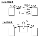
図3は、3軸加速度センサ16のデバイス上面から見た図である。図3に示されるように、ウエハ8に形成されるチップTPには、複数の電極パッドPDがその周辺に配置されている。そして、電気信号を電極パッドPDに対して伝達、あるいは電極パッドPDから伝達するために、金属配線が設けられている。そして、中央部には、クローバ型を形成する4つの重錘体ARが配置されている。
FIG. 3 is a view of the
図4は、3軸加速度センサ16の概略図である。図4に示す3軸加速度センサ16はピエゾ抵抗型であり、検出素子であるピエゾ抵抗素子が拡散抵抗として設けられている。このピエゾ抵抗型の加速度センサ16は、安価なICプロセスを利用して製造できる。検出素子である抵抗素子を小さく形成しても感度低下がないため、小型化・低コスト化に有利である。
FIG. 4 is a schematic diagram of the
具体的な構成としては、中央の重錘体ARは、4本のビームBMで支持された構造となっている。ビームBMはX、Yの2軸方向で互いに直交するように形成されており、1軸当たりに4つのピエゾ抵抗素子を備えている。Z軸方向検出用の4つのピエゾ抵抗素子は、X軸方向検出用ピエゾ抵抗素子の横に配置されている。重錘体ARの上面形状はクローバ型を形成し、中央部でビームBMと連結されている。このクローバ型構造を採用することにより、重錘体ARを大きくすると同時にビーム長を長くすることができるため、小型であっても高感度な加速度センサ16を実現することが可能である。
As a specific configuration, the center weight AR is supported by four beams BM. The beam BM is formed so as to be orthogonal to each other in the X-axis and Y-axis directions, and includes four piezoresistive elements per axis. Four piezoresistive elements for detecting the Z-axis direction are arranged beside the piezoresistive elements for detecting the X-axis direction. The top surface shape of the weight body AR forms a clover shape, and is connected to the beam BM at the center. By adopting this crowbar type structure, the weight AR can be enlarged and the beam length can be increased at the same time, so that it is possible to realize a highly
このピエゾ抵抗型の3軸加速度センサ16の動作原理は、重錘体ARが加速度(慣性力)を受けると、ビームBMが変形し、その表面に形成されたピエゾ抵抗素子の抵抗値の変化により加速度を検出するメカニズムである。そしてこのセンサ出力は、3軸それぞれに独立に組み込まれたホイートストンブリッジの出力から取り出す構成に設定されている。
The principle of operation of the piezoresistive
図5は、各軸方向の加速度を受けた場合の重錘体ARとビームBMの変形を説明する概念図である。図5に示されるようにピエゾ抵抗素子は、加えられたひずみによってその抵抗値が変化する性質(ピエゾ抵抗効果)を有しており、引っ張り歪みの場合は抵抗値が増加し、圧縮歪みの場合は抵抗値が減少する。本例においては、X軸方向用ピエゾ抵抗素子Rx1〜Rx4、Y軸方向検出用ピエゾ抵抗素子Ry1〜Ry4及びZ軸方向検出用ピエゾ抵抗素子Rz1〜Rz4が一例として示されている。 FIG. 5 is a conceptual diagram for explaining the deformation of the weight body AR and the beam BM when the acceleration in each axial direction is received. As shown in FIG. 5, the piezoresistive element has a property that its resistance value changes due to applied strain (piezoresistive effect). In the case of tensile strain, the resistance value increases, and in the case of compressive strain. The resistance value decreases. In this example, X-axis direction piezoresistive elements Rx1 to Rx4, Y-axis direction detecting piezoresistive elements Ry1 to Ry4, and Z-axis direction detecting piezoresistive elements Rz1 to Rz4 are shown as examples.
図6は、各軸に対して設けられるホイートストンブリッジの回路構成図である。図6(a)は、X(Y)軸におけるホイートストンブリッジの回路構成図である。X軸及びY軸の出力電圧としてはそれぞれVxout及びVyoutとする。図6(b)は、Z軸におけるホイートストンブリッジの回路構成図である。Z軸の出力電圧としてはVzoutとする。 FIG. 6 is a circuit configuration diagram of a Wheatstone bridge provided for each axis. FIG. 6A is a circuit configuration diagram of the Wheatstone bridge in the X (Y) axis. The output voltages of the X axis and Y axis are Vxout and Vyout, respectively. FIG. 6B is a circuit configuration diagram of the Wheatstone bridge in the Z-axis. The output voltage of the Z axis is Vzout.
上述したように、加えられた歪みによって各軸の4つのピエゾ抵抗素子の抵抗値は変化し、この変化に基づいて各ピエゾ抵抗素子は、例えばX軸Y軸においては、ホイートストンブリッジで形成される回路の出力各軸の加速度成分が独立に分離された出力電圧として検出される。なお、上記の回路が構成されるように図3で示されるような、金属配線等が連結され、所定の電極パッドPDから各軸に対する出力電圧が検出されるように構成されている。 As described above, the resistance values of the four piezoresistive elements on each axis change due to the applied strain. Based on this change, each piezoresistive element is formed by a Wheatstone bridge, for example, on the X axis and the Y axis. The acceleration component of each output axis of the circuit is detected as an independent output voltage. As shown in FIG. 3, metal wirings and the like are connected so that the above circuit is configured, and an output voltage for each axis is detected from a predetermined electrode pad PD.
再び図1及び図2を参照して、本発明の実施の形態における微小構造体の検査方法は、微小構造体である3軸加速度センサ16に対して、スピーカ10によってテスト音波を加えることにより、その音波に基づく微小構造体の可動部16aの動きを検出してその特性を評価する方式である。
Referring to FIGS. 1 and 2 again, in the microstructure inspection method in the embodiment of the present invention, a test sound wave is applied by the
次に、本発明の実施の形態における加速度センサ16の評価方法について説明する。
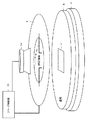
図7は、ウエハ8上の微小構造体を検査する概念構成図である。プローブカード4は、テスト音波出力部であるスピーカ10を備える。スピーカ10の音波が検査対象のチップTPに当たるように、プローブカード4には、テスト音波出力部の位置に開口領域が形成されている。プローブカード4には、プローブ4aが開口領域にせり出すように取り付けられている。また、開口領域の近くにマイクMが備えられる。マイクMによって、チップTPの近傍の音波を捉え、チップTPに印加される音波が所望の周波数成分になるように、スピーカ10から出力されるテスト音波を制御する。
Next, a method for evaluating the
FIG. 7 is a conceptual configuration diagram for inspecting a microstructure on the
スピーカ制御部3は、プローバ部15に与えられるテスト指示に応答してテスト音波を出力するものとする。これにより、例えば、3軸加速度センサ16の可動部16aが動くことになり、フリッティング現象により導通したプローブ4aを介して検査用電極から可動部16aの動きに応じた信号を検出することが可能である。この信号をプローブ制御部13で測定して解析することによりデバイス検査を実行することも可能である。
The
図8は、スピーカ10から出力されたテスト音波を調整しない場合のプローブカード4の構成を示す断面図である。ウエハ8の加速度センサ16は、理解を容易にするために1つだけ描かれている。実際にはウエハ8に加速度センサ16が複数個形成されている。図8では、可動部16aが上方に変位している様子を示す。
FIG. 8 is a cross-sectional view showing the configuration of the
ウエハ8は真空チャックのチャックトップ9に載置される。真空チャックはチャックトップ9の上面に真空溝91が形成されている。真空溝91はチャックトップ9の中を通る導通管で真空チャンバ(図示せず)に接続され、内部の気体が吸引される。真空溝91の負圧によって、ウエハ8はチャックトップ9に吸着される。
The
ウエハ8の加速度センサ16は、前述のとおり、重錘体ARの両側をビームBMで支持された両持ち梁構造の可動部16aを備える。BMにはピエゾ抵抗Rが形成されており、ビームBMの変形に伴う歪みを信号として出力する。加速度センサ16の電極にプローブ4aが接触し、ピエゾ抵抗Rの信号を外部に出力する。プローブカード4の上にスピーカ10が配置され、テスト音波を可動部16aに印加する。
As described above, the
スピーカ10から出力されたテスト音波は、プローブカード4の開口領域4bからプローブカード4とウエハ8の間に回り込み、反射されて可動部16aに戻る。また、テスト音波はプローブカード4の外側からプローブカード4とウエハ8の間に回り込み、可動部16aに達する。スピーカ10から出力されるテスト音波の直接波と、プローブカード4とウエハ8の間で反射されたテスト音波と、プローブカード4の外側から回り込んだテスト音波が可動部16aで干渉する。その結果、ある周波数では可動部16aの場所でテスト音波が弱まることになる。
The test sound wave output from the
なお、プローブカード4の外周に接続する筒状の部材を設けて、スピーカ10を覆い、プローブカード4の外側からプローブカード4とウエハ8の間にテスト音波が回り込むのを抑制する構造としてもよい。
In addition, it is good also as a structure which provides the cylindrical member connected to the outer periphery of the
スピーカ制御部3は可動部16aに所定の変動を加えるために、マイクMで可動部16aの近傍のテスト音波を検出し、テスト音波が所定の周波数と音圧になるようにスピーカ10の出力を制御する。反射波や回折波の干渉によってある周波数のテスト音波の音圧が弱くなると、スピーカ制御部3は所定の音圧になるようにスピーカ10への入力電圧を高くする。その結果、干渉による減衰が生じている周波数では、スピーカ10の入力電圧が高くなり、場合によっては過大な入力電圧になる。また過大な入力を原因とする高調波が発生することにもなる。入力電圧を大きくすると雑音成分も増加し、高調波歪みと共にS/N比を劣化させる。
The
図9は、本実施の形態1に係るプローブカード4の構成を示す断面図である。図9では、チャックトップ9を省略している。プローブカード4のウエハ8に対向する面に、吸音材11が形成されている。吸音材11は、弾力性があって内部損失の大きい材質、例えば、発泡した高分子材料で形成する。吸音材11は、広い周波数帯域で音波吸収率の高い材質、例えばスポンジ等が好ましい。
FIG. 9 is a cross-sectional view showing the configuration of the
次に、本発明の実施の形態1に従う微小構造体の検査方法について説明する。図20は本発明の実施の形態に係る検査装置1の動作の一例を示すフローチャートである。なお、検査制御部2の動作は、制御部21が主記憶部22、外部記憶部23、入力部24、入出力部25及び表示部26と協働して行う。
Next, a microstructure inspection method according to the first embodiment of the present invention will be described. FIG. 20 is a flowchart showing an example of the operation of the
検査制御部2はまず、ウエハ8がメインチャック14に載置され、測定開始が入力されるのを待機する(ステップS1)。測定開始指令が入力部24から入力されて制御部21に指示されると、制御部21は、プローブ制御部13にプローブ4aをウエハ8の電極パッドPDに位置合わせして接触するよう指令し(ステップS2)、ついで、プローブ制御部13にフリッティング用回路5によって、プローブ4aと電極パッドPDを導通させるように指令する(ステップS2)。
The inspection control unit 2 first waits for the
本実施の形態では、フリッティング現象を利用して電極パッドPDとプローブ4aの接触抵抗を低減させるが、接触抵抗を低減して導通させる方法としては、フリッティング技術以外の方法を利用してもよい。例えば、プローブ4aに超音波を伝導して、電極パッドPD表面の酸化膜を部分的に破って、電極パッドPDとプローブ4aの接触抵抗を低減させる方法を用いることができる。
In the present embodiment, the contact resistance between the electrode pad PD and the
ついで、測定方法の選択を入力する(ステップS3)。測定方法は、予め外部記憶部23に記憶されていてもよいし、測定の都度、入力部24から入力されてもよい。測定方法が入力されると、入力された測定方法によって用いる測定回路、及び可動部16aに印加するテスト音波の周波数と音圧などを設定する(ステップS4)。
Next, the selection of the measurement method is input (step S3). The measurement method may be stored in advance in the
選択される測定方法としては、例えば、テスト音波の周波数を順次変化させてそれぞれの周波数での応答を検査する周波数掃引検査(周波数スキャン)、所定の周波数範囲の擬似ホワイトノイズを印加して応答を検査するホワイトノイズ検査、周波数を所定の値に固定して音圧を変化させて応答を検査する直線性検査などがある。 As a measurement method to be selected, for example, a frequency sweep inspection (frequency scan) in which a response at each frequency is inspected by sequentially changing the frequency of the test sound wave, a pseudo white noise in a predetermined frequency range is applied, and a response is obtained. There are a white noise inspection for inspection, a linearity inspection for inspecting a response by changing the sound pressure while fixing the frequency to a predetermined value, and the like.
ついで、設定した測定方法でスピーカ制御部3を制御して、加速度センサ16の可動部16aを変位させながら、プローブ4aから加速度センサ16の応答である電気信号を検出し、加速度センサ16の応答特性を検査する(ステップS5)。そして、検出した測定結果を外部記憶部23に記憶すると同時に、表示部26に測定結果を表示する(ステップS6)。
Next, the
実施の形態1では、加速度センサ16の可動部16aに対してテスト音波を出力しながら、加速度センサ16を検査する。そのとき、プローブカード4とウエハ8の間に回り込んだテスト音波は、吸音材11によって吸収され、可動部16aへの反射波及び回折波が減衰される。したがって、可動部16aにおけるテスト音波の干渉が軽減される。その結果、干渉が発生していた周波数でのスピーカ10への入力電圧を下げることができる。同時に、高調波の発生を抑えることができる。入力電圧を下げるので雑音成分が減少し、高調波の抑制と合わせてS/N比が向上する。そして、特定の周波数領域でのテストデータの欠落が無くなりテストデータへの信頼性が高まる。また、スピーカ10に対する過大な電気入力が不要になり、検査装置1の寿命が延びる。
In the first embodiment, the
(実施例1)
図10は、スピーカ10から出力されたテスト音波を調整しない場合(すなわち図8)の、スピーカ10への入力電圧を示すグラフである。図11は、マイクMで検出したテスト音波の周波数成分を示すグラフである。図11に示すように、可動部16aの近傍におけるテスト音波の音圧が、検査する周波数に亘って一定になるように、スピーカ10の入力電圧を調節した結果が図10の入力電圧である。
Example 1
FIG. 10 is a graph showing the input voltage to the
図11に示すように、マイクMで検出したテスト音波の音圧が各周波数で110dBになるように、スピーカ10の入力電圧を調節した。図10の入力電圧Aに示すように、1580Hz付近と、3240Hz付近に著しいピークがある。それらの近くの周波数においてテスト音波が干渉によって減衰しているので、それを補うために入力電圧が高くなっている。
As shown in FIG. 11, the input voltage of the
図12は、図9に示す実施の形態1の構成におけるスピーカ10への入力電圧Bを示すグラフである。対比のために、出力されたテスト音波を調整しない場合のスピーカ10への入力電圧Aを合わせて記載している。この場合も、マイクMで検出したテスト音波の音圧が各周波数で110dBになるように、スピーカ10の入力電圧を調節した。
FIG. 12 is a graph showing the input voltage B to the
吸音材11によってプローブカード4とウエハ8の間の反射波及び回折波が減衰するので、可動部16aにおけるテスト音波の干渉が軽減され、入力電圧Bはピークが小さくなっている。特に3240Hz付近のピークは解消している。全体に入力電圧Bはほぼ0.9V以下であり、過大な入力電圧(例えば1.0V以上)の周波数がない。
Since the reflected wave and the diffracted wave between the
入力電圧Bの方が入力電圧Aより大きい周波数もあるが、その領域では干渉によってテスト音波が強められていると考えられる。しかし、その領域でも吸音材11がない場合(入力電圧A)は、干渉によってテスト音波波形の歪みや高調波の存在が推測される。
Although there are frequencies where the input voltage B is greater than the input voltage A, it is considered that the test sound wave is strengthened by interference in that region. However, when there is no
(実施の形態1の変形)
図13は、プローブカード4に音波の拡散部を設ける場合の断面図である。プローブカード4のウエハ8に対向する面に、音波を拡散させるように凹凸を有する拡散部17を形成する。プローブカード4のウエハ8に対向する面を凹凸形状に成形してもよいし、凹凸形状の部材を貼り付けて形成してもよい。拡散部17は音波をあらゆる方向に拡散させるように、不規則な凹凸形状とすることが望ましい。
(Modification of Embodiment 1)
FIG. 13 is a cross-sectional view when the
プローブカード4とウエハ8の間の反射波及び回折波は、拡散部17によって拡散して反射されるので、特定の場所、例えば可動部16aにおけるテスト音波の干渉が軽減される。その結果、吸音材11を形成する場合(図9)と類似の効果が得られる。吸音材11と拡散部17を組み合わせて、吸音材11の表面に凹凸を形成するとさらに効果がある。
Since the reflected wave and the diffracted wave between the
(実施の形態2)
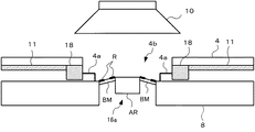
図14は、実施の形態2に係るプローブカード4の構成を示す断面図である。実施の形態2では、吸音材11に加えて、プローブカード4の開口領域周縁のウエハ8側にテスト音波の遮蔽部18を形成する。遮蔽部18は音波を通しにくい材質で、ある程度の硬さと質量及び幅を有するものが望ましい。
(Embodiment 2)
FIG. 14 is a cross-sectional view showing the configuration of the
遮蔽部18によって、テスト音波がプローブカード4の開口領域4bからプローブカード4とウエハ8の間へ回り込むのを抑制する。また、プローブカード4の外側からプローブカード4とウエハ8の間へ回り込んだテスト音波が、可動部16aに伝播するのを抑制する。
The shielding
遮蔽部18は、プローブ4aのポスト(固定台座)を兼ねている。遮蔽部18をプローブ4aのポストとすることによって、プローブカード4のウエハ8側に吸音材11を設けた場合でも、プローブ4aの支点をウエハ8の近くにすることができる。プローブ4aがコンプライアンスの高い(撓みやすい)材料で構成されても、ポスト部(遮蔽部18)は変形しにくい。ポスト部(遮蔽部18)によってプローブ4aのカンチレバー構造の支点が基板に近くなるので、プローブ4aの先端の変位方向がウエハ8にほぼ垂直になる。そのため、プローブカード4に対して基板面と垂直方向にウエハ8を移動してプローブ4aとウエハ8を接触させるようにすれば、プローブ4aの先端をウエハ8に接触させて、さらに所定の針圧になるようオーバードライブ量を変位させても、ウエハ8の表面に対して垂直方向の応力しか発生しない。その結果、微小構造体に対して基板面方向の応力がかからない状態で、微小構造体のテストを行うことができる。
The
吸音材11の効果に加えて、テスト音波の反射波と回折波が遮蔽部18によって抑制されるので、可動部16aにおけるテスト音波の干渉がさらに軽減される。その結果、干渉が発生していた周波数でのスピーカ10への入力電圧を下げることができる。同時に、高調波の発生を抑えることができる。入力電圧を下げるので雑音成分が減少し、高調波の抑制と合わせてS/N比が向上する。そして、特定の周波数領域でのテストデータの欠落が無くなりテストデータへの信頼性が高まる。また、スピーカ10に対する過大な電気入力が不要になり、検査装置1の寿命が延びる。
In addition to the effect of the
(実施例2)
図15は、図14に示す実施の形態2の構成におけるスピーカ10への入力電圧Cを示すグラフである。対比のために、実施の形態1の場合のスピーカ10への入力電圧Bを合わせて記載している。この場合も、マイクMで検出したテスト音波の音圧が各周波数で110dBになるように、スピーカ10の入力電圧を調節した。
(Example 2)
FIG. 15 is a graph showing the input voltage C to the
実施の形態1に比べて、遮蔽部18によって入力電圧が下がっている。特に、2000Hz以上の領域で、入力電圧Cは入力電圧Bより小さい。吸音材11で減衰しきれなかった反射波と回折波の周波数成分が、遮蔽部18によって抑制されたと考えられる。また、遮蔽部18によって、テスト音波が可動部16aに集中する度合いが大きくなったとも考えられる。
Compared to the first embodiment, the input voltage is lowered by the shielding
(実施の形態3)
図16は、実施の形態3に係るプローブカード4の構成を示す断面図である。実施の形態3では、吸音材11と遮蔽部18に加えて、スピーカ10とプローブカード4の間に、スピーカ10の開口周縁とプローブカード4の開口領域周縁を接続する面に沿って、ホーン19が形成されている。ホーン19は音波を通しにくい材質で、ある程度の硬さと質量及び幅を有するものが望ましい。また、スピーカ10の開口がプローブカード4の開口領域4bより大きい場合、スピーカ10の開口周縁とプローブカード4の開口領域周縁を接続する面に沿って、円錐台形にホーン19を形成するとよい。
(Embodiment 3)
FIG. 16 is a cross-sectional view showing the configuration of the
ホーン19によって、テスト音波がプローブカード4の開口領域4b以外に伝播することを抑制し、プローブカード4の開口領域4bを通じて可動部16aにテスト音波を集中させる。また、プローブカード4の外側からプローブカード4とウエハ8の間へテスト音波が回り込むのを抑制する。
The
ホーン19によってテスト音波が可動部16aに集中し、それ以外の領域に伝播するのを抑制するので、テスト音波の反射波と回折波が軽減し、可動部16aにおけるテスト音波の干渉がさらに軽減される。その結果、干渉が発生していた周波数でのスピーカ10への入力電圧を下げることができる。同時に、高調波の発生を抑えることができる。入力電圧を下げるので雑音成分が減少し、高調波の抑制と合わせてS/N比が向上する。そして、特定の周波数領域でのテストデータの欠落が無くなりテストデータへの信頼性が高まる。また、スピーカ10に対する過大な電気入力が不要になり、検査装置1の寿命が延びる。
The
(実施例3)
図17は、図16に示す実施の形態3の構成におけるスピーカ10への入力電圧Dを示すグラフである。対比のために、実施の形態2の場合のスピーカ10への入力電圧Cを合わせて記載している。この場合も、マイクMで検出したテスト音波の音圧が各周波数で110dBになるように、スピーカ10の入力電圧を調節した。
(Example 3)
FIG. 17 is a graph showing the input voltage D to the
実施の形態2に比べて、さらに殆どの周波数帯域で入力電圧が下がっている。特に、入力電圧Cでは1350Hz付近に0.85V程度のピークが残っていたのが、入力電圧Dでは0.3V以下に大幅に低下している。ホーン19によるテスト音波集中の効果が認められる。
Compared to the second embodiment, the input voltage is further reduced in most frequency bands. In particular, the peak of about 0.85 V remained in the vicinity of 1350 Hz at the input voltage C, but the input voltage D has greatly decreased to 0.3 V or less. The effect of test sound wave concentration by the
図18は、実施例1乃至3の結果をまとめて表したグラフである。出力されたテスト音波を調整しない場合の入力電圧Aと、プローブカード4に吸音材11を形成した場合の入力電圧Bと、吸音材11に加えて遮蔽部18を形成した場合の入力電圧Cと、吸音材11と遮蔽部18に加えてホーン19を形成した場合の入力電圧Dを1つのグラフにまとめて表している。いずれも、マイクMで検出したテスト音波の音圧が各周波数で110dBになるように、スピーカ10の入力電圧を調節した。
FIG. 18 is a graph summarizing the results of Examples 1 to 3. The input voltage A when the output test sound wave is not adjusted, the input voltage B when the
図18に示すように、入力電圧Aから入力電圧Dになるに従って、同じ音圧を得るためのスピーカ10への入力電圧が低下している。テスト音波の干渉を低減することについて、吸音材11、遮蔽部18、ホーン19それぞれの効果が認められる。特に、スピーカ入力のピーク電圧を下げる効果がある。
As shown in FIG. 18, as the input voltage A changes to the input voltage D, the input voltage to the
実施の形態では、加速度センサ16を例に説明したが、本発明の検査装置1はテスト音波で変動させることのできる可動部を有する微小構造体、例えば圧力センサなどの膜構造の可動部について適用することができる。図19は、圧力センサの例を説明する概念構成図である。図19(a)は圧力センサの平面図、図19(b)は図19(a)のA−A線断面図である。
In the embodiment, the
図19に示されるように、シリコン基板Siの中央部にほぼ正方形に、肉厚が薄い部分であるダイヤフラムDが形成されている。ダイヤフラムDの4辺の中央にそれぞれ、ピエゾ抵抗R1、R2、R3、R4が形成されている。ダイヤフラムDの両面にかかる圧力の差によって、ダイヤフラムDが変形すると、ピエゾ抵抗R1〜R4に応力が発生する。応力によって、ピエゾ抵抗R1〜R4の電気抵抗値が変化するので、その変化を検出することによって、ダイヤフラムDの両面にかかる圧力差を測ることができる。 As shown in FIG. 19, a diaphragm D, which is a thin portion, is formed in a substantially square shape at the center of the silicon substrate Si. Piezoresistors R1, R2, R3, and R4 are formed at the centers of the four sides of the diaphragm D, respectively. When the diaphragm D is deformed due to the difference in pressure applied to both surfaces of the diaphragm D, stress is generated in the piezoresistors R1 to R4. Since the electrical resistance values of the piezoresistors R1 to R4 change due to the stress, the pressure difference applied to both surfaces of the diaphragm D can be measured by detecting the change.
圧力センサについても、本発明の検査装置1によって、ダイヤフラムDに対してテスト音波を出力しながら変動を検出して特性を評価することができる。その場合、実施の形態1乃至3のプローブカード4を用いて、スピーカ10への入力電圧を下げることができる。同時に、高調波の発生を抑えることができる。そして、特定の周波数領域でのテストデータの欠落が無くなりテストデータへの信頼性が高まる。また、スピーカ10に対する過大な電気入力が不要になり、検査装置1の寿命が延びる。
With respect to the pressure sensor, the
その他、前記のハードウエア構成やフローチャートは一例であり、任意に変更及び修正が可能である。吸音材11、拡散部17、遮蔽部18及びホーン19は任意に組み合わせて用いることができる。
In addition, the hardware configuration and the flowchart described above are merely examples, and can be arbitrarily changed and modified. The
1 検査装置
2 検査制御部
3 スピーカ制御部
4 プローブカード
4a プローブ
4b 開口領域
6 特性評価部(評価手段)
7 切替部
8 ウエハ(基板)
10 スピーカ(音波発生手段)
11 吸音材(吸音手段)
13 プローブ制御部
15 プローバ部
16 加速度センサ(微小構造体)
16a 可動部
17 拡散部(音波拡散手段)
18 遮蔽部(遮蔽手段)
19 ホーン(音波集中手段)
AR 重錘体(可動部)
BM ビーム(可動部)
DESCRIPTION OF
7
10 Speaker (Sound wave generation means)
11 Sound absorbing material (sound absorbing means)
13
16a
18 Shielding part (shielding means)
19 Horn (Sound Concentration Means)
AR weight body (movable part)
BM beam (moving part)
Claims (5)
テスト時において前記基板上に形成された可動部の動きに基づく電気的変化量を検出するために、前記基板上に形成された前記微小構造体の検査用電極と電気的に接続されるプローブと、
前記プローブカードの前記基板に対向する面に設けられた、前記テスト音波を吸収する吸音手段を含む、前記テスト音波の反射又は干渉を抑制する音波調整手段と、
を備えることを特徴とするプローブカード。 A probe card connected to an evaluation means for outputting a test sound wave to the movable portion of the microstructure formed on the substrate and evaluating the characteristics of the microstructure,
A probe electrically connected to the inspection electrode of the microstructure formed on the substrate in order to detect an electrical change amount based on the movement of the movable part formed on the substrate during the test; ,
A sound wave adjusting means for suppressing reflection or interference of the test sound wave, including sound absorbing means for absorbing the test sound wave, provided on a surface of the probe card facing the substrate ;
A probe card comprising:
テスト時において前記基板上に形成された可動部の動きに基づく電気的変化量を検出するために、前記基板上に形成された前記微小構造体の検査用電極と電気的に接続されるプローブと、
前記プローブカードの前記基板に対向する面に設けられた、前記テスト音波を拡散する方向に反射させる音波拡散手段を含む、前記テスト音波の反射又は干渉を抑制する音波調整手段と、
を備えることを特徴とするプローブカード。 A probe card connected to an evaluation means for outputting a test sound wave to the movable portion of the microstructure formed on the substrate and evaluating the characteristics of the microstructure,
A probe electrically connected to the inspection electrode of the microstructure formed on the substrate in order to detect an electrical change amount based on the movement of the movable part formed on the substrate during the test; ,
Provided on opposite sides to the substrate before Symbol probe card, including a sound wave spreading means for reflecting in the direction of spreading the test sound wave, and suppresses waves adjusting means reflections or interference of the test sound wave,
Features and to pulp lobes cards in that it comprises.
テスト時において前記基板上に形成された可動部の動きに基づく電気的変化量を検出するために、前記基板上に形成された前記微小構造体の検査用電極と電気的に接続されるプローブと、
前記プローブカードと前記基板との間に、前記テスト音波を前記微小構造体の近傍領域から外部に伝播することを抑制する遮蔽手段を含む、前記テスト音波の反射又は干渉を抑制する音波調整手段と、
を備えることを特徴とするプローブカード。 A probe card connected to an evaluation means for outputting a test sound wave to the movable portion of the microstructure formed on the substrate and evaluating the characteristics of the microstructure,
A probe electrically connected to the inspection electrode of the microstructure formed on the substrate in order to detect an electrical change amount based on the movement of the movable part formed on the substrate during the test; ,
Between the front Symbol probe card and the substrate, including suppressing shielding means to propagate the test sound wave to the outside from the vicinity region of the micro structure, suppresses reflection or interference of the test sound wave sound wave adjusting means When,
Features and to pulp lobes cards in that it comprises.
前記微小構造体の可動部に対してテスト音波を出力する音波発生手段と、
請求項1乃至4のいずれか1項に記載のプローブカードと、
前記プローブカードと接続され、前記微小構造体の特性を評価するための評価手段とを備え、
前記評価手段は、前記プローブを介して前記音波発生手段により出力された前記テスト音波に応答した前記微小構造体の可動部の動きを検出し、その検出結果に基づいて前記微小構造体の特性を評価する、
ことを特徴とする微小構造体の検査装置。 A microstructure inspection apparatus comprising an evaluation means for evaluating the characteristics of at least one microstructure having a movable part formed on a substrate,
Sound wave generating means for outputting a test sound wave to the movable portion of the microstructure,
A probe card according to any one of claims 1 to 4,
An evaluation means connected to the probe card for evaluating the characteristics of the microstructure,
The evaluation means detects the movement of the movable portion of the microstructure in response to the test sound wave output by the sound wave generation means via the probe, and determines the characteristics of the microstructure based on the detection result. evaluate,
A microstructure inspection apparatus characterized by the above.
Priority Applications (5)
| Application Number | Priority Date | Filing Date | Title |
|---|---|---|---|
| JP2006268431A JP5121202B2 (en) | 2006-09-29 | 2006-09-29 | Probe card and microstructure inspection device |
| US12/294,481 US20100225342A1 (en) | 2006-09-29 | 2007-09-28 | Probe card and microstructure inspecting apparatus |
| KR1020087020894A KR101013594B1 (en) | 2006-09-29 | 2007-09-28 | Probe card and microstructure inspecting apparatus |
| PCT/JP2007/069003 WO2008038781A1 (en) | 2006-09-29 | 2007-09-28 | Probe card and inspection device of minute structure |
| TW096136673A TW200831902A (en) | 2006-09-29 | 2007-09-29 | Probe card and inspection device of minute structure |
Applications Claiming Priority (1)
| Application Number | Priority Date | Filing Date | Title |
|---|---|---|---|
| JP2006268431A JP5121202B2 (en) | 2006-09-29 | 2006-09-29 | Probe card and microstructure inspection device |
Publications (2)
| Publication Number | Publication Date |
|---|---|
| JP2008089350A JP2008089350A (en) | 2008-04-17 |
| JP5121202B2 true JP5121202B2 (en) | 2013-01-16 |
Family
ID=39230213
Family Applications (1)
| Application Number | Title | Priority Date | Filing Date |
|---|---|---|---|
| JP2006268431A Expired - Fee Related JP5121202B2 (en) | 2006-09-29 | 2006-09-29 | Probe card and microstructure inspection device |
Country Status (5)
| Country | Link |
|---|---|
| US (1) | US20100225342A1 (en) |
| JP (1) | JP5121202B2 (en) |
| KR (1) | KR101013594B1 (en) |
| TW (1) | TW200831902A (en) |
| WO (1) | WO2008038781A1 (en) |
Families Citing this family (2)
| Publication number | Priority date | Publication date | Assignee | Title |
|---|---|---|---|---|
| WO2017014060A1 (en) * | 2015-07-23 | 2017-01-26 | 株式会社東京精密 | Prober and probe contact method |
| SE2251043A1 (en) * | 2022-09-08 | 2024-03-09 | Silex Microsystems Ab | Microstructure inspection device and system and use of the same |
Family Cites Families (10)
| Publication number | Priority date | Publication date | Assignee | Title |
|---|---|---|---|---|
| JPS63157029A (en) * | 1986-12-22 | 1988-06-30 | Agency Of Ind Science & Technol | Measuring method for dynamic response characteristic or strain gauge |
| JP2811003B2 (en) * | 1989-02-28 | 1998-10-15 | 昭和電線電纜株式会社 | Partial discharge detection device |
| JPH04198736A (en) * | 1990-11-29 | 1992-07-20 | Nichiei Denshi Kogyo Kk | Detecting method for structure defect and detecting device thereof |
| JPH0534371A (en) * | 1991-07-31 | 1993-02-09 | Tokai Rika Co Ltd | Measuring apparatus for sensitivity of semiconductor acceleration sensor |
| JPH0933567A (en) * | 1995-07-21 | 1997-02-07 | Akebono Brake Ind Co Ltd | Method and device for inspecting sensor chip of semiconductor acceleration sensor |
| US6232790B1 (en) * | 1999-03-08 | 2001-05-15 | Honeywell Inc. | Method and apparatus for amplifying electrical test signals from a micromechanical device |
| JP2001264185A (en) * | 2000-03-21 | 2001-09-26 | Nikon Corp | Method and instrument for measuring internal stress of membrane of reticle and method for manufacturing semiconductor device |
| FR2847384B1 (en) * | 2002-11-01 | 2008-08-29 | Suss Microtec Test Systems Gmbh | METHOD AND DEVICE FOR TESTING MOTION SENSITIVE SUBSTRATES |
| WO2006093232A1 (en) * | 2005-03-03 | 2006-09-08 | Tokyo Electron Limited | Minute structure inspection device, minute structure inspection method, and minute structure inspection program |
| JP4573794B2 (en) * | 2005-03-31 | 2010-11-04 | 東京エレクトロン株式会社 | Probe card and microstructure inspection device |
-
2006
- 2006-09-29 JP JP2006268431A patent/JP5121202B2/en not_active Expired - Fee Related
-
2007
- 2007-09-28 US US12/294,481 patent/US20100225342A1/en not_active Abandoned
- 2007-09-28 KR KR1020087020894A patent/KR101013594B1/en not_active IP Right Cessation
- 2007-09-28 WO PCT/JP2007/069003 patent/WO2008038781A1/en active Application Filing
- 2007-09-29 TW TW096136673A patent/TW200831902A/en not_active IP Right Cessation
Also Published As
| Publication number | Publication date |
|---|---|
| TWI338138B (en) | 2011-03-01 |
| KR101013594B1 (en) | 2011-02-14 |
| WO2008038781A1 (en) | 2008-04-03 |
| US20100225342A1 (en) | 2010-09-09 |
| TW200831902A (en) | 2008-08-01 |
| JP2008089350A (en) | 2008-04-17 |
| KR20080106206A (en) | 2008-12-04 |
Similar Documents
| Publication | Publication Date | Title |
|---|---|---|
| JPWO2008053929A1 (en) | Micro structure inspection apparatus, micro structure inspection method, and substrate holding apparatus | |
| US20090128171A1 (en) | Microstructure Probe Card, and Microstructure Inspecting Device, Method, and Computer Program | |
| JP4573794B2 (en) | Probe card and microstructure inspection device | |
| US20080302185A1 (en) | Microstructure Inspecting Apparatus and Microstructure Inspecting Method | |
| JP2006313137A (en) | Inspection device of micro structure, inspection method of micro structure and inspection program of microstructure | |
| KR101019080B1 (en) | Microstructure inspecting apparatus and microstructure inspecting method | |
| JP5121202B2 (en) | Probe card and microstructure inspection device | |
| EP1930732A1 (en) | Minute structure inspection device, inspection method, and inspection program | |
| US20080223136A1 (en) | Minute structure inspection device, inspection method, and inspection program | |
| JP4856426B2 (en) | Micro structure inspection apparatus and micro structure inspection method | |
| JP2010048597A (en) | Apparatus and method for inspecting minute structure | |
| WO2007018186A1 (en) | Apparatus and method for inspecting fine structure and inspection program | |
| JP4822846B2 (en) | Microstructure inspection apparatus, microstructure inspection method, and microstructure inspection program |
Legal Events
| Date | Code | Title | Description |
|---|---|---|---|
| A621 | Written request for application examination |
Free format text: JAPANESE INTERMEDIATE CODE: A621 Effective date: 20090701 |
|
| A131 | Notification of reasons for refusal |
Free format text: JAPANESE INTERMEDIATE CODE: A131 Effective date: 20120124 |
|
| A521 | Written amendment |
Free format text: JAPANESE INTERMEDIATE CODE: A523 Effective date: 20120308 |
|
| TRDD | Decision of grant or rejection written | ||
| A01 | Written decision to grant a patent or to grant a registration (utility model) |
Free format text: JAPANESE INTERMEDIATE CODE: A01 Effective date: 20121023 |
|
| A01 | Written decision to grant a patent or to grant a registration (utility model) |
Free format text: JAPANESE INTERMEDIATE CODE: A01 |
|
| A61 | First payment of annual fees (during grant procedure) |
Free format text: JAPANESE INTERMEDIATE CODE: A61 Effective date: 20121023 |
|
| FPAY | Renewal fee payment (event date is renewal date of database) |
Free format text: PAYMENT UNTIL: 20151102 Year of fee payment: 3 |
|
| R150 | Certificate of patent or registration of utility model |
Free format text: JAPANESE INTERMEDIATE CODE: R150 |
|
| LAPS | Cancellation because of no payment of annual fees |