JP5118939B2 - Liquid crystal drive device and liquid crystal display device using the same - Google Patents
Liquid crystal drive device and liquid crystal display device using the same Download PDFInfo
- Publication number
- JP5118939B2 JP5118939B2 JP2007277160A JP2007277160A JP5118939B2 JP 5118939 B2 JP5118939 B2 JP 5118939B2 JP 2007277160 A JP2007277160 A JP 2007277160A JP 2007277160 A JP2007277160 A JP 2007277160A JP 5118939 B2 JP5118939 B2 JP 5118939B2
- Authority
- JP
- Japan
- Prior art keywords
- power supply
- liquid crystal
- supply voltage
- effect transistor
- field effect
- Prior art date
- Legal status (The legal status is an assumption and is not a legal conclusion. Google has not performed a legal analysis and makes no representation as to the accuracy of the status listed.)
- Expired - Fee Related
Links
- 239000004973 liquid crystal related substance Substances 0.000 title claims description 86
- 210000002858 crystal cell Anatomy 0.000 claims description 26
- 230000005669 field effect Effects 0.000 claims description 20
- 238000012544 monitoring process Methods 0.000 claims description 19
- 230000004044 response Effects 0.000 claims description 7
- 230000007704 transition Effects 0.000 claims description 2
- 238000000034 method Methods 0.000 description 8
- 238000010586 diagram Methods 0.000 description 7
- 230000007274 generation of a signal involved in cell-cell signaling Effects 0.000 description 7
- 230000007423 decrease Effects 0.000 description 3
- 239000003990 capacitor Substances 0.000 description 2
- 238000007599 discharging Methods 0.000 description 2
- 230000006870 function Effects 0.000 description 2
- 238000009499 grossing Methods 0.000 description 2
- 239000011159 matrix material Substances 0.000 description 2
- 230000005540 biological transmission Effects 0.000 description 1
- 239000004065 semiconductor Substances 0.000 description 1
Images


Classifications
-
- G—PHYSICS
- G09—EDUCATION; CRYPTOGRAPHY; DISPLAY; ADVERTISING; SEALS
- G09G—ARRANGEMENTS OR CIRCUITS FOR CONTROL OF INDICATING DEVICES USING STATIC MEANS TO PRESENT VARIABLE INFORMATION
- G09G3/00—Control arrangements or circuits, of interest only in connection with visual indicators other than cathode-ray tubes
- G09G3/20—Control arrangements or circuits, of interest only in connection with visual indicators other than cathode-ray tubes for presentation of an assembly of a number of characters, e.g. a page, by composing the assembly by combination of individual elements arranged in a matrix no fixed position being assigned to or needed to be assigned to the individual characters or partial characters
- G09G3/34—Control arrangements or circuits, of interest only in connection with visual indicators other than cathode-ray tubes for presentation of an assembly of a number of characters, e.g. a page, by composing the assembly by combination of individual elements arranged in a matrix no fixed position being assigned to or needed to be assigned to the individual characters or partial characters by control of light from an independent source
- G09G3/36—Control arrangements or circuits, of interest only in connection with visual indicators other than cathode-ray tubes for presentation of an assembly of a number of characters, e.g. a page, by composing the assembly by combination of individual elements arranged in a matrix no fixed position being assigned to or needed to be assigned to the individual characters or partial characters by control of light from an independent source using liquid crystals
- G09G3/3611—Control of matrices with row and column drivers
-
- G—PHYSICS
- G09—EDUCATION; CRYPTOGRAPHY; DISPLAY; ADVERTISING; SEALS
- G09G—ARRANGEMENTS OR CIRCUITS FOR CONTROL OF INDICATING DEVICES USING STATIC MEANS TO PRESENT VARIABLE INFORMATION
- G09G2310/00—Command of the display device
- G09G2310/02—Addressing, scanning or driving the display screen or processing steps related thereto
- G09G2310/0243—Details of the generation of driving signals
- G09G2310/0245—Clearing or presetting the whole screen independently of waveforms, e.g. on power-on
-
- G—PHYSICS
- G09—EDUCATION; CRYPTOGRAPHY; DISPLAY; ADVERTISING; SEALS
- G09G—ARRANGEMENTS OR CIRCUITS FOR CONTROL OF INDICATING DEVICES USING STATIC MEANS TO PRESENT VARIABLE INFORMATION
- G09G2310/00—Command of the display device
- G09G2310/02—Addressing, scanning or driving the display screen or processing steps related thereto
- G09G2310/0264—Details of driving circuits
- G09G2310/0278—Details of driving circuits arranged to drive both scan and data electrodes
-
- G—PHYSICS
- G09—EDUCATION; CRYPTOGRAPHY; DISPLAY; ADVERTISING; SEALS
- G09G—ARRANGEMENTS OR CIRCUITS FOR CONTROL OF INDICATING DEVICES USING STATIC MEANS TO PRESENT VARIABLE INFORMATION
- G09G2320/00—Control of display operating conditions
- G09G2320/02—Improving the quality of display appearance
- G09G2320/0257—Reduction of after-image effects
-
- G—PHYSICS
- G09—EDUCATION; CRYPTOGRAPHY; DISPLAY; ADVERTISING; SEALS
- G09G—ARRANGEMENTS OR CIRCUITS FOR CONTROL OF INDICATING DEVICES USING STATIC MEANS TO PRESENT VARIABLE INFORMATION
- G09G2330/00—Aspects of power supply; Aspects of display protection and defect management
- G09G2330/02—Details of power systems and of start or stop of display operation
- G09G2330/027—Arrangements or methods related to powering off a display
-
- G—PHYSICS
- G09—EDUCATION; CRYPTOGRAPHY; DISPLAY; ADVERTISING; SEALS
- G09G—ARRANGEMENTS OR CIRCUITS FOR CONTROL OF INDICATING DEVICES USING STATIC MEANS TO PRESENT VARIABLE INFORMATION
- G09G2330/00—Aspects of power supply; Aspects of display protection and defect management
- G09G2330/12—Test circuits or failure detection circuits included in a display system, as permanent part thereof
-
- G—PHYSICS
- G09—EDUCATION; CRYPTOGRAPHY; DISPLAY; ADVERTISING; SEALS
- G09G—ARRANGEMENTS OR CIRCUITS FOR CONTROL OF INDICATING DEVICES USING STATIC MEANS TO PRESENT VARIABLE INFORMATION
- G09G3/00—Control arrangements or circuits, of interest only in connection with visual indicators other than cathode-ray tubes
- G09G3/20—Control arrangements or circuits, of interest only in connection with visual indicators other than cathode-ray tubes for presentation of an assembly of a number of characters, e.g. a page, by composing the assembly by combination of individual elements arranged in a matrix no fixed position being assigned to or needed to be assigned to the individual characters or partial characters
- G09G3/34—Control arrangements or circuits, of interest only in connection with visual indicators other than cathode-ray tubes for presentation of an assembly of a number of characters, e.g. a page, by composing the assembly by combination of individual elements arranged in a matrix no fixed position being assigned to or needed to be assigned to the individual characters or partial characters by control of light from an independent source
- G09G3/36—Control arrangements or circuits, of interest only in connection with visual indicators other than cathode-ray tubes for presentation of an assembly of a number of characters, e.g. a page, by composing the assembly by combination of individual elements arranged in a matrix no fixed position being assigned to or needed to be assigned to the individual characters or partial characters by control of light from an independent source using liquid crystals
- G09G3/3611—Control of matrices with row and column drivers
- G09G3/3622—Control of matrices with row and column drivers using a passive matrix
-
- G—PHYSICS
- G09—EDUCATION; CRYPTOGRAPHY; DISPLAY; ADVERTISING; SEALS
- G09G—ARRANGEMENTS OR CIRCUITS FOR CONTROL OF INDICATING DEVICES USING STATIC MEANS TO PRESENT VARIABLE INFORMATION
- G09G3/00—Control arrangements or circuits, of interest only in connection with visual indicators other than cathode-ray tubes
- G09G3/20—Control arrangements or circuits, of interest only in connection with visual indicators other than cathode-ray tubes for presentation of an assembly of a number of characters, e.g. a page, by composing the assembly by combination of individual elements arranged in a matrix no fixed position being assigned to or needed to be assigned to the individual characters or partial characters
- G09G3/34—Control arrangements or circuits, of interest only in connection with visual indicators other than cathode-ray tubes for presentation of an assembly of a number of characters, e.g. a page, by composing the assembly by combination of individual elements arranged in a matrix no fixed position being assigned to or needed to be assigned to the individual characters or partial characters by control of light from an independent source
- G09G3/36—Control arrangements or circuits, of interest only in connection with visual indicators other than cathode-ray tubes for presentation of an assembly of a number of characters, e.g. a page, by composing the assembly by combination of individual elements arranged in a matrix no fixed position being assigned to or needed to be assigned to the individual characters or partial characters by control of light from an independent source using liquid crystals
- G09G3/3611—Control of matrices with row and column drivers
- G09G3/3696—Generation of voltages supplied to electrode drivers
Landscapes
- Engineering & Computer Science (AREA)
- Chemical & Material Sciences (AREA)
- Crystallography & Structural Chemistry (AREA)
- Physics & Mathematics (AREA)
- Computer Hardware Design (AREA)
- General Physics & Mathematics (AREA)
- Theoretical Computer Science (AREA)
- Control Of Indicators Other Than Cathode Ray Tubes (AREA)
- Liquid Crystal Display Device Control (AREA)
- Liquid Crystal (AREA)
Description
本発明は、液晶セルの駆動制御を行う液晶駆動装置、及び、これを用いた液晶表示装置に関するものである。 The present invention relates to a liquid crystal driving device that controls driving of a liquid crystal cell, and a liquid crystal display device using the same.
近年、パーソナルコンピュータや携帯電話端末の表示手段として、液晶表示装置が広く一般に用いられている。 In recent years, liquid crystal display devices have been widely used as display means for personal computers and mobile phone terminals.
なお、液晶表示装置やその電源装置に関連する従来技術の一例としては、下記の特許文献1、2を挙げることができる。
ところで、液晶表示装置のドライバICには、図4に示すように、ロジック回路系(ロジック部100)を駆動するための第1電源電圧Vcc1(例えば1.8[V])と、アナログ回路系(リセット信号生成部200やドライバ部300など)を駆動するための第2電源電圧Vcc2(例えば2.8[V])が供給されており、液晶表示装置の電源オフ時には、リセット信号生成部200から出力されるリセット信号ENをトリガとして、ドライバ部300による液晶セルの放電処理が行われていた。このようなシーケンスによれば、液晶セルに蓄積された電荷を放電した後に、液晶表示装置の動作を停止することができるので、液晶表示パネルに意図しないライン表示を生じることはない。
Incidentally, as shown in FIG. 4, the driver IC of the liquid crystal display device includes a first power supply voltage Vcc1 (for example, 1.8 [V]) for driving the logic circuit system (logic unit 100), and an analog circuit system. A second power supply voltage Vcc2 (for example, 2.8 [V]) for driving (reset
しかしながら、液晶表示装置の動作中に電池が取り外された場合など、通常とは異なるシーケンスで電源がオフされた場合、従来のドライバICでは、リセット信号生成部200からドライバ部300に対してリセット信号ENを送出する前に、アナログ回路系を駆動するための第2電源電圧Vcc2がアナログ回路系の最低動作保証電圧(アナログ回路系の正常動作を保証することができる最低電圧)を下回ってしまい、リセット信号生成部200が動作不能となるおそれがあった。このような状態に陥ってしまうと、従来のドライバICでは、ドライバ部300による液晶セルの放電処理を実施することができないため、液晶表示装置の動作が停止された後も、液晶セルに意図しない電荷が残留したままとなり、これが液晶表示パネルに意図しないライン表示を生じる原因となっていた。
However, when the power is turned off in an unusual sequence, such as when the battery is removed during the operation of the liquid crystal display device, the conventional driver IC uses a reset signal from the reset
本発明は、上記問題点に鑑み、電源オフに際して確実に液晶セルの電荷を放電することが可能な液晶駆動装置、及び、これを用いた液晶表示装置を提供することを目的とする。 In view of the above problems, an object of the present invention is to provide a liquid crystal driving device capable of reliably discharging a charge of a liquid crystal cell when the power is turned off, and a liquid crystal display device using the same.
上記の目的を達成するために、本発明に係る液晶駆動装置は、第1電源電圧を駆動電圧とし、第1電源電圧よりも高い第2電源電圧を監視して、これが所定の閾値を下回っているか否かを示すモニタ信号を生成する電源監視部と;第1電源電圧を駆動電圧とし、前記モニタ信号に応じてリセットリクエスト信号を生成するロジック部と;第2電源電圧を駆動電圧とし、前記リセットリクエスト信号に応じてリセット信号を生成するリセット信号生成部と;第2電源電圧を駆動電圧とし、前記リセット信号に応じて液晶セルの放電処理を行うドライバ部と;を有して成る構成(第1の構成)とされている。 In order to achieve the above object, a liquid crystal driving device according to the present invention uses a first power supply voltage as a drive voltage, monitors a second power supply voltage higher than the first power supply voltage, and falls below a predetermined threshold. A power supply monitoring unit for generating a monitor signal indicating whether or not; a logic unit for generating a reset request signal in response to the first power supply voltage as a drive voltage; and a second power supply voltage as a drive voltage; A configuration including: a reset signal generating unit that generates a reset signal in response to a reset request signal; and a driver unit that uses the second power supply voltage as a driving voltage and discharges the liquid crystal cell in response to the reset signal. First configuration).
なお、上記第1の構成から成る液晶駆動装置において、前記電源監視部は、アノードが第2電源電圧の印加端に接続されたダイオードと、ソースが第1電源電圧の印加端に接続され、ゲートが前記ダイオードのカソードに接続されたPチャネル型電界効果トランジスタと、を有して成り、前記Pチャネル型電界効果トランジスタのドレイン電圧に応じて前記モニタ信号の論理変遷を行う構成(第2の構成)にするとよい。 In the liquid crystal driving device having the first configuration, the power monitoring unit includes a diode having an anode connected to the application terminal for the second power supply voltage, a source connected to the application terminal for the first power supply voltage, and a gate. And a P-channel field effect transistor connected to the cathode of the diode, and a logic transition of the monitor signal according to the drain voltage of the P-channel field effect transistor (second configuration) ).
また、上記第1または第2の構成から成る液晶駆動装置は、前記モニタ信号と外部リセット信号との論理演算信号を生成する論理ゲート部を有して成り、前記ロジック部は、前記論理演算信号に応じて前記リセットリクエスト信号を生成する構成(第3の構成)にするとよい。 The liquid crystal driving device having the first or second configuration includes a logic gate unit that generates a logic operation signal of the monitor signal and the external reset signal, and the logic unit includes the logic operation signal. The reset request signal may be generated according to the configuration (third configuration).
また、本発明に係る液晶表示装置は、複数の走査線と複数の信号線との間に液晶セルを挟持して成る液晶表示パネルと、前記液晶セルの駆動制御を行う上記第1〜第3いずれかの構成から成る液晶駆動装置と、を有して成る構成(第4の構成)とされている。 The liquid crystal display device according to the present invention includes a liquid crystal display panel in which a liquid crystal cell is sandwiched between a plurality of scanning lines and a plurality of signal lines, and the first to third embodiments that control driving of the liquid crystal cell. A liquid crystal driving device having any one of the configurations is provided (fourth configuration).
本発明によれば、電源オフに際して確実に液晶セルの電荷を放電することができる。 According to the present invention, it is possible to reliably discharge the liquid crystal cell when the power is turned off.
以下では、本発明を液晶表示装置に適用した場合を例に挙げて、詳細な説明を行う。 Hereinafter, the case where the present invention is applied to a liquid crystal display device will be described in detail as an example.
図1は、本発明に係る液晶表示装置の一実施形態を示す図である。 FIG. 1 is a diagram showing an embodiment of a liquid crystal display device according to the present invention.
図1に示すように、本実施形態の液晶表示装置は、液晶駆動装置1と、その駆動対象である液晶表示パネル2と、を有して成る。
As shown in FIG. 1, the liquid crystal display device of the present embodiment includes a liquid
液晶駆動装置1は、液晶表示パネル2の液晶セルを駆動する容量負荷駆動装置であり、ロジック部11と、メモリ部12と、セグメントドライバ部13と、コモンドライバ部14と、電源部15と、を集積化して成る半導体装置である。
The liquid
ロジック部11は、映像信号や制御信号の入力を受け、液晶表示の制御に必要な各種信号(データ信号やコモン選択信号等を含む)をセグメントドライバ部13及びコモンドライバ部14に供給する手段であり、データレジスタ、コマンドデコーダ、MPU[Micro Processing Unit]インターフェイス、コントロールレジスタ、アドレスカウンタ、タイミングジェネレータなどを有して成る(いずれも不図示)。
The
メモリ部12は、ロジック部11で生成されたセグメント制御信号を一旦格納し、これを適宜読み出してセグメントドライバ部13に送出するバッファ手段である。
The
セグメントドライバ部13は、ロジック部11から入力されるデータ信号(延いては、装置外部から入力される映像信号)に応じてセグメント駆動信号X1〜Xmを生成し、これらを液晶表示パネル1の各信号線(液晶セルの各一端)に供給する手段である。
The
コモンドライバ部14は、ロジック部11から入力されるコモン選択信号に応じてコモン駆動信号Y1〜Ynを生成し、これらを液晶表示パネル1の各走査線(液晶セルの各他端)に供給する手段である。
The
電源部15は、装置外部から第1電源電圧Vcc1(主としてロジック回路系を駆動するための電源電圧であり、例えば1.8[V])と、第2電源電圧Vcc2(主としてアナログ回路系を駆動するための電源電圧であり、例えば2.8[V])の入力を受けて、ロジック部11、メモリ部12、セグメントドライバ部13、及び、コモンドライバ部14にそれぞれ電力供給を行う手段である。なお、電源部15には、第1電源電圧Vcc1や第2電源電圧Vcc2の供給ラインに平滑キャパシタが接続されており、液晶表示装置の電源オフ時において、第1電源電圧Vcc1及び第2電源電圧Vcc2は、上記した平滑キャパシタの放電に伴って、その電圧レベルが徐々に低下していく。
The
液晶表示パネル2は、複数の信号線(セグメント信号線)とこれに直交する複数の走査線(コモン信号線)との各交点にそれぞれ液晶セルを挟持して成る単純マトリクス型(STN[Super Twisted Nematic]型)の液晶表示パネルであり、各液晶セルの両端間に電圧をかけることで液晶分子の向きを変え、光の透過を制御することによって、任意の文字や画像を表示するものである。
The liquid
次に、液晶表示装置の電源オフ時における液晶セルの放電処理について説明する。 Next, the discharge process of the liquid crystal cell when the power of the liquid crystal display device is turned off will be described.
図2は、液晶セルの放電処理を実現するためのブロック図である。 FIG. 2 is a block diagram for realizing the discharge process of the liquid crystal cell.
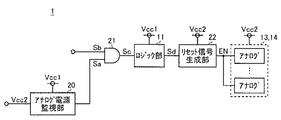
図2に示すように、本実施形態の液晶駆動装置1は、液晶セルの放電処理に関連する回路ブロックとして、先出の図1で示した回路ブロック11〜15のほかに、アナログ電源監視部20と、論理積演算器21と、リセット信号生成部22と、を有して成る。
As shown in FIG. 2, the liquid
アナログ電源監視部20は、第1電源電圧Vcc1を駆動電圧とし、第1電源電圧Vcc1よりも高い第2電源電圧Vcc2を監視して、これが所定の閾値(アナログ回路系の最低動作保証電圧よりも高い任意の電圧値)を下回っているか否かを示すモニタ信号Saを生成する手段である。なお、モニタ信号Saは、例えば、第2電源電圧Vcc2が所定の閾値を下回っていればローレベルとなり、下回っていなければハイレベルとなる2値信号である。アナログ電源監視部20の内部構成及び動作については、後ほど詳述する。
The analog power
論理積演算器21は、モニタ信号Saと外部リセット信号Sbとの論理積演算信号Scを生成する論理ゲート部である。すなわち、論理積演算信号Scは、モニタ信号Saと外部リセット信号Sbが共にハイレベルである場合にのみハイレベルとなり、その余の場合にはローレベルとなる2値信号である。
The
ロジック部11は、第1電源電圧Vcc1を駆動電圧とし、先述した諸機能を実現するほか、論理積演算信号Scに応じてリセットリクエスト信号Sdを生成する手段である。なお、ロジック部11は、論理積演算信号Scの立下がりエッジをトリガとして、リセットリクエスト信号Sdの送出を行う。
The
リセット信号生成部22は、第2電源電圧Vcc2を駆動電圧とし、リセットリクエスト信号Sdに応じてリセット信号ENを生成する手段である。
The reset
セグメントドライバ部13及びコモンドライバ部14は、第2電源電圧Vcc2を駆動電圧とし、先述した諸機能を実現するほか、リセット信号ENに応じて液晶セル(図2では不図示)の放電処理を行う手段である。
The
上記構成から成る液晶駆動装置1において、ロジック部11は、外部リセット信号Sbがローレベルとされた場合だけでなく、アナログ電源監視部20にて第2電源電圧Vcc2が所定の閾値を下回ったことが検出され、モニタ信号Saがローレベルとされた場合にも、リセット信号生成部22に対してリセットリクエスト信号Sdを送出する。
In the liquid
従って、液晶表示装置の動作中に電池が取り外された場合など、通常とは異なるシーケンスで電源がオフされたとしても、第2電源電圧Vcc2がアナログ回路系の最低動作保証電圧を下回る前に、リセット信号生成部22からセグメントドライバ部13及びコモンドライバ部14に対してリセット信号ENを送出し、液晶セルに蓄積された電荷を確実に放電した後に、液晶表示装置の動作を停止することが可能となるので、液晶表示パネル2に意図しないライン表示を生じるおそれがなくなる。
Therefore, even when the power is turned off in an unusual sequence, such as when the battery is removed during operation of the liquid crystal display device, before the second power supply voltage Vcc2 falls below the minimum guaranteed operation voltage of the analog circuit system, It is possible to stop the operation of the liquid crystal display device after the reset signal EN 22 sends a reset signal EN to the
なお、液晶表示装置の電源オフに伴い、第2電源電圧Vcc2だけでなく、第1電源電圧Vcc1も当然に低下するが、第2電源電圧Vcc2がアナログ回路系の最低動作保証電圧を下回る前であれば、第1電源電圧Vcc1もロジック回路系の最低動作保証電圧を下回ることはないと考えられるので、上記のリセット動作に支障が生じることはない。また、第1電源電圧Vcc1が第2電源電圧Vcc2よりも先に低下した場合でも、第2電源電圧Vcc2が最低動作保証電圧を下回らない領域では、ロジック部11からのリセットリクエスト信号Sdがローレベルとなってリセットがかかるため、回路に問題が生じることはない。
As the liquid crystal display device is turned off, not only the second power supply voltage Vcc2 but also the first power supply voltage Vcc1 naturally decreases, but before the second power supply voltage Vcc2 falls below the minimum operation guarantee voltage of the analog circuit system. If so, the first power supply voltage Vcc1 is considered not to fall below the minimum operation guarantee voltage of the logic circuit system, so that the reset operation is not hindered. In addition, even when the first power supply voltage Vcc1 decreases before the second power supply voltage Vcc2, the reset request signal Sd from the
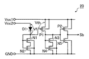
次に、アナログ電源監視部20の内部構成及び動作について、詳細な説明を行う。
Next, the internal configuration and operation of the analog power
図3は、アナログ電源監視部20の一構成例を示すブロック図である。
FIG. 3 is a block diagram illustrating a configuration example of the analog power
図3に示すように、本構成例のアナログ電源監視部20は、ダイオードD1と、Pチャネル型MOS電界効果トランジスタP1及びP2と、Nチャネル型MOS電界効果トランジスタN1〜N5と、を有して成る。
As shown in FIG. 3, the analog power
ダイオードD1のアノードは、第2電源電圧Vcc2の印加端に接続されている。ダイオードD1のカソードは、トランジスタN1のドレインに接続されている。トランジスタN1のソースは、トランジスタN2のドレインに接続されている。トランジスタN2のソースは、接地端に接続されている。トランジスタN1、N2のゲートは、いずれもダイオードD1のカソードに接続されている。トランジスタN1、N2のバックゲートは、いずれも接地端に接続されている。 The anode of the diode D1 is connected to the application terminal of the second power supply voltage Vcc2. The cathode of the diode D1 is connected to the drain of the transistor N1. The source of the transistor N1 is connected to the drain of the transistor N2. The source of the transistor N2 is connected to the ground terminal. The gates of the transistors N1 and N2 are both connected to the cathode of the diode D1. The back gates of the transistors N1 and N2 are both connected to the ground terminal.
トランジスタP1のソース及びバックゲートは、いずれも第1電源電圧Vcc1の印加端に接続されている。トランジスタP1のゲートは、ダイオードD1のカソードに接続されている。トランジスタP1のドレインは、トランジスタN3のドレインに接続されている。トランジスタN3のソースは、トランジスタN4のドレインに接続されている。トランジスタN4のソースは、接地端に接続されている。トランジスタN3、N4のゲートはいずれもトランジスタP1のドレインに接続されている。トランジスタN3、N4のバックゲートは、いずれも接地端に接続されている。 The source and back gate of the transistor P1 are both connected to the application terminal for the first power supply voltage Vcc1. The gate of the transistor P1 is connected to the cathode of the diode D1. The drain of the transistor P1 is connected to the drain of the transistor N3. The source of the transistor N3 is connected to the drain of the transistor N4. The source of the transistor N4 is connected to the ground terminal. The gates of the transistors N3 and N4 are both connected to the drain of the transistor P1. The back gates of the transistors N3 and N4 are both connected to the ground terminal.
トランジスタP2のソース及びバックゲートは、いずれも第1電源電圧Vcc1の印加端に接続されている。トランジスタP2のゲートは、トランジスタP1のドレインに接続されている。トランジスタP2のドレインは、トランジスタN5のドレインに接続される一方、モニタ信号Saの出力端として、論理積演算器21(図3では不図示)の入力端にも接続されている。トランジスタN5のソース及びバックゲートは、接地端に接続されている。トランジスタN5のゲートは、トランジスタP1のドレインに接続されている。 The source and back gate of the transistor P2 are both connected to the application terminal for the first power supply voltage Vcc1. The gate of the transistor P2 is connected to the drain of the transistor P1. The drain of the transistor P2 is connected to the drain of the transistor N5, and is also connected to the input terminal of the AND operator 21 (not shown in FIG. 3) as the output terminal of the monitor signal Sa. The source and back gate of the transistor N5 are connected to the ground terminal. The gate of the transistor N5 is connected to the drain of the transistor P1.
上記構成から成るアナログ電源監視部20において、トランジスタP1のゲートには、第2電源電圧Vcc2よりもダイオードD1の順方向降下電圧Vf(約0.6[V])だけ低い電圧(Vcc2−Vf)が印加されており、液晶表示装置の電源オン時には、第2電源電圧Vcc2が2.8[V]に維持されるので、トランジスタP1のゲート電圧は、約2.2[V]に維持される。一方、トランジスタP1のソースには、第1電源電圧Vcc1が印加されており、液晶表示装置の電源オン時には、第1電源電圧Vcc1が1.8[V]に維持されるので、トランジスタP1のソース電圧も1.8[V]に維持される。
In the analog power
従って、液晶表示装置の電源オン時には、トランジスタP1のゲート電圧がソース電圧よりも高くなるため、トランジスタP1はオフとなり、トランジスタP1のドレイン電圧は、トランジスタN3、N4を介してローレベルとなる。その結果、トランジスタP2がオンとなり、トランジスタN5がオフとなるので、モニタ信号Saはハイレベルとなる。 Therefore, when the liquid crystal display device is turned on, the gate voltage of the transistor P1 is higher than the source voltage, so that the transistor P1 is turned off, and the drain voltage of the transistor P1 is at a low level via the transistors N3 and N4. As a result, the transistor P2 is turned on and the transistor N5 is turned off, so that the monitor signal Sa becomes high level.
一方、液晶表示装置の動作中に電池が取り外された場合など、通常とは異なるシーケンスで電源がオフされたことに伴って、第2電源電圧Vcc2が低下し、トランジスタP1のゲート電圧(Vcc2−Vf)がトランジスタP1のソース電圧Vcc1よりもトランジスタP1のオンスレッショルド電圧Vth(約0.6[V])だけ低くなると、トランジスタP1がオンとなり、トランジスタP1のドレイン電圧は、第1電源電圧Vcc1に吊られてハイレベルとなる。その結果、トランジスタP2がオフとなり、トランジスタN5がオンとなるので、モニタ信号Saはローレベルとなる。 On the other hand, when the battery is removed during the operation of the liquid crystal display device, the second power supply voltage Vcc2 is lowered due to the power supply being turned off in an unusual sequence, and the gate voltage (Vcc2- When Vf) becomes lower than the source voltage Vcc1 of the transistor P1 by the on-threshold voltage Vth (about 0.6 [V]) of the transistor P1, the transistor P1 is turned on, and the drain voltage of the transistor P1 becomes the first power supply voltage Vcc1. Suspended to high level. As a result, the transistor P2 is turned off and the transistor N5 is turned on, so that the monitor signal Sa becomes low level.
なお、ダイオードD1を用いず、第2電源電圧Vcc2をトランジスタP1のゲートに直接印加する構成では、トランジスタP1がオフからオンに転じる時点で、第2電源電圧Vcc2がアナログ回路系の最低動作保証電圧を下回っているおそれがあるため、液晶セルの放電処理を確実に行うためには、図3に示した回路構成を採用することが望ましい。 In the configuration in which the second power supply voltage Vcc2 is directly applied to the gate of the transistor P1 without using the diode D1, the second power supply voltage Vcc2 is the minimum operation guarantee voltage of the analog circuit system when the transistor P1 turns from off to on. Therefore, it is desirable to employ the circuit configuration shown in FIG. 3 in order to reliably perform the discharge process of the liquid crystal cell.
このように、上記構成から成るアナログ電源監視部20であれば、ダイオードD1の順方向降下電圧Vfを利用することにより、第2電源電圧Vcc2が実使用範囲よりも大幅に低下した場合であって、かつ、第2電源電圧Vcc2がアナログ回路系の最低動作保証電圧を下回る前に、モニタ信号Saの論理をハイレベルからローレベルに変遷させることができるので、液晶表示装置の電源オフに際して、ノイズなどの影響を受けることなく、確実に液晶セルの放電処理を実行することが可能となる。
Thus, in the case of the analog power
なお、上記の実施形態では、本発明を単純マトリクス型の液晶表示パネルを駆動する液晶表示装置に適用した場合を例示して説明を行ったが、本発明の適用対象はこれに限定されるものではなく、その他形式の液晶表示パネルを駆動する液晶表示装置はもちろん、その他の機器に搭載される電源装置全般についても、本発明を適用することが可能である。 In the above embodiment, the case where the present invention is applied to a liquid crystal display device that drives a simple matrix type liquid crystal display panel has been described as an example. However, the scope of application of the present invention is not limited to this. Instead, the present invention can be applied not only to liquid crystal display devices that drive other types of liquid crystal display panels but also to power supply devices that are mounted on other devices.
また、本発明の構成は、上記実施形態のほか、発明の主旨を逸脱しない範囲で種々の変更を加えることが可能である。 The configuration of the present invention can be variously modified within the scope of the present invention in addition to the above embodiment.
例えば、上記実施形態では、モニタ信号Saと外部リセット信号Sbの論理演算信号を生成する論理ゲート部として、論理積演算器21を用いた構成を例に挙げて説明を行ったが、本発明の構成はこれに限定されるものではなく、その余の論理ゲート部を用いてもよいし、或いは、モニタ信号Saをロジック部11に直接入力する構成としても構わない。
For example, in the above-described embodiment, the configuration using the AND
本発明は、例えば、電池駆動の液晶駆動装置において、電源オフ時の意図しないライン表示を防止する上で有用な技術である。 The present invention is a technique useful for preventing unintended line display when the power is turned off, for example, in a battery-driven liquid crystal driving device.
1 液晶駆動装置(容量負荷駆動装置)
11 ロジック部
12 メモリ部
13 セグメントドライバ部
14 コモンドライバ部
15 電源部
20 アナログ電源監視部
21 論理積演算器
22 リセット信号生成部
2 液晶表示パネル
D1 ダイオード
P1、P2 Pチャネル型MOS電界効果トランジスタ
N1〜N5 Nチャネル型MOS電界効果トランジスタ
1 Liquid crystal drive (capacitive load drive)
DESCRIPTION OF
Claims (3)
第1電源電圧を駆動電圧とし、前記モニタ信号に応じてリセットリクエスト信号を生成するロジック部と;
第2電源電圧を駆動電圧とし、前記リセットリクエスト信号に応じてリセット信号を生成するリセット信号生成部と;
第2電源電圧を駆動電圧とし、前記リセット信号に応じて液晶セルの放電処理を行うドライバ部と;
を有して成り、
前記電源監視部は、
アノードが第2電源電圧の印加端に接続されたダイオードと、
ソース及びバックゲートが第1電源電圧の印加端に接続され、ゲートが前記ダイオードのカソードに接続された第1Pチャネル型電界効果トランジスタと、
ソース及びバックゲートが第1電源電圧の印加端に接続され、ゲートが第1Pチャネル型電界効果トランジスタのドレインに接続され、ソースが前記モニタ信号の出力端に接続された第2Pチャネル型電界効果トランジスタと、
ドレイン及びゲートが前記ダイオードのカソードに接続され、バックゲートが接地端に接続された第1Nチャネル型電界効果トランジスタと、
ドレインが第1Nチャネル型電界効果トランジスタのソースに接続され、ゲートが前記ダイオードのカソードに接続され、ソース及びバックゲートが接地端に接続された第2Nチャネル型電界効果トランジスタと、
ドレイン及びゲートが第1Pチャネル型電界効果トランジスタのドレインに接続され、バックゲートが接地端に接続された第3Nチャネル型電界効果トランジスタと、
ドレインが第3Nチャネル型電界効果トランジスタのソースに接続され、ゲートが第1Pチャネル型電界効果トランジスタのドレインに接続され、ソース及びバックゲートが接地端に接続された第4Nチャネル型電界効果トランジスタと、
ドレインが前記モニタ信号の出力端に接続され、ゲートが第1Pチャネル型電界効果トランジスタのドレインに接続され、ソース及びバックゲートが接地端に接続された第5Nチャネル型電界効果トランジスタと、
を有して成り、前記第1Pチャネル型電界効果トランジスタのドレイン電圧に応じて前記モニタ信号の論理変遷を行うことを特徴とする液晶駆動装置。 A power supply monitoring unit that uses the first power supply voltage as a drive voltage, monitors a second power supply voltage that is higher than the first power supply voltage, and generates a monitor signal indicating whether or not the second power supply voltage is below a predetermined threshold;
A logic unit that uses the first power supply voltage as a drive voltage and generates a reset request signal according to the monitor signal;
A reset signal generating unit that uses the second power supply voltage as a drive voltage and generates a reset signal in response to the reset request signal;
A driver unit that uses the second power supply voltage as a driving voltage and performs discharge processing of the liquid crystal cell in response to the reset signal;
Ri formed have,
The power monitoring unit
A diode having an anode connected to the application terminal of the second power supply voltage;
A first P-channel field effect transistor having a source and a back gate connected to a first power supply voltage application end and a gate connected to the cathode of the diode;
A second P-channel field effect transistor having a source and a back gate connected to a first power supply voltage application terminal, a gate connected to the drain of the first P-channel field effect transistor, and a source connected to the output terminal of the monitor signal When,
A first N-channel field effect transistor having a drain and a gate connected to the cathode of the diode and a back gate connected to a ground terminal;
A second N-channel field effect transistor having a drain connected to the source of the first N-channel field effect transistor, a gate connected to the cathode of the diode, and a source and a back gate connected to a ground terminal;
A third N-channel field effect transistor having a drain and a gate connected to the drain of the first P-channel field effect transistor and a back gate connected to the ground terminal;
A fourth N-channel field effect transistor having a drain connected to the source of the third N-channel field effect transistor, a gate connected to the drain of the first P-channel field-effect transistor, and a source and a back gate connected to the ground terminal;
A fifth N-channel field effect transistor having a drain connected to the output terminal of the monitor signal, a gate connected to the drain of the first P-channel field effect transistor, and a source and a back gate connected to the ground terminal;
A liquid crystal driving device comprising: a logic transition of the monitor signal in accordance with a drain voltage of the first P-channel field effect transistor .
Priority Applications (3)
| Application Number | Priority Date | Filing Date | Title |
|---|---|---|---|
| JP2007277160A JP5118939B2 (en) | 2007-10-25 | 2007-10-25 | Liquid crystal drive device and liquid crystal display device using the same |
| CNA2008101868942A CN101452687A (en) | 2007-10-25 | 2008-10-23 | Liquid crystal driving device, and liquid crystal display device using same |
| US12/256,656 US20090153538A1 (en) | 2007-10-25 | 2008-10-23 | Liquid crystal driving device, and liquid crystal display device using same |
Applications Claiming Priority (1)
| Application Number | Priority Date | Filing Date | Title |
|---|---|---|---|
| JP2007277160A JP5118939B2 (en) | 2007-10-25 | 2007-10-25 | Liquid crystal drive device and liquid crystal display device using the same |
Publications (2)
| Publication Number | Publication Date |
|---|---|
| JP2009104014A JP2009104014A (en) | 2009-05-14 |
| JP5118939B2 true JP5118939B2 (en) | 2013-01-16 |
Family
ID=40705730
Family Applications (1)
| Application Number | Title | Priority Date | Filing Date |
|---|---|---|---|
| JP2007277160A Expired - Fee Related JP5118939B2 (en) | 2007-10-25 | 2007-10-25 | Liquid crystal drive device and liquid crystal display device using the same |
Country Status (3)
| Country | Link |
|---|---|
| US (1) | US20090153538A1 (en) |
| JP (1) | JP5118939B2 (en) |
| CN (1) | CN101452687A (en) |
Families Citing this family (7)
| Publication number | Priority date | Publication date | Assignee | Title |
|---|---|---|---|---|
| KR101651548B1 (en) | 2010-02-18 | 2016-09-05 | 삼성전자주식회사 | Method for driving a liquid crystal panel, Source driver and Liquid crystal display system for using the method |
| JP2014056095A (en) * | 2012-09-12 | 2014-03-27 | Sharp Corp | Liquid crystal display device |
| JP2016170303A (en) * | 2015-03-13 | 2016-09-23 | シナプティクス・ジャパン合同会社 | Semiconductor device and electronic equipment |
| KR102400194B1 (en) | 2015-10-12 | 2022-05-18 | 삼성전자주식회사 | Display driving circuit and display device comprising the same |
| TWI560673B (en) * | 2015-12-02 | 2016-12-01 | Au Optronics Corp | Power supply circuit and driving method of display panel |
| CN106548761B (en) * | 2017-01-17 | 2019-01-18 | 京东方科技集团股份有限公司 | A kind of display control circuit of display panel, display control method and relevant apparatus |
| US11112628B2 (en) | 2017-06-16 | 2021-09-07 | Sharp Kabushiki Kaisha | Liquid crystal display device including common electrode control circuit |
Family Cites Families (18)
| Publication number | Priority date | Publication date | Assignee | Title |
|---|---|---|---|---|
| JPH08154334A (en) * | 1994-11-28 | 1996-06-11 | Sanyo Electric Co Ltd | Power supply voltage detector |
| KR100206567B1 (en) * | 1995-09-07 | 1999-07-01 | 윤종용 | Screen erase circuit and its driving method of tft |
| KR100430095B1 (en) * | 1998-09-15 | 2004-07-27 | 엘지.필립스 엘시디 주식회사 | Apparatus For Eliminating Afterimage in Liquid Crystal Display and Method Thereof |
| JP3179444B2 (en) * | 1999-04-22 | 2001-06-25 | 日本電気アイシーマイコンシステム株式会社 | Power supply monitoring circuit |
| KR100405026B1 (en) * | 2000-12-22 | 2003-11-07 | 엘지.필립스 엘시디 주식회사 | Liquid Crystal Display |
| JP3856714B2 (en) * | 2002-03-06 | 2006-12-13 | 松下電器産業株式会社 | Semiconductor integrated circuit provided with potential detection circuit and signal transmission / reception system |
| JP4120409B2 (en) * | 2003-01-22 | 2008-07-16 | ソニー株式会社 | Liquid crystal display |
| JP2004335871A (en) * | 2003-05-09 | 2004-11-25 | Sharp Corp | Test method of integrated circuit, integrated circuit and liquid crystal driving device |
| JP2005030818A (en) * | 2003-07-09 | 2005-02-03 | Fujitsu Ten Ltd | Voltage monitoring circuit |
| JP2005043698A (en) * | 2003-07-23 | 2005-02-17 | Toshiba Matsushita Display Technology Co Ltd | Liquid crystal display |
| JP2005049651A (en) * | 2003-07-29 | 2005-02-24 | Iiyama Corp | Display device |
| TWI230371B (en) * | 2003-10-09 | 2005-04-01 | Toppoly Optoelectronics Corp | Circuit for clearing after image |
| KR100539264B1 (en) * | 2004-05-15 | 2005-12-27 | 삼성전자주식회사 | Detection circuit capable of removing source voltage and display device |
| US7679595B2 (en) * | 2004-07-30 | 2010-03-16 | Tpo Displays Corp. | Image sticking prevention circuit for display device |
| JP4089908B2 (en) * | 2004-09-08 | 2008-05-28 | 京セラミタ株式会社 | Liquid crystal display device and image forming apparatus |
| JP2006105810A (en) * | 2004-10-06 | 2006-04-20 | Sanyo Electric Co Ltd | Voltage detection circuit |
| JP2006211297A (en) * | 2005-01-28 | 2006-08-10 | Yokogawa Electric Corp | Voltage monitoring circuit |
| JP2007212689A (en) * | 2006-02-08 | 2007-08-23 | Toshiba Matsushita Display Technology Co Ltd | Liquid crystal display element |
-
2007
- 2007-10-25 JP JP2007277160A patent/JP5118939B2/en not_active Expired - Fee Related
-
2008
- 2008-10-23 US US12/256,656 patent/US20090153538A1/en not_active Abandoned
- 2008-10-23 CN CNA2008101868942A patent/CN101452687A/en active Pending
Also Published As
| Publication number | Publication date |
|---|---|
| US20090153538A1 (en) | 2009-06-18 |
| CN101452687A (en) | 2009-06-10 |
| JP2009104014A (en) | 2009-05-14 |
Similar Documents
| Publication | Publication Date | Title |
|---|---|---|
| JP5118939B2 (en) | Liquid crystal drive device and liquid crystal display device using the same | |
| CN101777320B (en) | Afterimage elimination circuit, display and electronic device | |
| US8872859B2 (en) | Liquid crystal panel driving method, and source driver and liquid crystal display apparatus using the method | |
| CN100492111C (en) | Discharge circuit and liquid crystal display device using the discharge circuit | |
| CN101604515B (en) | Discharge circuit and display device with the same | |
| CN107610632B (en) | Display driving circuit, power management device, display device and driving method thereof | |
| CN100514431C (en) | Circuit, method and display device for eliminating residual image | |
| US10497302B2 (en) | Display driving device and display device including the same | |
| US8368683B2 (en) | Power-off control circuit and liquid crystal display panel comprising the same | |
| US9281818B2 (en) | Interface circuit, and semiconductor device and liquid crystal display device including the same | |
| US20110292005A1 (en) | Display apparatus and method for eliminating ghost thereof | |
| US20150303925A1 (en) | Output Buffer, Gate Electrode Driving Circuit and Method for Controlling the Same | |
| US10008173B2 (en) | Liquid crystal display device with a discharge control circuit | |
| CN101882416A (en) | Display device and method for eliminating afterimage | |
| JP6730835B2 (en) | Overcurrent detection circuit | |
| CN101968945A (en) | Source driver and display apparatus comprising the same | |
| US10504478B2 (en) | Semiconductor device having shifted operation voltages in different modes and electronic apparatus thereof | |
| JP2006201760A (en) | Display device drive circuit and drive method | |
| KR101493487B1 (en) | Driving device and liquid crystal display device including the same and method of driving the same | |
| CN101556776A (en) | Driving circuit for realizing rapid discharge of pixel thin film transistor | |
| KR101338628B1 (en) | Discharge circuit and display device with the same | |
| US7453290B2 (en) | Supply voltage removal detecting circuit, display device and method for removing latent image | |
| KR20080010581A (en) | Plasma display device and its power off sequence method | |
| JP2004240062A (en) | Liquid crystal display device, method for stopping the same, program, and record medium |
Legal Events
| Date | Code | Title | Description |
|---|---|---|---|
| A621 | Written request for application examination |
Free format text: JAPANESE INTERMEDIATE CODE: A621 Effective date: 20101021 |
|
| A131 | Notification of reasons for refusal |
Free format text: JAPANESE INTERMEDIATE CODE: A131 Effective date: 20120724 |
|
| A521 | Request for written amendment filed |
Free format text: JAPANESE INTERMEDIATE CODE: A523 Effective date: 20120830 |
|
| TRDD | Decision of grant or rejection written | ||
| A01 | Written decision to grant a patent or to grant a registration (utility model) |
Free format text: JAPANESE INTERMEDIATE CODE: A01 Effective date: 20120925 |
|
| A01 | Written decision to grant a patent or to grant a registration (utility model) |
Free format text: JAPANESE INTERMEDIATE CODE: A01 |
|
| A61 | First payment of annual fees (during grant procedure) |
Free format text: JAPANESE INTERMEDIATE CODE: A61 Effective date: 20121022 |
|
| R150 | Certificate of patent or registration of utility model |
Free format text: JAPANESE INTERMEDIATE CODE: R150 |
|
| FPAY | Renewal fee payment (event date is renewal date of database) |
Free format text: PAYMENT UNTIL: 20151026 Year of fee payment: 3 |
|
| LAPS | Cancellation because of no payment of annual fees |