(第1実施形態)
本発明の第1実施形態による表示装置及びその製造方法について図1乃至図4を用いて説明する。図1は本実施形態による表示装置の構造を示す概略図、図2は有機エレクトロルミネッセンス素子を用いたボトムエミッション型の表示装置の構造を示す概略図、図3及び図4は本実施形態による表示装置の製造方法を示す工程断面図である。
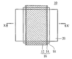
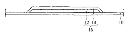
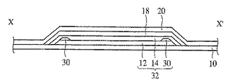
まず、本実施形態による表示装置の構造について図1を用いて説明する。図1Aは本実施形態による表示装置の構造を示す平面図、図1Bは図1AのX−X′線断面図である。本実施形態による表示装置は、絶縁性基板上に形成された有機エレクトロルミネッセンス素子を有するパッシブマトリクス型の表示装置である。なお、図1は1画素分の構造を示したものであるが、実際には複数の画素がマトリクス状に配置されている。
図1Bに示すように、ガラス基板よりなる絶縁性基板10上には、光反射性を有するAl膜よりなる光反射膜12が形成されている。光反射膜12上には、光透過性を有するITO膜よりなる透明導電膜14が形成されている。なお、本願明細書において、「光反射性を有する」とは、光の反射率が50%以上、より好ましくは80%以上であることを意味する。また、「光透過性を有する」とは、光の透過率が50%以上、より好ましくは80%以上であることを意味する。こうして、絶縁性基板10上に、光反射膜12と透明導電膜14とを有するアノード電極16が形成されている。アノード電極16上には、正孔注入層と、正孔輸送層と、発光層と、電子輸送層と、電子注入層とが順次積層されてなる有機エレクトロルミネッセンス層18が形成されている。有機エレクトロルミネッセンス層18上には、光透過性を有するAl/ITO積層膜よりなるカソード電極20が形成されている。こうして、絶縁性基板10上に、アノード電極16と、有機エレクトロルミネッセンス層18と、カソード電極20とを有する有機エレクトロルミネッセンス素子が形成されている。
図1Aに示すように、アノード電極16は、絶縁性基板10上に、所定の方向(図1A中上下方向)に延在して形成されている。透明導電膜14は、光反射膜12よりも幅広に形成されている。これにより、光反射膜12は、透明導電膜14により覆われている。カソード電極20は、アノード電極16が形成された絶縁性基板10上に、アノード電極16に直交する方向(図1A中左右方向)に延在して形成されている。これらアノード電極16とカソード電極20とが交差する領域の両者の間に、交差領域よりも幅広の矩形状に有機エレクトロルミネッセンス層18が形成されている。こうして、上記構造を有する有機エレクトロルミネッセンス素子が形成された画素領域が構成されている。
本実施形態による表示装置は、有機エレクトロルミネッセンス素子において、光反射性を有する光反射膜12と、光透過性を有する透明導電膜14とをアノード電極16が有し、光反射膜12が透明導電膜14により覆われていることに主たる特徴がある。
本実施形態による表示装置では、カソード電極20から電子が有機エレクトロルミネッセンス層18に注入され、アノード電極16の透明導電膜14から正孔が有機エレクトロルミネッセンス層18に注入される。注入された電子は電子輸送層により発光層に輸送され、注入された正孔は正孔輸送層により発光層に輸送される。こうして発光層に輸送された電子と正孔とが、発光層において再結合することにより発光が生じる。発光層において発生した光は、光反射膜12によりカソード電極20側に反射され、光透過性を有するカソード電極20側から取り出される。
このように、本実施形態による表示装置は、光反射膜12の存在により、絶縁性基板10とは反対側のカソード電極20側から光が取り出されるトップエミッション型となっている。したがって、絶縁性基板10と有機エレクトロルミネッセンス素子との間に他の素子が形成される場合において、他の素子が形成された領域からも光を取り出すことが可能となる。すなわち、有機エレクトロルミネッセンス素子の発光面積が他の素子により制限されることはなく、高い発光効率を実現することができる。例えば、薄膜トランジスタ等のスイッチング素子が形成された絶縁性基板上に層間絶縁膜を介して有機エレクトロルミネッセンス素子を形成する場合において、スイッチング素子により発光面積が制限されることはなく、高い発光効率を実現することができる。
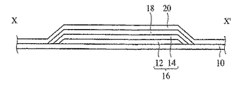
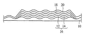
このようなトップエミッション型の本実施形態による表示装置に対して、図2に示す表示装置は、有機エレクトロルミネッセンス素子を用いたボトムエミッション型の表示装置である。図2Aは有機エレクトロルミネッセンス素子を用いたボトムエミッション型の表示装置の構造を示す平面図、図2Bは図2AのX−X′線断面図である。なお、図2は1画素分の構造を示したものであるが、実際には複数の画素がマトリクス状に配置されている。
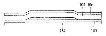
図2に示すように、ガラス基板よりなる絶縁性基板100上には、ITO膜よりなる透明なアノード電極102が形成されている。アノード電極102上には、正孔輸送層と、発光層と、電子輸送層とが順次積層されてなる有機エレクトロルミネッセンス層104が形成されている。有機エレクトロルミネッセンス層104上には、Al膜やMg−Ag合金膜等よりなるカソード電極106が形成されている。こうして、絶縁性基板100上に、アノード電極102と、有機エレクトロルミネッセンス層104と、カソード電極106とを有する有機エレクトロルミネッセンス素子が形成されている。
図2に示すボトムエミッション型の表示装置では、有機エレクトロルミネッセンス層104において発生した光は、絶縁性基板100側から取り出される。このため、絶縁性基板10と有機エレクトロルミネッセンス素子との間にスイッチング素子等の他の素子が形成される場合に、有機エレクトロルミネッセンス素子の発光面積が他の素子により制限され、本実施形態による表示装置のように高い発光効率を実現することは困難である。
また、本実施形態による表示装置は、アノード電極16において、Al膜よりなる光反射膜12は、その表面が剥き出しにならないように、ITO膜よりなる透明導電膜14により覆われている。これにより、製造工程におけるITO膜をパターニングする際に、Al膜よりなる光反射膜12が腐食されるのを防止することができる。すなわち、ITO膜のパターニングにはアルカリ性の現像液が用いられるため、Al膜の表面が露出しAl膜及びITO膜の両者が現像液に曝されると、電池効果によりAl膜が腐食されることがある。本実施形態による表示装置では、Al膜よりなる光反射膜12を覆うようにITO膜よりなる透明導電膜14が形成されているため、かかる電池効果による光反射膜12の腐食が防止されている。
また、Al膜よりなる光反射膜12とITO膜よりなる透明導電膜14との間には、有機エレクトロルミネッセンス素子に対する駆動電圧の印加時の発熱等によりウィスカーが発生する場合がある。このようなウィスカーは電極間の短絡の原因の1つになり得るものである。しかしながら、本実施形態による表示装置では、Al膜よりなる光反射膜12を覆うようにITO膜よりなる透明導電膜14が形成されているため、ウィスカーによるアノード電極16とカソード電極20との間の短絡を防止することができる。
なお、Al膜は、従来用いられていたCr膜よりも高い反射率を有しており、有機エレクトロルミネッセンス素子の光反射膜として好適である。その一方、光反射膜としてAl膜を用いる場合、上述のような課題が発生する。本実施形態による表示装置は、Al膜を覆うようにITO膜を形成することにより、腐食や電極間の短絡等の不都合を伴うことなく従来よりも高い発光効率を実現するものである。
さらに、有機エレクトロルミネッセンス層18は、従来の有機エレクトロルミネッセンス素子と同様に、ITO膜よりなる透明導電膜14上に形成されている。このため、有機エレクトロルミネッセンス層18として、従来の有機エレクトロルミネッセンス素子と同様の材料及び構造の有機エレクトロルミネッセンス層をそのまま用いて高い発光効率を有するトップエミッション型の表示装置を構成することができる。
次に、本実施形態による表示装置の製造方法について図3及び図4を用いて説明する。
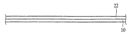
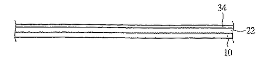
まず、ガラス基板よりなる絶縁性基板10上に、例えばスパッタ法により、例えば膜厚150nmのAl膜22を形成する(図3Aを参照)。
次いで、フォトリソグラフィー及びエッチングにより、Al膜22を所定の形状にパターニングする。こうして、絶縁性基板10上に、Al膜22よりなる光反射膜12を形成する(図3Bを参照)。
次いで、光反射膜12が形成された絶縁性基板10上に、例えばスパッタ法により、例えば膜厚70nmのITO膜24を形成する(図3Cを参照)。
次いで、フォトリソグラフィー及びエッチングにより、ITO膜24を所定の形状にパターニングする。このとき、光反射膜12の表面が剥き出しにならないように、光反射膜12を被覆する形状及び大きさにITO膜24をパターニングする。こうして、ITO膜24よりなる透明導電膜14を形成する(図4Aを参照)。ITO膜24をパターニングする間、ITO膜24下のAl膜22よりなる光反射膜12の表面が露出することはないので、電池効果による光反射膜12の腐食を防止することができる。
次いで、光反射膜12と透明導電膜14とを有するアノード電極16が形成された絶縁性基板10上に、例えば真空蒸着法により、所定の大きさに開口された蒸着マスクを介して、例えば膜厚40nmの2−TNATA(4,4’,4’’−トリス(2−ナフチルフェニルアミノ)トリフェニルアミン)膜と、例えば膜厚10nmのα−NPD(N,N’−ジナフチル−N,N’−ジフェニル−[1,1’−ビフェニル]−4,4’−ジアミン)膜と、例えば少量のt(npa)py(1,3,6,8−テトラ(N−ナフチル−N’−フェニルアミノ)ピレン)をドープした例えば膜厚30nmのAlq3(トリス(8−ヒドロキシキノリナート)アルミニウム)膜と、例えば膜厚20nmのAlq3膜と、例えば0.5nmのLiF膜とを順次形成する。
こうして、2−TNATA膜よりなる正孔注入層と、α−NPD膜よりなる正孔輸送層と、t(npa)pyをドープしたAlq3膜よりなる発光層と、Alq3膜よりなる電子輸送層と、LiF膜よりなる電子注入層とを有する有機エレクトロルミネッセンス層18を形成する(図4Bを参照)。
次いで、有機エレクトロルミネッセンス層18が形成された絶縁性基板10上に、例えば真空蒸着法及びスパッタ法により、所定の形状に開口されたマスクを介して、例えば膜厚10nmのAl膜と、例えば膜厚30nmのITO膜とを順次形成し、Al/ITO積層膜を形成する。
こうして、Al/ITO積層膜よりなるカソード電極20を形成する(図4Cを参照)。
こうして、図1に示す表示装置が製造される。
このように、本実施形態によれば、有機エレクトロルミネッセンス素子を用いた表示装置において、光反射性を有する光反射膜12と、光透過性を有する透明導電膜14とをアノード電極16が有するので、高い発光効率を有するトップエミッション型の表示装置を実現することができる。
また、光反射膜12が透明導電膜14により覆われているので、光反射膜12の腐食や、光反射膜12と透明導電膜14との間に生じるウィスカー等による素子特性の劣化を抑制することができる。
また、有機エレクトロルミネッセンス層18は従来の有機エレクトロルミネッセンス素子と同様に透明導電膜14上に形成されるため、有機エレクトロルミネッセンス層18として、従来の有機エレクトロルミネッセンス素子と同様の材料及び構造の有機エレクトロルミネッセンス層をそのまま用いることができる。
(第2実施形態)
本発明の第2実施形態による表示装置について図5乃至図7を用いて説明する。図5は本実施形態による表示装置の構造を示す概略図、図6及び図7は本実施形態による表示装置の製造方法を示す工程断面図である。なお、図1、図3、及び図4に示す第1実施形態による表示装置及びその製造方法と同様の構成要素については同一の符号を付し説明を省略し或いは簡略にする。
本実施形態による表示装置は、第1実施形態による表示装置と同様に、絶縁性基板上に形成された有機エレクトロルミネッセンス素子を有するパッシブマトリクス型の表示装置であり、その基本的構成は、第1実施形態による表示装置と同様である。本実施形態による表示装置は、光反射膜12と、透明導電膜14との間の導通が確保され、光反射膜12からの正孔の注入が可能となっている点で、第1実施形態による表示装置と異なっている。
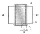
まず、本実施形態による表示装置の構造について図5を用いて説明する。図5Aは本実施形態による表示装置の構造を示す平面図、図5Bは図5AのX−X′線断面図である。なお、図5は1画素分の構造を示したものであるが、実際には複数の画素がマトリクス状に配置されている。
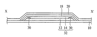
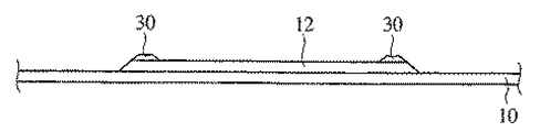
図5Bに示すように、ガラス基板よりなる絶縁性基板10上には、光反射性を有するAl膜よりなる光反射膜12が形成されている。光反射膜12の周縁部上には、光反射性を有するMo(モリブデン)膜よりなる介在膜30が形成されている。周縁部上に介在膜30が形成された光反射膜12上には、光透過性を有するITO膜よりなる透明導電膜14が形成されている。介在膜30は光反射膜12及び透明導電膜14のそれぞれに電気的に接続するものであり、この介在膜30により、透明導電膜14と光反射膜12との電気的接続が改善され、両者の間の導通が確保されている。こうして、絶縁性基板10上に、光反射膜12と、透明導電膜14と、両者の電気的接続を改善する介在膜30とを有するアノード電極32が形成されている。アノード電極32上には、正孔注入層と、正孔輸送層と、発光層と、電子輸送層と、電子注入層とが順次積層されてなる有機エレクトロルミネッセンス層18が形成されている。有機エレクトロルミネッセンス層18上には、光透過性を有するAl/ITO積層膜よりなるカソード電極20が形成されている。こうして、絶縁性基板10上に、アノード電極32と、有機エレクトロルミネッセンス層18と、カソード電極20とを有する有機エレクトロルミネッセンス素子が形成されている。
図5Aに示すように、アノード電極32は、絶縁性基板10上に、所定の方向(図5A中上下方向)に延在して形成されている。介在膜30は、光反射膜12の周縁部上に枠状に形成されている。透明導電膜14は、介在膜30が形成された光反射膜12よりも幅広に形成されている。これにより、介在膜30が形成された光反射膜12は、透明導電膜14により覆われている。カソード電極20は、アノード電極16が形成された絶縁性基板10上に、アノード電極16に直交する方向(図5A中左右方向)に延在して形成されている。これらアノード電極32とカソード電極20とが交差する領域の両者の間に、交差領域よりも幅広の矩形状に有機エレクトロルミネッセンス層18が形成されている。こうして、上記構造を有する有機エレクトロルミネッセンス素子が形成された画素領域が構成されている。
本実施形態による表示装置は、有機エレクトロルミネッセンス素子において、光反射性を有する光反射膜12と、光反射膜12の周縁部上に形成され、光反射膜12及び光反射膜12上に形成される透明導電膜14のそれぞれに電気的に接続し、両者の間の導通を確保するための介在膜30と、介在膜30が周縁部上に形成された光反射膜12上に形成された光透過性を有する透明導電膜14とをアノード電極32が有し、光反射膜12が透明導電膜14により覆われていることに主たる特徴がある。
Al膜とITO膜とは電気的接続が良好ではないため、第1実施形態による表示装置では、アノード電極16において、Al膜よりなる光反射膜12とITO膜よりなる透明導電膜14との間の導通が充分に確保されない場合がある。
本実施形態による表示装置では、アノード電極32の周縁部がAl/Mo/ITO構造となっている。このため、Al膜及びITO膜のそれぞれに電気的に接続するMo膜よりなる介在膜30により、Al膜よりなる光反射膜12とITO膜よりなる透明導電膜14との間の電気的接続が改善され、両者の間の導通が確保されている。したがって、光反射膜12から正孔を有機エレクトロルミネッセンス層18に注入することができる。また、介在膜30は光反射膜12の周縁部上に形成されているため、介在膜30よりも反射率の高い光反射膜12により有機エレクトロルミネッセンス層18の発光層において発生した光をカソード電極20側に充分に反射することができる。
また、周縁部上に介在膜30が形成された光反射膜12を覆うように透明導電膜14が形成されているため、第1実施形態による表示装置と同様に、光反射膜12の腐食を防止することができる。また、駆動電圧印加時の発熱等により光反射膜12と透明導電膜14との間に生じるウィスカーによるアノード電極32とカソード電極20との間の短絡を防止することができる。また、有機エレクトロルミネッセンス層18には従来の有機エレクトロルミネッセンス素子の有機エレクトロルミネッセンス層をそのまま用いることができる。
次に、本実施形態による表示装置の製造方法について図6及び図7を用いて説明する。
まず、ガラス基板よりなる絶縁性基板10上に、例えばスパッタ法により、例えば膜厚150nmのAl膜22を形成する。
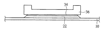
次いで、Al膜22上に、例えばスパッタ法により、例えば膜厚10nmのMo膜34を形成する(図6Aを参照)。
次いで、Mo膜34上に、例えばスピンコート法により、レジスト膜36を形成する。この後、フォトリソグラフィーを用いてレジスト膜36をパターニングすることにより、Al膜22を残存させるべき光反射膜12の形成予定領域を覆うように、レジスト膜36を残存させる。このとき、Mo膜34を残存させるべき介在膜30の形成予定領域を覆うレジスト膜36の周縁部の膜厚が厚く、Mo膜34を除去しAl膜22を残存させるべき領域を覆うレジスト膜36の周縁部以外の部分の膜厚が薄くなるように、レジスト膜36を残存させる(図6Bを参照)。
上記のレジスト膜36の膜厚の厚薄の設定は、例えばフォトリソグラフィーに用いるマスクで露光量を調整することに行うことができる。具体的には、例えば、フォトリソグラフィーに用いるマスクにおいて、Mo膜34を残存させるべき介在膜30の形成予定領域を覆うレジスト膜36を露光する部分を通常の開口にする一方、Mo膜34を除去しAl膜22を残存させるべき領域を覆うレジスト膜36を露光する部分をスリット状にする。このようなマスクを用いてレジスト膜36を現像すると、Mo膜34を除去しAl膜22を残存させるべき領域を覆うレジスト膜36は、介在膜30の形成予定領域を覆うレジスト膜36と比較して露光が不十分なものとなる。このように、レジスト膜36の露光量を部分的に変えて現像することにより、レジスト膜36の膜厚に厚薄を設けることができる。
次いで、膜厚に厚薄が設けられたレジスト膜36をマスクとして、例えばウェットエッチングにより、アノード電極32の形成領域以外の不要なAl膜22、Mo膜34を除去する(図6Cを参照)。ウェットエッチングには、例えば、リン酸、硝酸、酢酸、及び水を混合したエッチング液を用いることができる。
次いで、例えばアッシング処理によりレジスト膜36をエッチバックし、Mo膜34を除去しAl膜22を残存させるべき領域を覆うレジスト膜36の膜厚の薄い部分を除去して、レジスト膜36に開口部38を形成する。一方、介在膜30の形成予定領域を覆うレジスト膜36の膜厚の厚い部分は残存させる(図6Dを参照)。
次いで、開口部38が形成されたレジスト膜36をマスクとして、例えばウェットエッチングにより、開口部38の底部に露出したMo膜34を除去する。ウェットエッチングには、図6Cにおいて不要なMo膜34及びAl膜22を除去した場合と同様に、例えば、例えば、リン酸、硝酸、酢酸、及び水を混合したエッチング液を用いることができる。
次いで、マスクとして用いたレジスト膜36を除去する。
こうして、Al膜22よりなる光反射膜12と、光反射膜12の周縁部上に形成されたMo膜34よりなる介在膜30とを形成する(図7Aを参照)。
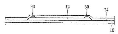
次いで、光反射膜12及び介在膜30が形成された絶縁性基板10上に、例えばスパッタ法により、例えば膜厚70nmのITO膜24を形成する(図7Bを参照)。
次いで、フォトリソグラフィー及びエッチングにより、ITO膜24を所定の形状にパターニングする。このとき、介在膜30が周縁部上に形成された光反射膜12の表面が剥き出しにならないように、光反射膜12を被覆する形状及び大きさにITO膜24をパターニングする。こうして、ITO膜24よりなる透明導電膜14を形成する(図7Cを参照)。
以後、図4B及び図4Cに示す第1実施形態による表示装置の製造方法と同様にして有機エレクトロルミネッセンス層18、カソード電極20をそれぞれ形成することにより、図5に示す本実施形態による表示装置が製造される。
このように、本実施形態によれば、有機エレクトロルミネッセンス素子を用いた表示装置において、光反射性を有する光反射膜12と、光透過性を有する透明導電膜14とをアノード電極32が有するので、高い発光効率を有するトップエミッション型の表示装置を実現することができる。
また、光反射膜12が透明導電膜14により覆われているので、光反射膜12の腐食や、光反射膜12と透明導電膜14との間に生じるウィスカー等による素子特性の劣化を抑制することができる。
さらに、光反射膜12の周縁部上には、光反射膜12及び光反射膜12上に形成される透明導電膜14のそれぞれに電気的に接続し、両者の間の導通を確保するための介在膜30が形成されているため、光反射膜12から正孔を有機エレクトロルミネッセンス層18に注入することができる。
また、有機エレクトロルミネッセンス層18は従来の有機エレクトロルミネッセンス素子と同様に透明導電膜14上に形成されるため、有機エレクトロルミネッセンス層18として、従来の有機エレクトロルミネッセンス素子と同様の材料及び構造の有機エレクトロルミネッセンス層をそのまま用いることができる。
(第3実施形態)
本発明の第3実施形態による表示装置及びその製造方法について図8を用いて説明する。図8は本実施形態による表示装置の構造を示す概略図である。なお、図1及び図5にそれぞれ示す第1及び第2実施形態による表示装置と同様の構成要素については同一の符号を付し説明を省略し或いは簡略にする。
本実施形態による表示装置は、絶縁性基板上に形成された有機エレクトロルミネッセンス素子が形成された1画素内において、有機エレクトロルミネッセンス層の発光層で発生した光が絶縁性基板とは反対のカソード電極側から取り出される上面発光部と、有機エレクトロルミネッセンス層の発光層で発生した光がカソード電極側及び絶縁性基板側の両側から取り出される両面発光部とを有するパッシブマトリクス型の表示装置である。
以下、本実施形態による表示装置の構造について図8を用いて説明する。図8Aは本実施形態による表示装置の構造を示す平面図、図8Bは図8AのX−X′線断面図、図8Cは図8AのY−Y′線断面図である。なお、図8は1画素分の構造を示したものであるが、実際には複数の画素がマトリクス状に配置されている。
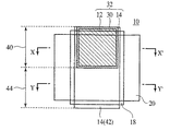
図8Aに示すように、ガラス基板よりなる絶縁性基板10上には、第1及び第2実施形態による表示装置と同様に、透明導電膜14と、有機エレクトロルミネッセンス層18と、カソード電極20とが形成されている。透明導電膜14とカソード電極20とが交差した画素領域は、透明導電膜14の延在方向に直交する境界により、ほぼ等面積の2つの領域に分けられている。境界の一方の側の領域には、透明導電膜14の下に光反射膜12が形成され、光反射膜12と透明導電膜14とを有するアノード電極32が形成された上面発光部40が設けられている。境界の他方の側の領域には、光反射膜12が形成されておらず、透明導電膜14よりなるアノード電極42が形成された両面発光部44が設けられている。
上面発光部40は、図8Bに示す断面構造を有している。図8Bに示す断面構造は、第2実施形態による表示装置と同様の断面構造となっている。すなわち、絶縁性基板10上には、光反射性を有するAl膜よりなる光反射膜12が形成されている。光反射膜12の周縁部上には、光反射性を有するMo膜よりなる介在膜30が形成されている。周縁部上に介在膜30が形成された光反射膜12上には、光透過性を有するITO膜よりなる透明導電膜14が形成されている。介在膜30は光反射膜12及び透明導電膜14のそれぞれに電気的に接続するものであり、この介在膜30により、透明導電膜14と光反射膜12との電気的接続が改善され、両者の間の導通が確保されている。こうして、絶縁性基板10上に、光反射膜12と、透明導電膜14と、両者の電気的接続を改善する介在膜30とを有するアノード電極32が形成されている。アノード電極32上には、正孔注入層と、正孔輸送層と、発光層と、電子輸送層と、電子注入層とが順次積層されてなる有機エレクトロルミネッセンス層18が形成されている。有機エレクトロルミネッセンス層18上には、光透過性を有するAl/ITO積層膜よりなるカソード電極20が形成されている。こうして、上面発光部40における絶縁性基板10上に、光反射膜12を有するアノード電極32と、有機エレクトロルミネッセンス層18と、カソード電極20とを有する有機エレクトロルミネッセンス素子が形成されている。上面発光部40では、有機エレクトロルミネッセンス層18において発生した光は、光反射膜12によりカソード電極20側へ反射され、光透過性を有するカソード電極20側から取り出される。
両面発光部44は、図8Cに示す断面構造を有している。すなわち、絶縁性基板10上には、上面発光部40と共通の透明導電膜14よりなるアノード電極42が形成されている。上面発光部40と異なり、両面発光部44では、光反射膜12が形成されておらず、絶縁性基板10上に透明導電膜14が直に形成されている。アノード電極42上には、上面発光部40と共通の有機エレクトロルミネッセンス層18が形成されている。有機エレクトロルミネッセンス層18上には、上面発光部40と共通の光透過性を有するカソード電極20が形成されている。こうして、両面発光部44における絶縁性基板10上に、アノード電極42と、有機エレクトロルミネッセンス層18と、カソード電極20とを有する有機エレクトロルミネッセンス素子が形成されている。両面発光部44では、有機エレクトロルミネッセンス層18において発生した光は、光反射膜12が形成されておらず、カソード電極20側及び絶縁性基板10側の両側から取り出される。
このように、同一画素内に光反射膜12が形成された領域と光反射膜12が形成されていない領域とを設ける、すなわちアノード電極32、42に共通の透明導電膜14とカソード電極20とが重なる発光領域に光反射膜12を部分的に形成することにより、上面発光型の領域と両面発光型の領域とを同一画素内に設けてもよい。
なお、本実施形態では、上面発光部40と両面発光部44とを互いにほぼ同じ形状のものとしたが、両発光部40、44の形状はこれに限定されるものではない。同一画素内において部分的に形成する光反射膜12の形状を適宜変更することにより両発光部40、44の形状を所望の形状とすることができる。これにより、表示装置の用途、機能等に応じて、輝度等の発光特性を所望のものに設定することが可能となる。
また、本実施形態では、上面発光部40において、第2実施形態による表示装置と同様のアノード電極32を用いたが、介在膜30が形成されていない第1実施形態による表示装置と同様のアノード電極16を上面発光部40において用いてもよい。
また、本実施形態では、同一画素内において光反射膜12を部分的に形成したが、マトリクス状に配置された複数の画素について、光反射膜12が形成された画素と、光反射膜12が形成されていない画素とを設け、上面発光型の画素と両面発光型の画素とを混在させることもできる。
(第4実施形態)
本発明の第4実施形態による表示装置及びその製造方法について図9を用いて説明する。図9は本実施形態による表示装置の構造を示す断面図である。なお、図1、図3、及び図4に示す第1実施形態による表示装置及びその製造方法と同様の構成要素については同一の符号を付し説明を省略し或いは簡略にする。
本実施形態による表示装置は、第1実施形態による表示装置において、絶縁性基板10の表面に滑らかな凹凸が形成されていることに主たる特徴がある。
すなわち、図9に示すように、ガラス基板よりなる絶縁基板10の表面には、滑らかな凹凸が形成されている。滑らかな凹凸が表面に形成された絶縁性基板10上には、第1実施形態による表示装置と同様に、光反射膜12と透明導電膜14とを有するアノード電極16、有機エレクトロルミネッセンス層18、及びカソード電極20とが形成されている。
本実施形態による表示装置では、絶縁性基板10の表面に形成された滑らかな凹凸により、絶縁性基板10上に形成されるアノード電極16、有機エレクトロルミネッセンス層18、及びカソード電極20の面積が、凹凸が形成されていない平坦な表面の絶縁性基板10上に形成される場合と比較して大きくなっている。これにより、更に発光効率を向上することができる。
絶縁性基板10の表面に凹凸を形成する方法は、以下に述べるような方法を用いることができる。
例えば、硫酸等の溶液を用いて絶縁性基板10の表面をエッチングすることにより、絶縁性基板10の表面に凹凸を直接形成することができる。
或いは、絶縁性基板10を樹脂等でコーティングした後、露光法を用いて樹脂等よりなる所定のパターンを絶縁性基板10上に形成することにより、絶縁性基板10の表面に、樹脂等の有無による凹凸を形成することができる。
本実施形態による表示装置は、上記のような手法を用いて絶縁性基板10の表面に滑らかな凹凸を形成した後、図3A乃至図3C及び図4A乃至図4Cに示す第1実施形態による表示装置の製造方法と同様にして製造することができる。
このように、本実施形態によれば、有機エレクトロルミネッセンス素子が形成される絶縁性基板10の表面に滑らかな凹凸が形成されているので、更に発光効率を向上することができる。
なお、本実施形態では、第1実施形態による表示装置において、絶縁性基板10の表面に滑らかな凹凸が形成されている場合について説明したが、第2及び第3実施形態による表示装置についても、上記と同様に絶縁性基板10の表面に滑らかな凹凸を形成することにより、発光効率を更に向上することができる。
(第5実施形態)
本発明の第5実施形態による表示装置及びその製造方法について図10乃至図13を用いて説明する。図10は本実施形態による表示装置の構造を示す断面図、図11は有機エレクトロルミネッセンス素子とともにスイッチング素子として薄膜トランジスタを用いたボトムエミッション型の表示装置の構造の一例を示す断面図、図12及び図13は本実施形態による表示装置の製造方法を示す工程断面図である。なお、図5乃至図7に示す第2実施形態による表示装置及びその製造方法と同様の構成要素については同一の符号を付し説明を省略し或いは簡略にする。
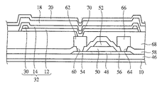
本実施形態による表示装置は、第2実施形態による表示装置と同様の有機エレクトロルミネッセンス素子とともに、スイッチング素子として薄膜トランジスタが設けられており、この薄膜トランジスタにより有機エレクトロルミネッセンス素子に印加する駆動電圧を制御するアクティブマトリクス型の表示装置である。以下、本実施形態による表示装置の構造について図10を用いて説明する。なお、図10は1画素分の構造を示したものであるが、実際には複数の画素がマトリクス状に配置されている。
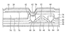
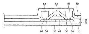
ガラス基板よりなる絶縁性基板10上には、シリコン酸化膜よりなるバッファ層46が形成されている。バッファ層46上には、ポリシリコン膜よりなるチャネル層48が形成されている。チャネル層48上には、シリコン酸化膜よりなるゲート絶縁膜50を介してゲート電極52が形成されている。ゲート電極52の両側のチャネル層48には、ソース領域54及びドレイン領域56が、それぞれ形成されている。こうして、絶縁性基板10上には、ゲート電極52、チャネル層48に形成されたソース領域54及びドレイン領域56を有し、有機エレクトロルミネッセンス素子に印加する駆動電圧を制御する薄膜トランジスタが形成されている。
薄膜トランジスタが形成された絶縁性基板10上には、層間絶縁膜58が形成されている。層間絶縁膜58上には、コンタクトホール60を介してソース領域54に接続されたソース電極62と、コンタクトホール64を介してドレイン領域56に接続されたドレイン電極66とがそれぞれ形成されている。
ソース電極62及びドレイン電極66が形成された層間絶縁膜58上には、層間絶縁膜68が形成されている。層間絶縁膜68には、ソース電極62に達するコンタクトホール70が形成されている。
コンタクトホール70が形成された層間絶縁膜68上には、コンタクトホール70を含む領域に、光反射性を有するAl膜よりなる光反射膜12が形成されている。光反射膜12の周縁部上には、光反射性を有するMo膜よりなる介在膜30が形成されている。周縁部上に介在膜30が形成された光反射膜12上には、光透過性を有するITO膜よりなる透明導電膜14が形成されている。介在膜30は光反射膜12及び透明導電膜14のそれぞれに電気的に接続するものであり、介在膜30により、透明導電膜14と光反射膜12との電気的接続が改善され、両者の間の導通が確保されている。こうして、層間絶縁膜68上に、光反射膜12と、透明導電膜14と、両者の間の導通を確保するための介在膜30とを有するアノード電極32が形成されている。アノード電極32は、層間絶縁膜68に形成されたコンタクトホール70を介して、薄膜トランジスタのソース電極62に電気的に接続されている。
アノード電極32上には、正孔注入層と、正孔輸送層と、発光層と、電子輸送層と、電子注入層とが順次積層されてなる有機エレクトロルミネッセンス層18が形成されている。有機エレクトロルミネッセンス層18上には、光透過性を有するAl/ITO積層膜よりなるカソード電極20が形成されている。こうして、層間絶縁膜68上に、アノード電極32と、有機エレクトロルミネッセンス層18と、カソード電極20とを有する有機エレクトロルミネッセンス素子が形成されている。
本実施形態による表示装置は、光反射膜12の存在により、絶縁性基板10とは反対側のカソード電極20側から光が取り出されるトップエミッション型となっている。したがって、絶縁性基板10上に形成された薄膜トランジスタにより発光面積が制限されることはなく、高い発光効率を実現することができる。
このようなトップエミッション型の本実施形態による表示装置に対して、図11に示す表示装置は、有機エレクトロルミネッセンス素子をともにスイッチング素子として薄膜トランスタを用いたボトムエミッション型の表示装置である。なお、図11は1画素分の構造を示したものであるが、実際には複数の画素がマトリクス状に配置されている。
図11に示すように、ガラス基板よりなる絶縁性基板100上には、バッファ層108が形成されている。バッファ層108上には、チャネル層110が形成されている。チャネル層110上には、ゲート絶縁膜112を介してゲート電極114が形成されている。ゲート電極114の両側のチャネル層110には、ソース領域116及びドレイン領域118が、それぞれ形成されている。こうして、絶縁性基板100上には、ゲート電極114、チャネル層110に形成されたソース領域116及びドレイン領域118を有する薄膜トランジスタが形成されている。
薄膜トランジスタが形成された絶縁性基板100上には、層間絶縁膜120が形成されている。層間絶縁膜120上には、コンタクトホール122を介してソース領域116に接続されたソース電極124と、コンタクトホール126を介してドレイン領域118に接続されたドレイン電極128とがそれぞれ形成されている。
ソース電極124及びドレイン電極128が形成された層間絶縁膜120上には、層間絶縁膜130が形成されている。層間絶縁膜130には、ソース電極124に達するコンタクトホール132が形成されている。
コンタクトホール132が形成された層間絶縁膜130上には、コンタクトホール132を含む領域に、ITO膜よりなる透明なアノード電極102と、有機エレクトロルミネッセンス層104と、Al膜やMg−Ag合金膜等よりなるカソード電極106とを有する有機エレクトロルミネッセンス素子が形成されている。アノード電極102は、層間絶縁膜130に形成されたコンタクトホール132を介して、薄膜トランジスタのソース電極124に電気的に接続されている。
図11に示すボトムエミッション型の表示装置では、有機エレクトロルミネッセンス層104において発生した光は、絶縁性基板100側から取り出される。このため、絶縁性基板10と有機エレクトロルミネッセンス素子との間に形成された薄膜トランジスタにより、有機エレクトロルミネッセンス素子の発光面積が制限され、本実施形態による表示装置のように高い発光効率を実現することは困難である。
また、本実施形態による表示装置は、第2実施形態による表示装置と同様の構造のアノード電極32を有するため、介在膜30により、Al膜よりなる光反射膜12とITO膜よりなる透明導電膜14との電気的接続が改善され、両者の間の導通が確保されている。これにより、薄膜トランジスタのソース電極62に電気的に接続された光反射膜12から正孔を有機エレクトロルミネッセンス層18に注入することができる。また、周縁部上に介在膜30が形成された光反射膜12を覆うように透明導電膜14が形成されているため、光反射膜12の腐食を防止することができる。また、駆動電圧印加時の発熱等により光反射膜12と透明導電膜14との間に生じるウィスカーによるアノード電極32とカソード電極20との間の短絡を防止することができる。また、有機エレクトロルミネッセンス層18には、従来の有機エレクトロルミネッセンス素子の有機エレクトロルミネッセンス層と同様の材料及び構造の有機エレクトロルミネッセンス層をそのまま用いることができる。
次に、本実施形態による表示装置の製造方法について図12及び図13を用いて説明する。
まず、ガラス基板よりなる絶縁性基板10上に、例えばCVD法により、例えば膜厚300nmのシリコン酸化膜よりなるバッファ層46を形成する。
次いで、バッファ層46上に、例えばCVD法により、例えば膜厚40nmのポリシリコン膜を形成する。なお、ポリシリコン膜の代わりにアモルファスシリコン膜を形成し、レーザアニール法等によりこれを結晶化してポリシリコン膜としてもよい。
次いで、フォトリソグラフィー及びドライエッチングにより、ポリシリコン膜をパターニングし、ポリシリコン膜よりなるチャネル層48を形成する(図12Aを参照)。
次いで、チャネル層48が形成されたバッファ層46上に、例えばCVD法により、例えば膜厚100nmのシリコン酸化膜を形成する。
次いで、例えばスパッタ法により、例えば膜厚300nmのAlNd(アルミニウム−ネオジム合金)膜を形成する。
次いで、フォトリソグラフィー及びドライエッチングにより、シリコン酸化膜及びAlNd膜をパターニングし、チャネル層48上に、シリコン酸化膜よりなるゲート絶縁膜50と、AlNd膜よりなるゲート電極52とを形成する。
次いで、ゲート電極52をマスクとして、例えばイオン注入法によりリンイオンをイオン注入し、ゲート電極52の両側のチャネル層48に、ソース領域54及びドレイン領域56をそれぞれ形成する。
こうして、絶縁性基板10上に、ゲート電極52、チャネル層48に形成されたソース領域54及びドレイン領域56を有する薄膜トランジスタを形成する(図12Bを参照)。
次いで、薄膜トランジスタが形成された絶縁性基板10上に、例えばCVD法により、例えば膜厚300nmのシリコン窒化膜よりなる層間絶縁膜58を形成する。
次いで、フォトリソグラフィー及びドライエッチングにより、層間絶縁膜58に、ソース領域54に達するコンタクトホール60及びドレイン領域56に達するコンタクトホール64をそれぞれ形成する(図12Cを参照)。
次いで、例えばスパッタ法により、コンタクトホール60、64が形成された形成された層間絶縁膜58上に、例えば膜厚100nm/100nm/100nmのTi(チタン)/Al/Ti膜を形成する。
次いで、フォトリソグラフィー及びドライエッチングにより、Ti/Al/Ti膜をパターニングし、Ti/Al/Ti膜よりなるソース電極62及びドレイン電極66をそれぞれ形成する(図13Aを参照)。
次いで、例えばCVD法により、ソース電極62及びドレイン電極66が形成された層間絶縁膜58上に、例えば膜厚3.0μmの感光性樹脂よりなる層間絶縁膜68を形成する。
次いで、リソグラフィーにより、層間絶縁膜68に、ソース電極62に達するコンタクトホール70を形成する(図13Bを参照)。
次いで、コンタクトホール70が形成された層間絶縁膜68上に、第2実施形態による表示装置の製造方法と同様にして、コンタクトホール70を介してソース電極62に接続するアノード電極32と、有機エレクトロルミネッセンス層18と、カソード電極20とを形成する(図13Cを参照)。
こうして、図10に示す本実施形態による表示装置が製造される。
このように、本実施形態によれば、有機エレクトロルミネッセンス素子を用いたアクティブマトリクス型の表示装置において、光反射性を有する光反射膜12と、光透過性を有する透明導電膜14とをアノード電極32が有するので、有機エレクトロルミネッセンス素子下に形成された薄膜トランジスタによる制限を受けずに、高い発光効率を有するトップエミッション型の表示装置を実現することができる。
また、光反射膜12が透明導電膜14により覆われているので、光反射膜12の腐食や、光反射膜12と透明導電膜14との間に生じるウィスカー等による素子特性の劣化を抑制することができる。
さらに、光反射膜12の周縁部上には、光反射膜12及び光反射膜12上に形成される透明導電膜14のそれぞれに電気的に接続し、両者の間の導通を確保するための介在膜30が形成されているため、薄膜トランジスタのソース電極62に電気的に接続された光反射膜12から正孔を有機エレクトロルミネッセンス層18に注入することができる。
また、有機エレクトロルミネッセンス層18は従来の有機エレクトロルミネッセンス素子と同様に透明導電膜14上に形成されるため、有機エレクトロルミネッセンス層18として、従来の有機エレクトロルミネッセンス素子と同様の材料及び構造の有機エレクトロルミネッセンス層をそのまま用いることができる。
なお、本実施形態においては、層間絶縁膜68上に、第2実施形態による表示装置と同様の有機エレクトロルミネッセンス素子が形成されていたが、第1又は第3実施形態による表示装置と同様の有機エレクトロルミネッセンス素子が形成されていてもよい。なお、第1実施形態による表示装置のように光反射膜12と透明導電膜14との間に介在膜30が形成されていない場合については、ソース電極62に達するコンタクトホール70内には光反射膜12を埋め込まない等の手段により、透明導電膜14がソース電極62に直接接続されているようにすることが望ましい。
また、第4実施形態による表示装置において絶縁性基板10の表面に滑らかな凹凸を形成した場合と同様に、層間絶縁膜68の表面に滑らかな凹凸を形成し、滑らかな凹凸が形成された層間絶縁膜68上に有機エレクトロルミネッセンス素子を形成してもよい。
(第6実施形態)
本発明の第6実施形態による表示装置について図14乃至図18を用いて説明する。図14は本実施形態による表示装置の構造を示す断面図、図15は本実施形態による表示装置の特性を示すグラフ、図16はアノード電極としてCr膜を用いた表示装置の構造を示す断面図、図17及び図18は本実施形態による表示装置の製造方法を示す工程断面図である。なお、図1、図3及び図4に示す第1実施形態による表示装置及びその製造方法と同様の構成要素については同一の符号を付し説明を省略し或いは簡略にする。
本実施形態による表示装置は、第1実施形態による表示装置と同様に、絶縁性基板上に形成された有機エレクトロルミネッセンス素子を有するパッシブマトリクス型の表示装置であり、その基本的構成は、第1実施形態による表示装置と同様である。本実施形態による表示装置は、光反射膜上に光透過性を有する絶縁層を介して透明導電膜よりなるアノード電極が形成されている点で、第1実施形態による表示装置と異なっている。
まず、本実施形態による表示装置の構造について図14を用いて説明する。なお、図14は1画素分の構造を示したものであるが、実際には複数の画素がマトリクス状に配置されている。
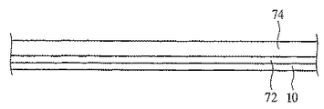
図14に示すように、ガラス基板よりなる絶縁性基板10上には、光反射性を有するAl膜よりなる光反射膜72が形成されている。光反射膜72は、所定の形状を有するものが画素毎に形成されていてもよいし、画素が配列された表示領域の全面に形成されていてもよい。
光反射膜72上には、光透過性を有する感光性樹脂よりなる絶縁層74が形成されている。絶縁層74の材料である感光性樹脂としては、例えばアクリル系樹脂が用いられている。絶縁層74は、光反射膜72の表面が剥き出しにならないように、光反射膜72を覆うように形成されている。
絶縁層74上には、光透過性を有するITOの透明導電膜よりなるアノード電極76が形成されている。アノード電極76上には、正孔注入層と、正孔輸送層と、発光層と、電子輸送層と、電子注入層とが順次積層されてなる有機エレクトロルミネッセンス層18が形成されている。有機エレクトロルミネッセンス層18上には、薄い膜厚で形成され光透過性を有するAl膜と、薄い膜厚で形成され光透過性を有するAg膜と、光透過性を有するITO膜よりなる透明導電膜とが順次積層されてなるカソード電極20が形成されている。こうして、絶縁性基板10上に、光反射膜72及び絶縁層74を介して、アノード電極76と、有機エレクトロルミネッセンス層18と、カソード電極20とを有する有機エレクトロルミネッセンス素子が形成されている。
本実施形態による表示装置では、カソード電極20から電子が有機エレクトロルミネッセンス層18に注入され、アノード電極76から正孔が有機エレクトロルミネッセンス層18に注入される。注入された電子は電子輸送層により発光層に輸送され、注入された正孔は正孔輸送層により発光層に輸送される。こうして発光層に輸送された電子と正孔とが、発光層において再結合することにより発光が生じる。発光層において発生した光は、アノード電極76側及びカソード電極20側に放出される。アノード電極76側に放出された光は、光透過性を有する絶縁層74を介して光反射膜72によりカソード電極20側に反射され、絶縁層74、アノード電極76、及び有機エレクトロルミネッセンス層18を介して、光透過性を有するカソード電極20側から取り出される。カソード電極20側に放出された光は、そのまま光透過性を有するカソード電極20側から取り出される。こうして、発光層において発生した光が、光透過性を有するカソード電極20側から取り出される。
このように、本実施形態による表示装置は、透明導電膜よりなるアノード電極76下に絶縁層74を介して形成された光反射膜72の存在により、絶縁性基板10とは反対側のカソード電極20側から光が取り出されるトップエミッション型となっている。したがって、第1実施形態による表示装置と同様に、絶縁性基板10と有機エレクトロルミネッセンス素子との間に他の素子が形成される場合において、他の素子が形成された領域からも光を取り出すことが可能となる。すなわち、有機エレクトロルミネッセンス素子の発光面積が他の素子により制限されることはなく、高い発光効率を実現することができる。
また、光反射膜72下に他の素子が形成される場合には、アノード電極76とカソード電極20とが重なる発光領域よりも幅広に光反射膜72を形成してもよい。このように光反射膜72を幅広に形成することで、有機エレクトロルミネッセンス素子の発光が他の素子の特性に影響するのを抑制することができる。
なお、アノード電極76と光反射膜72との間に形成する光透過性を有する絶縁層74の膜厚は、1μm以上に設定することが望ましい。これは、絶縁層74の膜厚を1μmよりも小さく設定すると、光の干渉の影響による減光が絶縁層74で起きてしまい、充分な発光効率を得ることができない虞があるためである。
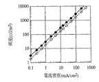
図15は、本実施形態による表示装置及び図16に示すCr膜よりなるアノード電極を用いた表示装置について、有機エレクトロルミネッセンス層に注入する電流密度を変えて輝度を測定し、両表示装置の特性を比較した結果を示すグラフである。図15に示すグラフの横軸は有機エレクトロルミネッセンス層に注入した電流密度を示し、縦軸は測定された表示装置の輝度を示している。また、図15に示すグラフにおいて、●印で示すプロットは本実施形態による表示装置についての測定結果を示し、○印で示すプロットは図16に示すCr膜よりなるアノード電極を用いた表示装置についての測定結果を示している。
本実施形態による表示装置では、光反射膜72として膜厚100nmのAl膜を、絶縁層74として膜厚3.0μmのアクリル系樹脂層を、アノード電極76として膜厚70nmのITO膜を用いた。また、有機エレクトロルミネッセンス層18として、膜厚140nmの2−TNATA膜よりなる正孔注入層と、膜厚10nmのα−NPD膜よりなる正孔輸送層と、少量のt(npa)pyをドープした膜厚30nmのAlq3膜よりなる発光層と、膜厚20nmのAlq3膜よりなる電子輸送層と、0.5nmのLiF膜よりなる電子注入層とが順次積層されてなるものを用いた。また、カソード電極20として、膜厚1.5nmのAl膜と、膜厚15nmのAg膜と、膜厚35nmのITO膜とが順次積層されてなるものを用いた。
本実施形態による表示装置と特性を比較した図16に示す表示装置は、アノード電極にCr膜を用いたトップエミッション型の表示装置である。図示するように、ガラス基板よりなる絶縁性基板100上には、Cr膜よりなるアノード電極134が形成されている。アノード電極134上には、有機エレクトロルミネッセンス層104が形成されている。有機エレクトロルミネッセンス層104上には、カソード電極106が形成されている。絶縁性基板100上にアノード電極134が直に形成されている点、及びアノード電極134にCr膜を用いた点を除いて、有機エレクトロルミネッセンス層104、カソード電極106の材料及び構造については、特性を比較した本実施形態による表示装置と同様した。
図15に示すグラフから明らかなように、同一の電流注入密度では、本実施形態による表示装置の方が、図16に示すアノード電極134にCr膜を用いた表示装置の場合の2倍程度の輝度が得られている。したがって、透明導電膜よりなるアノード電極76下に光透過性を有する絶縁層74を介して光反射膜72が形成された本実施形態による表示装置によれば、単にアノード電極にCr膜を用いる場合と比較して、効果的に発光効率を向上することができるといえる。
また、第1実施形態による表示装置と同様に、本実施形態による表示装置では、有機エレクトロルミネッセンス層18は、従来の有機エレクトロルミネッセンス素子と同様に、透明導電膜よりなるアノード電極76上に形成されている。このため、有機エレクトロルミネッセンス層18として、従来の有機エレクトロルミネッセンス素子と同様の材料及び構造の有機エレクトロルミネッセンス層をそのまま用いて高い発光効率を有するトップエミッション型の表示装置を構成することができる。
また、本実施形態による表示装置は、透明導電膜よりなるアノード電極76とAl膜よりなる光反射膜72との間には絶縁層74が介在し、光反射膜72は、その表面が剥き出しにならないように、絶縁層74により覆われている。したがって、第1実施形態による表示装置と同様に、製造工程におけるITO膜をパターニングする際に、Al膜よりなる光反射膜72の電池効果による腐食を防止することができる。
さらに、Al膜よりなる光反射膜72と透明導電膜よりなるアノード電極76との間には、絶縁層74が形成されている。このため、Al膜上にITO膜が直接形成されたアノード電極を用いた場合のように、有機エレクトロルミネッセンス素子に対する駆動電圧の印加時の発熱等により電極間の短絡の原因となるウィスカーが発生することはない。
次に、本実施形態による表示装置の製造方法について図17及び図18を用いて説明する。
まず、ガラス基板よりなる絶縁性基板10上に、例えばスパッタ法により、例えば膜厚150nmのAl膜を形成する。必要に応じて、フォトリソグラフィー及びエッチングにより、Al膜を画素毎に所定の形状にパターニングしてもよい。或いは、画素が配列される表示領域となる絶縁性基板10の全面に、Al膜を残存させてもよい。こうして、絶縁性基板10上に、Al膜よりなる光反射膜72を形成する(図17Aを参照)。
次いで、光反射膜72上に、例えばスピンコート法により、例えばアクリル系の感光性樹脂を塗布する。続いて、塗布された感光性樹脂を所定のマスクを用いて露光した後、所定の現像液を用いて露光された感光性樹脂を現像する。こうして、フォトリソグラフィーにより、例えば膜厚3.0μmの感光性樹脂よりなる絶縁層74を形成する(図17Bを参照)。ここで、絶縁層74は、光反射膜72の表面が剥き出しにならないように、光反射膜72を覆うように形成する。
本実施形態では、感光性樹脂により絶縁層74を形成しているため、平坦性の高い表面を有する絶縁層74を得ることができ、平坦性の高い表面上に、有機エレクトロルミネッセンス素子を形成することができる。
次いで、絶縁層74上に、例えばスパッタ法により、例えば膜厚70nmのITO膜78を形成する(図17Cを参照)。
次いで、フォトリソグラフィー及びエッチングにより、ITO膜78を所定の形状にパターニングする。こうして、絶縁層74上に、ITO膜78よりなるアノード電極76を形成する(図18Aを参照)。ITO膜78をパターニングする間、Al膜よりなる光反射膜72は絶縁層74により覆われ、その表面が露出することはない。したがって、電池効果による光反射膜72の腐食を防止することができる。
次いで、アノード電極76が形成された絶縁層74上に、例えば真空蒸着法により、所定の大きさに開口された蒸着マスクを介して、例えば膜厚140nmの2−TNATA膜と、例えば膜厚10nmのα−NPD膜と、例えば少量のt(npa)pyをドープした例えば膜厚30nmのAlq3膜と、例えば膜厚20nmのAlq3膜と、例えば0.5nmのLiF膜とを順次形成する。
こうして、アノード電極76上に、2−TNATA膜よりなる正孔注入層と、α−NPD膜よりなる正孔輸送層と、t(npa)pyをドープしたAlq3膜よりなる発光層と、Alq3膜よりなる電子輸送層と、LiF膜よりなる電子注入層とを有する有機エレクトロルミネッセンス層18を形成する(図18Bを参照)。
次いで、有機エレクトロルミネッセンス層18上に、例えば真空蒸着法及びスパッタ法により、所定の形状に開口されたマスクを介して、例えば膜厚1.5nmのAl膜と、例えば膜厚15nmのAg膜と、例えば膜厚35nmのITO膜とを順次形成し、Al/Ag/ITO積層膜を形成する。
こうして、Al/Ag/ITO積層膜よりなるカソード電極20を形成する(図18Cを参照)。
こうして、図14に示す表示装置が製造される。
このように、本実施形態によれば、有機エレクトロルミネッセンス素子を用いた表示装置において、透明導電膜よりなるアノード電極76下に、光透過性を有する絶縁層74を介して光反射性を有する光反射膜72が形成されているので、高い発光効率を有するトップエミッション型の表示装置を実現することができる。
また、光反射膜72が絶縁層74により覆われているので、光反射膜72の腐食等による素子特性の劣化を抑制することができる。
また、有機エレクトロルミネッセンス層18は従来の有機エレクトロルミネッセンス素子と同様に透明導電膜よりなるアノード電極76上に形成されるため、有機エレクトロルミネッセンス層18として、従来の有機エレクトロルミネッセンス素子と同様の材料及び構造の有機エレクトロルミネッセンス層をそのまま用いることができる。
なお、本実施形態による表示装置についても、第3実施形態による表示装置の場合と同様に、同一画素内に光反射膜72が形成された領域と光反射膜72が形成されていない領域とを設ける、すなわちアノード電極76とカソード電極20とが重なる発光領域に光反射膜72を部分的に形成することにより、上面発光型の領域と両面発光型の領域とを同一画素内に設けてもよい。
また、第4実施形態による表示装置の場合と同様に、絶縁性基板10の表面に滑らかな凹凸を形成し、滑らかな凹凸が形成された絶縁性基板10上に、光反射膜72、絶縁層74、及び有機エレクトロルミネッセンス素子を形成してもよい。または、絶縁層74の表面に滑らかな凹凸を形成し、滑らかな凹凸が形成された絶縁層74上に、有機エレクトロルミネッセンス素子を形成してもよい。絶縁性基板10又は絶縁層74の表面に形成された滑らかな凹凸により、第4実施形態による表示装置と同様に、アノード電極76、有機エレクトロルミネッセンス層18、及びカソード電極20の面積が、凹凸が形成されていない平坦な表面の絶縁性基板10上に形成される場合と比較して大きくなり、更に発光効率を向上することができる。
(第7実施形態)
本発明の第7実施形態による表示装置について図19乃至図22を用いて説明する。図19は本実施形態による表示装置の構造を示す断面図、図20乃至図22は本実施形態による表示装置の製造方法を示す工程断面図である。なお、図10、図12乃至図14、図17、及び図18に示す第5及び第6実施形態による表示装置及びその製造方法と同様の構成要素については同一の符号を付し説明を省略し或いは簡略にする。
本実施形態による表示装置は、第6実施形態による表示装置と同様の有機エレクトロルミネッセンス素子とともに、第5実施形態による表示装置と同様にスイッチング素子として薄膜トランジスタが設けられており、この薄膜トランジスタにより有機エレクトロルミネッセンス素子に印加する駆動電圧を制御するアクティブマトリクス型の表示装置である。以下、本実施形態による表示装置の構造について図19を用いて説明する。なお、図19は1画素分の構造を示したものであるが、実際には複数の画素がマトリクス状に配置されている。
ガラス基板よりなる絶縁性基板10上には、第5実施形態による表示装置と同様に、シリコン酸化膜よりなるバッファ層46を介して、ゲート電極52、チャネル層48に形成されたソース領域54及びドレイン領域56を有し、有機エレクトロルミネッセンス素子に印加する駆動電圧を制御する薄膜トランジスタが形成されている。
薄膜トランジスタが形成された絶縁性基板10上には、層間絶縁膜58が形成されている。層間絶縁膜58上には、コンタクトホール60を介してソース領域54に接続されたソース電極62と、コンタクトホール64を介してドレイン領域56に接続されたドレイン電極66とがそれぞれ形成されている。
ソース電極62及びドレイン電極66が形成された層間絶縁膜58上には、層間絶縁膜80が形成されている。
層間絶縁膜80上には、光反射性を有するAl膜よりなる光反射膜72が形成されている。光反射膜72には、層間絶縁膜80の薄膜トランジスタ上の領域を露出する開口部82が形成されている。なお、光反射膜72に形成された開口部82は、必ずしも層間絶縁膜80の薄膜トランジスタが形成された領域を露出するものである必要はなく、少なくとも層間絶縁膜80のソース電極62上の領域を露出するものであればよい。このような開口部82が形成された光反射膜72は、所定の形状を有するものが画素毎に形成されていてもよいし、画素が配列された表示領域の全面に形成されていてもよい。
光反射膜72及び開口部82から露出した層間絶縁膜80上には、光透過性を有する感光性樹脂よりなる絶縁層74が形成されている。絶縁層74の材料である感光性樹脂としては、例えばアクリル系樹脂が用いられている。絶縁層74は、光反射膜72の表面が剥き出しにならないように、光反射膜72を覆うように形成されている。
絶縁層74及び層間絶縁膜80には、ソース電極62に達するコンタクトホール70が形成されている。
コンタクトホール70が形成された絶縁層74上には、コンタクトホール70を含む領域に、光透過性を有するITOの透明導電膜よりなるアノード電極76が形成されている。アノード電極76は、絶縁層74及び層間絶縁膜80に形成されたコンタクトホール70を介して、薄膜トランジスタのソース電極62に電気的に接続されている。
アノード電極76上には、正孔注入層と、正孔輸送層と、発光層と、電子輸送層と、電子注入層とが順次積層されてなる有機エレクトロルミネッセンス層18が形成されている。有機エレクトロルミネッセンス層18上には、薄い膜厚で形成され光透過性を有するAl膜と、薄い膜厚で形成され光透過性を有するAg膜と、光透過性を有するITO膜よりなる透明導電膜とが順次積層されてなるカソード電極20が形成されている。こうして、光反射膜72上に絶縁層74を介して、アノード電極76と、有機エレクトロルミネッセンス層18と、カソード電極20とを有する有機エレクトロルミネッセンス素子が形成されている。
本実施形態による表示装置は、透明導電膜よりなるアノード電極76下に光透過性を有する絶縁層74を介して形成された光反射膜72の存在により、絶縁性基板10とは反対側のカソード電極20側から光が取り出されるトップエミッション型となっている。したがって、絶縁性基板10上に形成された薄膜トランジスタにより発光面積が制限されることはなく、高い発光効率を実現することができる。
また、本実施形態による表示装置では、光反射膜72に少なくとも層間絶縁膜80のソース電極62上の領域を露出する開口部82が形成され、透明導電膜よりなるアノード電極76がコンタクトホール70を介してソース電極62に直に電気的に接続されている。これにより、アノード電極76との電気的接続を確保することが困難な導電膜を介さずに、薄膜トランジスタのソース電極62に電気的に接続された光反射膜72から正孔を有機エレクトロルミネッセンス層18に注入することができる。また、光反射膜72を覆うように絶縁層74が形成されているため、光反射膜72の腐食を防止することができる。また、有機エレクトロルミネッセンス層18には、従来の有機エレクトロルミネッセンス素子の有機エレクトロルミネッセンス層と同様の材料及び構造の有機エレクトロルミネッセンス層をそのまま用いることができる。
なお、画素毎に所定の形状を有する光反射膜72を画素毎に形成する場合には、アノード電極76とカソード電極20とが重なる発光領域よりも幅広に光反射膜72を形成することが望ましい。このように光反射膜72を幅広に形成することで、有機エレクトロルミネッセンス素子の発光が薄膜トランジスタの特性に影響するのを抑制することができる。
次に、本実施形態による表示装置の製造方法について図20乃至図22を用いて説明する。
まず、図12A乃至図12C及び図13Aに示す第5実施形態による表示装置の製造方法と同様にして、絶縁性基板10上に、薄膜トランジスタ、ソース電極62及びドレイン電極66までを形成する(図20Aを参照)。
次いで、例えばCVD法により、ソース電極62及びドレイン電極66が形成された層間絶縁膜58上に、例えば膜厚300nmのシリコン酸化膜よりなる層間絶縁膜80を形成する(図20Bを参照)。なお、層間絶縁膜80には、シリコン酸化膜のほか、シリコン窒化膜等の無機絶縁膜、樹脂よりなる絶縁膜を用いることができる。
次いで、層間絶縁膜80上に、例えばスパッタ法により、例えば膜厚150nmのAl膜84を形成する。
次いで、リソグラフィーにより、Al膜84を所定の形状にパターニングし、Al膜84に、少なくとも層間絶縁膜80のソース電極62上の領域を露出する開口部82を形成する。Al膜84は、画素毎に所定の形状を有するようにパターニングしてもよいし、画素が配列される表示領域の全面に残存させてもよい。こうして、Al膜84よりなる光反射膜72を形成する(図21Aを参照)。なお、図21Aでは、層間絶縁膜80の薄膜トランジスタ上の領域を露出する開口部82を光反射膜72に形成した場合について示している。
次いで、光反射膜72及び開口部82から露出する層間絶縁膜80上に、例えばスピンコート法により感光性樹脂を塗布し、感光性樹脂層86を形成する(図21Bを参照)。
感光性樹脂層86を所定のマスクを用いて露光した後、所定の現像液を用いて露光された感光性樹脂層86を現像し、層間絶縁膜80のソース電極62上の領域を露出する開口部88を感光性樹脂層86に形成する。こうして、フォトリソグラフィーにより、開口部88が形成された光透過性を有する感光性樹脂層86よりなる絶縁層74を形成する(図21Cを参照)。ここで、絶縁層74は、光反射膜72の表面が剥き出しにならないように、光反射膜72を覆うように形成する。
次いで、例えばドライエッチングにより、開口部88が形成された絶縁層74をマスクとして、層間絶縁膜80に、ソース電極62に達する開口部90を形成する。
こうして、層間絶縁膜80に形成された開口部90と、絶縁層74に形成された開口部88とが接続してなるコンタクトホール70を形成する(図22Aを参照)。なお、コンタクトホール70には光反射膜72が露出しないように、光反射膜72の開口部82の大きさ、絶縁層74の開口部88の大きさ、エッチング条件等を予め適宜設定しておくことが望ましい。これは、次のような理由による。すなわち、コンタクトホール70に光反射膜72が露出すると、この後に形成するアノード電極76と光反射膜72とが接触し、両者の間に寄生容量が形成されてしまうので、このような寄生容量による素子特性の劣化を回避するためである。
このように、本実施形態による表示装置の製造方法では、絶縁層74を感光性樹脂により形成し、層間絶縁膜80をエッチングする際のマスクとしても絶縁層74を用いるので、少ない工程数でコンタクトホール70までを形成することができる。なお、絶縁層74としてシリコン酸化膜等の光透過性を有する無機絶縁膜を用いることもできる。この場合、無機絶縁膜よりなる絶縁層74を形成する工程に加えて、絶縁層74及び層間絶縁膜80にコンタクトホール70を形成するためのエッチングマスクとして用いるレジスト膜を形成する工程、レジスト膜を除去する工程も必要となる。このため、感光性樹脂により絶縁層74を形成する場合と比較して工程数が多くなる。
次いで、コンタクトホール70が形成された絶縁膜74上に、第6実施形態による表示装置の製造方法と同様にして、コンタクトホール70を介してソース電極62に接続するアノード電極76と、有機エレクトロルミネッセンス層18と、カソード電極20とを形成する(図22Bを参照)。
こうして、図19に示す本実施形態による表示装置が製造される。
このように、本実施形態によれば、有機エレクトロルミネッセンス素子を用いた表示装置において、透明導電膜よりなるアノード電極76下に、光透過性を有する絶縁層74を介して光反射性を有する光反射膜72が形成されているので、有機エレクトロルミネッセンス素子下に形成された薄膜トランジスタによる制限を受けずに、高い発光効率を有するトップエミッション型の表示装置を実現することができる。
また、光反射膜72が絶縁層74により覆われているので、光反射膜72の腐食等による素子特性の劣化を抑制することができる。
さらに、有機エレクトロルミネッセンス層18は従来の有機エレクトロルミネッセンス素子と同様に透明導電膜よりなるアノード電極76上に形成されるため、有機エレクトロルミネッセンス層18として、従来の有機エレクトロルミネッセンス素子と同様の材料及び構造の有機エレクトロルミネッセンス層をそのまま用いることができる。
(変形実施形態)
本発明は上記実施形態に限らず種々の変形が可能である。
例えば、上記実施形態では、絶縁性基板10としてガラス基板を用いる場合について説明したが、絶縁性基板10はガラス基板に限定されるものではない。例えば、ポリカーボネート、ポリエチレンテレフタレート等の樹脂フィルムを絶縁性基板10として用いてもよい。樹脂フィルムを絶縁性基板10として用いることにより、可撓性を有するフレキシブルな表示装置を実現することができる。また、トップエミッション型の表示装置のみを構成する場合にあっては、絶縁性基板10は必ずしもガラス基板等のように光透過性を有するものである必要はない。但し、第3実施形態による表示装置の場合のように、同一基板上に上面発光部40と両面発光部44とを設ける場合にあっては、光透過性を有する基板を絶縁性基板10として用いる必要がある。
また、上記実施形態では、光反射膜12の周縁部上に介在膜30が形成されている場合について説明したが、介在膜30は必ずしも光反射膜12の周縁部上に形成されている必要はなく、光反射膜12の所定の領域上に部分的に形成されていればよい。
また、上記実施形態では、有機エレクトロルミネンセンス層18の発光層において発生した光をカソード電極20側へ反射するための光反射膜12、72としてAl膜を用いる場合について説明したが、光反射膜12、72はAl膜に限定されるものではない。光反射膜12、72としては、Al又はAlを主成分とする合金のほか、例えば、Ag、Nd(ネオジム)、Si(シリコン)、Ti、W(タングステン)、Cu(銅)、Nb(ニオブ)、Ta(タンタル)、C(炭素)、又は少なくともこれらのうちのいずれかを主成分とする合金よりなる光反射性を有する導電膜を用いることができる。
また、上記実施形態では、Al膜よりなる光反射膜12とITO膜よりなる透明導電膜14との電気的接続を改善し、両者の間の導通を確保するための介在膜30としてMo膜を用いる場合について説明したが、介在膜30はMo膜に限定されるものではない。介在膜30としては、Mo又はMoを主成分とする合金のほか、例えば、W、Ta、Ti、Cr、又は少なくともこれらのうちのいずれかを主成分とする合金等の高融点金属よりなる導電膜を用いることができる。
また、上記実施形態では、光反射膜12上に形成する透明導電膜14、アノード電極76としてITO膜を用いる場合について説明したが、透明導電膜14、アノード電極76はITO膜に限定されるものではない。透明導電膜14としては、ITO膜のほか、例えば、IZO(亜鉛をドープした酸化インジウム)膜、ZnO(酸化亜鉛)膜等の光透過性を有する導電膜を用いることができる。
また、上記実施形態では、有機エレクトロルミネッセンス層18として、2−TNATA膜よりなる正孔注入層と、α−NPD膜よりなる正孔輸送層と、t(npa)pyをドープしたAlq3膜よりなる発光層と、Alq3膜よりなる電子輸送層と、LiF膜よりなる電子注入層とが順次積層されてなるものを用いる場合について説明したが、有機エレクトロルミネッセンス層18の構造及び材料は、これに限定されるものではない。有機エレクトロルミネッセンス層18の構造には、発光層のみの単層構造、正孔輸送層と発光層または発光層と電子輸送層の2層構造、正孔輸送層と発光層と電子輸送層との3層構造を適用することができる。また、有機エレクトロルミネッセンス層18を構成する正孔注入層、正孔輸送層、発光層と、電子輸送層、電子注入層の材料には、あらゆる有機エレクトロルミネッセンス材料を用いることができる。
また、上記実施形態では、カソード電極20としてAl/ITO積層膜、Al/Ag/ITO積層膜を用いる場合について説明したが、カソード電極20はAl/ITO積層膜、Al/Ag/ITO積層膜に限定されるものではない。カソード電極20としては、Al/ITO積層膜、Al/Ag/ITO積層膜のほか、例えば、ITO単膜、IZO膜、ZnO膜、Al単膜、Ag単膜又はこれらの積層膜等の光透過性を有する導電膜を用いることができる。なお、Al膜、Ag膜等をカソード電極20として用いる場合には、光透過性を有するように、これらの膜を薄く形成する必要がある。
また、上記実施形態では、絶縁層74として感光性樹脂よりなるものを用いる場合について説明したが、絶縁層74は、光透過性を有するものであれば、感光性樹脂よりなるものに限定されるものではない。絶縁層74としては、感光性樹脂よりなるものほか、シリコン酸化膜、シリコン窒化膜、シリコン窒化酸化膜等の光透過性を有する無機絶縁膜を用いることができる。また、絶縁層74は、光透過性を有するものであれば無色である必要はなく、絶縁層74として、ポリイミド等の有色樹脂よりなるものを用いることもできる。
また、上記実施形態では、薄膜トランジスタとしてトップゲート型のものを用いる場合について説明したが、薄膜トランジスタとしてはボトムゲート型のものを用いてもよい。また、チャネル層48にポリシリコン膜を用いる場合について説明したが、チャネル層48にはアモルファスシリコン膜を用いてもよい。
また、上記実施形態では、スイッチング素子として薄膜トランジスタを用いる場合について説明したが、他のスイッチング素子を用いてもよい。例えば、二端子素子であるダイオードを利用したMIM(金属−絶縁膜−金属)構造のスイッチング素子を用いてもよい。