JP5116203B2 - Vacuum plasma processor and coil - Google Patents
Vacuum plasma processor and coil Download PDFInfo
- Publication number
- JP5116203B2 JP5116203B2 JP2002507035A JP2002507035A JP5116203B2 JP 5116203 B2 JP5116203 B2 JP 5116203B2 JP 2002507035 A JP2002507035 A JP 2002507035A JP 2002507035 A JP2002507035 A JP 2002507035A JP 5116203 B2 JP5116203 B2 JP 5116203B2
- Authority
- JP
- Japan
- Prior art keywords
- coil
- windings
- winding
- sections
- common center
- Prior art date
- Legal status (The legal status is an assumption and is not a legal conclusion. Google has not performed a legal analysis and makes no representation as to the accuracy of the status listed.)
- Expired - Fee Related
Links
- 238000004804 winding Methods 0.000 claims description 119
- 230000005284 excitation Effects 0.000 claims description 21
- 238000000034 method Methods 0.000 claims description 12
- 230000008569 process Effects 0.000 claims description 6
- 206010026749 Mania Diseases 0.000 claims 2
- 235000012431 wafers Nutrition 0.000 description 74
- 230000002093 peripheral effect Effects 0.000 description 25
- 230000004907 flux Effects 0.000 description 23
- 239000002184 metal Substances 0.000 description 10
- 229910052751 metal Inorganic materials 0.000 description 10
- 239000004065 semiconductor Substances 0.000 description 8
- 239000003990 capacitor Substances 0.000 description 7
- 238000009826 distribution Methods 0.000 description 7
- 238000005530 etching Methods 0.000 description 7
- 239000000463 material Substances 0.000 description 5
- 230000008878 coupling Effects 0.000 description 4
- 238000010168 coupling process Methods 0.000 description 4
- 238000005859 coupling reaction Methods 0.000 description 4
- 230000000694 effects Effects 0.000 description 4
- 230000005672 electromagnetic field Effects 0.000 description 4
- 230000005540 biological transmission Effects 0.000 description 3
- RYGMFSIKBFXOCR-UHFFFAOYSA-N Copper Chemical compound [Cu] RYGMFSIKBFXOCR-UHFFFAOYSA-N 0.000 description 2
- 229910052802 copper Inorganic materials 0.000 description 2
- 239000010949 copper Substances 0.000 description 2
- 238000009792 diffusion process Methods 0.000 description 2
- 230000006872 improvement Effects 0.000 description 2
- 150000002500 ions Chemical class 0.000 description 2
- 239000002245 particle Substances 0.000 description 2
- 230000004044 response Effects 0.000 description 2
- 239000000758 substrate Substances 0.000 description 2
- 238000012935 Averaging Methods 0.000 description 1
- 238000010521 absorption reaction Methods 0.000 description 1
- 230000002411 adverse Effects 0.000 description 1
- 230000008859 change Effects 0.000 description 1
- 238000010276 construction Methods 0.000 description 1
- 238000000151 deposition Methods 0.000 description 1
- 238000010586 diagram Methods 0.000 description 1
- 239000003989 dielectric material Substances 0.000 description 1
- 239000011521 glass Substances 0.000 description 1
- 238000004519 manufacturing process Methods 0.000 description 1
- 230000007246 mechanism Effects 0.000 description 1
- NJPPVKZQTLUDBO-UHFFFAOYSA-N novaluron Chemical compound C1=C(Cl)C(OC(F)(F)C(OC(F)(F)F)F)=CC=C1NC(=O)NC(=O)C1=C(F)C=CC=C1F NJPPVKZQTLUDBO-UHFFFAOYSA-N 0.000 description 1
- 229910021420 polycrystalline silicon Inorganic materials 0.000 description 1
- 229920005591 polysilicon Polymers 0.000 description 1
- 239000010453 quartz Substances 0.000 description 1
- VYPSYNLAJGMNEJ-UHFFFAOYSA-N silicon dioxide Inorganic materials O=[Si]=O VYPSYNLAJGMNEJ-UHFFFAOYSA-N 0.000 description 1
- 239000007787 solid Substances 0.000 description 1
- 238000009423 ventilation Methods 0.000 description 1
Images


Classifications
-
- H—ELECTRICITY
- H01—ELECTRIC ELEMENTS
- H01J—ELECTRIC DISCHARGE TUBES OR DISCHARGE LAMPS
- H01J37/00—Discharge tubes with provision for introducing objects or material to be exposed to the discharge, e.g. for the purpose of examination or processing thereof
- H01J37/32—Gas-filled discharge tubes
- H01J37/32009—Arrangements for generation of plasma specially adapted for examination or treatment of objects, e.g. plasma sources
- H01J37/32082—Radio frequency generated discharge
- H01J37/321—Radio frequency generated discharge the radio frequency energy being inductively coupled to the plasma
- H01J37/3211—Antennas, e.g. particular shapes of coils
Description
(発明の分野)
本発明は概して、真空チェンバ内のガスをチェンバ内でワークピースを処理するプラズマへと励起するための、高周波応答コイルを有するプラズマプロセッサに関し、さらに特定すると実質的に対称および非対称の巻線を有する実質的に平板状のコイルを含むそのようなプロセッサ、およびそのようなコイルに関する。本発明のまた別の態様は、様々な直径を有する円形のワークピースをプラズマ処理する方法、さらに特定すると、様々な周縁の長さを有するワークピースを処理するときに、同じチェンバもしくは同じ幾何学形状を有する複数チェンバが様々な周縁寸法を有する高周波励起コイルに結合される方法に関する。
【0001】
(発明の背景)
ワークピースを真空チェンバにおいて高周波プラズマで処理するプロセッサの一タイプは高周波電源に応答するコイルを含む。このコイルは高周波電源に応答してチェンバ内のイオン化可能なガスを励起してプラズマにする電磁場を発生する。このコイルは、普通は処理される製品の平板状で水平に広がる表面に平行な方向に広がる誘電窓の上部に設置されるかまたはそれに隣接される。励起されたプラズマはチェンバ内のワークピースと相互作用してワークピースをエッチングするかまたはその上に物質を堆積させる。ワークピースは通常は平板状の円形表面を有する半導体ウェハもしくは固体誘電体プレート、例えばフラットパネル・ディスプレーに使用される長方形のガラス基板または金属プレートである。
【0002】
Ogleの米国特許第4,948,458号は上記の結果を達成するための多数回巻きの渦巻き状コイルを開示している。概してアルキメデス型であるこの渦巻きはインピーダンス整合ネットワークを介して高周波電源に接続された内側端子と外側端子との間を放射方向かつ円周方向に広がる。この一般的なタイプのコイルは磁性および容量性の場の成分を有する振動高周波場を生じ、それが誘電窓を通って伝播して窓近傍のチェンバ内のプラズマの一部のガス中の電子を加熱する。振動高周波場がプラズマ中で電流を誘導し、それがプラズマ中の電子を加熱する。窓近傍のプラズマ部分の磁場の空間分布はコイルの各々の巻線によって生じる個々の磁場成分の合計の関数である。各々の巻線によって生じる個々の磁場成分は各々の巻線の高周波電流の大きさの関数であり、それは高周波電源の周波数でのコイルの伝送線効果が理由となって様々な巻線で異なる。
【0003】
Ogleの4,948,458特許で開示され、それに基づく渦巻き設計では、渦巻き状コイルの高周波電流は窓近傍のプラズマ部分でトロイダル形状の磁場領域を発生するように分布し、ガスによってパワーが吸収され、ガスはプラズマに励起する。1.0から10mTorr程度の低圧では、リング形状の領域からのプラズマの拡散は、チェンバの中央および周縁部のワークピースのすぐ上部でプラズマ密度ピークを発生させ、そのため、ワークピースを処理するイオンと電子の複数のピーク密度はワークピース中心線およびワークピース周縁部に近接する。10から100mTorr程度の中間の圧力範囲では、プラズマ中の電子、イオンおよび中性子の気相衝突がプラズマ荷電粒子のトロイダル領域外への実質的な拡散を妨害する。結果として、ワークピースのリング状領域で比較的大きなプラズマ束が存在するが、中央および周縁のワークピース部分では小さなプラズマ束となる。
【0004】
これらの異なる動作条件はリングとリング内外の容積との間でプラズマ束(すなわちプラズマ密度)の大きなバラツキを生じる結果につながり、ワークピースに入射するプラズマ束の標準偏差が大きくなる。ワークピースに入射するプラズマ束の尺度はワークピースのオングストローム/分で表わされるエッチング速度であり、Ogleのタイプのコイルのエッチング速度均一性の標準偏差は通常は3.0%よりも大きい。ワークピースに入射するプラズマ束の標準偏差が大きいと、ワークピースは不均一に処理される傾向がある、すなわちワークピースの様々な部分が異なる量でエッチングされ、および/または異なる量の分子がそれらに堆積される傾向がある。
【0005】
プラズマの均一性を向上させるために数多くのコイルが設計されてきた。1998年6月2日に発布された同一出願人による米国特許第5,759,280号(Hollandら)は、商業的実施形態で12インチの直径を有し、かつ内壁の円の直径14.0インチを有する真空チェンバとの組み合わせで動作するコイルを開示している。このコイルは14.7インチの直径と0.8インチの均一な厚さを有する石英窓を介してチェンバ内部に電磁場を加える。各々のワークピースの中心は、コイルの中心線と一致するように直径200mmを有する円形半導体ウェハであるワークピースが窓の底面の4.7インチ下のワークピースホルダに配置される。
【0006】
5,759,280号特許のコイルは4,948,458号特許のコイルよりも、ワークピースにわたってかなり小さいプラズマ束のバラツキを発生させる。5ミリTorrで稼動しているチェンバにおいて、200mmのウェハ上の5,759,280号特許のコイルによって発生するプラズマ束から結果的に得られるエッチング速度均一性の標準偏差は約2.0%であり、同じ条件下で動作する4,948,458号特許のコイルの場合の標準偏差約3.0%よりもかなり改善されている。5,759,280号特許のコイルは、ワークピースの中央部のプラズマ密度が、ワークピース中間部分のプラズマ密度よりも大きくなる磁場を引き起こし、そのためにワークピース周辺部のプラズマ密度を超えることになる。5,759,280号特許のコイルでのチェンバの様々な部分のプラズマ密度のバラツキは、より低い標準偏差を生じ、同じ動作条件での4,948,458号特許のコイルのそれよりもはるかに小さい。
【0007】
300mmの直径を有する円形半導体ウェハの出現とともに、200mmと300mmの直径の円形半導体ウェハをプラズマ処理するのに同じ真空チェンバを使用することが提案されてきた。図1は両方の直径のウェハを処理するのに使用できるプロセッサの図面である。図1に描かれたタイプのプロセッサでは、同じプロセッサが両方の直径について、異なる時間に使用され、または同じ幾何学形状を備えた複数のチェンバを有するプロセッサが、200mmと300mmの直径のウェハを別々に処理するのに使用する。
【0008】
図1の真空プラズマワークピースプロセッサは、20インチの内径を有するグラウンド接地された金属壁12、金属の基台プレート14、および中心から周縁部まで同じ厚さを有し、かつ直径がチェンバ10の内径を超えることによって壁12の上部エッジを担う誘電窓構造19で構成される円形の上部プレート構造18を含む円筒の真空チェンバ10を含む。真空チェンバ10のシールは従来のガスケット(図示せず)によって供給される。図1のプロセッサは、通常は円形半導体ウェハ(すなわち基板)をエッチングするか、またはそのようなウェハ上に分子を堆積させるために使用される。
【0009】
プラズマ状態へと励起され得る適切なイオン化可能なガスが、窓19のポート20を介してガス源(図示せず)からチェンバ10の内部に供給される。チェンバ10の内部は、基台プレート14のポート22に接続された真空ポンプ(図示せず)によって1乃至100ミリTorrの範囲で変わり得る圧力で、真空状態に維持される。
【0010】
チェンバ内のガスは適切な電源によって励起され、Ogleの4,948,458号特許に開示されたコイルによって励起されるプラズマよりもかなり均一な密度を有するプラズマを供給する。この電源は正方形の断面と中空の内部を有する実質的に平坦な金属のコイル24を含み、コイル24は通常は正方形の銅チューブでできている。コイル24は窓19のすぐ上部に装着され、通常は13.56MHzの固定周波数を有し、かつ通常、固定の振幅エンベロープを有する高周波電源26によって励起される。コイル24内の電流は窓19の近傍でチェンバ10内に十分に大きい磁束を発生させ、チェンバ内のイオン化可能なガスをプラズマへと励起する。
【0011】
高周波電源26の出力端子とコイル24の励起端子との間に接続されたインピーダンス整合ネットワーク28は、高周波電源の出力をコイルに結合させる。インピーダンス整合ネットワーク28は、電源26とコイル24及びコイルが励起するプラズマ負荷を含めた負荷との間のインピーダンス整合を達成するために、コントローラ(図示せず)が知られている方式で変化させる可変リアクタンス(図示せず)を含む。
【0012】
200mmまたは300mmの直径の円形のワークピース32は、チェンバ10内で円形のワークピースホルダ(すなわちチャックもしくはプラテン)30の表面に固定して装着される。ワークピース32を担持するチャック30の表面は、窓19の表面と平行である。通常では静電タイプであるチャック30は、2つの異なる直径のうちの1つを有し、それはチェンバ10内で特定の時間に処理されるワークピースの直径に応じて決まる。ワークピース32はDC電源(図示せず)のDC電位をチャックの1つもしくは複数の電極(図示せず)に印加することによって、チャック30の表面に通常は静電的にクランプされる。
【0013】
高周波電源31は可変リアクタンス(図示せず)を含むインピーダンス整合ネットワーク33に一定の振幅エンベロープを有する高周波電圧を供給する。整合ネットワーク33は電源31の出力をチャック30の電極に結合させる。電源31のインピーダンスをチャック30の電極に結合された負荷インピーダンスに整合させるために、コントローラ(図示せず)が整合ネットワーク33の可変リアクタンスを制御する。電極に結合した負荷は本来はチェンバ10内のプラズマである。よく知られているように、電源31がチャック30の電極に印加する高周波電圧はプラズマ中の荷電粒子と相互作用してワークピース32にDCバイアスを発生させる。
【0014】
平板状のコイル24を取り囲み、上端プレート18の上部を延びているのは、中にコイルが収まる正方形断面を有する金属のチューブもしくはシールド34である。シールド34はコイル24に起源を発する電磁場を周囲の環境から切り離す。シールド34とコイル24の周縁領域との間の距離は十分にあり、コイル24の周縁領域によって生じる磁場がシールド34により有意に吸収されるのを防いでいる。
【0015】
コイル24の外径に対して円筒形状のチェンバ10の直径は、コイルの周縁領域において生じる磁場のチェンバ壁12による実質的な吸収を阻止するのに十分なほどに大きい。誘電窓構造19の直径は、チェンバ10の内径よりも大きく、チェンバ10の上面全体が誘電窓構造19で構成される程度まで可能である。
【0016】
ワークピース32の処理面と誘電窓構造19の底面の間の距離はワークピースの露出処理面に最も均一なプラズマ束を供給するように選択される。通常では、ワークピースの処理面と誘電窓の底の間の距離は、チェンバ10の直径の約0.3乃至0.4倍であり、チェンバ12の内径は20インチ、5,759,280号特許の先行技術の形状を有するコイル24の直径は、直径200mmのウェハについては13インチであり、シールド34は各々の側部で23.5インチの長さを有し、ワークピースの処理面と誘電窓の底の間の距離は6.0インチである。
【0017】
平板状のコイル24は伝送線として機能し、コイルの長さに沿った定在波パターンを生じる。定在波パターンはコイルの長さに沿った高周波電圧と電流の大きさのバラツキを結果的に示す。コイルによって生じる磁束のこれらの高周波電流の大きさに対する依存性は、コイルの様々な部分の支配下にあるチェンバ10内の様々な部分に発生するプラズマの量が異なる結果につながる。平板状コイル24の高周波電流の伝送線挙動は、中央コイル区画より発生する磁束の量と比べて、周縁コイル区画より発生する磁束の量を増大させる。この効果は最大高周波電流領域が周縁コイル区画となるように高周波でコイル24を励起することによって確立する。
【0018】
図2に描いたように、5,759,280号特許の形状を備えた平板状コイル24は、実質的に半円形の内側ループ40、42および実質的に円形周縁区画46と48および実質的に円形の中間区画44を含む。ループ40と42の各々は、コイル24のほぼ半周巻きを形成するのに対して、ループ44、46および48の各々は、ほぼ全周巻きを形成する。これらの全周および半周巻きは互いに直列に接続される。区画40、42、44、46および48のすべては、中心コイル軸50と同軸であり、ウェハがチャック30の定位置にクランプされると、今度はチェンバ10の中心軸およびウェハ32の中心と一致する。コイル24の中央部分にある対向する励起端子52と54は、リード58と56によって整合ネットワーク28経由で高周波電源26の対向する端子およびキャパシタ80の一方の電極(他方の電極はグラウンド接地される)にそれぞれ結合される。ループ40の端子52の反対側の端部にある端子60は、コイル24の平面のいくぶん上の領域に位置する金属のストラップ64によって、外側ループ区画48の端部端子66に接続される。隣接する区画40、42、44、46および48の間の間隔およびストラップ64とコイル24の残り部分との間隔は、それらの間のアークを十分に防止するほど大きい。区画40、42、44、46および48の外側エッジの半径はそれぞれ2インチ、2インチ、3.5インチ、5.5インチおよび6.5インチである。
【0019】
区画48は端子66から360°よりもわずかに小さいところに第2の端子68を有する。端子68はストラップ72を介してループ区画46の端子70に接続される。ほぼ360°の角度の広がりを有するループ46は、半径方向と円周方向に延びるストラップ78を介してループ44の端子76に接続される第2の端部端子74を有する。ほぼ360°の角度の広がりを有するループ44は、半径方向と円周方向に延びるストラップ82を介して区画42の端子54と反対側の端部にある端子62に接続される第2の端部端子80を有する。
【0020】
j=√(−1)、fが高周波電源26の周波数、Cがキャパシタ80のキャパシタンスである場合に容量性インピーダンスZcap=1/(j2πfC)を有するキャパシタ80は、位相をシフトをすることによってコイル24の全長にわたって電圧および電流分布の位置をシフトする。電圧および電流分布は、‘498号特許でOgleが開示するタイプのコイルの励起の結果として得られる束よりも、かなり均一なプラズマ束をワークピース32の処理面に供給する高周波電磁場を、コイルが発生させるようにコイル24内でシフトされる。
【0021】
コイル24の電圧と電流は、コイル端子54でのピークピーク高周波電流が最小でかつコイル端子52のピークピーク高周波電流と等しくなるようにキャパシタ80の値を選択することによって配分される。この条件で、コイルは端子52と54で対極性最大ピークピーク高周波電圧を有し、コイルの最大高周波電流は導電性ストラップ72の近傍で生じる。コイル内の高周波電圧および電流の分布は次のように概算することが可能であり、
Vpkpk (X)=V0 pkpkcos[β(x+xo)]および
Ipkpk (X)=I0 pkpksin[β(x+xo)]
ここで、
xはコイルの端子54から測定した直線距離、
βは高周波電源26の光速cで割り算をした角周波数、
xoはキャパシタ80の値によって決定されるゼロからのオフセット、
V0 pkpkおよびI0 pkpkはそれぞれコイルの最大高周波ピークピーク電圧および電流である。
【0022】
キャパシタ80の値はxoがコイルに流れる高周波電流の波長(λ=c/f)のおよそ0.15倍になるように選択される。
【0023】
コイル24の周縁領域はコイルの中央領域よりも大きな磁束を発生するが、その理由はピークピーク高周波電流の大きさがコイルの周縁区画で中央区画のピークピーク高周波電流の大きさと比較してさらに大きいからである。最大のピークピーク高周波電流の振幅は実質的に円形のループ区画46で生じる。隣接するループ区画44と48、およびループ区画46でのピークピーク高周波電流の振幅とループ区画44、46と48のお互いからの間隔は、これら3つのループ区画からの磁束が空間で混ざり合って窓19の直下で、比較的広い環状領域にわたって最大値を有する全磁束密度を与えるように設定する。環状領域はループ区画46と48の間から中間区画44と内側区画40と42の間まで広がる。
【0024】
コイルの様々な部分を流れる高周波電流の大きさのバラツキは空間で平均化され、Ogleの‘498号特許のコイルによって達成されるよりも均一なプラズマをウェハ32に入射させる補助になる。コイルの様々な部分のこれら様々な電流値の空間的平均化は、特にコイル周縁部付近のコイル区画の超高周波電流領域において、プラズマ密度の実質的な非放射状の非対称性を回避すると以前は考えられていた。全磁束もまた、角座標θの関数として、Ogleの特許のコイルでのケースよりもかなり一定している。
(ここでθはコイルの中心点50°を通って延びる基準角度に関して、コイル周辺部についての角度を表す、例えば図2では、基準角度は中心点50の左側へ水平に延びる)。
【0025】
特定の座標値θに沿って一定で空間的に平均化した磁束は、Ogleの‘498号特許に開示されたコイルから結果的に得られるプラズマよりも、θに沿って放射状でさらに対称性を帯びたプラズマを供給する。2つの実質的に半円形で等しい半径の区画40と42のピークピーク高周波電流の振幅は、その他の区画の電流の振幅よりも有意に小さい。区画40と42は十分な磁束を誘導し、それらはその他の区画44、46および48から誘導された磁束と空間的に平均化され、それによりチェンバの直径を横切ってワークピース32の処理面の高さで発生するプラズマ束は、Ogleの特許のコイルで達成されるよりもかなり均一になる。
【0026】
平板状コイル24の様々な部分(例えば、同じ角座標位置θのループ区画46と48の部分間)の電圧をプラズマに静電的(すなわち容量性)に結合することは発生するプラズマ束の均一性に影響する。プラズマへのこれらの電圧の容量性結合は、コイルの区画で発生するピークピーク電圧の大きさ、ならびにコイルをプラズマから隔てる窓19の厚さと誘電体材料によって決まる。高周波電圧によって発生する容量性の電流の影響は、端子52と54で最大の高周波ピークピーク電圧を生じさせることによって最小限にされる。コイル24の幾何学形状およびキャパシタ80の値の選択が、端子52と54で最大の高周波ピークピーク電圧を生じさせる。平板状コイル24を高周波励起することは、ワークピース32全体にわたってOgleの4,948,458号特許のコイルから結果的に得られるよりもかなり均一な束を有する実質的に平板状のプラズマを発生させる。
【0027】
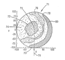
集積回路の形体が小さくなればなるほど、図2と関連して説明したコイルによって発生する200mmのウェハに入射するプラズマの均一性が頻繁に不十分となることが判明した。説明した13インチ直径のコイルでプラズマが励起されるとき、200mmウェハ上に非対称直径のプラズマ束分布が図1のプロセッサで形成される。この非対称性は200mm半導体ウェハに形成される0.18マイクロメートルの形体を有する半導体デバイスに多大な悪影響を及ぼす。特に、13.56MHzの高周波電源26に接続された図2のコイルによって、プロセッサ内のガスをプラズマへと励起しながら図1の説明したプロセッサ内で、約20mTorrの真空においてウェハをエッチングしたとき、円形の200mmポリシリコンウェハ71のエッチング速度は、図3の領域72、74、76、78および80で示したようになることが判明した。ウェハ71の周縁部は図3の点73で示した位置決め用の切り欠きを含む。位置決め装置(図示せず)は、切り欠きは、チェンバ10内のウェハ71を、図3のウェハ中心点70を通って延びる垂線75から時計回りに約10°のオフセットとなるように設置した。
【0028】
ウェハ71の中心点70は2378オングストローム/分の最大エッチング速度を有する領域72に取り囲まれる。領域72はいくぶん非対称であり、図3に描いたように中心点70の左側で右側よりも大きな量を有する。領域72を取り囲むのは領域74であり、2378と2396オングストローム/分の間のエッチング速度を有する。領域74はウェハ71の左エッジまで広がってウェハの左エッジに沿って約100°の円弧長にかかる。領域74はまた、領域72の右側にもある程度広がり、ウェハ内でほぼ円形の周縁輪郭を有する。
【0029】
中心点70と領域74の上下を右方向へ形作る概して三日月形状の領域76、78および80は、それぞれ2398乃至2418オングストローム/分の範囲、2418乃至2438オングストローム/分の範囲および2438オングストローム/分以上のエッチング速度を表わす。領域76は、ウェハ71の周縁部で中心点70より上側に約30°、下側に約15°のウェハ周縁円弧長を有し、領域78は中心点70より上側に約15°、中心点70より下側に約20°のウェハ71周縁円弧長を有し、それに対して領域80はウェハの右エッジに沿って約170°の円弧長を有する。概して、領域76の左エッジから領域80の周縁部までウェハのエッジに沿って単調な変化がある。
【0030】
ウェハ71は2412オングストローム/分の平均エッチング速度および1シグマの標準偏差で1.4%の不均一性を有する。この高度不均一性は、先行技術における0.18マイクロメートルよりも大きな形体を有する200mmウェハの処理、すなわちそのようなウェハから材料をエッチングすること、およびウェハに物質を堆積させることについてはしばしば満足できるものであった。しかしながら、集積回路が進歩するにつれ、形体は0.18ミクロンよりもはるかに小さくなっており、図2のコイルで達成される図3に描いた均一性は常に適切というわけではない。
【0031】
図3の分析から領域76、78および80に付随するプラズマ密度の非対称性が明らかであり、それらのすべては本質的に中心点70の右側、ならびに領域72と74である。領域76、78および80に付随するプラズマ密度のバラツキを低減することにより、プラズマ密度の均一性を図2に描いたコイルで達成される以上に増大させることが可能であることに著者らは気付いた。
【0032】
したがって本発明の目的は、円形のワークピースへの高度に均一なプラズマ束(すなわちプラズマ密度)を達成するために新型で改善された真空プラズマプロセッサおよび高周波プラズマ励起コイルを提供することにある。
【0033】
本発明の付加的な目的は、円形のワークピースへのプラズマ密度のさらに優れた均一性を達成するために、新型で改善された幾何学形状を有するコイルによって励起される高周波プラズマを有する新型で改善された真空プラズマプロセッサを提供することにある。
【0034】
本発明のさらなる目的は、1シグマの標準偏差で1.4%よりも小さい不均一性でウェハをエッチングすることのできる新型で改善された真空プラズマプロセッサとコイルを提供することにある。
【0035】
本発明のまた別の目的は、小さい形体を有して0.18ミクロンよりも小さい集積回路の製造に使用するのに特に適するよう構成された新型で改善された高周波励起コイルを有する新型で改善された真空プラズマプロセッサを提供することにある。
【0036】
本発明の付加的な目的は、同じ形状であるが異なるサイズを有するワークピースを、同じ処理チェンバもしくは同じ幾何学形状を有する複数のチェンバ内で処理できるような新型で改善されたプラズマプロセッサ操作方法を提供することにある。
【0037】
本発明の追加の目的は、200および300mmの直径を有する円形の半導体ウェハを同じ処理チェンバもしくは同じ幾何学形状を有する複数のチェンバ内で処理できるような新型で改善されたプラズマプロセッサ操作方法を提供することにある。
【0038】
(発明の概要)
本発明の一態様によると、ワークピースホルダ上の特定の場所に設置されるように構成された、円形のワークピース用の真空プラズマプロセッサのイオン化可能なガスに高周波プラズマ励起場を供給するための、実質的に平板状のコイルは、(a)コイルの中心点に関して実質的に対称に配列された複数の同軸の巻線、および(b)コイルの中心点に関して非対称に配列された少なくとも一回のさらなる巻線を含む。
【0039】
本発明はまた、そのようなコイルを有する真空プラズマプロセッサにも関する。
【0040】
本発明のまた別の態様は、ワークピース上で他の真空プラズマプロセッサよりもさらに優れたプラズマ密度均一性を達成するような円形ワークピースを処理するための真空プラズマプロセッサに関する。他のプロセッサは4つの同心の直列接続された円形巻線と中央に配置されて高周波励起源に接続された励起端子を含む。他のプロセッサは、励起されると、ワークピースの第1の側の実質的なワークピース円弧長に沿ったプラズマ密度が、ワークピースの第2の側の実質的なワークピース円弧長に沿ったプラズマ密度と大幅に異なるような直径方向に非対称となるワークピース上のプラズマ密度分布を引き起こす。第1と第2の側の円弧長は互いに直径方向にほぼ対向する。本プロセッサは(a)ワークピースをプラズマで処理するための真空チェンバ、(b)チェンバ内のワークピース用のホルダ、(c)チェンバ内のガスをプラズマへと励起するための実質的に平板状のコイル、および(d)コイルを励起するための高周波電源を含む。コイルは(a)共通の中心点を有する複数の円形で同軸同心巻線、(b)高周波電源で駆動されることになる接続を有する中央の励起端子、および(c)プラズマ密度の直径方向の非対称性を実質的に低減し、同じ条件下で動作する他のプラズマプロセッサよりも優れたプラズマ密度均一性をワークピース上に供給するための、他の巻線と異なる幾何学形状を有する少なくとも1回のさらなる巻線を含む。
【0041】
少なくとも1回のさらなる巻線は(a)中心点に近いアーチ形の部分が他のプロセッサでより高いプラズマ密度を有するワークピース部分と位置合わせされ、かつ(b)中心点から遠いアーチ形の部分が他のプロセッサでより低いプラズマ密度を有するワークピース部分と位置合わせされるように、中心点から異なる間隔を有する複数のアーチ形部分を含むことが好ましい。
【0042】
一実施形態では、少なくとも1回のさらなる巻線は第1と第2のアーチ形部分を含む。第1と第2の部分は円の扇形部であり、異なる半径および複数巻線の中心点と実質的に同じである共通の中心点を有する。本発明の実施形態のすべてにおいて、少なくとも1回のさらなる巻線は隣りの巻線への接続部を除いて閉じた形状を有することが好ましい。
【0043】
また別の実施形態では、少なくとも1回のさらなる巻線は、共通中心点から、他のプロセッサによる処理中には実質的により低いプラズマ密度を有するワークピースの側の方に移動した中心を有する円の形状を有する。
【0044】
好ましい一実施形態では、コイルは4回巻線しか持たず、そのうちの3巻線が複数巻線部であり、1巻線だけが少なくとも1回のさらなる巻線である。さらなる巻線は、最大半径と2番目に小さい半径とを有する複数巻線の間にある。励起端子は最小半径を有する巻線にある。中心点から次第に離れていく巻線は互いに直接的につながっており、最大半径と最小半径の巻線も互いに直接接続される。
【0045】
また別の実施形態では、少なくとも1回のさらなる巻線は(a)コイルの中心点と同心の中心点を有する円の扇形部である第1の部分、(b)第1の部分の第1の端部から実質的に直線的に延びる第2の部分、および(c)第1の部分の第2の端部から実質的に直線的に延びる第3の部分を含む。第1の部分はそれぞれ高周波電源に接続された第3と第4の端部を有する第1と第2の区分に分割されることが好ましい。
【0046】
そのようなコイルは第1と第2のさらなる巻線を含むことが好ましい。第1のさらなる巻線は第2のさらなる巻線よりもコイルの中心点に接近している。少なくとも1回のさらなる巻線の両方は前述の形状を有する。さらなる巻線両方の円の扇形部はアーチ形に整列される。さらなる巻線両方の直線部分は実質的に互いに平行に延びる。第1と第2のさらなる巻線はコイルの中心点に最も近いコイル巻線である。
【0047】
本発明のさらなる態様は、同じ真空プラズマ処理チェンバもしくは同じ幾何学形状を有する複数の真空プラズマ処理チェンバ内で、異なる第1と第2の周縁長を有しかつ幾何学的に類似した形状を有するワークピースを処理する方法に関する。本方法は第1と第2の異なる周縁寸法を有する高周波プラズマ励起コイルをチェンバもしくは複数チェンバ内のイオン化可能なガスに結合させるステップを含み、その間で第1と第2の周縁長のワークピースは、真空下にあってガスを処理プラズマへと励起するために高周波エネルギーがコイルに供給されるチェンバもしくは複数チェンバ内でそれぞれ処理される。第1の周縁長さは第2の周縁長を超えるものであり、第1の周縁寸法は第2の周縁寸法よりも大きい。
【0048】
ワークピースは円形であってコイルの各々は円形のワークピースの中心点と位置合わせされた中心点を有する複数の実質的に円形で同軸の巻線を含み、かつコイルの各々がコイルの中心点に関して非対称である少なくとも1回の巻線を含むことが好ましい。
【0049】
本発明の上述のおよびさらなる目的、特徴および利点は以下のいくつかの特定の実施形態の詳細説明を考慮し、特に添付の図面と関連付けると明らかになるであろう。
【0050】
(図4乃至8の詳細な説明)
図1のプロセッサで図2のコイルの代わりに使用される図4と5のコイルは、図2のコイルと極めて類似した構造であり、図4と5のコイルは13インチの外径を有し、中心点50、実質的に半円形の巻線区画40と42、ほぼ円形の巻線44、およびほぼ円形の巻線48を含む。区画40、42、44と48の各々は区画40と42が中心点に最も近くなり、巻線44が区画40と42の半径よりも大きい半径となり、巻線48がコイルの他のどの部分よりも中心点50から遠くなるようにして中心点50の半径上に位置する。励起端子52と54はそれぞれ区画40と42の第1の端部にあり、それに対して区画40と42の第2の端部60と62は、区画40と42およびコイルの巻線と同じ材料であることが好ましく、通常はその材料が銅である半径方向かつ円周方向に延びる金属の支柱64と82によって巻線48と44の端点66と81もしくは端子にそれぞれ接続される。
【0051】
図2と4のコイルの間の主な違いは、図4のコイルがアーチ形の区画184、185と186を有する非対称巻線182を含むことである。区画184と185は中心点50から同じ半径上にあるが、それに対して区画186は区画184と185よりも中心点50に近い半径上にある。言い換えると、区画184と185は中心点50から第1の半径によって規定される円弧に沿って位置し、それに対して区画186は中心点50から第2の半径によって規定される円弧に沿って位置し、第2の半径は第1の半径よりも小さい。好ましい実施形態では、区画184と185の外側エッジは点50から5.5インチ(12.38cm)の半径上にあり、それに対して区画186の外側エッジは点50から4.5インチ(11.25cm)の半径上にある。区画40と42および巻線44と48の半径は図2のコイルのそれらと同じである。区画40と42の外側エッジは中心点50から2インチ(5.08cm)の半径上にあり、それに対して巻線44と48の外側エッジはそれぞれ中心点50から3.5インチ(8.75cm)と6.5インチ(16.25cm)の半径上にある。区画40、42、184、185と186、ならびに巻線44と48は、それらの底面が図1のプロセッサの誘電窓19の上面から一様な間隔となるかまたは接するかのいずれかとなるように実質的に同一平面であり、それによって図4と5のコイルのすべての区画からプロセッサ内で窓の直下にある領域への容量性結合は実質的に同じとなる。
【0052】
区画186の対向する端部190は、半径方向かつ円周方向に延びる金属の支柱88と90によって区画184と185の端部192と194にそれぞれ接続される。区画184、185と186はそれぞれ約60°、160°と130°のアーチ形状の広がりを有する。図1のチェンバで処理されるウェハは、ウェハの切り欠きが中心点50と交差する垂線から時計回り方向に約10°のオフセットを有し、区画42と44の端部の励起端子52と54から等距離となるように図4と5のコイルに関して位置決めされる。金属の支柱78は、区画184の支柱88から反対側の端部74を外側巻線48の内側区画40に接続されていない端部に接続し、それに対して金属の支柱72は巻線44と区画85の端部を相互に接続する。
【0053】
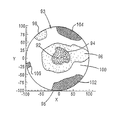
図4と5のコイルが図1のプロセッサの窓19の上部に配置された場合、ウェハ71と同じ位置で静電チャック30に装着された200mmウェハ93のエッチング速度は、図6の領域94、96、98、100、102、104および106で示したようになる。ウェハ93は、図5のウェハ93が図4と5のコイルによる励起から結果的に得られるプラズマと反応することを除いては、図3のエッチ・パターンは、図2に描いたコイルの高周波励起から結果的に得られたものであるが、図3のウェハ71と同じ条件下で同じチェンバでエッチングされた。同じエッチング剤を使用し、図5のウェハの位置決め用切り欠き95が図6で、コイルの中心点50と垂直方向に位置合わせされたウェハの中心点92から垂直に延びる線から時計回りに10°のオフセットを有するようにウェハは同じ位置に位置決めされた。
【0054】
図6に描いたウェハ93の平均エッチング速度は2486オングストローム/分であり、1シグマの標準偏差で0.8%の不均一性であった。中心点92を取り囲む領域94は2467オングストローム/分もしくはそれ未満のエッチング速度を有するが、それに対して領域94を取り囲みかつ中心点92の右に広がる領域96は2467乃至2477オングストローム/分の範囲のエッチング速度を有する。領域96を取り囲みかつ約180°の円弧長にわたってウェハ93の周縁部のかなりの部分に沿って広がる領域100は、2477と2487オングストローム/分の間の範囲のエッチング速度を有する。ウェハの左上の四分円にあって約20°の円弧長にわたってウェハ周縁部に広がる領域98は、領域96と同じエッチング速度範囲を有する。2487オングストローム/分を超えるエッチング速度を有する領域102、104および106は、領域102がウェハ・エッジの右下四分円に概して沿って約70°で広がり、領域104がウェハ右上の四分円の約60°に沿って概して広がり、領域106がウェハ・エッジに沿って中心点92の左側へ約10°広がるようにウェハ93の或る周縁部分に沿った小さな扇形を占める。
【0055】
図4と5のコイルは、前のウェハ71にプラズマ密度を生じさせる図2のコイルのメカニズムとほぼ同じメカニズムでウェハ93上にプラズマ密度を生じさせる。ウェハ93をエッチングするウェハ71の場合よりもさらに優れたプラズマ密度均一性は、図3の非対称領域72乃至80に基づいた図4と5のコイルの形状調整によって達成される。
【0056】
図3と6を比較すると、図3のウェハ71において領域76、78および80に存在したエッチング速度の非対称性が、図6のウェハ93のエッチング速度に存在しないことが明らかである。図6のウェハのエッチング速度は、図3のウェハのエッチング速度よりもかなり均一であり、傾斜した、すなわち非対称の領域76、78および80に見られるような特徴を含まない。領域100は図6のエッチング速度を支配的し、ウェハの面積のほぼ50%にわたって広がる。
【0057】
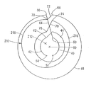
300mmの円形ウェハを処理するのに図1のチェンバが使用されるとき、図5のコイルが図7のコイル100で置き換えられる。図2および5のコイルに似た図7のコイル100は4回の巻線101乃至104を含み、それらのすべてがコイルの中心点106と同心である。内側で、分割巻線101が2つの分離した区画112と114を含み、それぞれが励起端子108と110を含み、それぞれが図1の整合ネットワーク28の出力端子とキャパシタ80に接続される。半径方向かつ円周方向に延びる支柱116、118および120は、支柱116が巻線101の区画112を巻線102の第1の端部に接続し、支柱118が巻線102の第2の端部を巻線103の第1の端部に接続し、支柱120が巻線103の第2の端部を巻線104の第1の端部に接続するように巻線101乃至104の隣り合う対を接続する。支柱122は巻線104の第2の端部を巻線101の整合ネットワーク28の出力端子に接続されていない部分112の端部に接続する。
【0058】
図7のコイル100は、コイル100の巻線101乃至104が、図2、4および5に描かれたコイルの巻線の幾何学形状と異なる幾何学形状を有するので、図2、4および5のコイルとは異なる。特に、巻線103と104は両方共に円形であってそれぞれ8インチ(20.32cm)と6.5インチ(16.41cm)の外側エッジ半径を有する。コイル100の巻線101と102は図2、4および5のコイルの2つの内側巻線と異なるが、その理由は巻線101と102が中心点106に関して非対称だからである。巻線101と巻線102のコイル部分112と114は部分126、128と130を含み、それらはそれぞれ中心点106に関して2インチ(5.08cm)、2インチ(5.08cm)、3.75インチ(9.4cm)の外側エッジ半径を有する円の区画である。部分126、128と130の各々は、支柱116、118、120と122が位置するコイルの側と反対側のコイル100の側で180°の円弧長を有する。
【0059】
図7に描いたように、コイル100は互いに直角をなす水平方向直径131と垂直方向直径133を含む。支柱116乃至120は垂直方向直径133と交差し、それに対して円形部分126、128と130の端部は水平方向直径131と交差する。分割巻線101の部分112と114はそれぞれ相対的に直線の区画132と134を含み、それらは水平方向直径131から上方に、かつ垂直方向直径133に向かっていくぶん内側に延びる。直線区画132と134は垂直方向直径133から約10°のオフセットを有する中心線を有する。区画132は、区画132の端点の先端が水平方向直径131から2.25インチ(6cm)移動するように水平方向直径131から上方に延び、それに対して区画134の直線部分は直径131より3.25インチ(8.80cm)上で終端化する。
【0060】
巻線102は垂直方向直径133の右側と左側で直線区画140と142を含む。区画140と142の各々は垂直方向直径133に向かって約10°の角度で内側に傾斜している。したがって、区画140と142はそれぞれ区画132と134に実質的に平行である。区画142の直線部分は水平方向直径131の約3.4インチ上にある点で終わり、それに対して区画142の直線部分は水平方向直径131の約3.5インチ上にある点で終わる。
【0061】
前記から、コイル100は2つの対称性の外側巻線103と104、および2つの非対称性の内側巻線101と102を含む。非対称性の関係は、コイル100が図2のコイルの示す放射方向非対称束分布の傾向を克服することを可能にし、それに対して巻線103と104のより一層大きい直径は、コイル100が300mm円形ウェハにわたって実質的に均一なプラズマ密度を発生するのを可能にする。
【0062】
図5のコイルから図7のコイルへとコイルを交換することに加えて、200mmウェハプロセッサから300mmウェハプロセッサへと図1のチェンバを置き換えるのに必要となるその他の有意な変更は、200mmと300mmのワークピースのための台座を形成する静電チャックのサイズを変えることである。200mmチャックは300mmウェハにとって適切ではなく、その理由は200mmウェハ用のチャックでウェハの周縁部分に加えられる静電クランプ力は300mmウェハを定位置に保持するのに不十分だからである。300mmウェハ用の静電チャックは200mmウェハに使用することができず、その理由はウェハにとって完全にチャック電極を覆うことが必須だからである。
【0063】
図8は図1に示したタイプのプロセッサで使用することが可能であって、対称性と非対称性の巻線を含むコイルのさらなる実施形態の概略的な上面図である。図8のコイルは、図8のコイルにおける巻線210が図4と5のコイルの巻線182と置き換わっていることを除いて、図4と5のコイルと同様の形状である。図8の巻線210は中心点50から左方向かつ上方向にシフトした中心点212を有する実質的に円形の巻線である。巻線210の半径は巻線44と48の半径の間にあり、約5−1/2インチであることが好ましい。したがって、巻線210の右側の部分216は巻線44の右側に極めて近いが、巻線48の右側から極めて遠く移動している。対照的に、巻線210の左側にある部分218は巻線48の左側に極めて近く、巻線44の左上部分から有意に間隔が開いている。巻線210の左側部分218と巻線48の左側の間の間隔は通気を十分に阻止するものであるべきである。
【0064】
本発明の複数の特定の実施形態を説明および例示してきたが、添付の特許請求項に規定したような本発明の精神および範囲から逸脱することなく、特定して例示および説明した実施形態の詳細部で変形を為し得ることは明らかであろう。例えば、図8の円形の巻線110は、図3のプラズマ密度不均一性を低減するように配列される、巻線110の配置に類似した配置を有する楕円形の巻線または(隣りの巻線への接続のための開環を除いて)閉じた非対称構造を有する他の巻線で置き換えられることもあり得る。
【図面の簡単な説明】
【図1】 本発明の改良型コイルを応用することのできる真空プラズマプロセッサの概略図である。
【図2】 前述したHollandらの特許に述べられたのと実質的に同じ形状を有するコイルの上面図である。
【図3】 図2のコイルを備えた図1のプロセッサで処理されたウェハのエッチング速度を示す上面図である。
【図4】 本発明の好ましい一実施形態による、200mm直径のウェハを処理するのに使用するためのコイルの概略の上面図である。
【図5】 図4に図式的に描いたコイルの上面図である。
【図6】 図4と5のコイルを備えた図1のプロセッサで処理されたウェハのエッチング速度を示す上面図である。
【図7】 直径300mmのウェハを処理するときの図1のプロセッサで使用するためのコイルの上面図である。
【図8】 本発明によるコイルのまた別の実施形態の概略の上面図である。(Field of Invention)
The present invention relates generally to a plasma processor having a radio frequency response coil for exciting a gas in a vacuum chamber into a plasma processing a workpiece in the chamber, and more particularly having substantially symmetric and asymmetric windings. It relates to such a processor comprising a substantially planar coil, and to such a coil. Yet another aspect of the present invention is a method of plasma processing circular workpieces having various diameters, and more particularly, when processing workpieces having various peripheral lengths, the same chamber or the same geometry. The present invention relates to a method in which a plurality of chambers having a shape are coupled to a high-frequency excitation coil having various peripheral dimensions.
[0001]
(Background of the Invention)
One type of processor that processes workpieces with high frequency plasma in a vacuum chamber includes a coil that is responsive to a high frequency power source. This coil generates an electromagnetic field that excites ionizable gas in the chamber into a plasma in response to a high frequency power source. This coil is usually placed on or adjacent to the top of a dielectric window extending in a direction parallel to the flat, horizontally extending surface of the product to be processed. The excited plasma interacts with the workpiece in the chamber to etch the workpiece or deposit material thereon. The workpiece is typically a semiconductor wafer or solid dielectric plate having a flat circular surface, such as a rectangular glass substrate or metal plate used for flat panel displays.
[0002]
Ogle's US Pat. No. 4,948,458 discloses a multi-turn spiral coil to achieve the above results. This spiral, which is generally Archimedean, extends radially and circumferentially between an inner terminal and an outer terminal connected to a high-frequency power source via an impedance matching network. This general type of coil produces an oscillating high frequency field with magnetic and capacitive field components that propagates through a dielectric window to dissipate electrons in some gas in the plasma in the chamber near the window. Heat. An oscillating high frequency field induces a current in the plasma, which heats the electrons in the plasma. The spatial distribution of the magnetic field in the plasma portion near the window is a function of the sum of the individual magnetic field components produced by each winding of the coil. The individual magnetic field components produced by each winding are a function of the magnitude of the high frequency current in each winding, which differs in the various windings due to the coil transmission line effect at the frequency of the high frequency power supply.
[0003]
In the spiral design disclosed in Ogle's 4,948,458 patent, the high-frequency current of the spiral coil is distributed so as to generate a toroidal magnetic field region in the plasma portion near the window, and the power is absorbed by the gas. The gas is excited into the plasma. At low pressures, on the order of 1.0 to 10 mTorr, the diffusion of the plasma from the ring-shaped region generates a plasma density peak just above the center and peripheral workpieces of the chamber, so that the ions that process the workpiece and The electron peak densities are close to the workpiece centerline and the workpiece periphery. In the intermediate pressure range of about 10 to 100 mTorr, gas phase collisions of electrons, ions and neutrons in the plasma prevent substantial diffusion of the plasma charged particles out of the toroidal region. As a result, there is a relatively large plasma bundle in the workpiece ring-shaped region, but a small plasma bundle in the central and peripheral workpiece portions.
[0004]
These different operating conditions result in large variations in the plasma flux (ie plasma density) between the ring and the volume inside and outside the ring, and the standard deviation of the plasma flux incident on the workpiece is increased. A measure of the plasma flux incident on the workpiece is the etch rate expressed in angstroms / minute of the workpiece, and the standard deviation of the etch rate uniformity of an Ogle type coil is typically greater than 3.0%. If the standard deviation of the plasma flux incident on the workpiece is large, the workpiece tends to be processed unevenly, i.e. various parts of the workpiece are etched in different amounts and / or different amounts of molecules are Tends to be deposited.
[0005]
Many coils have been designed to improve plasma uniformity. US Pat. No. 5,759,280 (Holland et al.), Issued on June 2, 1998, by the same applicant, has a diameter of 12 inches in a commercial embodiment and a diameter of the inner wall circle of 14. A coil operating in combination with a vacuum chamber having 0 inches is disclosed. This coil applies an electromagnetic field inside the chamber through a quartz window having a diameter of 14.7 inches and a uniform thickness of 0.8 inches. The center of each workpiece is placed in a workpiece holder, which is a circular semiconductor wafer having a diameter of 200 mm so as to coincide with the center line of the coil, 4.7 inches below the bottom of the window.
[0006]
The coil of the 5,759,280 patent produces significantly less plasma flux variation across the workpiece than the coil of the 4,948,458 patent. In a chamber operating at 5 mm Torr, the standard deviation in etch rate uniformity resulting from the plasma flux generated by the 5,759,280 coil on a 200 mm wafer is about 2.0%. There is a significant improvement over the standard deviation of about 3.0% for the coil of the 4,948,458 patent operating under the same conditions. The coil of the 5,759,280 patent causes a magnetic field in which the plasma density in the center of the workpiece is greater than the plasma density in the middle of the workpiece, and thus exceeds the plasma density in the periphery of the workpiece. . Variations in plasma density in various parts of the chamber with the 5,759,280 coil result in a lower standard deviation and much more than that of the 4,948,458 coil under the same operating conditions small.
[0007]
With the advent of circular semiconductor wafers having a diameter of 300 mm, it has been proposed to use the same vacuum chamber for plasma processing 200 mm and 300 mm diameter circular semiconductor wafers. FIG. 1 is a drawing of a processor that can be used to process wafers of both diameters. In the type of processor depicted in FIG. 1, the same processor is used for both diameters at different times, or a processor with multiple chambers with the same geometry separates 200 mm and 300 mm diameter wafers. Used to process.
[0008]
The vacuum plasma workpiece processor of FIG. 1 has a
[0009]
A suitable ionizable gas that can be excited to a plasma state is supplied into the
[0010]
The gas in the chamber is excited by a suitable power source to provide a plasma having a much more uniform density than the plasma excited by the coil disclosed in Ogle's 4,948,458 patent. The power source includes a substantially
[0011]
An impedance matching
[0012]
A
[0013]
The high
[0014]
Surrounding the
[0015]
The diameter of the
[0016]
The distance between the processing surface of
[0017]
The
[0018]
As depicted in FIG. 2, the
[0019]
[0020]
j = √ (−1), f is the frequency of the high
[0021]
The voltage and current of the
Vpkpk (X)= V0 pkpkcos [β (x + xo)]and
Ipkpk (X)= I0 pkpksin [β (x + xo]]
here,
x is the linear distance measured from the
β is an angular frequency divided by the speed of light c of the high
xoIs an offset from zero determined by the value of
V0 pkpkAnd I0 pkpkAre the maximum high frequency peak peak voltage and current of the coil, respectively.
[0022]
The value of
[0023]
The peripheral region of the
[0024]
Variations in the magnitude of the high-frequency current flowing through the various portions of the coil are averaged in space, helping to inject a more uniform plasma onto the
(Where θ represents the angle about the coil periphery with respect to a reference angle extending through the
[0025]
The constant and spatially averaged magnetic flux along a particular coordinate value θ is more radially symmetric along θ than the resulting plasma from the coil disclosed in Ogle'498 patent. Supply a charged plasma. The amplitudes of the peak peak high frequency currents of the two substantially semi-circular and
[0026]
Electrostatically (ie capacitively) coupling the voltage of various portions of the plate coil 24 (eg, between the
[0027]
It has been found that the smaller the integrated circuit features, the less frequently the uniformity of the plasma incident on the 200 mm wafer generated by the coil described in connection with FIG. When the plasma is excited with the described 13 inch diameter coil, an asymmetric diameter plasma flux distribution is formed on the 200 mm wafer by the processor of FIG. This asymmetry has a significant adverse effect on semiconductor devices having a 0.18 micrometer feature formed on a 200 mm semiconductor wafer. In particular, when a wafer is etched in a vacuum of about 20 mTorr in the processor illustrated in FIG. 1 while exciting the gas in the processor to plasma by the coil of FIG. 2 connected to a high
[0028]
The
[0029]
The generally crescent shaped
[0030]
[0031]
From the analysis of FIG. 3, the plasma density asymmetries associated with
[0032]
Accordingly, it is an object of the present invention to provide a new and improved vacuum plasma processor and radio frequency plasma excitation coil to achieve a highly uniform plasma flux (ie plasma density) on a circular workpiece.
[0033]
An additional object of the present invention is a new type with a high frequency plasma excited by a coil with a new and improved geometry to achieve even greater uniformity of plasma density on a circular workpiece. It is to provide an improved vacuum plasma processor.
[0034]
It is a further object of the present invention to provide a new and improved vacuum plasma processor and coil capable of etching wafers with non-uniformities of less than 1.4% with a standard deviation of 1 sigma.
[0035]
Yet another object of the present invention is an improvement in a new type having a new and improved high frequency excitation coil having a small feature and being particularly suitable for use in the manufacture of integrated circuits smaller than 0.18 microns. It is to provide an improved vacuum plasma processor.
[0036]
An additional object of the present invention is a new and improved method of operating a plasma processor that allows workpieces of the same shape but different sizes to be processed in multiple chambers having the same processing chamber or the same geometry. Is to provide.
[0037]
An additional object of the present invention is to provide a new and improved method of operating a plasma processor such that circular semiconductor wafers having diameters of 200 and 300 mm can be processed in the same processing chamber or multiple chambers having the same geometry. There is to do.
[0038]
(Summary of Invention)
According to one aspect of the invention, for supplying a high frequency plasma excitation field to an ionizable gas of a vacuum plasma processor for a circular workpiece configured to be installed at a specific location on a workpiece holder. The substantially planar coil comprises: (a) a plurality of coaxial windings arranged substantially symmetrically with respect to the center point of the coil; and (b) at least one time arranged asymmetrically with respect to the center point of the coil. Including additional windings.
[0039]
The invention also relates to a vacuum plasma processor having such a coil.
[0040]
Yet another aspect of the invention relates to a vacuum plasma processor for processing circular workpieces that achieve even better plasma density uniformity on the workpiece than other vacuum plasma processors. Other processors include four concentric series-connected circular windings and an excitation terminal centrally connected to a high frequency excitation source. When the other processor is energized, the plasma density along the substantial workpiece arc length on the first side of the workpiece is along the substantial workpiece arc length on the second side of the workpiece. This causes a plasma density distribution on the workpiece that is asymmetric in the diametrical direction that is significantly different from the plasma density. The arc lengths on the first and second sides are substantially opposite to each other in the diametrical direction. The processor includes (a) a vacuum chamber for processing the workpiece with plasma, (b) a holder for the workpiece in the chamber, and (c) a substantially flat plate for exciting the gas in the chamber into the plasma. And (d) a high frequency power source for exciting the coil. The coil is (a) a plurality of circular coaxial concentric windings with a common center point, (b) a central excitation terminal with connections to be driven by a high frequency power source, and (c) a diametrical plasma density. At least one having a different geometry than the other windings to substantially reduce asymmetry and provide a better plasma density uniformity on the workpiece than other plasma processors operating under the same conditions Including additional windings.
[0041]
At least one additional winding is (a) an arcuate portion near the center point aligned with a workpiece portion having a higher plasma density in another processor, and (b) an arcuate portion far from the center point Preferably, it includes a plurality of arcuate portions having different spacings from the center point so that is aligned with a workpiece portion having a lower plasma density with other processors.
[0042]
In one embodiment, the at least one additional winding includes first and second arcuate portions. The first and second portions are circular sectors, with different radii and a common center point that is substantially the same as the center point of the multiple windings. In all of the embodiments of the present invention, it is preferred that at least one additional winding has a closed shape except for a connection to an adjacent winding.
[0043]
In yet another embodiment, the at least one additional winding is a circle having a center that has moved from a common center point to a side of the workpiece having a substantially lower plasma density during processing by other processors. It has the shape of
[0044]
In a preferred embodiment, the coil has only four turns, three of which are multiple turns and only one is at least one further turn. Additional windings are between the multiple windings having the largest radius and the second smallest radius. The excitation terminal is in the winding with the smallest radius. The windings gradually moving away from the center point are directly connected to each other, and the windings having the maximum radius and the minimum radius are also directly connected to each other.
[0045]
In another embodiment, the at least one additional winding is (a) a first portion that is a circular sector having a center point concentric with the center point of the coil, and (b) a first portion of the first portion. A second portion extending substantially linearly from the end of the first portion; and (c) a third portion extending substantially linearly from the second end of the first portion. The first portion is preferably divided into first and second sections having third and fourth ends connected to a high frequency power source, respectively.
[0046]
Such a coil preferably includes first and second further windings. The first further winding is closer to the center point of the coil than the second further winding. Both at least one further winding has the aforementioned shape. The circular sectors of both additional windings are aligned in an arcuate shape. The straight portions of both further windings extend substantially parallel to each other. The first and second further windings are the coil windings closest to the center point of the coil.
[0047]
Further aspects of the present invention have different first and second peripheral lengths and geometrically similar shapes within the same vacuum plasma processing chamber or a plurality of vacuum plasma processing chambers having the same geometry. It relates to a method of processing a workpiece. The method includes coupling a radio frequency plasma excitation coil having first and second different peripheral dimensions to an ionizable gas in a chamber or multiple chambers, between which first and second peripheral length workpieces are formed. Each is processed in a chamber or a plurality of chambers in which high frequency energy is supplied to the coils in order to excite the gas into the processing plasma under vacuum. The first peripheral length exceeds the second peripheral length, and the first peripheral dimension is larger than the second peripheral dimension.
[0048]
The workpiece is circular and each of the coils includes a plurality of substantially circular and coaxial windings having a center point aligned with the center point of the circular workpiece, and each of the coils is a center point of the coil Preferably, it includes at least one winding that is asymmetric with respect to.
[0049]
The above and further objects, features and advantages of the present invention will become apparent upon consideration of the following detailed description of certain specific embodiments, particularly when taken in conjunction with the accompanying drawings.
[0050]
(Detailed description of FIGS. 4 to 8)
The coils of FIGS. 4 and 5 used in the processor of FIG. 1 in place of the coils of FIG. 2 are very similar in construction to the coils of FIG. 2, and the coils of FIGS. 4 and 5 have an outer diameter of 13 inches. , A
[0051]
The main difference between the coils of FIGS. 2 and 4 is that the coil of FIG. 4 includes an asymmetrical winding 182 having
[0052]
Opposing ends 190 of
[0053]
When the coils of FIGS. 4 and 5 are placed on top of the
[0054]
The average etch rate of
[0055]
The coils of FIGS. 4 and 5 generate plasma density on the
[0056]
Comparing FIGS. 3 and 6, it is clear that the etch rate asymmetry that was present in
[0057]
When the chamber of FIG. 1 is used to process a 300 mm circular wafer, the coil of FIG. 5 is replaced with the
[0058]
The
[0059]
As depicted in FIG. 7, the
[0060]
Winding 102 includes
[0061]
From the foregoing, the
[0062]
In addition to replacing the coil from the coil of FIG. 5 to the coil of FIG. 7, other significant changes required to replace the chamber of FIG. 1 from the 200 mm wafer processor to the 300 mm wafer processor are 200 mm and 300 mm. Changing the size of the electrostatic chuck that forms the pedestal for the workpiece. A 200 mm chuck is not suitable for a 300 mm wafer because the electrostatic clamping force applied to the peripheral edge of the wafer with a chuck for a 200 mm wafer is insufficient to hold the 300 mm wafer in place. An electrostatic chuck for a 300 mm wafer cannot be used for a 200 mm wafer because it is essential for the wafer to completely cover the chuck electrode.
[0063]
FIG. 8 is a schematic top view of a further embodiment of a coil that can be used with a processor of the type shown in FIG. 1 and includes symmetric and asymmetric windings. The coil of FIG. 8 is similar in shape to the coil of FIGS. 4 and 5 except that the winding 210 in the coil of FIG. 8 is replaced with the winding 182 of the coil of FIGS. The winding 210 of FIG. 8 is a substantially circular winding having a
[0064]
Although several specific embodiments of the present invention have been described and illustrated, details of the embodiments specifically illustrated and described without departing from the spirit and scope of the present invention as defined in the appended claims. It will be apparent that the part can be deformed. For example, the circular winding 110 of FIG. 8 may be arranged to reduce the plasma density non-uniformity of FIG. It can also be replaced by another winding having a closed asymmetric structure (except for the opening for connection to the line).
[Brief description of the drawings]
FIG. 1 is a schematic diagram of a vacuum plasma processor to which the improved coil of the present invention can be applied.
FIG. 2 is a top view of a coil having substantially the same shape as described in the aforementioned Holland et al. Patent.
3 is a top view showing the etching rate of a wafer processed by the processor of FIG. 1 with the coil of FIG. 2. FIG.
FIG. 4 is a schematic top view of a coil for use in processing a 200 mm diameter wafer according to a preferred embodiment of the present invention.
FIG. 5 is a top view of the coil schematically depicted in FIG. 4;
6 is a top view showing the etch rate of a wafer processed by the processor of FIG. 1 with the coils of FIGS. 4 and 5. FIG.
7 is a top view of a coil for use with the processor of FIG. 1 when processing a 300 mm diameter wafer. FIG.
FIG. 8 is a schematic top view of yet another embodiment of a coil according to the present invention.
Claims (11)
前記ワークピースをプラズマで処理するための真空チェンバと、
前記真空チェンバ内のワークピースホルダと、
前記真空チェンバ内のイオン化可能なガスをプラズマへと励起するための平板状のコイルと、
前記コイルにプラズマ高周波励起電圧を供給するための高周波電源とを含み、
前記真空チェンバは、前記ワークピースが処理中に前記ワークピースホルダの特定の場所に位置するように配置され、
前記コイルは、(a)巻線幅が略等しく、且つ、共通中心からの半径が異なる略円形の複数の巻線と、(b)巻線幅が前記複数の巻線と略等しい少なくとも1つのさらなる巻線が、支柱を介して直列接続された構成を備え、
前記複数の巻線は該巻線の全部の内縁と前記共通中心との間隔が略一定になっている態様を有するのに対し、前記少なくとも1つのさらなる巻線は該巻線の少なくとも一部の内縁と前記共通中心との間隔が略一定になっていない態様を有する、
ことを特徴とする真空プラズマプロセッサ。A vacuum plasma processor for processing circular workpieces,
A vacuum chamber for processing the workpiece with the plasma,
A workpiece holder in the vacuum chamber;
A flat coil for exciting the ionizable gas in the vacuum chamber into a plasma;
A high frequency power source for supplying a plasma high frequency excitation voltage to the coil,
Said vacuum chamber, the workpiece is arranged to be positioned in a specific location of the workpiece holder during processing,
The coil is, (a) winding width approximately equal, and a plurality of windings substantially circular with a radius different from the common center, at least one substantially equal to the plurality of windings (b) winding width A further winding of the configuration is connected in series via a post ,
The plurality of windings have an aspect in which the distance between all inner edges of the windings and the common center is substantially constant, whereas the at least one additional winding is at least part of the windings. A mode in which an interval between an inner edge and the common center is not substantially constant,
A vacuum plasma processor characterized by that.
ことを特徴とする請求項1に記載の真空プラズマプロセッサ。The at least one further winding consists of three sections of continuous arcuate shape, the distance between the inner edge of two of the three sections and the common center being substantially the same, whereas The distance between the inner edge of one of the two sections and the common center is different from the distance between the inner edge of the two sections and the common center.
The vacuum plasma processor according to claim 1 .
ことを特徴とする請求項2に記載の真空プラズマプロセッサ。 The three sections are composed of arc portions having the same center as the common center, and the radius of the arc section configuring the one section is different from the radius of the arc sections configuring the two sections.
The vacuum plasma processor according to claim 2 .
ことを特徴とする請求項1に記載の真空プラズマプロセッサ。The at least one further winding has a substantially circular shape, and the center of the at least one further winding having the substantially circular shape is shifted from the common center in a plane direction of the coil;
The vacuum plasma processor according to claim 1 .
ことを特徴とする請求項1〜4の何れか1項に記載の真空プラズマプロセッサ。Said plurality of windings is two, the is not less one at least one additional winding, said one additional winding Ru mania of the two windings,
The vacuum plasma processor of any one of Claims 1-4 characterized by the above-mentioned.
ことを特徴とする請求項1〜5の何れか1項に記載の真空プラズマプロセッサ。 Before Symbol coil includes a pair of excitation terminals that is disposed on the center of the coil for connection to a terminal that faces the high frequency power source,
The vacuum plasma processor according to any one of claims 1 to 5, wherein:
前記コイルは、(a)巻線幅が略等しく、且つ、共通中心からの半径が異なる略円形の複数の巻線と、(b)巻線幅が前記複数の巻線と略等しい少なくとも1つのさらなる巻線が、支柱を介して直列接続された構成を備え、
前記複数の巻線は該巻線の全部の内縁と前記共通中心との間隔が略一定になっている態様を有するのに対し、前記少なくとも1つのさらなる巻線は該巻線の少なくとも一部の内縁と前記共通中心との間隔が略一定になっていない態様を有する、
ことを特徴とするコイル。A flat coil for supplying a high frequency plasma excitation field to an ionizable gas in a vacuum plasma processor that processes a circular workpiece configured to be placed at a specific location on the workpiece holder. And
The coil is, (a) winding width approximately equal, and a plurality of windings substantially circular with a radius different from the common center, at least one substantially equal to the plurality of windings (b) winding width A further winding of the configuration is connected in series via a post ,
The plurality of windings have an aspect in which the distance between all inner edges of the windings and the common center is substantially constant, whereas the at least one additional winding is at least part of the windings. A mode in which an interval between an inner edge and the common center is not substantially constant,
A coil characterized by that.
ことを特徴とする請求項7に記載のコイル。The at least one further winding consists of three sections of continuous arcuate shape, the distance between the inner edge of two of the three sections and the common center being substantially the same, whereas The distance between the inner edge of one of the two sections and the common center is different from the distance between the inner edge of the two sections and the common center.
The coil according to claim 7 .
ことを特徴とする請求項8に記載のコイル。 The three sections are composed of arc portions having the same center as the common center, and the radius of the arc section configuring the one section is different from the radius of the arc sections configuring the two sections.
The coil according to claim 8 .
ことを特徴とする請求項7に記載のコイル。The at least one further winding has a substantially circular shape, and the center of the at least one further winding having the substantially circular shape is shifted from the common center in a plane direction of the coil;
The coil according to claim 7 .
ことを特徴とする請求項7〜10の何れか1項に記載のコイル。Said plurality of windings is two, the is not less one at least one additional winding, said one additional winding Ru mania of the two windings,
The coil according to any one of claims 7 to 10 , characterized by:
Applications Claiming Priority (3)
| Application Number | Priority Date | Filing Date | Title |
|---|---|---|---|
| US09/607,326 | 2000-06-30 | ||
| US09/607,326 US6531029B1 (en) | 2000-06-30 | 2000-06-30 | Vacuum plasma processor apparatus and method |
| PCT/US2001/020263 WO2002003763A2 (en) | 2000-06-30 | 2001-06-26 | Vacuum plasma processor apparatus and method |
Related Child Applications (1)
| Application Number | Title | Priority Date | Filing Date |
|---|---|---|---|
| JP2011227690A Division JP5538340B2 (en) | 2000-06-30 | 2011-10-17 | Workpiece processing method and vacuum plasma processor |
Publications (3)
| Publication Number | Publication Date |
|---|---|
| JP2004520704A JP2004520704A (en) | 2004-07-08 |
| JP2004520704A5 JP2004520704A5 (en) | 2005-04-07 |
| JP5116203B2 true JP5116203B2 (en) | 2013-01-09 |
Family
ID=24431792
Family Applications (2)
| Application Number | Title | Priority Date | Filing Date |
|---|---|---|---|
| JP2002507035A Expired - Fee Related JP5116203B2 (en) | 2000-06-30 | 2001-06-26 | Vacuum plasma processor and coil |
| JP2011227690A Expired - Fee Related JP5538340B2 (en) | 2000-06-30 | 2011-10-17 | Workpiece processing method and vacuum plasma processor |
Family Applications After (1)
| Application Number | Title | Priority Date | Filing Date |
|---|---|---|---|
| JP2011227690A Expired - Fee Related JP5538340B2 (en) | 2000-06-30 | 2011-10-17 | Workpiece processing method and vacuum plasma processor |
Country Status (8)
| Country | Link |
|---|---|
| US (2) | US6531029B1 (en) |
| EP (1) | EP1300057B1 (en) |
| JP (2) | JP5116203B2 (en) |
| KR (2) | KR100881882B1 (en) |
| AU (1) | AU2001270163A1 (en) |
| DE (1) | DE60128229T2 (en) |
| TW (1) | TW515005B (en) |
| WO (1) | WO2002003763A2 (en) |
Families Citing this family (13)
| Publication number | Priority date | Publication date | Assignee | Title |
|---|---|---|---|---|
| US7571697B2 (en) * | 2001-09-14 | 2009-08-11 | Lam Research Corporation | Plasma processor coil |
| US6876155B2 (en) * | 2002-12-31 | 2005-04-05 | Lam Research Corporation | Plasma processor apparatus and method, and antenna |
| KR100964398B1 (en) * | 2003-01-03 | 2010-06-17 | 삼성전자주식회사 | Inductively coupled antenna and plasma processing apparatus using the same |
| US20040261718A1 (en) * | 2003-06-26 | 2004-12-30 | Kim Nam Hun | Plasma source coil for generating plasma and plasma chamber using the same |
| US7713432B2 (en) * | 2004-10-04 | 2010-05-11 | David Johnson | Method and apparatus to improve plasma etch uniformity |
| US20080003377A1 (en) * | 2006-06-30 | 2008-01-03 | The Board Of Regents Of The Nevada System Of Higher Ed. On Behalf Of The Unlv | Transparent vacuum system |
| DE102008024014A1 (en) * | 2008-05-16 | 2010-04-15 | Ofa Bamberg Gmbh | Device for detecting washing process of clothing item or bandage, comprises data processing unit, which detects whether clothing item or bandage is washed based on signal of optical sensor or transponder, display, and water-tight housing |
| US20120103524A1 (en) * | 2010-10-28 | 2012-05-03 | Applied Materials, Inc. | Plasma processing apparatus with reduced effects of process chamber asymmetry |
| US20120152900A1 (en) * | 2010-12-20 | 2012-06-21 | Applied Materials, Inc. | Methods and apparatus for gas delivery into plasma processing chambers |
| US10777387B2 (en) * | 2012-09-28 | 2020-09-15 | Semes Co., Ltd. | Apparatus for treating substrate |
| CN109036817B (en) * | 2017-06-08 | 2021-09-17 | 北京北方华创微电子装备有限公司 | Inductive coupling coil and process chamber |
| JP6909824B2 (en) * | 2019-05-17 | 2021-07-28 | 株式会社Kokusai Electric | Substrate processing equipment, semiconductor equipment manufacturing methods and programs |
| KR20220107521A (en) * | 2021-01-25 | 2022-08-02 | (주) 엔피홀딩스 | Reactor, process processing apparatus including the same and method for manufacturing reactor |
Family Cites Families (18)
| Publication number | Priority date | Publication date | Assignee | Title |
|---|---|---|---|---|
| US4948458A (en) | 1989-08-14 | 1990-08-14 | Lam Research Corporation | Method and apparatus for producing magnetically-coupled planar plasma |
| US6077384A (en) | 1994-08-11 | 2000-06-20 | Applied Materials, Inc. | Plasma reactor having an inductive antenna coupling power through a parallel plate electrode |
| US5401350A (en) | 1993-03-08 | 1995-03-28 | Lsi Logic Corporation | Coil configurations for improved uniformity in inductively coupled plasma systems |
| US5919382A (en) * | 1994-10-31 | 1999-07-06 | Applied Materials, Inc. | Automatic frequency tuning of an RF power source of an inductively coupled plasma reactor |
| US5838111A (en) | 1996-02-27 | 1998-11-17 | Matsushita Electric Industrial Co., Ltd. | Plasma generator with antennas attached to top electrodes |
| US6268700B1 (en) * | 1996-06-10 | 2001-07-31 | Lam Research Corporation | Vacuum plasma processor having coil with intermediate portion coupling lower magnetic flux density to plasma than center and peripheral portions of the coil |
| US5759280A (en) | 1996-06-10 | 1998-06-02 | Lam Research Corporation | Inductively coupled source for deriving substantially uniform plasma flux |
| US5800619A (en) | 1996-06-10 | 1998-09-01 | Lam Research Corporation | Vacuum plasma processor having coil with minimum magnetic field in its center |
| CA2207154A1 (en) | 1996-06-10 | 1997-12-10 | Lam Research Corporation | Inductively coupled source for deriving substantially uniform plasma flux |
| JP3658922B2 (en) | 1997-05-22 | 2005-06-15 | 松下電器産業株式会社 | Plasma processing method and apparatus |
| EP1327498B1 (en) | 1997-04-08 | 2013-06-12 | Ebara Corporation | Polishing apparatus |
| US6028285A (en) | 1997-11-19 | 2000-02-22 | Board Of Regents, The University Of Texas System | High density plasma source for semiconductor processing |
| JP2972707B1 (en) * | 1998-02-26 | 1999-11-08 | 松下電子工業株式会社 | Plasma etching apparatus and plasma etching method |
| US6146508A (en) * | 1998-04-22 | 2000-11-14 | Applied Materials, Inc. | Sputtering method and apparatus with small diameter RF coil |
| US6164241A (en) * | 1998-06-30 | 2000-12-26 | Lam Research Corporation | Multiple coil antenna for inductively-coupled plasma generation systems |
| KR100291898B1 (en) * | 1999-04-09 | 2001-06-01 | 윤종용 | Method of making shield and plasma etching apparatus for enhanced inductive coupling to plasmas with reduced sputter contamination |
| US6319355B1 (en) * | 1999-06-30 | 2001-11-20 | Lam Research Corporation | Plasma processor with coil responsive to variable amplitude rf envelope |
| US6143144A (en) * | 1999-07-30 | 2000-11-07 | Tokyo Electronlimited | Method for etch rate enhancement by background oxygen control in a soft etch system |
-
2000
- 2000-06-30 US US09/607,326 patent/US6531029B1/en not_active Expired - Lifetime
-
2001
- 2001-06-26 EP EP01948718A patent/EP1300057B1/en not_active Expired - Lifetime
- 2001-06-26 WO PCT/US2001/020263 patent/WO2002003763A2/en active IP Right Grant
- 2001-06-26 KR KR1020027017794A patent/KR100881882B1/en not_active IP Right Cessation
- 2001-06-26 AU AU2001270163A patent/AU2001270163A1/en not_active Abandoned
- 2001-06-26 KR KR1020077014974A patent/KR100807143B1/en not_active IP Right Cessation
- 2001-06-26 DE DE60128229T patent/DE60128229T2/en not_active Expired - Lifetime
- 2001-06-26 JP JP2002507035A patent/JP5116203B2/en not_active Expired - Fee Related
- 2001-07-11 TW TW090116008A patent/TW515005B/en not_active IP Right Cessation
-
2003
- 2003-01-21 US US10/347,363 patent/US6897156B2/en not_active Expired - Fee Related
-
2011
- 2011-10-17 JP JP2011227690A patent/JP5538340B2/en not_active Expired - Fee Related
Also Published As
| Publication number | Publication date |
|---|---|
| JP5538340B2 (en) | 2014-07-02 |
| JP2004520704A (en) | 2004-07-08 |
| DE60128229D1 (en) | 2007-06-14 |
| US20030106645A1 (en) | 2003-06-12 |
| WO2002003763B1 (en) | 2003-03-13 |
| US6897156B2 (en) | 2005-05-24 |
| DE60128229T2 (en) | 2007-08-30 |
| KR100881882B1 (en) | 2009-02-06 |
| KR20030034108A (en) | 2003-05-01 |
| KR20070074672A (en) | 2007-07-12 |
| AU2001270163A1 (en) | 2002-01-14 |
| WO2002003763A2 (en) | 2002-01-10 |
| EP1300057A2 (en) | 2003-04-09 |
| JP2012033958A (en) | 2012-02-16 |
| WO2002003763A8 (en) | 2002-04-04 |
| WO2002003763A3 (en) | 2002-12-27 |
| EP1300057B1 (en) | 2007-05-02 |
| KR100807143B1 (en) | 2008-02-27 |
| TW515005B (en) | 2002-12-21 |
| US6531029B1 (en) | 2003-03-11 |
Similar Documents
| Publication | Publication Date | Title |
|---|---|---|
| JP5538340B2 (en) | Workpiece processing method and vacuum plasma processor | |
| US5759280A (en) | Inductively coupled source for deriving substantially uniform plasma flux | |
| US5800619A (en) | Vacuum plasma processor having coil with minimum magnetic field in its center | |
| EP1204134B1 (en) | RF plasma processor | |
| JP4387471B2 (en) | Magnetically excited plasma chamber with non-uniform magnetic field | |
| US6441555B1 (en) | Plasma excitation coil | |
| JP5031159B2 (en) | Plasma processor having a coil responsive to a variable amplitude high frequency envelope | |
| US7571697B2 (en) | Plasma processor coil | |
| US6893533B2 (en) | Plasma reactor having a symmetric parallel conductor coil antenna | |
| JPH0888190A (en) | Plasma treatment equipment and plasma treatment method | |
| JP2006518915A (en) | Antenna for uniform processing rate | |
| US6667577B2 (en) | Plasma reactor with spoke antenna having a VHF mode with the spokes in phase | |
| US8956500B2 (en) | Methods to eliminate “M-shape” etch rate profile in inductively coupled plasma reactor | |
| KR100404723B1 (en) | Device for Generating Inductively Coupled Plasma with Lower Aspect Ratio |
Legal Events
| Date | Code | Title | Description |
|---|---|---|---|
| A621 | Written request for application examination |
Free format text: JAPANESE INTERMEDIATE CODE: A621 Effective date: 20080610 |
|
| A977 | Report on retrieval |
Free format text: JAPANESE INTERMEDIATE CODE: A971007 Effective date: 20110414 |
|
| A131 | Notification of reasons for refusal |
Free format text: JAPANESE INTERMEDIATE CODE: A131 Effective date: 20110418 |
|
| A601 | Written request for extension of time |
Free format text: JAPANESE INTERMEDIATE CODE: A601 Effective date: 20110628 |
|
| A602 | Written permission of extension of time |
Free format text: JAPANESE INTERMEDIATE CODE: A602 Effective date: 20110705 |
|
| A601 | Written request for extension of time |
Free format text: JAPANESE INTERMEDIATE CODE: A601 Effective date: 20110817 |
|
| A602 | Written permission of extension of time |
Free format text: JAPANESE INTERMEDIATE CODE: A602 Effective date: 20110824 |
|
| A521 | Request for written amendment filed |
Free format text: JAPANESE INTERMEDIATE CODE: A523 Effective date: 20110915 |
|
| A601 | Written request for extension of time |
Free format text: JAPANESE INTERMEDIATE CODE: A601 Effective date: 20110915 |
|
| A602 | Written permission of extension of time |
Free format text: JAPANESE INTERMEDIATE CODE: A602 Effective date: 20110926 |
|
| A131 | Notification of reasons for refusal |
Free format text: JAPANESE INTERMEDIATE CODE: A131 Effective date: 20120323 |
|
| A601 | Written request for extension of time |
Free format text: JAPANESE INTERMEDIATE CODE: A601 Effective date: 20120622 |
|
| A602 | Written permission of extension of time |
Free format text: JAPANESE INTERMEDIATE CODE: A602 Effective date: 20120629 |
|
| A601 | Written request for extension of time |
Free format text: JAPANESE INTERMEDIATE CODE: A601 Effective date: 20120720 |
|
| A602 | Written permission of extension of time |
Free format text: JAPANESE INTERMEDIATE CODE: A602 Effective date: 20120727 |
|
| A601 | Written request for extension of time |
Free format text: JAPANESE INTERMEDIATE CODE: A601 Effective date: 20120820 |
|
| A602 | Written permission of extension of time |
Free format text: JAPANESE INTERMEDIATE CODE: A602 Effective date: 20120827 |
|
| A521 | Request for written amendment filed |
Free format text: JAPANESE INTERMEDIATE CODE: A523 Effective date: 20120910 |
|
| TRDD | Decision of grant or rejection written | ||
| A01 | Written decision to grant a patent or to grant a registration (utility model) |
Free format text: JAPANESE INTERMEDIATE CODE: A01 Effective date: 20121002 |
|
| A01 | Written decision to grant a patent or to grant a registration (utility model) |
Free format text: JAPANESE INTERMEDIATE CODE: A01 |
|
| A61 | First payment of annual fees (during grant procedure) |
Free format text: JAPANESE INTERMEDIATE CODE: A61 Effective date: 20121016 |
|
| R150 | Certificate of patent or registration of utility model |
Free format text: JAPANESE INTERMEDIATE CODE: R150 |
|
| FPAY | Renewal fee payment (event date is renewal date of database) |
Free format text: PAYMENT UNTIL: 20151026 Year of fee payment: 3 |
|
| R250 | Receipt of annual fees |
Free format text: JAPANESE INTERMEDIATE CODE: R250 |
|
| LAPS | Cancellation because of no payment of annual fees |