JP5113986B2 - MEMS element for adaptive control optical mirror - Google Patents
MEMS element for adaptive control optical mirror Download PDFInfo
- Publication number
- JP5113986B2 JP5113986B2 JP2005064702A JP2005064702A JP5113986B2 JP 5113986 B2 JP5113986 B2 JP 5113986B2 JP 2005064702 A JP2005064702 A JP 2005064702A JP 2005064702 A JP2005064702 A JP 2005064702A JP 5113986 B2 JP5113986 B2 JP 5113986B2
- Authority
- JP
- Japan
- Prior art keywords
- substrate
- coupled
- plate
- rotatable object
- upright spring
- Prior art date
- Legal status (The legal status is an assumption and is not a legal conclusion. Google has not performed a legal analysis and makes no representation as to the accuracy of the status listed.)
- Expired - Fee Related
Links
Images


Classifications
-
- G—PHYSICS
- G02—OPTICS
- G02B—OPTICAL ELEMENTS, SYSTEMS OR APPARATUS
- G02B26/00—Optical devices or arrangements for the control of light using movable or deformable optical elements
- G02B26/08—Optical devices or arrangements for the control of light using movable or deformable optical elements for controlling the direction of light
- G02B26/0816—Optical devices or arrangements for the control of light using movable or deformable optical elements for controlling the direction of light by means of one or more reflecting elements
- G02B26/0833—Optical devices or arrangements for the control of light using movable or deformable optical elements for controlling the direction of light by means of one or more reflecting elements the reflecting element being a micromechanical device, e.g. a MEMS mirror, DMD
- G02B26/0841—Optical devices or arrangements for the control of light using movable or deformable optical elements for controlling the direction of light by means of one or more reflecting elements the reflecting element being a micromechanical device, e.g. a MEMS mirror, DMD the reflecting element being moved or deformed by electrostatic means
Landscapes
- Physics & Mathematics (AREA)
- General Physics & Mathematics (AREA)
- Optics & Photonics (AREA)
- Micromachines (AREA)
- Mechanical Light Control Or Optical Switches (AREA)
Description
本発明は、適応制御光学に関し、より詳細には適応制御光学に用いられる微小電子機械システム(MEMS)に関する。 The present invention relates to adaptive control optics, and more particularly to a microelectromechanical system (MEMS) used for adaptive control optics.
本願の主題は、2004年2月5日出願の米国特許出願第10/772,847号、整理番号Greywall31の主題に関連し、同出願は参照により本明細書に組み込まれる。 The subject matter of this application is related to the subject matter of US patent application Ser. No. 10 / 772,847, filed Feb. 5, 2004, docket number Greywall 31, which is incorporated herein by reference.
適応制御光学は、光信号が伝播する環境が信号に及ぼすひずみについての情報を用いて、光信号を改善する光学の一分野である。この主題についての優れた入門書として「Principles of Adaptive Optics」by R.K.Tyson、Academic Press、San Diego、1991があり、その教示は参照により本明細書に組み込まれる。 Adaptive control optics is a field of optics that uses optical information to improve the optical signal using information about the distortion that the environment in which the optical signal propagates has. An excellent introductory book on this subject is “Principles of Adaptive Optics” by R.D. K. There is Tyson, Academic Press, San Diego, 1991, the teachings of which are incorporated herein by reference.
適応制御光学要素の代表的な例は、波面センサによって駆動され、望遠鏡の像に影響を与える環境ひずみを補償するように構成された可変形ミラーである。自然に発生する大気中の小さな温度変化(約1℃)が、不規則に乱れた空気の動きを引き起こし、また大気密度の変化を引き起こし、その結果屈折率の変化を引き起こす。光線が伝播する経路に沿ったこれら変化の累積効果により、光線がふらついたり、広がったり、強度が変動したりすることが起こり得て、そのどれもが像の品質を低下させる。波面センサは、大気中で受けたひずみを測定し、可変形ミラーへのフィードバック信号を生成する素子である。フィードバック信号に基いて、光線のひずみを大幅に減少させるように可変形ミラーが変形し、それによって像の品質が改善される。 A typical example of an adaptive control optical element is a deformable mirror driven by a wavefront sensor and configured to compensate for environmental distortions affecting the telescope image. Naturally occurring small temperature changes in the atmosphere (about 1 ° C.) cause irregularly turbulent air movements and also changes in atmospheric density, resulting in refractive index changes. Due to the cumulative effect of these changes along the path along which the light propagates, the light can fluctuate, spread, or vary in intensity, all of which degrade the image quality. The wavefront sensor is an element that measures strain received in the atmosphere and generates a feedback signal to the deformable mirror. Based on the feedback signal, the deformable mirror is deformed to significantly reduce the distortion of the light beam, thereby improving the image quality.
可変形ミラーでよく用いられるタイプの1つはセグメントに分割したミラーであり、このミラーでは、各セグメント(ピクセル)が個々に平行移動し、かつ/または回転することができる。多くの用途では、分割型ミラーは、(1)セグメントごとの平行移動/回転の大きさがそれぞれ1μm/10°程度であり、(2)ミラー全体としては、充填率が少なくとも98%である必要がある。しかし、従来技術による多くの設計では、これらの要求が互いに直接対立してしまい、満足することが難しく不可能なことすらある。たとえば、高充填率の要求に対する解決法としては、ミラー支持要素および駆動体をミラーの下に(下に隠して)配置することが考えられる。この配置による結果の一つとして、各セグメントがミラー面の下方に位置する軸の周りを回転することになり、その結果、回転中、ミラー面内の横方向変位を伴うことになる。この変位によって生じる隣接するミラー・セグメントとの物理的干渉を避けるために、セグメント同士の間に比較的大きな間隔が必要になる。しかしこうすると、充填率が大幅に低下する。
本発明の原理によれば、従来技術における問題点は、ミラー平面内に位置する軸まわりで可動ミラー・ピクセルが回転できるように、基板上に支持され、ミラー・ピクセルと基板の間に配置された作動アクチュエータに結合された、可動ミラー・ピクセルを有するMEMS素子によって対処される。 In accordance with the principles of the present invention, a problem with the prior art is that the movable mirror pixel is supported on and placed between the mirror pixel and the substrate so that the movable mirror pixel can rotate about an axis located in the mirror plane. Addressed by a MEMS element having a movable mirror pixel coupled to an actuated actuator.
本発明の一つの実施形態では、作動アクチュエータが可動電極を有し、その可動電極上にミラー・ピクセルが取り付けられている。可動電極は1対の直立ばねによって基板上に支持されており、直立ばねのそれぞれが、ばねの一方の端部で互いに結合し、他方の端部では分離している平行な2つのセグメントを有する。分離しているセグメント端部の一方は基板に結合され、分離しているセグメント端部の他方は可動電極に結合されている。結合しているセグメント端部に対応する直立ばねの端部が基板から遠ざかる方に向けられて、(i)ミラー・ピクセル中の狭いスロットを貫通してばね本体が突き出し、(ii)直立ばねのほぼ中央にミラー面が来るようになっている。有利には、本発明の実施形態に従って実現されたミラー・ピクセルは、回転中の横方向変位が比較的小さく、ミラー支持構造体がミラー面内で占める表面積が比較的小さい。それにより、ミラー・ピクセルの間隔が密で約98%以上の充填率をもたらすセグメント型ミラーが実現できる。 In one embodiment of the invention, the actuating actuator has a movable electrode on which a mirror pixel is mounted. The movable electrode is supported on the substrate by a pair of upright springs, each of the upright springs having two parallel segments that are joined together at one end of the spring and separated at the other end. . One of the separated segment ends is coupled to the substrate, and the other of the separated segment ends is coupled to the movable electrode. The end of the upright spring corresponding to the joining segment end is directed away from the substrate, (i) the spring body projects through a narrow slot in the mirror pixel, and (ii) the upright spring The mirror surface comes to the center. Advantageously, mirror pixels implemented in accordance with embodiments of the invention have a relatively small lateral displacement during rotation and a relatively small surface area occupied by the mirror support structure in the mirror plane. Thereby, a segmented mirror can be realized in which the mirror pixels are closely spaced and a filling factor of about 98% or more is achieved.
本発明の別の実施形態では、MEMS素子は基板上に支持された直立ばねを有する。直立ばねは、ばねの一方の端部で互いに結合し、他方の端部では分離している2つのセグメントを有する。直立ばねは、結合しているセグメント端部の方が、分離しているセグメント端部より基板から遠くなるように基板に対して配置される。分離しているセグメント端部の一方は基板に結合され、分離している端部の他方ははさみ型動作により最初の一方の端部に対して移動できるようになされている。 In another embodiment of the invention, the MEMS element has an upright spring supported on a substrate. An upright spring has two segments that are joined together at one end of the spring and separated at the other end. The upright spring is positioned relative to the substrate such that the joined segment ends are farther from the substrate than the separated segment ends. One of the separated segment ends is coupled to the substrate, and the other of the separated ends is movable relative to the first one end by a scissor-type operation.
図1は、本発明の原理にしたがって構成された、適応制御光学ミラーのピクセルを動かすのに用いることができる例示的なMEMS素子100を示す3次元透視図である。素子100は、作動アクチュエータ110に結合された可動プレート102を有する。プレート102は、プレートと、基板170に取り付けられた支柱104a、bの1つとの間にそれぞれ連結された1対のトーション・ロッド106a、bによって支持される。ロッド106a、bは、図1の破線ABで示されるプレート102の回転軸を規定する。
FIG. 1 is a three-dimensional perspective view illustrating an
アクチュエータ110は、2個の側方電極112a、bおよび中間電極114で形成されるフリンジフィールドアクチュエータである。側方電極112aおよびbは基板170に取り付けられ、したがって静止している。それとは逆に、中間電極114は、リンク・ロッド116によってプレート102に取り付けられ、したがってプレートと共に基板170に対して動くことができる。中間電極114が側方電極112の1つに向かって動くと、リンク・ロッド116が中間電極の動きをプレート102に伝え、それによりプレートが軸ABの周りを回転する。
The
側方電極112のそれぞれは、絶縁層180によって基板170から電気的に絶縁されており、基板に対して電気的にバイアスさせることができる。それとは逆に、中間電極114は、リンク・ロッド116、プレート102、トーション・ロッド106、および支柱104を介して基板170に電気的に接触している。したがって、電極112および114を相互に電気的にバイアスさせて、プレート102を動かすことができる。たとえば、側方電極112aを中間電極114に対してバイアスさせ側方電極112bはバイアスさせずにおくと、中間電極はバイアスさせた電極に向かって引き寄せられ、それにより、それに対応する方向にプレート102が回転する。トーション・ロッド106の歪弾性力が電極間の静電引力と釣り合うと、プレート102が静止する。バイアスが除かれると、弾性力によってプレート102および中間電極114は初期位置に戻る。同様に、側方電極112bを中間電極114に対してバイアスさせ側方電極112aはバイアスさせずにおくと、プレート102は反対方向へ回転する。
Each of the side electrodes 112 is electrically insulated from the
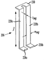
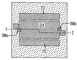
図2A〜Cに本発明の別の実施形態を示す。より具体的には、図2AはMEMS素子200の3次元透視図であり、図2Bは素子200に用いられるばね206の3次元透視図であり、図2Cはプレートの回転可能範囲を示す素子200の側面図である。
2A-C illustrate another embodiment of the present invention. More specifically, FIG. 2A is a three-dimensional perspective view of the
図2Aを参照すると、素子200は図1の素子100に類似しており、同様に適応制御光学ミラーのピクセルを実現するのに用いることができる。素子200は、基板270上に支持され、素子100のアクチュエータ110と同様な作動アクチュエータ210に結合された可動プレート202を有する。ただし、素子100のトーション・ロッド106a、bの代わりに、素子200では直立ばね206a、bが使用され、図2Bにその1つを詳細に示す。次に図2Aおよび図2Bを参照すると、各直立ばね206は2つの基部226a、bを有し、その一方は支持柱204a、bのうちの対応する1本に結合され、他方はアクチュエータ210の中間電極214に結合されている。各直立ばね206は、2つのばねセグメント228a、bを有し、そのばねセグメント228a、bは、図2Cに示すように、プレート202には接触せずに、プレートのスロット(開口)208を通って突き出ている。ばねセグメント228aとbは直立ばね206の上端でブリッジ230によって結合されている。好ましい実装形態では、セグメント228の幅および厚さ(Wsegおよびtseg)は、直立ばね206が、図2Cに示す「はさみ」型のばね変形を比較的容易に許しながら、基板270の面に直交する方向に沿う圧縮に耐える(すなわち長手方向に高い剛性を有する)ような幅および厚さである。
Referring to FIG. 2A,
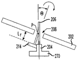
次に図2Cを参照すると、中間電極214が図2Aに示すバイアスされていない位置から動かされると、直立ばね206の一方の基部は中間電極と一緒に動くが、支柱204にしっかり取り付けられた他方の基部は静止したままである。直立ばね206が長手方向の剛性をもつので、このばねの可動基部に取り付けられた構造物の動きは、図2Cに符号Pで示すばねの中間点(すなわち、半分の長さ)を通る軸周りの単なる回転によって極めて良く近似されることが分かる。したがって、リンク・ロッド216が直立ばね206の約半分の長さLrをもつ場合には、プレート202は、素子100(図1)のプレート102と同様にプレート202の面内に位置する軸の周りを回転する。素子200のいくつかの実装形態では、プレート202の面内でスロット208が占める表面積を、素子100で、プレート102の面内で支柱104およびトーション・ロッド106が占有する対応する面積より大幅に小さくすることができる。これにより、素子200の充填率が素子100の充填率に比べて増加する。
Referring now to FIG. 2C, when the
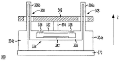
図3に、本発明のさらに別の実施形態によるMEMS素子300を示す。素子300と素子200(図2)は類似しており、両素子の類似の構成要素には、最後の2桁が同じ符号が付されている。ただし、素子300と200の違いの1つは、素子300が、中間電極214の代わりにクレードル構造物334をもつことである。電極214(図2)と同様に、直立ばね306a、bが変形すると、クレードル構造物334が全体として動くことができ、それによりプレート302が基板370に対して回転することができる。しかも、基板370に対する回転に加えて、クレードル構造物334によって、プレート302がZ軸に沿ってクレードル構造物に対するピストン運動ができるようになる。
FIG. 3 illustrates a
クレードル構造物334は、可動プレート332を有し、その上にプレート302が、リンク・ロッド316を用いて取り付けられている。プレート332は、プレート332の面外への変位を許容する1対の蛇行ばね336でクレードル基底338の上に懸架されている。プレート332下方でクレードル基底338に取り付けられた駆動電極342が、プレート332と一緒になって、プレート302を変位させるのに使用できる平行板アクチュエータを形成する。たとえば、電極342がプレート332に対してバイアスされると、静電引力を発生してプレート332を電極に向かって引き付け、それによりプレート302がクレードル構造物334に対して変位する。バイアスが除かれると、ばね336がプレート332および302を初期位置に戻す。
The
図4に、本発明のさらに別の実施形態によるMEMS素子400の3次元透視図を示す。図2の素子200と同様に、素子400は可動プレートをそのプレートの面内に位置する軸周りに回転させる。ただし、可動プレートが単一の軸周りに回転する素子200とは違って、素子400の可動プレートは異なる2軸の周りを回転することができ、それにより、プレートを所望のいかなる方向にでも傾けられる能力が得られる。
FIG. 4 shows a three-dimensional perspective view of a
素子400は、基板470上に支持され、作動アクチュエータ410に結合された可動プレート402を有する。プレート402は、外側リング452および内側ディスク454を有するジンバル構造450上にリンク・ロッド416を用いて取り付けられている。外側リング452は1対の直立ばね406a、bによって支持され、直立ばねはそれぞれ、外側リングと、基板470に取り付けられた支柱404a、bの1つとの間に取り付けられている。内側ディスク454は、内側ディスクと外側リング452との間にそれぞれ取り付けられたもう1対の直立ばね406c、dによって支持される。直立ばね406a〜dはそれぞれ、図2Bに示された直立ばね206に類似し、プレート402の対応するスロット408を通って突き出ている。好ましい実装形態では、リンク・ロッド416の長さはばね406の長さの約半分であり、その結果、ばね406a、bで規定される回転軸(図4の軸AB)および軸406c、dで規定される回転軸(図4の軸CD)がプレート402の面内に来る。図4の実施形態では軸ABと軸CDは互いに直交しているが、別の軸方向を用いることもできる。
アクチュエータ410は、3個の側方電極412a〜cおよび中間電極414を備えるフリンジフィールドアクチュエータである。各側方アクチュエータ412は、たとえば図2Aの側方電極212に類似し、中間電極414は図2Aの中間電極214に類似している。中間電極414が初期位置から側方電極412に向かって偏位すると、リンク・ロッド456が中間電極の動きをジンバル構造450の内側ディスク454に伝え、それにより、さらに以下に説明するように内側ディスクを回転させる。
The
中間電極414が偏位する方向は、側方電極412a〜cに加えられる電圧によって決まる。一般に、中間電極414は、バイアス電圧を適切に組み合わせて加えることによって、選択されたいかなる方向にでも偏位させることができる。たとえば、基板470に直交し軸ABを通る平面が側方電極412bの対称面であると仮定する。すると、側方電極412bが中間電極414に対してバイアスされ、他の側方電極412aおよび412cはバイアスされていないときは、中間電極は電極412bに向かって、軸ABの基板470上への投影に沿って引き寄せられる。その結果、ディスク454が、したがってプレート402が軸CD周りに回転する。同様に、中間電極414を軸CDの投影に沿って引き寄せるように電極412a〜cをバイアスさせると、ディスク454とプレート402は軸AB周りに回転する。中間電極414を任意の方向に偏位させることにより、一般に、ディスク454とプレート402が軸ABおよび軸CD両方の周りを回転することが、当業者には理解されよう。
The direction in which the
本発明の素子を製造するのに種々の製造技術を使用することができる。ある実施形態では、上記で参照した米国特許出願第10/772,847号に開示されているのと同様な製造方法が使用できる。簡潔にいうと、製造方法はシリコン・オン・インシュレータ(SOI)ウェーハで始まり、当業者には周知の一連のパターニング、エッチング、およびデポジション工程に続く。パターニング工程はリソグラフィを用いて実施する。エッチング工程は材質に特定のエッチング、たとえば種々のシリコン層に対してはリアクティブ・イオン・エッチング(RIE)、また種々の酸化シリコン層に対してはフッ素をベースにしたエッチングを用いて実施する。デポジション工程は、たとえば化学的気相成長を用いて実施する。さらに別の様々な製造工程の記述を、米国特許第6,201,631号、第5,629,790号、および第5,501,893号に見ることができ、それらの教示は参照により本明細書に組み込まれる。 Various manufacturing techniques can be used to manufacture the device of the present invention. In certain embodiments, manufacturing methods similar to those disclosed in US patent application Ser. No. 10 / 772,847 referenced above may be used. Briefly, the manufacturing method begins with a silicon-on-insulator (SOI) wafer, followed by a series of patterning, etching, and deposition steps well known to those skilled in the art. The patterning process is performed using lithography. The etching process is performed using material specific etching, such as reactive ion etching (RIE) for various silicon layers and fluorine-based etching for various silicon oxide layers. The deposition process is performed using, for example, chemical vapor deposition. Further various manufacturing process descriptions can be found in US Pat. Nos. 6,201,631, 5,629,790, and 5,501,893, the teachings of which are hereby incorporated by reference. Incorporated in the description.
米国特許出願第10/772,847号でも可撓性の垂直ビームの製造法を開示しており、その垂直ビームは、どちらのタイプの構造も基板の面に実質的に垂直に延びているという点で、本発明のいくつかの実施形態(たとえば図2のばね206)の垂直ばねと類似している。ただし、可撓性垂直ビームは可動プレートと基板の間の空間内に限られているが、垂直ばねは対応する可動プレートを貫通して突き出している。この違いがあるので、垂直ばねの突き出し構造を作り出すことに関連する製造工程を以下により詳しく説明する。
US patent application Ser. No. 10 / 772,847 also discloses a method for producing a flexible vertical beam, which both types of structures extend substantially perpendicular to the plane of the substrate. In that respect, it is similar to the vertical spring of some embodiments of the present invention (eg,
図5A〜Fに、本発明の一実施形態による素子200の代表的な製造工程を概略的に示す。より具体的には、図5A、5C、および5Eは、それぞれの製造工程中の素子200の上面図であり、図5B、5D、および5Fはそれらに対応する側面断面図である。
5A to F schematically illustrate a typical manufacturing process of the
図5A、Bを参照すると、ある実施形態では、(i)2つのシリコン層、すなわちハンドル・レイヤ562およびオーバ・レイヤ566と、(ii)オーバ・レイヤ566とハンドル・レイヤ562の間に配置された酸化シリコン層564とを有するシリコン・オン・インシュレータ(SOI)ウェーハから、素子500の製造が始まる。プレート502を、リアクティブ・エッチングを用いてオーバ・レイヤ566中に形成する。そのエッチングは酸化シリコン層で止まる。開口208a、b(図2も参照)を、オーバ・レイヤ566および酸化シリコン層564の対応する部分をエッチングで取り除いて作り出す。時限式のエッチングをハンドル・レイヤ562に適用して、将来の直立ばね206がプレート202の上に突き出す(図2参照)長さに対応する深さを有する縦穴を作り出す。
Referring to FIGS. 5A, B, in one embodiment, (i) two silicon layers are disposed between
図5C、Dを参照すると、先ず、相対的に厚い(たとえば5μm)酸化シリコン層568を、図5A、Bの構造上に堆積させる。次いで、プレート202と中間電極214を連結するリンク・ロッド216用の開口580を形成するために、層568をパターニングし、エッチングする。次いで、薄い(たとえば1μm)多結晶シリコン層572を、層568の上に堆積させる。層572の開口580を満たす部分が、リンク・ロッド216を作り出す。最後に、開口208に対応する縦穴から多結晶シリコンを取り除くために、層572をパターニングし、エッチングする。
Referring to FIGS. 5C and D, a relatively thick (eg, 5 μm)
図5E、Fを参照すると、先ず、薄い(たとえば0.5μm)多結晶シリコン層574を、図5C、Dの構造上に堆積する。この層は、開口208に対応する縦穴の縦壁を含めて、その構造の露出面を全て覆う。次いで、層572および574を含む複合シリコン層を、パターニングしエッチングして、中間電極214、側方電極212、および直立ばね206を形成する。詳細には、直立ばね206のブリッジ230(図2B参照)は、レイヤ574の、対応する縦穴の底部に位置する部分から形成され、直立ばね206のばねセグメント228a、b(図2B参照)は、層574の、縦穴の縦壁の1つに位置する部分から形成され、直立ばね206の2つの基部226a、bは、層574の、縦穴の上端周辺近くに堆積した部分から形成される。酸化シリコン568が、直立ばね206がプレート202に接触するのを防いでいることに留意されたい。
Referring to FIGS. 5E and F, a thin (eg, 0.5 μm)
製造工程はさらに直截的に続き、支持柱204a,bおよび基板270を図5E、Fの構造の上に形成(図2も参照)する。酸化層を全て取り除く(たとえばエッチングで取り除く)と、素子200の最終構造が現れる。酸化シリコン層564および568が取り除かれた後は、ハンドル(・シリコン)・レイヤ562が最終構造からすっかり分離することに留意されたい。また、図5B、5D、および5Fに示した図は、図2Aに示した図に対し転倒している(逆さになっている)ことにも留意されたい。
The manufacturing process continues further straightforwardly, and support posts 204a, b and
本発明を例示的な実施形態に関して説明してきたが、この説明を限定的な意味に解釈すべきではない。本発明に関する技術分野の技術者にとって明らかな、ここに記述された実施形態に対する様々な変更形態、ならびに本発明の他の実施形態は、添付の特許請求の範囲に記述された本発明の原理および範囲に含まれるものとみなされる。 While this invention has been described with reference to illustrative embodiments, this description should not be construed in a limiting sense. Various modifications to the embodiments described herein, as well as other embodiments of the invention, which will be apparent to those skilled in the art to which the invention pertains, are described in accordance with the principles of the invention as set forth in the appended claims and It is considered to be included in the scope.
本発明によるMEMS素子の製造法を、シリコン/酸化シリコンSOIを使用する場合について説明してきたが、ゲルマニウム補償シリコンのような他の適切な材料を同様に用いてもよい。材料は、公知のように適当に不純物を添加してもよい。それぞれの表面は、たとえば反射率および/または導電率を向上させるために金属を堆積したり、機械的強度を向上するためにイオンを注入したりして、修正してもよい。異なる形状のプレート、ばね、セグメント、ロッド、支柱、アクチュエータ、電極および/または他の素子要素/構造物を、本発明の原理および範囲から逸脱することなく用いることができる。ばねは、種々の形状および大きさを取ることができ、ここで、用語「ばね」とは、一般に、変形した後に元の形状に戻ることができる適切な弾性構造体の全てを指す。直立ばねのばねセグメントは、互いに平行でも、平行でなくてもよい。ミラー・セグメント中の開口(たとえば図2の開口208)は、前記ミラー・セグメントにすっかり囲まれていても、そうでなくてもよい。あるいは、ミラー・セグメントは、直立ばねが前記ミラー・セグメントの外縁の外側を通るような形状でもよい。リンク・ロッド(たとえば図2のリンク・ロッド216)の長さは、対応するミラー・セグメントの回転軸がそのセグメントの面内に来ないように選択してもよい。本発明の様々なMEMS素子を、必要に応じて、かつ/または当分野の技術者にとって自明なように配列することができる。
Although the fabrication method of the MEMS device according to the present invention has been described for the use of silicon / silicon oxide SOI, other suitable materials such as germanium compensated silicon may be used as well. The material may be appropriately doped with impurities as is well known. Each surface may be modified, for example, by depositing metal to improve reflectivity and / or conductivity, or implanting ions to improve mechanical strength. Different shaped plates, springs, segments, rods, struts, actuators, electrodes and / or other element elements / structures can be used without departing from the principles and scope of the present invention. The spring can take a variety of shapes and sizes, where the term “spring” generally refers to all suitable elastic structures that can return to their original shape after being deformed. The spring segments of the upright spring may or may not be parallel to each other. An opening in the mirror segment (eg, opening 208 in FIG. 2) may or may not be completely surrounded by the mirror segment. Alternatively, the mirror segment may be shaped such that an upright spring passes outside the outer edge of the mirror segment. The length of the link rod (eg,
Claims (13)
前記回転可能な物体に取り付けられ、前記第1の偏位距離よりも遠い前記基板からの第2の偏位距離のところに位置する第1のプレートを備え、前記第1のプレートは、前記第1のプレートの面内に位置する回転軸の周りで前記回転可能な物体とともに前記基板に対して回転するようになされており、さらに、
前記回転可能な物体と前記基板との間に結合された直立ばねを備え、
前記直立ばねが、前記直立ばねの一方の端部で互いに結合し、前記直立ばねの他方の端部では分離している2つのセグメントを含み、
分離しているセグメント端部の一方が前記基板に結合され、分離しているセグメント端部の他方が、前記回転可能な物体に結合され、前記基板に対して移動できるようになされ、
前記直立ばねと前記作動アクチュエータとは、前記回転軸の周りで前記回転可能な物体と前記第1のプレートとを回転させることができ、そして、
前記回転可能な物体は、前記第1のプレートに結合され、前記第1のプレートと前記基板の間に配置された可動電極であり、前記可動電極が前記基板に対して移動するとき、前記第1のプレートが前記回転軸の周りで回転する、MEMS素子。 A rotatable object suspended at a first excursion distance from a substrate, the rotatable object being part of an actuating actuator adapted to move the object relative to the substrate; further,
A first plate attached to the rotatable object and positioned at a second excursion distance from the substrate farther than the first excursion distance, the first plate comprising the first excursion; Rotating with respect to the substrate together with the rotatable object about a rotation axis located in the plane of one plate,
An upright spring coupled between the rotatable object and the substrate;
The upright spring includes two segments coupled to each other at one end of the upright spring and separated at the other end of the upright spring;
One of the separated segment ends is coupled to the substrate and the other of the separated segment ends is coupled to the rotatable object and is movable relative to the substrate;
The upright spring and the actuating actuator can rotate the rotatable object and the first plate about the axis of rotation; and
The rotatable object is a movable electrode coupled to the first plate and disposed between the first plate and the substrate, and when the movable electrode moves relative to the substrate, A MEMS element in which one plate rotates around the rotation axis.
前記可動電極が前記静止電極の1つに向かって移動するとき、前記第1のプレートが前記回転軸周りに回転し、
前記可動電極と前記1つまたは複数の静止電極がフリンジ場アクチュエータを形成し、
前記可動電極および前記1つまたは複数の静止電極が、積層ウェーハのただ1つの層を用いて形成される、請求項1に記載の素子。 Further comprising one or more stationary electrodes coupled to the substrate;
When the movable electrode moves toward one of the stationary electrodes, the first plate rotates about the axis of rotation;
The movable electrode and the one or more stationary electrodes form a fringe field actuator;
The device of claim 1, wherein the movable electrode and the one or more stationary electrodes are formed using a single layer of a laminated wafer.
前記回転可能な物体と前記基板との間に結合された直立ばねを備え、
前記直立ばねが、前記直立ばねの一方の端部で互いに結合し、前記直立ばねの他方の端部では分離している2つのセグメントを含み、
分離しているセグメント端部の一方が前記基板に結合され、分離しているセグメント端部の他方が、前記回転可能な物体に結合され、前記基板に対して移動できるようになされ、
前記直立ばねと前記作動アクチュエータとは、前記第1の偏位距離より遠い距離だけ前記基板から偏位する回転軸の周りで前記物体を回転させることができる、MEMS素子。 A rotatable object suspended at a first excursion distance from a substrate, the rotatable object being part of an actuating actuator adapted to move the object relative to the substrate; further,
An upright spring coupled between the rotatable object and the substrate;
The upright spring includes two segments coupled to each other at one end of the upright spring and separated at the other end of the upright spring;
One of the separated segment ends is coupled to the substrate and the other of the separated segment ends is coupled to the rotatable object and is movable relative to the substrate;
The upright spring and the actuating actuator may rotate the object about a rotation axis that is displaced from the substrate by a distance that is greater than the first displacement distance.
前記直立ばねが、前記基板から前記構造物の先まで延び、前記構造物中の開口を貫通して突き出る、請求項4に記載の素子。 A structure mounted on the rotatable object and further disposed at a second excursion distance from the substrate that is farther than the first excursion distance;
The element of claim 4, wherein the upright spring extends from the substrate to the end of the structure and protrudes through an opening in the structure.
前記内側の部分構造体は、前記外側の部分構造体に対して移動できるようになされ、前記外側の構造体は、前記基板に対して移動できるようになされ、
前記素子が2対の直立ばねを備え、一方の対の各ばねは、前記基板と前記外側の部分構造体の間に結合され、他方の対の各ばねは、前記外側の部分構造体と前記内側の部分構造体の間に結合されている、請求項4に記載の素子。 The rotatable object comprises an outer substructure and an inner substructure;
The inner substructure is movable relative to the outer substructure, and the outer structure is movable relative to the substrate;
The element comprises two pairs of upstanding springs, each pair of springs being coupled between the substrate and the outer substructure, and the other pair of springs being connected to the outer substructure and the The device of claim 4, wherein the device is coupled between inner substructures.
基部と、
前記基部に移動可能に結合された部分構造体と、
前記部分構造体を前記基部に対して平行移動させるようになされた作動アクチュエータとを備え、
前記作動アクチュエータが平行板アクチュエータである、請求項4に記載の素子。 The rotatable object is
The base,
A substructure movably coupled to the base;
An actuating actuator adapted to translate the partial structure relative to the base,
The element of claim 4, wherein the actuating actuator is a parallel plate actuator.
前記直立ばねが、分離しているセグメント端部をはさみ型の動作で開くようになされる、請求項4に記載の素子。 The upright spring is positioned relative to the substrate such that the joined segment ends are at a distance farther from the substrate than the separated segment ends;
5. An element according to claim 4 , wherein the upright spring is adapted to open the separating segment ends in a scissors-type motion.
Applications Claiming Priority (2)
| Application Number | Priority Date | Filing Date | Title |
|---|---|---|---|
| US10/796618 | 2004-03-09 | ||
| US10/796,618 US7099063B2 (en) | 2004-03-09 | 2004-03-09 | MEMS device for an adaptive optics mirror |
Publications (2)
| Publication Number | Publication Date |
|---|---|
| JP2005254448A JP2005254448A (en) | 2005-09-22 |
| JP5113986B2 true JP5113986B2 (en) | 2013-01-09 |
Family
ID=34919895
Family Applications (1)
| Application Number | Title | Priority Date | Filing Date |
|---|---|---|---|
| JP2005064702A Expired - Fee Related JP5113986B2 (en) | 2004-03-09 | 2005-03-09 | MEMS element for adaptive control optical mirror |
Country Status (2)
| Country | Link |
|---|---|
| US (1) | US7099063B2 (en) |
| JP (1) | JP5113986B2 (en) |
Families Citing this family (28)
| Publication number | Priority date | Publication date | Assignee | Title |
|---|---|---|---|---|
| KR100707185B1 (en) * | 2005-03-16 | 2007-04-13 | 삼성전자주식회사 | Actuator with double plate |
| US7355317B2 (en) * | 2005-03-31 | 2008-04-08 | Lucent Technologies Inc. | Rocker-arm actuator for a segmented mirror |
| US7485870B2 (en) * | 2006-09-12 | 2009-02-03 | Alcatel-Lucent Usa Inc. | Pneumatic infrared detector |
| US20080219303A1 (en) * | 2007-03-02 | 2008-09-11 | Lucent Technologies Inc. | Color mixing light source and color control data system |
| US7502160B2 (en) * | 2007-03-02 | 2009-03-10 | Alcatel-Lucent Usa Inc. | Speckle reduction in laser-projector images |
| US7440158B2 (en) * | 2007-03-02 | 2008-10-21 | Lucent Technologies Inc. | Direct optical image projectors |
| US9778477B2 (en) * | 2007-03-02 | 2017-10-03 | Alcatel-Lucent Usa Inc. | Holographic MEMS operated optical projectors |
| US7750286B2 (en) * | 2007-06-19 | 2010-07-06 | Alcatel-Lucent Usa Inc. | Compact image projector having a mirror for reflecting a beam received from a polarization beam splitter back to the polarization beam splitter |
| US7580175B2 (en) * | 2007-06-21 | 2009-08-25 | Alcatel-Lucent Usa Inc. | Detector of infrared radiation having a bi-material transducer |
| US7851759B2 (en) * | 2007-06-21 | 2010-12-14 | Alcatel-Lucent Usa Inc. | Infrared imaging apparatus |
| KR101345288B1 (en) * | 2007-09-21 | 2013-12-27 | 삼성전자주식회사 | 2-axis driving electromagnetic scanner |
| US8109638B2 (en) | 2008-01-22 | 2012-02-07 | Alcatel Lucent | Diffuser configuration for an image projector |
| US8129669B2 (en) * | 2008-01-22 | 2012-03-06 | Alcatel Lucent | System and method generating multi-color light for image display having a controller for temporally interleaving the first and second time intervals of directed first and second light beams |
| US8247999B2 (en) * | 2008-01-22 | 2012-08-21 | Alcatel Lucent | Time division multiplexing a DC-to-DC voltage converter |
| US20090184976A1 (en) * | 2008-01-22 | 2009-07-23 | Alcatel-Lucent | System and Method for Color-Compensating a Video Signal Having Reduced Computational Requirements |
| JP5198561B2 (en) * | 2008-05-08 | 2013-05-15 | 日本発條株式会社 | Optical scanning actuator and method of manufacturing optical scanning actuator |
| US7842923B2 (en) * | 2008-07-28 | 2010-11-30 | Alcatel-Lucent Usa Inc. | Thermal actuator for an infrared sensor |
| EP2189832A1 (en) * | 2008-11-20 | 2010-05-26 | BAE Systems PLC | Deformable Mirror Suspension |
| US8699113B2 (en) * | 2008-11-20 | 2014-04-15 | Bae Systems Plc | Deformable mirror suspension |
| US8226241B2 (en) * | 2009-05-15 | 2012-07-24 | Alcatel Lucent | Image projector employing a speckle-reducing laser source |
| CA2776306A1 (en) * | 2009-10-07 | 2011-04-14 | Nigel J. Greaves | Gimbaled handle stabilizing controller assembly |
| US8585205B2 (en) | 2009-10-07 | 2013-11-19 | Nigel J. Greaves | Gimbaled handle stabilizing controller assembly |
| JP5414583B2 (en) * | 2010-03-16 | 2014-02-12 | キヤノン株式会社 | Micro structure and manufacturing method thereof |
| JP5513184B2 (en) * | 2010-03-16 | 2014-06-04 | キヤノン株式会社 | Micro structure and manufacturing method thereof |
| US20110234985A1 (en) * | 2010-03-26 | 2011-09-29 | Alcatel-Lucent Usa Inc. | Despeckling laser-image-projection system |
| US8925384B2 (en) * | 2012-05-29 | 2015-01-06 | Freescale Semiconductor, Inc. | MEMS sensor with stress isolation and method of fabrication |
| DE102013212095A1 (en) * | 2013-06-25 | 2015-01-08 | Robert Bosch Gmbh | Microelectromechanical reflector and method of manufacturing a microelectromechanical reflector |
| US10890767B1 (en) | 2017-09-27 | 2021-01-12 | United Services Automobile Association (Usaa) | System and method for automatic vision correction in near-to-eye displays |
Family Cites Families (14)
| Publication number | Priority date | Publication date | Assignee | Title |
|---|---|---|---|---|
| DE4241045C1 (en) | 1992-12-05 | 1994-05-26 | Bosch Gmbh Robert | Process for anisotropic etching of silicon |
| JPH0784196A (en) * | 1993-09-13 | 1995-03-31 | Canon Inc | Optical deflector and display device using the same |
| US5629790A (en) | 1993-10-18 | 1997-05-13 | Neukermans; Armand P. | Micromachined torsional scanner |
| US5745278A (en) | 1997-02-05 | 1998-04-28 | Raytheon Optical Systems, Inc. | Innovative deformable mirror actuator configuration |
| US6384952B1 (en) | 1997-03-27 | 2002-05-07 | Mems Optical Inc. | Vertical comb drive actuated deformable mirror device and method |
| US6497141B1 (en) | 1999-06-07 | 2002-12-24 | Cornell Research Foundation Inc. | Parametric resonance in microelectromechanical structures |
| US6201631B1 (en) | 1999-10-08 | 2001-03-13 | Lucent Technologies Inc. | Process for fabricating an optical mirror array |
| US6283601B1 (en) | 2000-04-14 | 2001-09-04 | C Speed Corporation | Optical mirror system with multi-axis rotational control |
| WO2001081785A1 (en) * | 2000-04-26 | 2001-11-01 | Brigham Young University | Compliant, ortho-planar, linear motion spring |
| KR100400218B1 (en) * | 2000-08-18 | 2003-10-30 | 삼성전자주식회사 | micro-actuator and manufacturing method therof |
| US6771001B2 (en) | 2001-03-16 | 2004-08-03 | Optical Coating Laboratory, Inc. | Bi-stable electrostatic comb drive with automatic braking |
| US6838738B1 (en) * | 2001-09-21 | 2005-01-04 | Dicon Fiberoptics, Inc. | Electrostatic control of micro-optical components |
| US20050120553A1 (en) * | 2003-12-08 | 2005-06-09 | Brown Dirk D. | Method for forming MEMS grid array connector |
| US6845670B1 (en) * | 2003-07-08 | 2005-01-25 | Freescale Semiconductor, Inc. | Single proof mass, 3 axis MEMS transducer |
-
2004
- 2004-03-09 US US10/796,618 patent/US7099063B2/en not_active Expired - Lifetime
-
2005
- 2005-03-09 JP JP2005064702A patent/JP5113986B2/en not_active Expired - Fee Related
Also Published As
| Publication number | Publication date |
|---|---|
| US20050200938A1 (en) | 2005-09-15 |
| US7099063B2 (en) | 2006-08-29 |
| JP2005254448A (en) | 2005-09-22 |
Similar Documents
| Publication | Publication Date | Title |
|---|---|---|
| JP5113986B2 (en) | MEMS element for adaptive control optical mirror | |
| US6876484B2 (en) | Deformable segmented MEMS mirror | |
| US7715076B2 (en) | Micromirror device with a hybrid actuator | |
| JP5951640B2 (en) | Micro mechanical devices | |
| US6528887B2 (en) | Conductive equipotential landing pads formed on the underside of a MEMS device | |
| EP2006247A2 (en) | MEMS device with an angular vertical comb actuator | |
| US20060284514A1 (en) | Actuator having vertical comb electrode structure | |
| US7355317B2 (en) | Rocker-arm actuator for a segmented mirror | |
| US20060082251A1 (en) | Bi-directional actuator utilizing both attractive and repulsive electrostatic forces | |
| JP3723431B2 (en) | Micro electromechanical optical device | |
| US20060006484A1 (en) | Functional material for micro-mechanical systems | |
| JP4115116B2 (en) | Thermal microelectrical mechanical actuator | |
| US6995895B2 (en) | MEMS actuator for piston and tilt motion | |
| US20190039881A1 (en) | MEMS Device for Large Angle Beamsteering | |
| US6781744B1 (en) | Amplification of MEMS motion | |
| US6980339B2 (en) | Deformable MEMS mirror | |
| JP2007155966A (en) | Mirror apparatus | |
| US6850354B2 (en) | Monolithic MEMS device for optical switches | |
| US6998758B2 (en) | Deformable MEMS mirror with membrane actuated by application of torque | |
| JP2001117029A (en) | Micro electromechanical optical device | |
| JP2005195798A (en) | Light deflector | |
| JP2008003309A (en) | Microelectromechanical element, micro electromechanical element array and modulator | |
| JP4435164B2 (en) | Micromirror or microlens that can be electrically rotated | |
| JP4544574B2 (en) | Optical deflection device | |
| US20070103843A1 (en) | Electrostatic mems components permitting a large vertical displacement |
Legal Events
| Date | Code | Title | Description |
|---|---|---|---|
| A621 | Written request for application examination |
Free format text: JAPANESE INTERMEDIATE CODE: A621 Effective date: 20080307 |
|
| A131 | Notification of reasons for refusal |
Free format text: JAPANESE INTERMEDIATE CODE: A131 Effective date: 20110209 |
|
| A521 | Request for written amendment filed |
Free format text: JAPANESE INTERMEDIATE CODE: A523 Effective date: 20110509 |
|
| A131 | Notification of reasons for refusal |
Free format text: JAPANESE INTERMEDIATE CODE: A131 Effective date: 20111128 |
|
| A601 | Written request for extension of time |
Free format text: JAPANESE INTERMEDIATE CODE: A601 Effective date: 20120228 |
|
| A602 | Written permission of extension of time |
Free format text: JAPANESE INTERMEDIATE CODE: A602 Effective date: 20120302 |
|
| A521 | Request for written amendment filed |
Free format text: JAPANESE INTERMEDIATE CODE: A523 Effective date: 20120328 |
|
| TRDD | Decision of grant or rejection written | ||
| A01 | Written decision to grant a patent or to grant a registration (utility model) |
Free format text: JAPANESE INTERMEDIATE CODE: A01 Effective date: 20120918 |
|
| A01 | Written decision to grant a patent or to grant a registration (utility model) |
Free format text: JAPANESE INTERMEDIATE CODE: A01 |
|
| A61 | First payment of annual fees (during grant procedure) |
Free format text: JAPANESE INTERMEDIATE CODE: A61 Effective date: 20121015 |
|
| FPAY | Renewal fee payment (event date is renewal date of database) |
Free format text: PAYMENT UNTIL: 20151019 Year of fee payment: 3 |
|
| R150 | Certificate of patent or registration of utility model |
Ref document number: 5113986 Country of ref document: JP Free format text: JAPANESE INTERMEDIATE CODE: R150 Free format text: JAPANESE INTERMEDIATE CODE: R150 |
|
| R250 | Receipt of annual fees |
Free format text: JAPANESE INTERMEDIATE CODE: R250 |
|
| R250 | Receipt of annual fees |
Free format text: JAPANESE INTERMEDIATE CODE: R250 |
|
| R250 | Receipt of annual fees |
Free format text: JAPANESE INTERMEDIATE CODE: R250 |
|
| R250 | Receipt of annual fees |
Free format text: JAPANESE INTERMEDIATE CODE: R250 |
|
| LAPS | Cancellation because of no payment of annual fees |