JP5111913B2 - Opto-electric hybrid integrated circuit - Google Patents
Opto-electric hybrid integrated circuit Download PDFInfo
- Publication number
- JP5111913B2 JP5111913B2 JP2007077388A JP2007077388A JP5111913B2 JP 5111913 B2 JP5111913 B2 JP 5111913B2 JP 2007077388 A JP2007077388 A JP 2007077388A JP 2007077388 A JP2007077388 A JP 2007077388A JP 5111913 B2 JP5111913 B2 JP 5111913B2
- Authority
- JP
- Japan
- Prior art keywords
- power supply
- unit
- optical
- signal
- standby
- Prior art date
- Legal status (The legal status is an assumption and is not a legal conclusion. Google has not performed a legal analysis and makes no representation as to the accuracy of the status listed.)
- Expired - Fee Related
Links
Images


Classifications
-
- H—ELECTRICITY
- H04—ELECTRIC COMMUNICATION TECHNIQUE
- H04B—TRANSMISSION
- H04B10/00—Transmission systems employing electromagnetic waves other than radio-waves, e.g. infrared, visible or ultraviolet light, or employing corpuscular radiation, e.g. quantum communication
- H04B10/80—Optical aspects relating to the use of optical transmission for specific applications, not provided for in groups H04B10/03 - H04B10/70, e.g. optical power feeding or optical transmission through water
- H04B10/801—Optical aspects relating to the use of optical transmission for specific applications, not provided for in groups H04B10/03 - H04B10/70, e.g. optical power feeding or optical transmission through water using optical interconnects, e.g. light coupled isolators, circuit board interconnections
-
- G—PHYSICS
- G02—OPTICS
- G02B—OPTICAL ELEMENTS, SYSTEMS OR APPARATUS
- G02B6/00—Light guides; Structural details of arrangements comprising light guides and other optical elements, e.g. couplings
- G02B6/24—Coupling light guides
- G02B6/42—Coupling light guides with opto-electronic elements
- G02B6/43—Arrangements comprising a plurality of opto-electronic elements and associated optical interconnections
Landscapes
- Physics & Mathematics (AREA)
- Electromagnetism (AREA)
- Engineering & Computer Science (AREA)
- Computer Networks & Wireless Communication (AREA)
- Signal Processing (AREA)
- Optical Communication System (AREA)
- Semiconductor Lasers (AREA)
- Optical Couplings Of Light Guides (AREA)
- Optical Integrated Circuits (AREA)
Description
本発明は、光電気混載集積回路に関する。 The present invention relates to an opto-electric hybrid integrated circuit.
近年、半導体装置の集積度が高くなることに伴い、これを構成するLSI素子の回路パターンは益々微細化している。この回路パターンの微細化により、配線の断面積が減少し配線抵抗が増大すると共に、隣接する配線間隔が減少し配線間の静電容量が増大することが避けられない。このため、配線の電気抵抗と静電容量の積に比例する信号遅延時間が増大し、回路動作の高速化に多くの困難をもたらす。 In recent years, as the degree of integration of semiconductor devices has increased, the circuit patterns of LSI elements constituting the semiconductor devices have become increasingly finer. Due to the miniaturization of the circuit pattern, it is inevitable that the cross-sectional area of the wiring is reduced and the wiring resistance is increased, and the interval between adjacent wirings is reduced and the capacitance between the wirings is increased. For this reason, the signal delay time proportional to the product of the electrical resistance and the capacitance of the wiring increases, resulting in many difficulties in speeding up the circuit operation.
従来より、配線層の多層化を用いて、信号遅延を軽減させる手法が用いられているが、配線層の総数が増大することは、リソグラフィー工程が増加することを意味する。現在の量産コストの多くの部分を占めているのは、リソグラフィー工程のコストであるため、配線層の多層化を進めることは、製品コストの上昇要因となる。また、電源電圧が一定の場合、配線抵抗を下げることは電流が増加することを意味するので、消費電力の増大を招き、低消費電力化のために別の工夫が必要である。 Conventionally, a method of reducing signal delay by using multilayer wiring layers has been used, but an increase in the total number of wiring layers means an increase in lithography processes. Since a large part of the current mass production cost is the cost of the lithography process, increasing the number of wiring layers increases the product cost. In addition, when the power supply voltage is constant, reducing the wiring resistance means increasing the current, leading to an increase in power consumption, and another device is required to reduce power consumption.
一方、このような配線の問題を根本的に解決する技術として、電気信号の代わりに、光を用いて信号の伝達を行う光配線の技術が注目されている。光配線では、金属の配線に代えて、光導波路を信号の伝播に使用する。そして、光導波路を伝播する信号の速度は、光導波路の屈折率のみに依存し、通常は、真空中の光速の1/2〜1/3程度となる。このため、特に長距離の配線を置き換える技術として有望である。しかし、光導波路と組み合わせて使用する発光素子の一個当たりの消費電力は、通常の演算用半導体素子の一個当たりの消費電力と比較すると桁違いに大きいため、低消費電力化を図ることが困難である。 On the other hand, as a technique for fundamentally solving such a wiring problem, attention is paid to an optical wiring technique for transmitting a signal using light instead of an electric signal. In optical wiring, instead of metal wiring, an optical waveguide is used for signal propagation. The speed of the signal propagating through the optical waveguide depends only on the refractive index of the optical waveguide, and is usually about 1/2 to 1/3 of the speed of light in vacuum. Therefore, it is particularly promising as a technique for replacing long-distance wiring. However, the power consumption per light-emitting element used in combination with the optical waveguide is orders of magnitude greater than the power consumption per ordinary arithmetic semiconductor element, making it difficult to reduce power consumption. is there.
これに対し、例えば、特許文献1では、光配線における電気−光変換部と光−電気変換部とをシャットダウンすることにより省電力化を図る事ができる光電気複合配線部品が開示されている。
On the other hand, for example,
しかしながら、光電気混載集積回路として、半導体集積回路に光配線を導入する場合、光配線は集積回路の各段を接続する中間部に使用されるため、安易に発光素子への電力供給を停止すると、後段の回路への信号伝達が停止してしまい、後段の回路の正常な動作が保証されなくなるおそれがあった。 However, when an optical wiring is introduced into a semiconductor integrated circuit as an opto-electric hybrid integrated circuit, since the optical wiring is used in an intermediate portion connecting each stage of the integrated circuit, the power supply to the light emitting element is easily stopped. As a result, signal transmission to the subsequent circuit is stopped, and there is a possibility that normal operation of the subsequent circuit may not be guaranteed.
本発明は、上記に鑑みてなされたものであって、回路の正常な動作を保証しながら消費電力を大幅に低下させる光電気混載集積回路を提供することを目的とする。 The present invention has been made in view of the above, and an object thereof is to provide an opto-electric hybrid integrated circuit that significantly reduces power consumption while ensuring normal operation of the circuit.
上述した課題を解決し、目的を達成するために、実施形態は、演算を行う演算手段と、前記演算手段の一部で演算された結果である電気信号を光信号に変換し、前記演算手段の他の部分へ光信号で伝達後、再び電気信号に変換する光信号伝達手段と、前記演算手段と前記光信号伝達手段とに電力を供給する電源手段と、前記電源手段による前記光信号伝達手段への電力の供給と、前記電源手段による前記演算手段への電力の供給とを制御する電源制御手段と、を備え、前記電源制御手段は、前記演算手段の待機状態と稼働状態とを切り換える待機状態信号に応じて、光信号伝達手段への電力の供給と演算手段への電力の供給とを遮断し、前記演算手段は、前記待機状態信号を生成する待機状態信号生成手段を含み、前記待機状態信号生成手段は、前記演算手段の各部から演算処理を休止している状態であることを示す信号を反転論理で受け取ることにより、前記待機状態信号を反転論理で生成すること、を特徴とする。 In order to solve the above-described problems and achieve the object, the embodiment includes an operation unit that performs an operation, an electrical signal that is a result of operation performed by a part of the operation unit, converted into an optical signal, and the operation unit An optical signal transmission means for transmitting an optical signal to another part and then converting it again into an electrical signal; a power supply means for supplying power to the computing means and the optical signal transmission means; and the optical signal transmission by the power supply means Power supply control means for controlling supply of power to the means and power supply to the calculation means by the power supply means, and the power supply control means switches between a standby state and an operating state of the calculation means In response to the standby state signal, the supply of power to the optical signal transmission unit and the supply of power to the calculation unit are cut off, and the calculation unit includes a standby state signal generation unit that generates the standby state signal, Standby state signal generation means , By receiving a signal indicating that the a state in which the respective portions of the arithmetic means, sleeping operation processing with inverted logic, configured to generate the standby state signal at inverted logic, wherein.
また、実施形態は、演算を行う演算手段と、前記演算手段の一部で演算された結果である電気信号を光信号に変換し、前記演算手段の他の部分へ光信号で伝達後、再び電気信号に変換する光信号伝達手段と、前記光信号伝達手段の動作状態を安定させる安定化手段と、前記演算手段、前記光信号伝達手段、および、前記安定化手段に電力を供給する電源手段と、前記電源手段による前記光信号伝達手段への電力の供給、前記電源手段による前記安定化手段への電力の供給、および、前記電源手段による前記演算手段への電力の供給を制御する電源制御手段と、を備え、前記電源制御手段は、前記演算手段の待機状態と稼働状態とを切り換える第1の待機状態信号に応じて、前記光信号伝達手段への電力の供給と、前記演算手段への電力の供給とを制御し、前記演算手段の待機状態と稼働状態とを切り換える第2の待機状態信号に応じて、前記安定化手段への電力の供給を遮断し、前記演算手段は、前記第1の待機状態信号と前記第2の待機状態信号とを生成する待機状態信号生成手段を含み、前記待機状態信号生成手段は、前記演算手段の各部から演算処理を休止している状態であることを示す信号を反転論理で受け取ることにより、前記第1の待機状態信号と前記第2の待機状態信号とを反転論理で生成すること、を特徴とする。 In the embodiment , the calculation means for performing the calculation and the electric signal which is the result calculated by a part of the calculation means are converted into an optical signal, transmitted to the other part of the calculation means by the optical signal, and then again. Optical signal transmission means for converting into an electrical signal, stabilization means for stabilizing the operating state of the optical signal transmission means, calculation means, optical signal transmission means, and power supply means for supplying power to the stabilization means Power supply control to control power supply to the optical signal transmission means by the power supply means, power supply to the stabilization means by the power supply means, and power supply to the calculation means by the power supply means And the power control means supplies power to the optical signal transmission means and supplies the power to the arithmetic means in response to a first standby state signal for switching between the standby state and the operating state of the arithmetic means. Power supply Controls, in response to said second waiting condition signal for switching the standby state and the operating state of the arithmetic means, the cut off of power supply to the stabilizing means, said calculation means, said first standby state A standby state signal generating means for generating a signal and the second standby state signal, wherein the standby state signal generating means is a signal indicating that the arithmetic processing is suspended from each part of the arithmetic means. The first standby state signal and the second standby state signal are generated with inverted logic by receiving them with inverted logic .
本発明によれば、回路の正常な動作を保証しながら消費電力を大幅に低下させる光電気混載集積回路を提供することができる。 According to the present invention, it is possible to provide an opto-electric hybrid integrated circuit that greatly reduces power consumption while guaranteeing normal operation of the circuit.
以下に添付図面を参照して、この発明にかかる光電気混載集積回路の最良な実施の形態を詳細に説明する。 Exemplary embodiments of an opto-electric hybrid integrated circuit according to the present invention will be explained below in detail with reference to the accompanying drawings.
(第1の実施の形態)
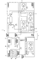
図1は、第1の実施の形態にかかる光電気混載集積回路の構成を示す図である。なお、本図は、主要構成部分の接続の様子を模式的に示している。本実施の形態にかかる光電気混載集積回路1は、演算部2、光配線部3、および、電源部(電源制御部)4を備えて構成されている。
(First embodiment)
FIG. 1 is a diagram illustrating a configuration of an opto-electric hybrid integrated circuit according to the first embodiment. In addition, this figure has shown typically the mode of the connection of the main components. The opto-electric hybrid integrated
演算部2は、演算処理を行い、主演算部5とスタンバイ・モード制御部6とを備えて構成されている。主演算部5は、通常のCMOS回路により構成され、光電気混載集積回路1に要求される実際の演算処理を行い、スタンバイ・モード制御部6へ後述するスタンバイ信号(STB)を送信し、図示されていない入出力部を介して外部と情報の交換を行う。
The
ここで、主演算部5は、個々に演算処理を行う第1の演算ブロック7、第2の演算ブロック8、第3の演算ブロック9、および、スタンバイ信号生成部10を備えて構成されている。そして、第1の演算ブロック7と第2の演算ブロック8とは、光配線部3を介して接続され、第1の演算ブロック7で計算された演算結果が、光配線部3を経由して、第2の演算ブロック8へ伝達される構成となっている。なお、第3の演算ブロック9は、光配線部3とは直接接続されておらず、全て電気配線により構成されている。
Here, the
スタンバイ信号生成部10は、スタンバイ・モード(待機状態)に入ることを指示するスタンバイ信号(STB)を生成する。ここで、スタンバイ・モードとは、光配線部3と主演算部5とが停止し、スタンバイ・モード制御部6のみが稼動している状態、すなわち、後述する光源用電源部17と主演算部用電源部15とが停止し、スタンバイ・モード制御部用電源部16のみが稼動している状態をいう。従って、スタンバイ・モードでは、消費電力が大幅に低下している状態となる。
The
スタンバイ信号(STB)は、主演算部5にある全ての演算ブロックが演算処理を休止している状態である場合に生成される。具体的には、スタンバイ信号生成部10が、主演算部5にある第1の演算ブロック7、第2の演算ブロック8、および、第3の演算ブロック9から、各演算ブロックが実質的に演算処理を休止している状態であることを示す信号(IDL)を反転論理で受け取り、OR演算処理を行うことにより、スタンバイ信号(STB)を生成している。なお、スタンバイ信号生成部10は、スタンバイ信号(STB)を反転論理で作成しているが、その理由は、後ほど詳しく説明する。
The standby signal (STB) is generated when all the arithmetic blocks in the main
スタンバイ・モード制御部6は、光電気混載集積回路1におけるスタンバイ・モードを制御する。具体的には、電源部4にスタンバイ信号(STB)またはスタンバイ解除信号を送信することにより、後述する光源用電源部17と主演算部用電源部15のオンおよびオフ、即ち、光配線部3と主演算部5とへの電力供給を制御する。スタンバイ・モード制御部6は、通常のCMOS回路により構成され、光配線への直接の接続は無く、全て電気配線のみにより構成されている。したがって、光配線部2の後述する発光素子12が停止している状態でも、その機能を保つことが可能である。スタンバイ・モード制御部6の機能については、後ほど詳しく説明する。
The standby
光配線部3は、主演算部5に配置された第1の演算ブロック7と第2の演算ブロック8とに接続され、第1の演算ブロック7での演算結果である電気信号を光信号に変換し、光信号で伝達後、再び電気信号に変換し、第2の演算ブロック8へ伝達する。光配線部3は、発光素子駆動部11、発光素子12、光導波路13、および、受光素子14を備えて構成されている。
The
発光素子駆動部11は、第1の演算ブロック7での演算結果である電気信号から発光素子12を駆動する。この発光素子駆動部11は、NMOSFETからなる。発光素子12は、光を発光し、第1の演算ブロック7での演算結果である電気信号を光信号に変換する。この発光素子12は、GaInNAs半導体レーザーからなる。なお、発光素子12の定格電流は0.7mAであり、必要な電源電圧は1.5Vなので、発光素子12の点灯時の消費電力は1.05mWである。この消費電力は、演算部2の待機状態での消費電力と比べてはるかに大きい。
The light emitting
ここで、発光素子駆動部11が発光素子12を駆動し、発光素子12が発光することにより、第1の演算ブロック7での演算結果である電気信号が光信号に変換される仕組みを簡単に説明する。第1の演算ブロック7での演算結果である電気信号が、発光素子駆動部11に伝達されると、発光素子駆動部11のNMOSFETがオンとオフを繰り返す。そして、NMOSFETがオンの時には、発光素子12に電流が流れるため発光素子12が発光し、NMOSFETがオフの時には、発光素子12に電流が流れないため発光素子12が発光しない。この発光素子12による光の点滅が光信号となり、電気信号が光信号に変換される。
Here, the light emitting
光導波路13は、発光素子12と受光素子14とを接続し、発光素子12による光信号を受光素子14へ伝達する。この光導波路13は、シリコン(Si)からなる。受光素子14は、光を受光すると光の強度に応じた電気を発生させる。従って、光導波路13を通って伝達された光信号を、第1の演算ブロック7での演算結果である電気信号へ再び変換し、第3の演算ブロック9へ伝達する。この受光素子14は、InGaAsフォトダイオードからなる。
The
電源部4は、演算部2と光配線部3とに、電力を供給する。電源部4は、主演算部用電源部15、スタンバイ・モード制御部用電源部16、光源用電源部17、(ブートアップ)シーケンサー18、第1のスイッチング素子19、および、第2のスイッチング素子20を備えて構成されている。
The
主演算部用電源部15は、主演算部5へ電力を供給する。スタンバイ・モード制御部用電源部16は、スタンバイ・モード制御部6へ電力を供給する。光源用電源部17は、光配線部3(発光素子12)へ電力を供給する。
The main calculation unit
なお、演算部2(主演算部5およびスタンバイ・モード制御部6)の必要とする電源電圧は、1.0Vであるのに対し、光配線部3の発光素子12が必要な電源電圧は、前述したように1.5Vである。従って、電源部4は、二つの異なる出力電圧を供給し、これらの電圧は、共通の入力電圧から、いわゆるDC−DCコンバーターにより生成されている。
The power supply voltage required by the calculation unit 2 (the
シーケンサー18は、起動時には、ブートアップシーケンサーとして機能し、系の初期化動作を行う。また、シーケンサー18は、スタンバイ・モードからの復帰時には、電源部4の各部の出力を再開する順序の制御を行う。
The
第1のスイッチング素子19は、スタンバイ信号(STB)およびスタンバイ解除信号に基づき、主演算部用電源部15への電力の供給および遮断を切り替える。この第1のスイッチング素子19は、電源部4内部にある制御回路であり、主演算部用電源部15の入力側に配置されている。第2のスイッチング素子20は、スタンバイ信号(STB)およびスタンバイ解除信号に基づき、光源用電源部17への電力の供給および遮断を切り替える。この第2のスイッチング素子20は、電源部4内部にある制御回路であり、光源用電源部17の入力側に配置されている。
The
なお、第1のスイッチング素子19および第2のスイッチング素子20は、主演算部用電源部15および光源用電源部17の出力側に配置することも可能であるが、入力側に配置した方が、DC−DCコンバーターを含む電源部4自身が消費する電力を、さらに削減することが可能なので、より望ましい構成となる。
The
また、電源部4自身の消費する電力には、定電圧化の処理のために必要な電力が含まれており、その値は実際の出力電流だけでなく、出力可能な最大出力電流にも依存する。従って、消費電力を低下させるためには、最大出力電流の大きな電源への電源入力を切断することが有効である。
In addition, the power consumed by the
(スタンバイ・モード制御)
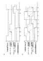
ここで、スタンバイ・モード制御部6によるスタンバイ・モード制御の仕組みについて、詳しく説明する。図2は、スタンバイ・モード制御のタイミングチャートである。なお、図2の(a)は、本実施の形態で実際に使用されるスタンバイ・モード制御のタイミングチャートである。
(Standby mode control)
Here, the mechanism of standby mode control by the standby
スタンバイ・モード制御部6は、主演算部5からスタンバイ信号(STB)を受信すると((a)の時刻A)、最終的にスタンバイ・モードに入るか否かの判定を行う。なお、スタンバイ・モード制御部6は、図示されていない入出力部からスタンバイ信号(STB)を受信した場合でも、同様の判定を行う。そして、スタンバイ・モード制御部6がスタンバイ・モードに入ると判定した場合には、電源部4にスタンバイ信号(STB)を送信する((a)の時刻B)。
When the standby
電源部4は、スタンバイ信号(STB)を受け取ると、第2のスイッチング素子20と第1のスイッチング素子19とをオフにすることにより、光源用電源部17と主演算部用電源部15とへの電力供給を切断し((a)の時刻C)、その後、光電気混載集積回路1は、スタンバイ・モードで動作する。この結果、光電気混載集積回路1の消費電力は、大幅に低下する。
When the
光電気混載集積回路1がスタンバイ・モードで動作中も、スタンバイ・モード制御部6には、スタンバイ・モード制御部用電源部16から電力が供給され続け、スタンバイ・モードの制御を行うことが可能である。例えば、光電気混載集積回路1がスタンバイ・モードで動作中に、図示されていない入出力部を介して外部からの動作状態の問い合わせ信号が入った場合、スタンバイ・モード制御部6は、光電気混載集積回路1がスタンバイ・モードであると連絡する信号を返信する制御を行うことができる。
Even when the opto-electric hybrid
なお、スタンバイ・モード制御部6は、スタンバイ・モードで動作中は、外部からの問い合わせの有無に関わらず、常にスタンバイ・モードであると連絡する信号を発信し続けることも可能であるが、信号を発信し続けることは消費電力の増加を招くので、望ましくは、前述の形態とした方がよい。
While the standby
光電気混載集積回路1がスタンバイ・モードで動作中に、スタンバイ・モード制御部6は、図示されていない入出力部または主演算部5からスタンバイ・モードの解除を指示するスタンバイ解除信号を受信すると((a)の時刻D)、電源部4にスタンバイ解除信号を送信する((a)の時刻E)。
When the opto-electric hybrid
電源部4は、スタンバイ解除信号を受け取ると、シーケンサー18の指示に基づき、第2のスイッチング素子20と第1のスイッチング素子19とをオンにすることにより、光源用電源部17と主演算部用電源部15とへの電力供給を順次再開し((a)の時刻E)、光配線部3を使用した主演算部5の機能が有効となる。そして、主演算部5は、電力供給の再開を受けて、内部メモリ状態の確認等の初期化処理を行い、入出力部からの信号処理の指示が受信可能となる。こうして、光電気混載集積回路1は、通常の状態で動作する。
When the
このように、主演算部の演算処理状態に応じて、通常の稼働状態と、スタンバイ・モードでの稼働状態とを適宜切り替えることにより、光電気混載集積回路1は、正常な演算処理を行いながら、電力を効率的に消費することができ、結果的に消費電力を大幅に低下することが可能となる。
As described above, the opto-electric hybrid
本実施の形態では、スタンバイ・モード制御部6は、主演算部5からのスタンバイ信号(STB)を反転論理で受信している。すなわち、スタンバイ信号生成部10が、スタンバイ信号(STB)を反転論理で作成している。このように構成することにより、光電気混載集積回路1がスタンバイ・モードに入り、主演算部5への電力供給が停止した時に、主演算部5から出力される信号が全て0Vとなり、主演算部5からのスタンバイ信号(STB)が、見かけ上反転してしまう事態を防ぐことができる。この理由を、図2の(b)を使用して説明する。
In the present embodiment, the standby
図2の(b)は、スタンバイ・モード制御部6が、主演算部5からのスタンバイ信号(STB)を反転論理で受信しなかった場合のスタンバイ・モード制御のタイミングチャートである。スタンバイ・モード制御部6が、主演算部5からスタンバイ信号(STB)を受信し((b)の時刻A)、スタンバイ・モードに入ると判定した場合には、電源部4にスタンバイ信号(STB)を送信する((b)の時刻B)。電源部4は、スタンバイ信号(STB)を受け取ると、光源用電源部17と主演算部用電源部15とへの電力供給を切断し((a)の時刻C)、その後、光電気混載集積回路1は、スタンバイ・モードで動作する。
FIG. 2B is a timing chart of standby mode control in the case where the standby
ところが、電力供給を切断された主演算部5は、スタンバイ信号(STB)を維持することができず、自動的に0V(Lレベル)を出力してしまう((b)の時刻C)。すると、スタンバイ・モード制御部6は、スタンバイ信号(STB)が反転したと受け取り、電源部4にスタンバイ解除信号を出力する((b)の時刻D)。この結果、光源用電源部17と主演算部用電源部15とは電力の供給を再開し、電力の供給再開とともに、主演算部5によりスタンバイ信号(STB)が再度出力される(Hレベルになる)((b)の時刻E)。従って、時刻Eの状態は、時刻Aの状態と同じとなり、系は自動的に同じ動作を繰り返す結果((b)の時刻E〜H)、発振状態に陥り、スタンバイ・モードでの動作を維持することが不可能となってしまう。
However, the
この問題を回避するために、スタンバイ・モード制御部6が、主演算部5からのスタンバイ信号(STB)のうち立ち上がり部分(スタンバイ状態に入る場合)のみを利用し、立ち下がり部分(スタンバイ状態から復帰する場合)は無視するように、スタンバイ・モード制御部6の演算回路を設計する手法も可能である。しかし、このような演算回路に必要な面積は、反転論理を用いる場合はNOT回路を一個追加するのみで済むことと比較すると、はるかに大きい。
In order to avoid this problem, the standby
このように、反転論理を用いてシステム設計を行うことにより、主演算部5からスタンバイ・モード制御部6へのスタンバイ・モード移行の指示を、簡単な回路設計で、確実に行うことが可能となる。
In this way, by designing the system using inversion logic, it is possible to reliably instruct the standby mode transition from the main
(発光素子駆動方法)
発光素子駆動部が発光素子を駆動する方法は、図1に示した方法以外にも、他の方法を利用することも可能である。図3は、発光素子駆動部が発光素子を駆動する他の方法を示した図である。図1に示した方法は、発光素子駆動部11であるNMOSFETが電流調整用の抵抗器の役割も兼ねることが出来るので、構成が最も単純であるが、0.7mAという比較的大きな電流を高速でスイッチするため、電源線や接地線にノイズが入る可能性が高いという問題がある。このため、設計の際には、電源線や接地線の配置等に注意が必要であり、設計への制約が発生する。
(Light emitting element driving method)
In addition to the method shown in FIG. 1, other methods can be used as the method for driving the light emitting element by the light emitting element driving unit. FIG. 3 is a diagram illustrating another method in which the light emitting element driving unit drives the light emitting element. The method shown in FIG. 1 has the simplest configuration because the NMOSFET that is the light emitting
これに対し、図3の(a)に示す方法では、発光素子駆動部22は、NMOSFET、PMOSFET、および、抵抗により構成されている。この構成では、発光素子12に電流が流れない時には並列の抵抗負荷に電流が流れるため、電源線や接地線を流れる電流の時間変動が極めて小さくなる利点がある。そして、この場合には、制御信号のオン/オフに関わらずどちらかの負荷に電流が流れるため、低消費電力化のためには、光配線部3を使用しないスタンバイ・モードにおいて光源用電源部17の電力供給を停止することが極めて有効になる。
On the other hand, in the method shown in FIG. 3A, the light emitting element driving unit 22 is composed of an NMOSFET, a PMOSFET, and a resistor. With this configuration, when no current flows through the
しかしながら、図1や図3の(a)に示した方法では、発光素子の駆動に用いられるNMOSFETの電流駆動力として、発光素子12を流れる電流と同じ(あるいは、同程度の)大きさの電流値が必要となる。これに対して、図3の(b)に示す方法では、発光素子駆動部23は、NMOSFETおよび抵抗により構成されている。この構成では、NMOSFETがオフ状態の際に、発光素子のレーザー発振閾値を1〜2割程度上回る電流が流れる様に直列の抵抗値を設定しておけば、NMOSFETの電流駆動力は発光素子を流れる電流の2〜3割程度で十分に制御可能となる。
However, in the method shown in FIG. 1 and FIG. 3A, the current driving force of the NMOSFET used for driving the light emitting element is a current having the same magnitude (or the same level) as the current flowing through the
MOSFETは電流駆動力が小さくて構わなければ、素子寸法も小さくすることが可能であり設計も容易になるため、低コスト化を図ることができる利点がある。この場合にも、制御信号のオン/オフに関わらずある程度の電流が流れる構成となるため、低消費電力化のためには、光配線部3を使用しないスタンバイ・モードにおいて光源用電源部17の電力供給を停止することが極めて有効になる。
As long as the current driving capability of the MOSFET is small, the element size can be reduced and the design can be facilitated. Therefore, there is an advantage that the cost can be reduced. Also in this case, since a certain amount of current flows regardless of whether the control signal is on or off, in order to reduce power consumption, the light source
このように、第1の実施の形態にかかる光電気混載集積回路によれば、消費電力の大きな発光素子を有する光配線部への電力供給と、この光配線を用いて信号伝達を行う主演算部への電力供給とを遮断したスタンバイ・モードを設けることにより、回路の正常な動作を保証しながら消費電力を大幅に低下させる光電気混載集積回路を提供することが可能である。この結果、携帯機器に代表される、待機状態での低消費電力化が重要となる機器に搭載される光電気混載集積回路において、光配線の利益を享受することが可能となる。 Thus, according to the opto-electric hybrid integrated circuit according to the first embodiment, the main operation for supplying power to the optical wiring unit having the light-emitting elements with large power consumption and transmitting signals using the optical wiring is performed. By providing a standby mode in which the power supply to the unit is cut off, it is possible to provide an opto-electric hybrid integrated circuit that significantly reduces power consumption while ensuring normal operation of the circuit. As a result, it is possible to enjoy the benefits of optical wiring in an opto-electric hybrid integrated circuit mounted on a device such as a portable device in which low power consumption is important in a standby state.
(第2の実施の形態)
第2の実施の形態では、第1の実施の形態と比べて、光配線部の構成が異なっている。第2の実施の形態について、添付図面を参照して説明する。本実施の形態にかかる光電気混載集積回路の構成について、第1の実施の形態と異なる部分を説明する。他の部分については第1の実施の形態と同様であるので、同一の符号が付された箇所については、上述した説明を参照し、ここでの説明を省略する。
(Second Embodiment)
In the second embodiment, the configuration of the optical wiring portion is different from that of the first embodiment. A second embodiment will be described with reference to the accompanying drawings. Regarding the configuration of the opto-electric hybrid integrated circuit according to the present embodiment, a portion different from the first embodiment will be described. The other parts are the same as those in the first embodiment, and therefore, the parts having the same reference numerals are referred to the above description, and the description thereof is omitted here.
図4は、第2の実施の形態にかかる光電気混載集積回路の構成を示す図である。なお、本図は、主要構成部分の接続の様子を模式的に示している。本実施の形態にかかる光電気混載集積回路31は、演算部32、光配線部33、および、電源部(電源制御部)34を備えて構成されている。
FIG. 4 is a diagram illustrating a configuration of an opto-electric hybrid integrated circuit according to the second embodiment. In addition, this figure has shown typically the mode of the connection of the main components. The opto-electric hybrid
演算部32は、演算処理を行い、主演算部5とスタンバイ・モード制御部35とを備えて構成されている。ここで、主演算部5は、個々に演算処理を行う第1の演算ブロック7、第2の演算ブロック8、第3の演算ブロック9、および、スタンバイ信号生成部10を備えて構成されている。
The
スタンバイ信号生成部10は、スタンバイ・モード(待機状態)に入ることを指示するスタンバイ信号(STB)を生成する。ここで、スタンバイ・モードとは、光配線部33と主演算部5とが停止し、スタンバイ・モード制御部35のみが稼動している状態、すなわち、後述する光系用電源部38と主演算部用電源部15とが停止し、スタンバイ・モード制御部用電源部16のみが稼動している状態をいう。従って、スタンバイ・モードでは、消費電力が大幅に低下している状態となる。
The
スタンバイ・モード制御部35は、光電気混載集積回路31におけるスタンバイ・モードを制御する。具体的には、電源部34にスタンバイ信号(STB)またはスタンバイ解除信号を送信することにより、後述する光系用電源部38と主演算部用電源部15のオンおよびオフ、即ち、光配線部33と主演算部5とへの電力供給を制御する。スタンバイ・モード制御部35は、通常のCMOS回路により構成され、光配線への直接の接続は無く、全て電気配線のみにより構成されている。したがって、光配線部33の後述する発光素子12が停止している状態でも、その機能を保つことが可能である。基本的には、スタンバイ・モード制御部35の機能は、第1の実施の形態で説明したスタンバイ・モード制御部6の機能と同じであるので、詳しい説明は省略する。
The standby
光配線部33は、主演算部5に配置された第1の演算ブロック7と第2の演算ブロック8とに接続され、第1の演算ブロック7での演算結果である電気信号を光信号に変換し、光信号で伝達後、再び電気信号に変換し、第2の演算ブロック8へ伝達する。光配線部33は、発光素子12、光変調器変調部36、光変調器37、光導波路13、および、受光素子14を備えて構成されている。
The
発光素子12は、光を発光する。この発光素子12は、GaInNAs半導体レーザーからなる。なお、本実施の形態では、発光素子12は、光配線を使用している時には、常時点灯した状態である。なお、発光素子12の定格電流は0.7mAであり、必要な電源電圧は1.5Vなので、発光素子12の点灯時の消費電力は1.05mWである。この消費電力は、演算部32の待機状態での消費電力と比べてはるかに大きい。
The
光変調器変調部36は、第1の演算ブロック7での演算結果である電気信号に応じて光変調器37を変調する。この光変調器変調部36は、NMOSFETからなる。
The optical
光変調器37は、光導波路13を伝播する光の強度を変化させ、第1の演算ブロック7での演算結果である電気信号を光信号に変換する。この光変調器37は、ニオブ酸リチウムからなる。なお、光変調器37の駆動電圧も1.5Vとなるように設計されている。
The
ここで、光変調器変調部36が光変調器37を変調し、光変調器37が発光素子12の発光した光の強度を変化させることにより、第1の演算ブロック7での演算結果である電気信号が光信号に変換される仕組みを簡単に説明する。第1の演算ブロック7での演算結果である電気信号が、光変調器変調部36に伝達されると、光変調器変調部36のNMOSFETがオンとオフを繰り返し、この結果、光変調器37に印加される電圧が変化する。そして、常時点灯中の発光素子12の発光した光が光変調器37を通過すると、光変調器37に印加された電圧の変化に対応して光の強度も変化し、受光素子14が受ける光の強度も変化する。この光の強弱が光信号となり、電気信号が光信号に変換される。
Here, the optical
電源部34は、演算部32と光配線部33とに、電力を供給する。電源部34は、主演算部用電源部15、スタンバイ・モード制御部用電源部16、光系用電源部38、(ブートアップ)シーケンサー18、第1のスイッチング素子19、および、第2のスイッチング素子39を備えて構成されている。
The
光系用電源部38は、光配線部33(発光素子12および光変調器37)へ電力を供給する。なお、演算部32(主演算部5およびスタンバイ・モード制御部35)の必要とする電源電圧は、1.0Vであるのに対し、光配線部33の発光素子12および光変調器37が必要な電源電圧は、前述したように1.5Vである。従って、電源部34は、二つの異なる出力電圧を供給し、これらの電圧は、共通の入力電圧から、いわゆるDC−DCコンバーターにより生成されている。
The optical
第2のスイッチング素子39は、スタンバイ信号(STB)およびスタンバイ解除信号に基づき、光系用電源部38への電力の供給および遮断を切り替える。この第2のスイッチング素子39は、電源部34内部にある制御回路であり、光系用電源部38の入力側に配置されている。
The
なお、第1のスイッチング素子19および第2のスイッチング素子39は、主演算部用電源部15および光系用電源部38の出力側に配置することも可能であるが、入力側に配置した方が、DC−DCコンバーターを含む電源部34自身が消費する電力を、さらに削減することが可能なので、より望ましい構成となる。
The
また、電源部34自身の消費する電力には、定電圧化の処理のために必要な電力が含まれており、その値は実際の出力電流だけでなく、出力可能な最大出力電流にも依存する。従って、消費電力を低下させるためには、最大出力電流の大きな電源への電源入力を切断することが有効である。
In addition, the power consumed by the
このように、第2の実施の形態にかかる光電気混載集積回路によれば、消費電力の大きな発光素子と、光変調器とを有する光配線部への電力供給と、この光配線を用いて信号伝達を行う主演算部への電力供給とを遮断したスタンバイ・モードを設けることにより、回路の正常な動作を保証しながら消費電力を大幅に低下させる光電気混載集積回路を提供することが可能である。この結果、携帯機器に代表される、待機状態での低消費電力化が重要となる機器に搭載される光電気混載集積回路において、光配線の利益を享受することが可能となる。 As described above, according to the opto-electric hybrid integrated circuit according to the second embodiment, power is supplied to the optical wiring unit having the light-emitting element with high power consumption and the optical modulator, and the optical wiring is used. By providing a standby mode that cuts off the power supply to the main processing unit that performs signal transmission, it is possible to provide an opto-electric hybrid integrated circuit that greatly reduces power consumption while guaranteeing normal operation of the circuit It is. As a result, it is possible to enjoy the benefits of optical wiring in an opto-electric hybrid integrated circuit mounted on a device such as a portable device in which low power consumption is important in a standby state.
(第3の実施形態)
第3の実施の形態では、第1および第2の実施の形態と比べて、光配線部の入出力の対応が、1対1ではなく2対2で表されている点と、スタンバイ・モード制御部が、電源部だけでなく主演算部および光配線部の個々のユニットの電力供給スイッチを制御する機能を備えている点とが異なっている。第3の実施の形態について、添付図面を参照して説明する。
(Third embodiment)
In the third embodiment, as compared with the first and second embodiments, the correspondence between the input and output of the optical wiring section is expressed by 2 to 2 instead of 1 to 1, and the standby mode The control unit is different from the power control unit in that it has a function of controlling the power supply switch of each unit of the main calculation unit and the optical wiring unit. A third embodiment will be described with reference to the accompanying drawings.
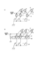
図5は、第3の実施の形態にかかる光電気混載集積回路の構成を示す図である。なお、本図は、主要構成部分の接続の様子を模式的に示している。本実施の形態にかかる光電気混載集積回路41は、演算部42、光配線部43、および、電源部(電源制御部)44を備えて構成されている。
FIG. 5 is a diagram showing a configuration of an opto-electric hybrid integrated circuit according to the third embodiment. In addition, this figure has shown typically the mode of the connection of the main components. The opto-electric hybrid
演算部42は、演算処理を行い、主演算部45およびスタンバイ・モード制御部46を備えて構成されている。主演算部45は、通常のCMOS回路により構成され、光電気混載集積回路41に要求される実際の演算処理を行い、スタンバイ・モード制御部46へ後述するスタンバイ信号(STB)を送信し、スタンバイ・モード制御部46との間で、後述する状態信号をやり取りし、図示されていない入出力部を介して外部と情報の交換を行う。
The
ここで、主演算部45は、個々に演算処理を行う第1の演算ブロック47、第2の演算ブロック48、第3の演算ブロック49、第4の演算ブロック50、第5の演算ブロック51、および、第1のスイッチ52、第2のスイッチ53、第3のスイッチ54、第4のスイッチ55、第5のスイッチ56、スタンバイ信号生成部57、および、状態信号生成部58を備えて構成されている。
Here, the
第1の演算ブロック47は、光配線部43を介して、第3の演算ブロック49および第4の演算ブロック50と接続され、第1の演算ブロック47で計算された演算結果が、光配線部43を経由して、第3の演算ブロック49および/または第4の演算ブロック50へ伝達される構成となっている。第2の演算ブロック48は、光配線部43を介して、第3の演算ブロック49および第4の演算ブロック50と接続され、第2の演算ブロック48で計算された演算結果が、光配線部43を経由して、第3の演算ブロック49および/または第4の演算ブロック50へ伝達される構成となっている。なお、第5の演算ブロック51は、光配線部43とは直接接続されておらず、全て電気配線により構成されている。
The
第1のスイッチ52は、後述する主演算部用電源部81と第1の演算ブロック47との間に設けられ、主演算部用電源部81から第1の演算ブロック47への電力の供給および遮断を切り替える。第2のスイッチ53は、後述する主演算部用電源部81と第2の演算ブロック48との間に設けられ、主演算部用電源部81から第2の演算ブロック48への電力の供給および遮断を切り替える。第3のスイッチ54は、後述する主演算部用電源部81と第3の演算ブロック49との間に設けられ、主演算部用電源部81から第3の演算ブロック49への電力の供給および遮断を切り替える。第4のスイッチ55は、後述する主演算部用電源部81と第4の演算ブロック50との間に設けられ、主演算部用電源部81から第4の演算ブロック50への電力の供給および遮断を切り替える。
The
第5のスイッチ56は、後述する主演算部用電源部81と第5の演算ブロック51との間に設けられ、主演算部用電源部81から第5の演算ブロック51への電力の供給および遮断を切り替える。なお、第1のスイッチ52、第2のスイッチ53、第3のスイッチ54、第4のスイッチ55、および、第5のスイッチ56のオンとオフの切り替えは、スタンバイ・モード制御部46からの指示により行われる。各スイッチの切り替え方法については、後ほどスタンバイ・モード制御部46による状態制御の説明とあわせて説明する。
The
スタンバイ信号生成部57は、スタンバイ・モード(待機状態)に入ることを指示するスタンバイ信号(STB)を生成する。ここで、スタンバイ・モードとは、光配線部43と主演算部45とが停止し、スタンバイ・モード制御部46のみが稼動している状態、すなわち、後述する光源用電源部83、光系用電源部84、および、主演算部用電源部81が停止し、スタンバイ・モード制御部用電源部82のみが稼動している状態をいう。従って、スタンバイ・モードでは、消費電力が大幅に低下している状態となる。
The
スタンバイ信号(STB)は、主演算部45にある全ての演算ブロックが演算処理を休止している状態である場合に生成される。具体的には、スタンバイ信号生成部57が、主演算部45にある第1の演算ブロック47、第2の演算ブロック48、第3の演算ブロック49、第4の演算ブロック50、第5の演算ブロック51から、各演算ブロックが実質的に演算処理を休止している状態であることを示す信号(IDL)を反転論理で受け取り、OR演算処理を行うことにより、スタンバイ信号(STB)を生成している。なお、スタンバイ信号生成部57は、スタンバイ信号(STB)を反転論理で作成しているが、その理由は、後ほど詳しく説明する。
The standby signal (STB) is generated when all the arithmetic blocks in the main
状態信号生成部58は、主演算部45の各部分の現在および今後の状態を表す状態信号を生成する。状態信号は、具体的には、主演算部45が行う演算処理に基づき、第1の演算ブロック47、第2の演算ブロック48、第3の演算ブロック49、第4の演算ブロック50、および、第5の演算ブロック51の現在の演算処理状態および今後の演算処理状態を表す。
The state
スタンバイ・モード制御部46は、光電気混載集積回路41におけるスタンバイ・モードを制御する。具体的には、電源部44にスタンバイ信号(STB)またはスタンバイ解除信号を送信することにより、後述する光源用電源部83、光系用電源部84、および、主演算部用電源部81のオンおよびオフ、即ち、光配線部43と主演算部45とへの電力供給を制御する。
The standby
さらに、スタンバイ・モード制御部46は、主演算部45にある各演算ブロックの状態と、光配線部43にある各受光素子および各光変調器の状態とを制御する。スタンバイ・モード制御部46は、具体的には、主演算部45からの状態信号に基づいて、主演算部45にある第1のスイッチ52、第2のスイッチ53、第3のスイッチ54、第4のスイッチ55、および、第4のスイッチ56をオンおよびオフすることにより、それぞれ、第1の演算ブロック47、第2の演算ブロック48、第3の演算ブロック49、第4の演算ブロック50、および、第5の演算ブロック51への電力供給を制御する。
Further, the standby
スタンバイ・モード制御部46は、さらに具体的には、主演算部45からの状態信号に基づいて、光配線部43にある、後述する第6のスイッチ75、第7のスイッチ76、第8のスイッチ77、および、第9のスイッチ78、第10のスイッチ79、および、第11のスイッチ80をオンおよびオフすることにより、それぞれ、後述する第1の発光素子59、第2の発光素子60、第1の光変調器65、第2の光変調器66、第3の光変調器67、および、第4の光変調器68への電力供給を制御する。
More specifically, the standby
スタンバイ・モード制御部46が、第1の光変調器65、第2の光変調器66、第3の光変調器67、および、第4の光変調器68への電力供給を制御することにより、主演算部45の各演算ブロック間のデータのやり取りを組み替えて、主演算部45を多機能回路として機能させることが可能である。
The standby
さらに、スタンバイ・モード制御部46が、第1の演算ブロック47、第2の演算ブロック48、第3の演算ブロック49、第4の演算ブロック50、第5の演算ブロック51、第1の発光素子59、および、第2の発光素子60への電力供給を制御することにより、光電気混載集積回路1の消費電力を大幅に低下させることが可能である。
Further, the standby
スタンバイ・モード制御部46は、通常のCMOS回路により構成され、光配線への直接の接続は無く、全て電気配線のみにより構成されている。したがって、光配線部43の後述する第1の発光素子59および第2の発光素子60が停止している状態でも、その機能を保つことが可能である。スタンバイ・モード制御部46のスタンバイ・モード制御機能および状態制御機能については、後ほど詳しく説明する。
The standby
光配線部43は、主演算部45に配置された第1の演算ブロック47、第2の演算ブロック48、第3の演算ブロック49、および、第4の演算ブロック50に接続され、第1の演算ブロック47での演算結果、および/または、第2の演算ブロック48での演算結果である電気信号を光信号に変換し光信号で伝達する。そして、第1の演算ブロック47での演算結果である光信号、および、第2の演算ブロック48での演算結果である光信号をそのまま、あるいは、第1の演算ブロック47での演算結果と第2の演算ブロック48での演算結果のOR信号である光信号を、再び電気信号に変換し、第3の演算ブロック49、および/または、第4の演算ブロック50へ伝達する。
The
光配線部43は、第1の発光素子59、第2の発光素子60、第1の光変調器変調部61、第2の光変調器変調部62、第3の光変調器変調部63、第4の光変調器変調部64、第1の光変調器65、第2の光変調器66、第3の光変調器67、第4の光変調器68、第1の光導波路69、第2の光導波路70、第3の光導波路71、第4の光導波路72、第1の受光素子73、第2の受光素子74、第6のスイッチ75、第7のスイッチ76、第8のスイッチ77、第9のスイッチ78、第10のスイッチ79、および、第11のスイッチ80を備えて構成されている。
The
第1の発光素子59および第2の発光素子60は、それぞれ光を発光する。第1の発光素子59および第2の発光素子60は、それぞれGaInNAs半導体レーザーからなる。本実施の形態では、第1の発光素子59および第2の発光素子60は、光配線を使用している時には、常時点灯した状態である。なお、後述するように、第1の光導波路69、第2の光導波路70、第3の光導波路71、および、第4の光導波路72が分岐を有する構成となっているため、第1の発光素子59および第2の発光素子60の定格電流は、それぞれ第1および第2の実施の形態よりも大きな1.0mAであり、必要な電源電圧は2.0Vとなっている。従って、第1の発光素子59および第2の発光素子60の点灯時の消費電力は、それぞれ2.0mWとなる。これらの消費電力は、演算部42の待機状態での消費電力と比べてはるかに大きい。
The first light emitting element 59 and the second light emitting element 60 each emit light. The first light emitting element 59 and the second light emitting element 60 are each composed of a GaInNAs semiconductor laser. In the present embodiment, the first light emitting element 59 and the second light emitting element 60 are always lit when the optical wiring is used. As will be described later, the first
第1の光変調器変調部61は、第1の演算ブロック47での演算結果である電気信号に応じて第1の光変調器65を変調する。第2の光変調器変調部62は、第1の演算ブロック47での演算結果である電気信号に応じて第2の光変調器66を変調する。第3の光変調器変調部63は、第2の演算ブロック48での演算結果である電気信号に応じて第3の光変調器67を変調する。第4の光変調器変調部64は、第2の演算ブロック48での演算結果である電気信号に応じて第4の光変調器68を変調する。第1の光変調器変調部61、第2の光変調器変調部62、第3の光変調器変調部63、および、第4の光変調器変調部64は、それぞれNMOSFETからなる。
The first optical
第1の光変調器65は、第1の光導波路69を伝播する光の強度を変化させ、第1の演算ブロック47での演算結果である電気信号を光信号に変換する。第2の光変調器66は、第2の光導波路70を伝播する光の強度を変化させ、第1の演算ブロック47での演算結果である電気信号を光信号に変換する。第3の光変調器67は、第3の光導波路71を伝播する光の強度を変化させ、第2の演算ブロック48での演算結果である電気信号を光信号に変換する。第4の光変調器68は、第4の光導波路72を伝播する光の強度を変化させ、第2の演算ブロック48での演算結果である電気信号を光信号に変換する。
The first
第1の光変調器65、第2の光変調器66、第3の光変調器67、および、第4の光変調器68は、それぞれニオブ酸リチウムからなる。第1の光変調器65、第2の光変調器66、第3の光変調器67、および、第4の光変調器68の駆動電圧は1.5Vとなるように設計されている。
The first
ここで、第1から第4の光変調器変調部がそれぞれ対応する第1から第4の光変調器を変調し、第1から第4の光変調器が第1および第2の発光素子の発光した光の強度を変化させることにより、第1および第2の演算ブロックでの演算結果である電気信号が光信号に変換される仕組みを、第1の演算ブロック47から第1の受光素子73までの信号の流れを用いて簡単に説明する。
Here, the first to fourth light modulator modulators respectively modulate the corresponding first to fourth light modulators, and the first to fourth light modulators respectively correspond to the first and second light emitting elements. By changing the intensity of the emitted light, an electrical signal that is the result of the calculation in the first and second calculation blocks is converted into an optical signal from the
第1の演算ブロック47での演算結果である電気信号が、第1の光変調器変調部61に伝達されると、第1の光変調器変調部61のNMOSFETがオンとオフを繰り返し、この結果、第1の光変調器65に印加される電圧が変化する。そして、常時点灯中の第1の発光素子59の発光した光が第1の光変調器65を通過すると、第1の光変調器65に印加された電圧の変化に対応して光の強度も変化し、第1の受光素子73が受ける光の強度も変化する。この光の強弱が光信号となり、電気信号が光信号に変換される。
When the electric signal as the calculation result in the
なお、本実施の形態においては、第1から第4の光変調器に電圧が印加されない状態で、第1から第4の光導波路を伝播する光の強度が小さくなり、第1から第4の光変調器4に電圧が印加された状態で、第1から第4の光導波路を伝播する光の強度が大きくなるように構成されている。
In the present embodiment, in the state where no voltage is applied to the first to fourth optical modulators, the intensity of light propagating through the first to fourth optical waveguides is reduced, and the first to fourth optical modulators are reduced. In the state where a voltage is applied to the
第1の光導波路69は、第1の発光素子59と第1の受光素子73とを接続し、第1の発光素子59による光信号を第1の受光素子73へ伝達する。より詳しくは、第1の光導波路69は、第1の発光素子59と接続されている一端が後述する第2の光導波路70と共通となっており、第2の光導波路70と分岐後、第1の光変調器65を経由し、さらに、後述する第3の光導波路71と合流後、他端が第1の受光素子73と接続されている構成となっている。
The first
第2の光導波路70は、第1の発光素子59と第2の受光素子74とを接続し、第1の発光素子59による光信号を第2の受光素子74へ伝達する。より詳しくは、第2の光導波路70は、第1の発光素子59と接続されている一端が前述の第1の光導波路69と共通となっており、第1の光導波路69と分岐後、第2の光変調器66を経由し、さらに、後述する第4の光導波路72と合流後、他端が第2の受光素子74と接続されている構成となっている。
The second
第3の光導波路71は、第2の発光素子60と第1の受光素子73とを接続し、第2の発光素子60による光信号を第1の受光素子73へ伝達する。より詳しくは、第3の光導波路71は、第2の発光素子60と接続されている一端が後述する第4の光導波路72と共通となっており、第4の光導波路72と分岐後、第3の光変調器67を経由し、さらに、前述の第1の光導波路69と合流後、他端が第1の受光素子73と接続されている構成となっている。
The third
第4の光導波路72は、第2の発光素子60と第2の受光素子74とを接続し、第2の発光素子60による光信号を第2の受光素子74へ伝達する。より詳しくは、第4の光導波路72は、第2の発光素子60と接続されている一端が前述の第3の光導波路71と共通となっており、第3の光導波路71と分岐後、第4の光変調器68を経由し、さらに、前述の第2の光導波路70と合流後、他端が第2の受光素子74と接続されている構成となっている。第1の光導波路69、第2の光導波路70、第3の光導波路71、および、第4の光導波路72は、それぞれシリコン(Si)からなる。
The fourth
上述したように、各々の光導波路が、それぞれ他の光導波路と分岐および合流する構成となっているため、光配線部43の入出力の対応が2対2となり、主演算部45の各演算ブロック間のデータを組み替えて、主演算部45を多機能回路として機能させることが可能である。各演算ブロック間のデータの組み替え方法については、後ほどスタンバイ・モード制御部46による状態制御の説明とあわせて説明する。
As described above, since each optical waveguide is configured to branch and merge with other optical waveguides, the input / output correspondence of the
第1の受光素子73は、光を受光すると光の強度に応じた電気を発生させる。従って、第1の受光素子73は、第1の光導波路69および/または第3の光導波路71を通って伝達された光信号を、電気信号へ再び変換し、第3の演算ブロック49へ伝達する。第2の受光素子74は、光を受光すると光の強度に応じた電気を発生させる。従って、第2の受光素子74は、第2の光導波路70および/または第4の光導波路72を通って伝達された光信号を、電気信号へ再び変換し、第4の演算ブロック50へ伝達する。第1の受光素子73および第2の受光素子74は、InGaAsフォトダイオードからなる。
When receiving the light, the first
第6のスイッチ75は、後述する光源用電源部83と第1の発光素子59との間に設けられ、光源用電源部83から第1の発光素子59への電力供給および遮断を切り替える。第7のスイッチ76は、後述する光源用電源部83と第2の発光素子60との間に設けられ、光源用電源部83から第2の発光素子60への電力供給および遮断を切り替える。
The
第8のスイッチ77は、後述する光系用電源部84と第1の光変調器65との間に設けられ、光系用電源部84から第1の光変調器65への電力供給および遮断を切り替える。第9のスイッチ78は、後述する光系用電源部84と第2の光変調器66との間に設けられ、光系用電源部84から第2の光変調器66への電力供給および遮断を切り替える。第10のスイッチ79は、後述する光系用電源部84と第3の光変調器67との間に設けられ、光系用電源部84から第3の光変調器67への電力供給および遮断を切り替える。第11のスイッチ80は、後述する光系用電源部84と第4の光変調器68との間に設けられ、光系用電源部84から第4の光変調器68への電力供給および遮断を切り替える。
The
なお、第6のスイッチ75、第7のスイッチ76、第8のスイッチ77、第9のスイッチ78、第10のスイッチ79、および、第11のスイッチ80のオンとオフの切り替えは、スタンバイ・モード制御部46からの指示により行われる。各スイッチの切り替え方法については、後ほどスタンバイ・モード制御部46による状態制御の説明とあわせて説明する。
The
電源部44は、演算部42と光配線部43とに、電力を供給する。電源部44は、主演算部用電源部81、スタンバイ・モード制御部用電源部82、光源用電源部83、光系用電源部84、(ブートアップ)シーケンサー85、第1のスイッチング素子86、第2のスイッチング素子87、および、第3のスイッチング素子88を備えて構成されている。
The
主演算部用電源部81は、主演算部45へ電力を供給する。スタンバイ・モード制御部用電源部82は、スタンバイ・モード制御部46へ電力を供給する。光源用電源部83は、光配線部43の第1の発光素子59および第2の発光素子60へ電力を供給する。光系用電源部84は、光配線部43の第1の光変調器65、第2の光変調器66、第3の光変調器67、および、第4の光変調器68へ電力を供給する。
The main arithmetic unit
なお、演算部42(主演算部45およびスタンバイ・モード制御部46)の必要とする電源電圧は、1.0Vである。それに対し、光配線部43の第1の発光素子59および第2の発光素子60が必要な電源電圧は、前述したように2.0Vであり、光配線部43の第1の光変調器65、第2の光変調器66、第3の光変調器67、および、第4の光変調器68が必要な電源電圧は、前述したように1.5Vである。従って、電源部44は、三つの異なる出力電圧を供給し、これらの電圧は、共通の入力電圧から、いわゆるDC−DCコンバーターにより生成されている。
The power supply voltage required by the calculation unit 42 (the
シーケンサー85は、起動時には、ブートアップシーケンサーとして機能し、系の初期化動作を行う。また、シーケンサー85は、スタンバイ・モードからの復帰時には、電源部44の各部の出力を再開する順序の制御を行う。
The
第1のスイッチング素子86は、スタンバイ信号(STB)およびスタンバイ解除信号に基づき、主演算部用電源部81への電力の供給および遮断を切り替える。この第1のスイッチング素子86は、電源部44内部にある制御回路であり、主演算部用電源部81の入力側に配置されている。第2のスイッチング素子87は、スタンバイ信号(STB)およびスタンバイ解除信号に基づき、光源用電源部83への電力の供給および遮断を切り替える。この第2のスイッチング素子87は、電源部44内部にある制御回路であり、光源用電源部83の入力側に配置されている。第3のスイッチング素子88は、スタンバイ信号(STB)およびスタンバイ解除信号に基づき、光系用電源部84への電力の供給および遮断を切り替える。この第3のスイッチング素子88は、電源部44内部にある制御回路であり、光系用電源部84の入力側に配置されている。
The
なお、第1のスイッチング素子86、第2のスイッチング素子87、および、第3のスイッチング素子88は、主演算部用電源部81、光源用電源部83、および、光系用電源部84の出力側に配置することも可能であるが、入力側に配置した方が、DC−DCコンバーターを含む電源部44自身が消費する電力を、さらに削減することが可能なので、より望ましい構成となる。
The
また、電源部44自身の消費する電力には、定電圧化の処理のために必要な電力が含まれており、その値は実際の出力電流だけでなく、出力可能な最大出力電流にも依存する。従って、消費電力を低下させるためには、最大出力電流の大きな電源への電源入力を切断することが有効である。
In addition, the power consumed by the
(スタンバイ・モード制御)
ここで、スタンバイ・モード制御部46によるスタンバイ・モード制御の仕組みについて、図2を使用して、詳しく説明する。スタンバイ・モード制御部46は、主演算部42からスタンバイ信号(STB)を受信すると((a)の時刻A)、最終的にスタンバイ・モードに入るか否かの判定を行う。なお、スタンバイ・モード制御部46は、図示されていない入出力部からスタンバイ信号(STB)を受信した場合でも、同様の判定を行う。
(Standby mode control)
Here, the mechanism of the standby mode control by the standby
そして、スタンバイ・モード制御部46がスタンバイ・モードに入ると判定した場合には、電源部44にスタンバイ信号(STB)を送信する((a)の時刻B)。電源部44は、スタンバイ信号(STB)を受け取ると、第2のスイッチング素子87、第3のスイッチング素子88、および、第1のスイッチング素子86をオフにすることにより、光源用電源部83、光系用電源部84、および、主演算部用電源部81への電力供給を切断し((a)の時刻C)、その後、光電気混載集積回路41は、スタンバイ・モードで動作する。この結果、光電気混載集積回路41の消費電力は、大幅に低下する。
When the standby
光電気混載集積回路41がスタンバイ・モードで動作中も、スタンバイ・モード制御部46には、スタンバイ・モード制御部用電源部82から電力が供給され続け、スタンバイ・モードの制御を行うことが可能である。例えば、光電気混載集積回路41がスタンバイ・モードで動作中に、図示されていない入出力部を介して外部からの動作状態の問い合わせ信号が入った場合、スタンバイ・モード制御部46は、光電気混載集積回路41がスタンバイ・モードであると連絡する信号を返信する制御を行うことができる。
Even when the opto-electric hybrid
なお、スタンバイ・モード制御部46は、スタンバイ・モードで動作中は、外部からの問い合わせの有無に関わらず、常にスタンバイ・モードであると連絡する信号を発信し続けることも可能であるが、信号を発信し続けることは消費電力の増加を招くので、望ましくは、前述の形態とした方がよい。
While the standby
光電気混載集積回路41がスタンバイ・モードで動作中に、スタンバイ・モード制御部46は、図示されていない入出力部または主演算部45からスタンバイ・モードの解除を指示するスタンバイ解除信号を受信すると((a)の時刻D)、電源部44にスタンバイ解除信号を送信する((a)の時刻E)。
When the opto-electric hybrid
電源部44は、スタンバイ解除信号を受け取ると、シーケンサー85の指示に基づき、第2のスイッチング素子87、第3のスイッチング素子88、および、第1のスイッチング素子86をオンにすることにより、光源用電源部83、光系用電源部84、および、主演算部用電源部81への電力供給を順次再開し((a)の時刻E)、光配線部43を使用した主演算部45の機能が有効となる。そして、主演算部45は、電力供給の再開を受けて、内部メモリ状態の確認等の初期化処理を行い、入出力部からの信号処理の指示が受信可能となる。こうして、光電気混載集積回路41は、通常の状態で動作する。
Upon receiving the standby release signal, the
このように、主演算部の演算処理状態に応じて、通常の稼働状態と、スタンバイ・モードでの稼働状態とを適宜切り替えることにより、光電気混載集積回路41は、正常な演算処理を行いながら、電力を効率的に消費することができ、結果的に消費電力を大幅に低下することが可能となる。
As described above, the opto-electric hybrid
本実施の形態では、スタンバイ・モード制御部46は、主演算部45からのスタンバイ信号(STB)を反転論理で受信している。すなわち、スタンバイ信号生成部57が、スタンバイ信号(STB)を反転論理で作成している。このように構成することにより、光電気混載集積回路41がスタンバイ・モードに入り、主演算部45への電力供給が停止した時に、主演算部45から出力される信号が全て0Vとなり、主演算部45からのスタンバイ信号(STB)が、見かけ上反転してしまう事態を防ぐことができる。この理由を、図2の(b)を使用して説明する。
In the present embodiment, the standby
図2の(b)は、スタンバイ・モード制御部46が、主演算部45からのスタンバイ信号(STB)を反転論理で受信しなかった場合のスタンバイ・モード制御のタイミングチャートである。スタンバイ・モード制御部46が、主演算部45からスタンバイ信号(STB)を受信し((b)の時刻A)、スタンバイ・モードに入ると判定した場合には、電源部44にスタンバイ信号(STB)を送信する((b)の時刻B)。電源部44は、スタンバイ信号(STB)を受け取ると、光源用電源部83、光系用電源部84、および、主演算部用電源部81への電力供給を切断し((a)の時刻C)、その後、光電気混載集積回路41は、スタンバイ・モードで動作する。
FIG. 2B is a timing chart of standby mode control when the standby
ところが、電力供給を切断された主演算部45は、スタンバイ信号(STB)を維持することができず、自動的に0V(Lレベル)を出力してしまう((b)の時刻C)。すると、スタンバイ・モード制御部46は、スタンバイ信号(STB)が反転したと受け取り、電源部44にスタンバイ解除信号を出力する((b)の時刻D)。この結果、光源用電源部83、光系用電源部84、および、主演算部用電源部81は電力の供給を再開し、電力の供給再開とともに、主演算部45によりスタンバイ信号(STB)が再度出力される(Hレベルになる)((b)の時刻E)。従って、時刻Eの状態は、時刻Aの状態と同じとなり、系は自動的に同じ動作を繰り返す結果((b)の時刻E〜H)、発振状態に陥り、スタンバイ・モードでの動作を維持することが不可能となってしまう。
However, the
この問題を回避するために、スタンバイ・モード制御部46が、主演算部45からのスタンバイ信号(STB)のうち立ち上がり部分(スタンバイ状態に入る場合)のみを利用し、立ち下がり部分(スタンバイ状態から復帰する場合)は無視するように、スタンバイ・モード制御部46の演算回路を設計する手法も可能である。しかし、このような演算回路に必要な面積は、反転論理を用いる場合はNOT回路を一個追加するのみで済むことと比較すると、はるかに大きい。
In order to avoid this problem, the standby
このように、反転論理を用いてシステム設計を行うことにより、主演算部45からスタンバイ・モード制御部46へのスタンバイ・モード移行の指示を、簡単な回路設計で、確実に行うことが可能となる。
In this way, by designing the system using inversion logic, it is possible to reliably instruct the standby mode transition from the main
(状態制御)
次に、スタンバイ・モード制御部46による状態制御の仕組みについて、再び図5を使用して、詳しく説明する。
(State control)
Next, the mechanism of state control by the standby
本実施の形態では、光配線部43の入出力の対応が2対2(光配線部43への入力部:第1の演算ブロック47および第2の演算ブロック48、光配線部43からの出力部:第3の演算ブロック49および第4の演算ブロック50)となっている。そして、スタンバイ・モード制御部46は、主演算部45からの状態信号に基づいて、光配線部43の各光変調器の電力供給スイッチを制御する機能を有している。このため、スタンバイ・モード制御部46は、主演算部45の各演算ブロック間のデータのやり取りを組み替えて、主演算部45を多機能回路として機能させることが可能である。以下に、その方法を説明する。
In the present embodiment, the input / output correspondence of the
スタンバイ・モード制御部46は、主演算部45からの状態信号に基づいて、第1の光変調器65への電力供給および遮断を切り替える第8のスイッチ77、および、第3の光変調器67への電力供給および遮断を切り替える第10のスイッチ79をオン/オフし、第3の演算ブロック49に入力されるデータを切り替える。第1の演算ブロック47からの出力データをA、第2の演算ブロック48からの出力データをB、第3の演算ブロック49への入力データをCとすると、以下の関係が成り立つ。
1.C=A+B(第1の光変調器65:オン、第3の光変調器67:オンの時)
2.C=A (第1の光変調器65:オン、第3の光変調器67:オフの時)
3.C=B (第1の光変調器65:オフ、第3の光変調器67:オンの時)
4.C=0 (第1の光変調器65:オフ、第3の光変調器67:オフの時)
The standby
1. C = A + B (when the first
2. C = A (when the first
3. C = B (when the first
4). C = 0 (when the first
また、スタンバイ・モード制御部46は、主演算部45からの状態信号に基づいて、第2の光変調器66への電力供給および遮断を切り替える第9のスイッチ78、および、第4の光変調器68への電力供給および遮断を切り替える第11のスイッチ80をオン/オフし、第4の演算ブロック50に入力されるデータを切り替える。さらに、第4の演算ブロック50の入力をDとすると、以下の関係が成り立つ。
1.D=A+B(第2の光変調器66:オン、第4の光変調器68:オンの時)
2.D=A (第2の光変調器66:オン、第4の光変調器68:オフの時)
3.D=B (第2の光変調器66:オフ、第4の光変調器68:オンの時)
3.D=0 (第2の光変調器66:オフ、第4の光変調器68:オフの時)
Further, the standby
1. D = A + B (when the second
2. D = A (when the second
3. D = B (when the second
3. D = 0 (when the second
例えば、C=A、D=Bとしたい場合、スタンバイ・モード制御部46は、その旨の状態信号を受け取ると、第8のスイッチ77をオン、第9のスイッチ78をオフ、第10のスイッチ79をオフ、第11のスイッチ80をオンする。また、C=B、D=Aとしたい場合、スタンバイ・モード制御部46は、その旨の状態信号を受け取ると、第8のスイッチ77をオフ、第9のスイッチ78をオン、第10のスイッチ79をオン、第11のスイッチ80をオフする。
For example, when it is desired to set C = A and D = B, when the standby
このように、スタンバイ・モード制御部46は、主演算部45からの状態信号に基づいて、第1の光変調器65、第2の光変調器66、第3の光変調器67、および、第4の光変調器68への電力供給を制御し、光配線部43から出力されるデータ(第3の演算ブロック49および第4の演算ブロック50へ入力されるデータ)を適宜切り替えることができる。このような切り替えを演算部の多数のブロック間で行うことにより、回路の機能を動的に組み替えつつ情報処理を行うことが可能となるので、回路の効率を向上させることが可能となる。
As described above, the standby
さらに、スタンバイ・モード制御部46は、主演算部45からの状態信号に基づいて、主演算部45の各演算ブロックの電力供給スイッチ、および、光配線部43の各発光素子の電力供給スイッチを制御する機能を有している。このため、スタンバイ・モード制御部46は、上記回路機能の組み替えで、一時的に不要となった部分の電力供給を停止させることが可能である。以下に、その方法を説明する。
Further, the standby
スタンバイ・モード制御部46は、主演算部45からの状態信号に基づいて、第1の演算ブロック47への電力の供給および遮断を切り替える第1のスイッチ52、第2の演算ブロック48への電力の供給および遮断を切り替える第2のスイッチ53、第3の演算ブロック49への電力の供給および遮断を切り替える第3のスイッチ54、第4の演算ブロック50への電力の供給および遮断を切り替える第4のスイッチ55、第1の発光素子59への電力供給および遮断を切り替える第6のスイッチ75、および、第2の発光素子60への電力供給および遮断を切り替える第7のスイッチ76をオン/オフする。
The standby
例えば、C=0かつD=Bの場合、第1の光変調器65、第2の光変調器66、および、第3の光変調器67はオフであり、第4の光変調器68のみがオンとなっている。この時、データが入力されていない第1の発光素子59をオフにすることが可能であり、さらに、データを出力しない、すなわち、演算処理を行っていない第1の演算ブロック47と、データを入力しない、すなわち、演算処理を行う予定のない第3の演算ブロック49とを、オフにすることが可能である。
For example, when C = 0 and D = B, the first
従って、スタンバイ・モード制御部46は、その旨の状態信号を受け取ると、第6のスイッチ75、第1のスイッチ52、および、第3のスイッチ54をオフする。このようなスイッチの切り替えを行うことにより、光電気混載集積回路41は、回路の演算機能を損なうことなく、電力を効率的に消費することができ、結果的に消費電力を大幅に低下することが可能となる。
Therefore, the standby
このように、第3の実施の形態にかかる光電気混載集積回路によれば、消費電力の大きな発光素子を有する光配線部への電力供給と、この光配線を用いて信号伝達を行う主演算部への電力供給とを遮断したスタンバイ・モードを設けることにより、回路の正常な動作を保証しながら消費電力を大幅に低下させる光電気混載集積回路を提供することが可能である。この結果、携帯機器に代表される、待機状態での低消費電力化が重要となる機器に搭載される光電気混載集積回路において、光配線の利益を享受することが可能となる。 As described above, according to the opto-electric hybrid integrated circuit according to the third embodiment, the main operation for supplying power to the optical wiring unit having the light-emitting elements with large power consumption and transmitting signals using the optical wiring is performed. By providing a standby mode in which the power supply to the unit is cut off, it is possible to provide an opto-electric hybrid integrated circuit that significantly reduces power consumption while ensuring normal operation of the circuit. As a result, it is possible to enjoy the benefits of optical wiring in an opto-electric hybrid integrated circuit mounted on a device such as a portable device in which low power consumption is important in a standby state.
さらに、第3の実施の形態にかかる光電気混載集積回路によれば、光配線部の各部分と主演算部の各部分とへの電力供給の開始および遮断を適宜行うことにより、回路の正常な動作を保証しながら消費電力を大幅に低下させる光電気混載集積回路を提供することが可能である。この結果、携帯機器に代表される、稼働不要な電力消費部分の停止による低消費電力化が重要となる機器に搭載される光電気混載集積回路において、光配線の利益を享受することが可能となる。 Furthermore, according to the opto-electric hybrid integrated circuit according to the third embodiment, the normal operation of the circuit is achieved by appropriately starting and shutting off the power supply to each part of the optical wiring part and each part of the main arithmetic part. It is possible to provide an opto-electric hybrid integrated circuit that greatly reduces power consumption while guaranteeing proper operation. As a result, it is possible to enjoy the benefits of optical wiring in an opto-electric hybrid integrated circuit that is installed in devices such as portable devices where low power consumption is important by stopping unnecessary power consumption. Become.
(第4の実施形態)
第4の実施の形態では、第1および第2の実施の形態と比べて、光配線部の入出力の対応が、1対1ではなく2対2で表されている点と、スタンバイ・モード制御部が、電源部だけでなく主演算部および光配線部の個々のユニットの電力供給スイッチを制御する機能を備えている点とが異なっている。さらに、第3の実施の形態では、発光素子と光配線への電気信号を出力する演算ブロックとが1対1で対応していたが、本実施の形態では、発光素子と光配線からの電気信号を入力する演算ブロックとが1対1で対応している。
(Fourth embodiment)
In the fourth embodiment, compared with the first and second embodiments, the input / output correspondence of the optical wiring section is expressed by 2 to 2 instead of 1 to 1, and the standby mode The control unit is different from the power control unit in that it has a function of controlling the power supply switch of each unit of the main calculation unit and the optical wiring unit. Furthermore, in the third embodiment, there is a one-to-one correspondence between the light emitting element and the calculation block that outputs an electrical signal to the optical wiring. There is a one-to-one correspondence with a calculation block for inputting a signal.
第4の実施の形態について、添付図面を参照して説明する。本実施の形態にかかる光電気混載集積回路の構成について、第3の実施の形態と異なる部分を説明する。他の部分については第3の実施の形態と同様であるので、同一の符号が付された箇所については、上述した説明を参照し、ここでの説明を省略する。 A fourth embodiment will be described with reference to the accompanying drawings. Regarding the configuration of the opto-electric hybrid integrated circuit according to the present embodiment, a different part from the third embodiment will be described. The other parts are the same as those in the third embodiment, and therefore, the portions having the same reference numerals are referred to the above description, and the description thereof is omitted here.
図6は、第4の実施の形態にかかる光電気混載集積回路の構成を示す図である。なお、本図は、主要構成部分の接続の様子を模式的に示している。本実施の形態にかかる光電気混載集積回路91は、演算部42、光配線部92、および、電源部(電源制御部)44を備えて構成されている。
FIG. 6 is a diagram illustrating a configuration of an opto-electric hybrid integrated circuit according to the fourth embodiment. In addition, this figure has shown typically the mode of the connection of the main components. The opto-electric hybrid
演算部42は、主演算部45およびスタンバイ・モード制御部46を備えて構成されている。ここで、主演算部45は、個々に演算処理を行う第1の演算ブロック47、第2の演算ブロック48、第3の演算ブロック49、第4の演算ブロック50、第5の演算ブロック51、および、第1のスイッチ52、第2のスイッチ53、第3のスイッチ54、第4のスイッチ55、第5のスイッチ56、スタンバイ信号生成部57、および、状態信号生成部58を備えて構成されている。スタンバイ・モード制御部46のスタンバイ・モード制御については、第3の実施の形態と同じであるので説明は省略する。また、スタンバイ・モード制御部46の状態制御機能については、後ほど詳しく説明する。
The
スタンバイ信号生成部57は、スタンバイ・モード(待機状態)に入ることを指示するスタンバイ信号(STB)を生成する。ここで、スタンバイ・モードとは、光配線部92と主演算部45とが停止し、スタンバイ・モード制御部46のみが稼動している状態、すなわち、後述する光源用電源部83、光系用電源部84、および、主演算部用電源部81が停止し、スタンバイ・モード制御部用電源部82のみが稼動している状態をいう。従って、スタンバイ・モードでは、消費電力が大幅に低下している状態となる。
The
光配線部92は、主演算部45に配置された第1の演算ブロック47、第2の演算ブロック48、第3の演算ブロック49、および、第4の演算ブロック50に接続され、第1の演算ブロック47での演算結果、および/または、第2の演算ブロック48での演算結果である電気信号を光信号に変換する。そして、第1の演算ブロック47での演算結果である光信号、および、第2の演算ブロック48での演算結果である光信号をそのまま、あるいは、第1の演算ブロック47での演算結果と第2の演算ブロック48での演算結果のOR信号である光信号を、光信号で伝達後、再び電気信号に変換し、第3の演算ブロック49、および/または、第4の演算ブロック50へ伝達する。
The
光配線部92は、第1の発光素子93、第2の発光素子94、第1の光変調器変調部95、第2の光変調器変調部96、第3の光変調器変調部97、第4の光変調器変調部98、第1の光変調器99、第2の光変調器100、第3の光変調器101、第4の光変調器102、第1の光導波路103、第2の光導波路104、第3の光導波路105、第4の光導波路106、第1の受光素子107、第2の受光素子108、第6のスイッチ109、第7のスイッチ110、第8のスイッチ111、第9のスイッチ112、第10のスイッチ113、および、第11のスイッチ114を備えて構成されている。
The
第1の発光素子93および第2の発光素子94は、それぞれ光を発光する。第1の発光素子93および第2の発光素子94は、それぞれGaInNAs半導体レーザーからなる。本実施の形態では、第1の発光素子93および第2の発光素子94は、光配線を使用している時には、常時点灯した状態である。なお、後述するように、第1の光導波路103、第2の光導波路104、第3の光導波路105、および、第4の光導波路106が分岐を有する構成となっているため、第1の発光素子93および第2の発光素子94の定格電流は、それぞれ第1および第2の実施の形態よりも大きな1.0mAであり、必要な電源電圧は2.0Vとなっている。従って、第1の発光素子93および第2の発光素子94の点灯時の消費電力は、それぞれ2.0mWとなる。これらの消費電力は、演算部42の待機状態での消費電力と比べてはるかに大きい。
The first light emitting element 93 and the second light emitting element 94 each emit light. The first light emitting element 93 and the second light emitting element 94 are each composed of a GaInNAs semiconductor laser. In the present embodiment, the first light-emitting element 93 and the second light-emitting element 94 are always lit when using the optical wiring. As will be described later, the first
第1の光変調器変調部95は、第2の演算ブロック48での演算結果である電気信号に応じて第1の光変調器99を変調する。第2の光変調器変調部96は、第1の演算ブロック47での演算結果である電気信号に応じて第2の光変調器100を変調する。第3の光変調器変調部97は、第2の演算ブロック48での演算結果である電気信号に応じて第3の光変調器101を変調する。第4の光変調器変調部98は、第1の演算ブロック47での演算結果である電気信号に応じて第4の光変調器102を変調する。第1の光変調器変調部95、第2の光変調器変調部96、第3の光変調器変調部97、および、第4の光変調器変調部98は、それぞれNMOSFETからなる。
The first
第1の光変調器99は、第1の光導波路103を伝播する光の強度を変化させ、第2の演算ブロック48での演算結果である電気信号を光信号に変換する。第2の光変調器100は、第2の光導波路104を伝播する光の強度を変化させ、第1の演算ブロック47での演算結果である電気信号を光信号に変換する。第3の光変調器101は、第3の光導波路105を伝播する光の強度を変化させ、第2の演算ブロック48での演算結果である電気信号を光信号に変換する。第4の光変調器102は、第4の光導波路106を伝播する光の強度を変化させ、第1の演算ブロック47での演算結果である電気信号を光信号に変換する。第1の光変調器99、第2の光変調器100、第3の光変調器101、および、第4の光変調器102は、それぞれニオブ酸リチウムからなる。第1の光変調器99、第2の光変調器100、第3の光変調器101、および、第4の光変調器102の駆動電圧は1.5Vとなるように設計されている。
The first
ここで、第1から第4の光変調器変調部がそれぞれ対応する第1から第4の光変調器を変調し、第1から第4の光変調器が第1および第2の発光素子の発光した光の強度を変化させることにより、第1および第2の演算ブロックでの演算結果である電気信号が光信号に変換される仕組みは、第3の実施の形態と同じであるので説明は省略する。 Here, the first to fourth light modulator modulators respectively modulate the corresponding first to fourth light modulators, and the first to fourth light modulators respectively correspond to the first and second light emitting elements. The mechanism by which the electric signal, which is the calculation result in the first and second calculation blocks, is converted into an optical signal by changing the intensity of the emitted light is the same as that in the third embodiment, so the description will be given. Omitted.
第1の光導波路103は、第1の発光素子93と第1の受光素子107とを接続し、第1の発光素子93による光信号を第1の受光素子107へ伝達する。より詳しくは、第1の光導波路103は、第1の発光素子93と接続されている一端が後述する第2の光導波路104と共通となっており、第2の光導波路104と分岐後、第1の光変調器99を経由し、さらに、後述する第2の光導波路104と合流後、他端が第1の受光素子107と接続されている構成となっている。
The first
第2の光導波路104は、第1の発光素子93と第1の受光素子107とを接続し、第1の発光素子93による光信号を第1の受光素子107へ伝達する。より詳しくは、第2の光導波路104は、第1の発光素子93と接続されている一端が前述の第1の光導波路103と共通となっており、第1の光導波路103と分岐後、第2の光変調器100を経由し、さらに、前述の第1の光導波路103と合流後、他端が第1の受光素子107と接続されている構成となっている。
The second
第3の光導波路105は、第2の発光素子94と第2の受光素子108とを接続し、第2の発光素子94による光信号を第2の受光素子108へ伝達する。より詳しくは、第3の光導波路105は、第2の発光素子94と接続されている一端が後述する第4の光導波路106と共通となっており、第4の光導波路106と分岐後、第3の光変調器101を経由し、さらに、後述する第4の光導波路106と合流後、他端が第2の受光素子108と接続されている構成となっている。
The third
第4の光導波路106は、第2の発光素子94と第2の受光素子108とを接続し、第2の発光素子94による光信号を第2の受光素子108へ伝達する。より詳しくは、第4の光導波路106は、第2の発光素子94と接続されている一端が前述の第3の光導波路105と共通となっており、第3の光導波路105と分岐後、第4の光変調器102を経由し、さらに、前述の第3の光導波路105と合流後、他端が第2の受光素子108と接続されている構成となっている。第1の光導波路103、第2の光導波路104、第3の光導波路105、および、第4の光導波路106は、それぞれシリコン(Si)からなる。
The fourth
上述したように、各々の光導波路が、それぞれ他の光導波路と分岐および合流する構成となっているため、光配線部92の入出力の対応が2対2となり、主演算部45の各演算ブロック間のデータを組み替えて、主演算部45を多機能回路として機能させることが可能である。各演算ブロック間のデータの組み替え方法については、後ほどスタンバイ・モード制御部46による状態制御の説明とあわせて説明する。
As described above, each optical waveguide is configured to branch and merge with other optical waveguides, so the input / output correspondence of the
第1の受光素子107は、光を受光すると光の強度に応じた電気を発生させる。従って、第1の受光素子107は、第1の光導波路103および/または第2の光導波路104を通って伝達された光信号を、電気信号へ再び変換し、第3の演算ブロック49へ伝達する。第2の受光素子108は、光を受光すると光の強度に応じた電気を発生させる。従って、第2の受光素子108は、第3の光導波路105および/または第4の光導波路106を通って伝達された光信号を、電気信号へ再び変換し、第4の演算ブロック50へ伝達する。第1の受光素子107および第2の受光素子108は、InGaAsフォトダイオードからなる。
When the first
第6のスイッチ109は、後述する光源用電源部83と第1の発光素子93との間に設けられ、光源用電源部83から第1の発光素子93への電力供給および遮断を切り替える。第7のスイッチ110は、後述する光源用電源部83と第2の発光素子94との間に設けられ、光源用電源部83から第2の発光素子94への電力供給および遮断を切り替える。
The
第8のスイッチ111は、後述する光系用電源部84と第1の光変調器99との間に設けられ、光系用電源部84から第1の光変調器99への電力供給および遮断を切り替える。第9のスイッチ112は、後述する光系用電源部84と第2の光変調器100との間に設けられ、光系用電源部84から第2の光変調器100への電力供給および遮断を切り替える。第10のスイッチ113は、後述する光系用電源部84と第3の光変調器101との間に設けられ、光系用電源部84から第3の光変調器101への電力供給および遮断を切り替える。第11のスイッチ114は、後述する光系用電源部84と第4の光変調器102との間に設けられ、光系用電源部84から第4の光変調器102への電力供給および遮断を切り替える。
The
なお、第6のスイッチ109、第7のスイッチ110、第8のスイッチ111、第9のスイッチ112、第10のスイッチ113、および、第11のスイッチ114のオンとオフの切り替えは、スタンバイ・モード制御部46からの指示により行われる。各スイッチの切り替え方法については、後ほどスタンバイ・モード制御部46による状態制御の説明とあわせて説明する。
Note that the
電源部44は、主演算部用電源部81、スタンバイ・モード制御部用電源部82、光源用電源部83、光系用電源部84、(ブートアップ)シーケンサー85、第1のスイッチング素子86、第2のスイッチング素子87、および、第3のスイッチング素子88を備えて構成されている。
The
(状態制御)
次に、スタンバイ・モード制御部46による状態制御の仕組みについて、詳しく説明する。
(State control)
Next, the state control mechanism by the standby
本実施の形態では、光配線部92の入出力の対応が2対2(光配線部92への入力部:第1の演算ブロック47および第2の演算ブロック48、光配線部92からの出力部:第3の演算ブロック49および第4の演算ブロック50)となっており、スタンバイ・モード制御部46は、主演算部45からの状態信号に基づいて、光配線部92の各光変調器の電力供給スイッチを制御する機能を有している。このため、スタンバイ・モード制御部46は、主演算部45の各演算ブロック間のデータのやり取りを組み替えて、主演算部45を多機能回路として機能させることが可能である。以下に、その方法を説明する。
In this embodiment, the input / output correspondence of the
スタンバイ・モード制御部46は、主演算部45からの状態信号に基づいて、第1の光変調器99への電力供給および遮断を切り替える第8のスイッチ111、および、第2の光変調器100への電力供給および遮断を切り替える第9のスイッチ112をオン/オフし、第3の演算ブロック49に入力されるデータを切り替える。第1の演算ブロック47からの出力データをE、第2の演算ブロック48からの出力データをF、第3の演算ブロック49への入力データをGとすると、以下の関係が成り立つ。
1.G=E+F(第1の光変調器99:オン、第2の光変調器100:オンの時)
2.G=E (第1の光変調器99:オフ、第2の光変調器100:オンの時)
3.G=F (第1の光変調器99:オン、第2の光変調器100:オフの時)
4.G=0 (第1の光変調器99:オフ、第2の光変調器100:オフの時)
The standby
1. G = E + F (when the first
2. G = E (when the first
3. G = F (when the first
4). G = 0 (when the first
また、スタンバイ・モード制御部46は、主演算部45からの状態信号に基づいて、第3の光変調器101への電力供給および遮断を切り替える第10のスイッチ113、および、第4の光変調器102への電力供給および遮断を切り替える第11のスイッチ114をオン/オフし、第4の演算ブロック50に入力されるデータを切り替える。さらに、第4の演算ブロック50の入力をHとすると、以下の関係が成り立つ。
1.H=E+F(第3の光変調器101:オン、第4の光変調器102:オンの時)
2.H=E (第3の光変調器101:オフ、第4の光変調器102:オンの時)
3.H=F (第3の光変調器101:オン、第4の光変調器102:オフの時)
3.H=0 (第3の光変調器101:オフ、第4の光変調器102:オフの時)
Further, the standby
1. H = E + F (when the third optical modulator 101 is on and the fourth
2. H = E (when the third optical modulator 101 is off and the fourth
3. H = F (when the third optical modulator 101 is on and the fourth
3. H = 0 (when the third optical modulator 101 is off and the fourth
例えば、G=E、H=Fとしたい場合、スタンバイ・モード制御部46は、その旨の状態信号を受け取ると、第8のスイッチ111をオフ、第9のスイッチ112をオン、第10のスイッチ113をオン、第11のスイッチ114をオフする。また、G=F、H=Eとしたい場合、スタンバイ・モード制御部46は、その旨の状態信号を受け取ると、第8のスイッチ111をオン、第9のスイッチ112をオフ、第10のスイッチ113をオフ、第11のスイッチ114をオンする。
For example, when it is desired to set G = E and H = F, the standby
このように、スタンバイ・モード制御部46は、主演算部45からの状態信号に基づいて、第1の光変調器99、第2の光変調器100、第3の光変調器101、および、第4の光変調器102への電力供給を制御し、光配線部92から出力されるデータ(第3の演算ブロック49および第4の演算ブロック50へ入力されるデータ)を適宜切り替えることができる。このような切り替えを演算部の多数のブロック間で行うことにより、回路の機能を動的に組み替えつつ情報処理を行うことが可能となるので、回路の効率を向上させることが可能となる。
As described above, the standby
さらに、スタンバイ・モード制御部46は、主演算部45からの状態信号に基づいて、主演算部45の各演算ブロックの電力供給スイッチ、および、光配線部92の各発光素子の電力供給スイッチを制御する機能を有している。このため、スタンバイ・モード制御部46は、上記回路機能の組み替えで、一時的に不要となった部分の電力供給を停止させることが可能である。以下に、その方法を説明する。
Further, the standby
スタンバイ・モード制御部46は、主演算部45からの状態信号に基づいて、第1の演算ブロック47への電力の供給および遮断を切り替える第1のスイッチ52、第2の演算ブロック48への電力の供給および遮断を切り替える第2のスイッチ53、第3の演算ブロック49への電力の供給および遮断を切り替える第3のスイッチ54、第4の演算ブロック50への電力の供給および遮断を切り替える第4のスイッチ55、第1の発光素子93への電力供給および遮断を切り替える第6のスイッチ109、および、第2の発光素子94への電力供給および遮断を切り替える第7のスイッチ110をオン/オフする。
The standby
例えば、G=0かつH=Eの場合、第1の光変調器99、第2の光変調器100、および、第3の光変調器101はオフであり、第4の光変調器102のみがオンとなっている。この時、データが入力されていない第1の発光素子93をオフにすることが可能であり、さらに、データを出力しない、すなわち、演算処理を行っていない第2の演算ブロック48と、データを入力しない、すなわち、演算処理を行う予定のない第3の演算ブロック49とを、オフにすることが可能である。
For example, when G = 0 and H = E, the first
従って、スタンバイ・モード制御部46は、その旨の状態信号を受け取ると、第6のスイッチ109、第2のスイッチ53、および、第3のスイッチ54をオフする。このようなスイッチの切り替えを行うことにより、光電気混載集積回路91は、回路の演算機能を損なうことなく、電力を効率的に消費することができ、結果的に消費電力を大幅に低下することが可能となる。
Therefore, the standby
第3の実施の形態では、発光素子と光配線への出力を行う演算ブロックとが1対1で対応していたので、発光素子への電力供給をオフにすることが可能な条件は、前段側の演算ブロックの機能により決定される特徴があった。本実施の形態では、発光素子と光配線からの入力を行う機能ブロックとが1対1で対応しているので、発光素子への電力供給をオフにすることが可能な条件は、後段側の演算ブロックの機能により決定される特徴がある。どちらの構成が望ましいかは、各機能ブロックの有する特徴に依存するので、回路構成に合わせて適宜選択することが可能である。 In the third embodiment, since the light-emitting element and the calculation block that outputs to the optical wiring correspond one-to-one, the condition for turning off the power supply to the light-emitting element is the preceding stage. There was a feature determined by the function of the calculation block on the side. In the present embodiment, since the light-emitting element and the functional block for inputting from the optical wiring correspond one-to-one, the condition for turning off the power supply to the light-emitting element There is a characteristic determined by the function of the calculation block. Which configuration is desirable depends on the characteristics of each functional block, and can be appropriately selected according to the circuit configuration.
このように、第4の実施の形態にかかる光電気混載集積回路によれば、消費電力の大きな発光素子を有する光配線部への電力供給と、この光配線を用いて信号伝達を行う主演算部への電力供給とを遮断したスタンバイ・モードを設けることにより、回路の正常な動作を保証しながら消費電力を大幅に低下させる光電気混載集積回路を提供することが可能である。この結果、携帯機器に代表される、待機状態での低消費電力化が重要となる機器に搭載される光電気混載集積回路において、光配線の利益を享受することが可能となる。 As described above, according to the opto-electric hybrid integrated circuit according to the fourth embodiment, the main operation for supplying power to the optical wiring unit having the light-emitting elements with large power consumption and transmitting signals using the optical wiring is performed. By providing a standby mode in which the power supply to the unit is cut off, it is possible to provide an opto-electric hybrid integrated circuit that significantly reduces power consumption while ensuring normal operation of the circuit. As a result, it is possible to enjoy the benefits of optical wiring in an opto-electric hybrid integrated circuit mounted on a device such as a portable device in which low power consumption is important in a standby state.
さらに、第4の実施の形態にかかる光電気混載集積回路によれば、光配線部の各部分と主演算部の各部分とへの電力供給の開始および遮断を適宜行うことにより、回路の正常な動作を保証しながら消費電力を大幅に低下させる光電気混載集積回路を提供することが可能である。この結果、携帯機器に代表される、稼働不要な電力消費部分の停止による低消費電力化が重要となる機器に搭載される光電気混載集積回路において、光配線の利益を享受することが可能となる。 Furthermore, according to the opto-electric hybrid integrated circuit according to the fourth embodiment, the normal operation of the circuit is achieved by appropriately starting and shutting off the power supply to each part of the optical wiring part and each part of the main arithmetic part. It is possible to provide an opto-electric hybrid integrated circuit that greatly reduces power consumption while guaranteeing proper operation. As a result, it is possible to enjoy the benefits of optical wiring in an opto-electric hybrid integrated circuit that is installed in devices such as portable devices where low power consumption is important by stopping unnecessary power consumption. Become.
(第5の実施形態)
第5の実施の形態では、第1および第2の実施の形態と比べて、光配線部に温度補償部を備えている点が異なっている。
(Fifth embodiment)
The fifth embodiment is different from the first and second embodiments in that a temperature compensation unit is provided in the optical wiring unit.
第5の実施の形態について、添付図面を参照して説明する。図7は、第5の実施の形態にかかる光電気混載集積回路の構成を示す図である。なお、本図は、主要構成部分の接続の様子を模式的に示している。本実施の形態にかかる光電気混載集積回路121は、演算部122、光配線部123、および、電源部(電源制御部)124を備えて構成されている。
A fifth embodiment will be described with reference to the accompanying drawings. FIG. 7 is a diagram showing a configuration of an opto-electric hybrid integrated circuit according to the fifth embodiment. In addition, this figure has shown typically the mode of the connection of the main components. The opto-electric hybrid
演算部122は、演算処理を行い、主演算部125とスタンバイ・モード制御部126とを備えて構成されている。主演算部125は、通常のCMOS回路により構成され、光電気混載集積回路121に要求される実際の演算処理を行い、スタンバイ・モード制御部126へ後述するスタンバイ1状態に入ることを指示する信号(STB1)またはスタンバイ信号(STB)を送信し、図示されていない入出力部を介して外部と情報の交換を行う。
The
ここで、主演算部125は、個々に演算処理を行う第1の演算ブロック127、第2の演算ブロック128、第3の演算ブロック129、および、スタンバイ信号生成部130を備えて構成されている。そして、第1の演算ブロック127と第2の演算ブロック128とは、光配線部123を介して接続され、第1の演算ブロック127で計算された演算結果が、光配線部123を経由して、第2の演算ブロック128へ伝達される構成となっている。なお、第3の演算ブロック129は、光配線部123とは直接接続されておらず、全て電気配線により構成されている。
Here, the
スタンバイ信号生成部130は、スタンバイ1状態に入ることを指示する信号(STB1)と、スタンバイ・モード(待機状態)に入ることを指示するスタンバイ信号(STB)とを生成する。ここで、スタンバイ1状態とは、光配線部123の後述する温度補償部136以外の部分と、主演算部125とが停止し、光配線部123の後述する温度補償部136と、スタンバイ・モード制御部126とが稼動している状態、すなわち、後述する第2の光系用電源部145と主演算部用電源部142とが停止し、第1の光系用電源部144とスタンバイ・モード制御部用電源部143とが稼動している状態をいう。従って、スタンバイ1状態では、消費電力が大幅に低下している状態となる。
The standby
また、スタンバイ・モードとは、光配線部123と主演算部125とが停止し、スタンバイ・モード制御部126のみが稼動している状態、すなわち、後述する第1の光系用電源部144、第2の光系用電源部145、および、主演算部用電源部142が停止し、スタンバイ・モード制御部用電源部143のみが稼動している状態をいう。従って、スタンバイ・モードでは、スタンバイ1状態に比べ、さらに消費電力が低下している状態となる。
The standby mode is a state in which the
スタンバイ1状態に入ることを指示する信号(STB1)は、主演算部125にある全ての演算ブロックが演算処理を休止している状態である場合に生成される。具体的には、スタンバイ信号生成部130が、主演算部125にある第1の演算ブロック127、第2の演算ブロック128、および、第3の演算ブロック129から、各演算ブロックが実質的に演算処理を休止している状態であることを示す信号(IDL)を反転論理で受け取り、OR演算処理を行うことにより、スタンバイ1状態に入ることを指示する信号(STB1)を生成している。
The signal (STB1) instructing to enter the
また、スタンバイ信号(STB)は、スタンバイ1状態である時間が所定の設定値を超えた場合に生成される。なお、スタンバイ信号生成部130は、スタンバイ1状態に入ることを指示する信号(STB1)およびスタンバイ信号(STB)を反転論理で作成しているが、その理由は、後ほど詳しく説明する。
The standby signal (STB) is generated when the time in the
スタンバイ・モード制御部126は、光電気混載集積回路121におけるスタンバイ1状態およびスタンバイ・モードを制御する。具体的には、スタンバイ・モード制御部126は、電源部124にスタンバイ1状態に入ることを指示する信号(STB1)またはスタンバイ1状態解除信号を送信することにより、後述する第2の光系用電源部145と主演算部用電源部142のオンおよびオフ、即ち、光配線部123の後述する温度補償部136以外の部分と主演算部125とへの電力供給を制御する。
The standby
さらに具体的には、スタンバイ・モード制御部126は、電源部124にスタンバイ信号(STB)またはスタンバイ解除信号を送信することにより、後述する第1の光系用電源部144のオフと、後述する第1の光系用電源部144、第2の光系用電源部145、および主演算部用電源部142のオン、即ち、光配線部123と主演算部125への電力供給を制御する。
More specifically, the standby
スタンバイ・モード制御部126は、通常のCMOS回路により構成され、光配線への直接の接続は無く、全て電気配線のみにより構成されている。したがって、光配線部123の後述する発光素子131が停止している状態でも、その機能を保つことが可能である。スタンバイ・モード制御部126の機能については、後ほど詳しく説明する。
The standby
光配線部123は、主演算部125に配置された第1の演算ブロック127と第2の演算ブロック128に接続され、第1の演算ブロック127での演算結果である電気信号を光信号に変換し、光信号で伝達後、再び電気信号に変換し、第2の演算ブロック128へ伝達する。光配線部123は、発光素子131、第1の印加電圧変更部132、第2の印加電圧変更部133、第1の光分波器134、第2の光分波器135、温度補償部136、第1の光導波路137、第2の光導波路138、第3の光導波路139、第1の受光素子140、および、第2の受光素子141を備えて構成されている。
The
発光素子131は、光を発光する。この発光素子131は、GaInNAs半導体レーザーからなる。本実施の形態では、発光素子131は、光配線を使用している時には、常時点灯した状態である。なお、後述するように、第1の光導波路137、第2の光導波路138、および、第3の光導波路139が分岐を有する構成となっているため、発光素子131の定格電流は、それぞれ第1および第2の実施の形態よりも大きな1.0mAであり、必要な電源電圧は2.0Vとなっている。従って、発光素子131の点灯時の消費電力は、2.0mWとなる。この消費電力は、演算部122の待機状態での消費電力と比べてはるかに大きい。
The
第1の印加電圧変更部132は、第1の演算ブロック127での演算結果である電気信号を基に第1の光分波器134に電圧を印加する。第2の印加電圧変更部133は、第1の演算ブロック127での演算結果である電気信号を基に第2の光分波器135に電圧を印加する。第1の印加電圧変更部132および第2の印加電圧変更部133は、それぞれNMOSFETからなる。
The first applied
第1の光分波器134は、第1の光導波路137から光を分波し、第2の光導波路138へ光を伝達するとともに、第2の光導波路138を伝播する光の強度を変化させ、第1の演算ブロック127での演算結果である電気信号を光信号に変換する。第2の光分波器135は、第1の光導波路137から光を分波し、第3の光導波路139へ光を伝達するとともに、第3の光導波路139を伝播する光の強度を変化させ、第1の演算ブロック127での演算結果である電気信号を光信号に変換する。
The first
第1の光分波器134および第2の光分波器135は、それぞれ共振器型で、GaInAsPからなる。第1の光分波器134および第2の光分波器135の駆動電圧は、それぞれ2.0Vとなるように設計されている。一般に、共振器型の分波器は、動作温度に依存し、熱膨張の影響で共振特性が変化するため、温度補償を行う必要がある。このため、本実施の形態では、温度補償部136を備えている。
Each of the first
ここで、第1の印加電圧変更部132および第2の印加電圧変更部133がそれぞれ対応する第1の光分波器134および第2の光分波器135に電圧を印加し、第1の光分波器134および第2の光分波器135が発光素子131の発光した光の強度を変化させることにより、第1の演算ブロック127での演算結果である電気信号が光信号に変換される仕組みを、第1の演算ブロック127から第1の受光素子140までの信号の流れを用いて簡単に説明する。
Here, the first applied
第1の演算ブロック127での演算結果である電気信号が、第1の印加電圧変更部132に伝達されると、第1の印加電圧変更部132のNMOSFETがオンとオフを繰り返し、この結果、第1の光分波器134に印加される電圧が変化する。そして、常時点灯中の発光素子131の発光した光が第1の光分波器134を通過すると、第1の光分波器134に印加された電圧の変化に対応して、第2の光導波路138に分岐される光の強度も変化し、第1の受光素子140が受ける光の強度も変化する。この光の強弱が光信号となり、電気信号が光信号に変換される。
When the electric signal that is the calculation result in the
なお、本実施の形態においては、第1の光分波器134および第2の光分波器135に電圧が印加されない状態で、第2の光導波路138および第3の光導波路139を伝播する光の強度が小さくなり、第1の光分波器134および第2の光分波器135に電圧が印加された状態で、第2の光導波路138および第3の光導波路139を伝播する光の強度が大きくなるように構成されている。
In the present embodiment, the first
温度補償部136は、第1の光分波器134および第2の光分波器135の温度補償を行う。一般に、共振器型の光分波器は、動作温度に依存して、熱膨張の影響で共振特性が変化するため、温度補償を行う必要がある。温度補償部136は、温度センサーを備えており、その信号はスタンバイ・モード制御部126へ送られる。スタンバイ・モード制御部126では温度センサーからの信号を処理し、所望の制御電圧を求め、デジタル−アナログ(DA)変換により生成された電圧を、温度補償部136へ送る。温度補償部136では、受け取った制御電圧を、内蔵されているPZT(チタン酸ジルコン酸鉛)からなるピエゾ素子に印加し、熱膨張の影響を打ち消す方向に第1の光分波器134および第2の光分波器135を伸縮させる。
The
これにより、第1の光分波器134および第2の光分波器135の動作温度が変化して熱膨張により伸縮が発生しようとした場合でも、ピエゾ素子の伸縮により補償されるので、温度に関する補償が可能となる。第1の光分波器134および第2の光分波器135の設けられている範囲が広い場合には、複数の領域に区分けし、各領域毎に温度センサーを設け、各領域毎にピエゾ素子への印加電圧を制御することが可能である。温度補償部136の駆動電圧は、3.0Vである。
As a result, even when the operating temperature of the first
第1の光導波路137は、発光素子131と、第1の光分波器134および第2の光分波器135とを接続し、発光素子131による光信号を第1の光分波器134および第2の光分波器135へ伝達する。第2の光導波路138は、第1の光分波器134と第1の受光素子140とを接続し、第1の光分波器134で強度が変化した光信号を第1の受光素子140へ伝達する。第3の光導波路139は、第2の光分波器135と第2の受光素子141とを接続し、第2の光分波器135で強度が変化した光信号を第2の発光素子141へ伝達する。上記のような構成により、第1の光導波路137を伝達する光信号は、第2の光導波路138と第3の光導波路139とに分岐する。第1の光導波路137、第2の光導波路138、および、第3の光導波路139は、それぞれシリコン(Si)からなる。
The first
第1の受光素子140は、光を受光すると光の強度に応じた電気を発生させる。従って、第2の光導波路138を通って伝達された光信号を、電気信号へ再び変換し、第2の演算ブロック128へ伝達する。第2の受光素子141は、光を受光すると光の強度に応じた電気を発生させる。従って、第3の光導波路139を通って伝達された光信号を、電気信号へ再び変換し、第2の演算ブロック128へ伝達する。第1の受光素子140および第2の受光素子141は、InGaAsフォトダイオードからなる。
When receiving the light, the first
電源部124は、演算部122と光配線部123とに、電力を供給する。電源部124は、主演算部用電源部142、スタンバイ・モード制御部用電源部143、第1の光系用電源部144、第2の光系用電源部145、(ブートアップ)シーケンサー146、第1のスイッチング素子147、第2のスイッチング素子148、および、第3のスイッチング素子149を備えて構成されている。
The
主演算部用電源部142は、主演算部125へ電力を供給する。スタンバイ・モード制御部用電源部143は、スタンバイ・モード制御部126へ電力を供給する。第1の光系用電源部144は、光配線部123の温度補償部136へ電力を供給する。第2の光系用電源部145は、光配線部123の発光素子131、第1の光分波器134、および、第2の光分波器135へ電力を供給する。
The main calculation unit
なお、演算部122(主演算部125およびスタンバイ・モード制御部126)の必要とする電源電圧は、1.0Vである。それに対し、光配線部123の発光素子131、第1の光分波器134、および、第2の光分波器135が必要な電源電圧は、前述したように2.0Vであり、光配線部123の温度補償部136が必要な電源電圧は、前述したように3.0Vである。従って、電源部124は、三つの異なる出力電圧を供給し、これらの電圧は、共通の入力電圧から、いわゆるDC−DCコンバーターにより生成されている。
The power supply voltage required by the operation unit 122 (the
シーケンサー146は、起動時には、ブートアップシーケンサーとして機能し、系の初期化動作を行う。また、シーケンサー146は、スタンバイ1状態およびスタンバイ・モードからの復帰時には、電源部124の各部の出力を再開する順序の制御を行う。
The
第1のスイッチング素子147は、スタンバイ信号(STB)、スタンバイ解除信号、スタンバイ1状態に入ることを指示する信号(STB1)、および、スタンバイ1状態解除信号に基づき、主演算部用電源部142への電力の供給および遮断を切り替える。この第1のスイッチング素子147は、電源部124内部にある制御回路であり、主演算部用電源部142の入力側に配置されている。第2のスイッチング素子148は、スタンバイ状態に入ることを指示する信号(STB)およびスタンバイ状態解除信号に基づき、第1の光系用電源部144への電力の供給および遮断を切り替える。この第2のスイッチング素子148は、電源部124内部にある制御回路であり、第1の光系用電源部144の入力側に配置されている。第3のスイッチング素子149は、スタンバイ信号(STB)、スタンバイ解除信号、スタンバイ1状態に入ることを指示する信号(STB1)、および、スタンバイ1状態解除信号に基づき、第2の光系用電源部145への電力の供給および遮断を切り替える。この第3のスイッチング素子149は、電源部124内部にある制御回路であり、第2の光系用電源部145の入力側に配置されている。
Based on the standby signal (STB), the standby release signal, the signal for instructing to enter the
なお、第1のスイッチング素子147、第2のスイッチング素子148、および、第3のスイッチング素子149は、主演算部用電源部142、第1の光系用電源部144、および、第2の光系用電源部145の出力側に配置することも可能であるが、入力側に配置した方が、DC−DCコンバーターを含む電源部124自身が消費する電力を、さらに削減することが可能なので、より望ましい構成となる。
The
また、電源部124自身の消費する電力には、定電圧化の処理のために必要な電力が含まれており、その値は実際の出力電流だけでなく、出力可能な最大出力電流にも依存する。従って、消費電力を低下させるためには、最大出力電流の大きな電源への電源入力を切断することが有効である。
In addition, the power consumed by the
(スタンバイ・モード制御)
ここで、スタンバイ・モード制御部126によるスタンバイ・モード制御の仕組みについて、詳しく説明する。初めに、スタンバイ1状態の制御の仕組みについて説明する。図8は、スタンバイ1状態制御のタイミングチャートである。なお、図8の(a)は、本実施の形態で実際に使用されるスタンバイ1状態制御のタイミングチャートである。
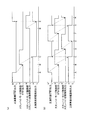
(Standby mode control)
Here, the mechanism of standby mode control by the standby
スタンバイ・モード制御部126は、主演算部125からスタンバイ1状態に入ることを指示する信号(STB1)を受信すると((a)の時刻A)、最終的にスタンバイ1状態に入るか否かの判定を行う。なお、スタンバイ・モード制御部126は、図示されていない入出力部からスタンバイ1状態に入ることを指示する信号(STB1)を受信した場合でも、同様の判定を行う。そして、スタンバイ・モード制御部126がスタンバイ1状態に入ると判定した場合には、電源部124にスタンバイ1状態に入ることを指示する信号(STB1)を送信する((a)の時刻B)。
When the standby
電源部124は、スタンバイ1状態に入ることを指示する信号(STB1)を受け取ると、第3のスイッチング素子149および第1のスイッチング素子147をオフにすることにより、第2の光系用電源部145および主演算部用電源部142への電力供給を切断し((a)の時刻C)、その後、光電気混載集積回路41は、スタンバイ1状態で動作する。この結果、光電気混載集積回路121の消費電力は、大幅に低下する。
When the
スタンバイ1状態では、光配線部123の温度補償部136へ電力を供給する第1の光系用電源部144は、稼動している。この理由を以下に説明する。温度補償部136の動作は温度に関する制御を含むため、電気回路の制御と比較すると大きな時定数を要する。このため、第1の光系用電源部144と、(光配線部123の発光素子131、第1の光分波器134、および、第2の光分波器135へ電力を供給する)第2の光系用電源部145の両方を同時にオフ状態からオン状態へ変更した場合、温度補償部136が安定するまでに時間がかかり、その間、光配線部123の使用を停止しておく必要がある。
In the
これを毎回繰り返すことは、演算時間の損失となるので、主演算部125の演算処理が休止する時間が一定時間以内の場合には、温度補償部136は通電したままの状態で保持しておくほうが望ましい。そこで、第2の光系用電源部145および主演算部用電源部142はオフとなるが、第1の光系用電源部144はオンのまま保持する状態を、スタンバイ1状態としている。
Repeating this every time results in a loss of calculation time. Therefore, if the time during which the calculation processing of the
光電気混載集積回路121がスタンバイ1状態で動作中も、スタンバイ・モード制御部126には、スタンバイ・モード制御部用電源部143から電力が供給され続け、スタンバイ・モード制御を行うことが可能である。例えば、光電気混載集積回路121がスタンバイ1状態で動作中に、図示されていない入出力部を介して外部からの動作状態の問い合わせ信号が入った場合、スタンバイ・モード制御部126は、光電気混載集積回路121がスタンバイ1状態であると連絡する信号を返信する制御を行うことができる。
Even when the opto-electric hybrid
なお、スタンバイ・モード制御部126は、スタンバイ1状態で動作中は、外部からの問い合わせの有無に関わらず、常にスタンバイ1状態であると連絡する信号を発信し続けることも可能であるが、信号を発信し続けることは消費電力の増加を招くので、望ましくは、前述の形態とした方がよい。
While the standby
光電気混載集積回路121がスタンバイ1状態で動作中に、スタンバイ・モード制御部126が、図示されていない入出力部または主演算部125からスタンバイ1状態の解除を指示するスタンバイ1状態解除信号を受信すると((a)の時刻D)、電源部124にスタンバイ1状態解除信号を送信する((a)の時刻E)。
While the opto-electric hybrid
電源部124は、スタンバイ1状態解除信号を受け取ると、シーケンサー146の指示に基づき、第3のスイッチング素子149および第1のスイッチング素子147をオンにすることにより、第2の光系用電源部145および主演算部用電源部142への電力供給を順次再開し((a)の時刻E)、光配線部123を使用した主演算部125の機能が有効となる。そして、主演算部125は、電力供給の再開を受けて、内部メモリ状態の確認等の初期化処理を行い、入出力部からの信号処理の指示が受信可能となる。こうして、光電気混載集積回路121は、通常の状態で動作する。
When the
このように、主演算部の演算処理状態に応じて、通常の稼働状態と、スタンバイ1状態での稼働状態とを適宜切り替えることにより、光電気混載集積回路121は、演算処理の開始時間を遅らせずに、正常な演算処理を行いながら、電力を効率的に消費することができ、結果的に消費電力を大幅に低下することが可能となる。
As described above, the opto-electric hybrid
次に、スタンバイ・モードの制御の仕組みについて説明する。光電気混載集積回路121がスタンバイ1状態に移行後、スタンバイ・モード制御部126が、図示されていない入出力部または主演算部125からスタンバイ1状態の解除を指示するスタンバイ1状態解除信号を、一定の時間受信しなかった場合を考える。
Next, the mechanism of standby mode control will be described. After the opto-electric hybrid
スタンバイ信号生成部130は、スタンバイ1状態に入ることを指示する信号(STB1)を生成後、所定の時間が経過するとスタンバイ・モード(待機状態)に入ることを指示するスタンバイ信号(STB)を生成する。そして、主演算部125は、スタンバイ信号(STB)をスタンバイ・モード制御部126へ送信する。この時、主演算部125(スタンバイ信号生成部130)は、既に停止状態にあるが、停止前に回路内に蓄えられた電荷を利用すること等により、スタンバイ信号(STB)の作成および送信が可能である。
The standby
スタンバイ・モード制御部126は、主演算部125からスタンバイ信号(STB)を受信すると、最終的にスタンバイ・モードに入るか否かの判定を行う。なお、スタンバイ・モード制御部126は、図示されていない入出力部からスタンバイ信号(STB)を受信した場合でも、同様の判定を行う。そして、スタンバイ・モード制御部126がスタンバイ・モードに入ると判定した場合には、電源部124にスタンバイ信号(STB)を送信する。
When the standby
電源部124は、スタンバイ信号(STB)を受け取ると、さらに、第2のスイッチング素子148をオフにすることにより、第1の光系用電源部144への電力供給を切断し、その後、光電気混載集積回路41は、スタンバイ・モードで動作する。この結果、光電気混載集積回路121の消費電力は、スタンバイ1状態に比べ、さらに低下する。
When the
光電気混載集積回路121がスタンバイ・モードで動作中も、スタンバイ・モード制御部126には、スタンバイ・モード制御部用電源部143から電力が供給され続け、スタンバイ・モード制御を行うことが可能である。例えば、光電気混載集積回路121がスタンバイ・モードで動作中に、図示されていない入出力部を介して外部からの動作状態の問い合わせ信号が入った場合、スタンバイ・モード制御部126は、光電気混載集積回路121がスタンバイ・モードであると連絡する信号を返信する制御を行うことができる。
Even when the opto-electric hybrid
なお、スタンバイ・モード制御部126は、スタンバイ・モードで動作中は、外部からの問い合わせの有無に関わらず、常にスタンバイ・モードであると連絡する信号を発信し続けることも可能であるが、信号を発信し続けることは消費電力の増加を招くので、望ましくは、前述の形態とした方がよい。
It should be noted that the standby
光電気混載集積回路121がスタンバイ・モードで動作中に、スタンバイ・モード制御部126は、図示されていない入出力部または主演算部125からスタンバイ・モードの解除を指示するスタンバイ・モード解除信号を受信すると、電源部124にスタンバイ・モード解除信号を送信する。
While the opto-electric hybrid
電源部124は、スタンバイ・モード解除信号を受け取ると、シーケンサー146の指示に基づき、第2のスイッチング素子148、第3のスイッチング素子149、および第1のスイッチング素子147をオンにすることにより、第1の光系用電源部144、第2の光系用電源部145、および、主演算部用電源部142への電力供給を順次再開し、光配線部123を使用した主演算部125の機能が有効となる。そして、主演算部125は、電力供給の再開を受けて、内部メモリ状態の確認等の初期化処理を行い、入出力部からの信号処理の指示が受信可能となる。こうして、光電気混載集積回路121は、通常の状態で動作する。
Upon receiving the standby mode release signal, the
このように、スタンバイ1状態での稼働時間と主演算部の演算処理状態とに応じて、スタンバイ1状態での稼働状態と、スタンバイ・モードでの稼働状態と、通常の稼働状態とを適宜切り替えることにより、光電気混載集積回路121は、正常な演算処理を行いながら、電力を効率的に消費することができ、結果的に消費電力を大幅に低下することが可能となる。
As described above, the operation state in the
本実施の形態では、スタンバイ・モード制御部126は、主演算部125からのスタンバイ1状態に入ることを指示する信号(STB1)を反転論理で受信している。すなわち、スタンバイ信号生成部130が、スタンバイ1状態に入ることを指示する信号(STB1)を反転論理で作成している。このように構成することにより、光電気混載集積回路121がスタンバイ1状態に入り、主演算部125への電力供給が停止した時に、主演算部125から出力される信号が全て0Vとなり、主演算部125からのスタンバイ1状態に入ることを指示する信号(STB1)が、見かけ上反転してしまう事態を防ぐことができる。この理由を、図8の(b)を使用して説明する。
In the present embodiment, the standby
図8の(b)は、スタンバイ・モード制御部126が、主演算部125からのスタンバイ1状態に入ることを指示する信号(STB1)を反転論理で受信しなかった場合のスタンバイ状態1制御のタイミングチャートである。スタンバイ・モード制御部126が、主演算部125からスタンバイ1状態に入ることを指示する信号(STB1)を受信し((b)の時刻A)、スタンバイ1状態に入ると判定した場合には、電源部124にスタンバイ1状態に入ることを指示する信号(STB1)を送信する((b)の時刻B)。電源部124は、スタンバイ1状態に入ることを指示する信号(STB1)を受け取ると、第2の光系用電源部145および主演算部用電源部142への電力供給を切断し((a)の時刻C)、その後、光電気混載集積回路121は、スタンバイ1状態で動作する。
FIG. 8B shows
ところが、電力供給を切断された主演算部125は、スタンバイ1状態に入ることを指示する信号(STB1)を維持することができず、自動的に0V(Lレベル)を出力してしまう((b)の時刻C)。すると、スタンバイ・モード制御部126は、スタンバイ1状態に入ることを指示する信号(STB1)が反転したと受け取り、電源部124にスタンバイ1状態解除信号を出力する((b)の時刻D)。この結果、第2の光系用電源部145および主演算部用電源部142は電力の供給を再開し、電力の供給再開とともに、主演算部125によりスタンバイ1状態に入ることを指示する信号(STB1)が再度出力される(Hレベルになる)((b)の時刻E)。従って、時刻Eの状態は、時刻Aの状態と同じとなり、系は自動的に同じ動作を繰り返す結果((b)の時刻E〜H)、発振状態に陥り、スタンバイ1状態での動作を維持することが不可能となってしまう。
However, the main
この問題を回避するために、スタンバイ・モード制御部126が、主演算部125からのスタンバイ1状態に入ることを指示する信号(STB1)のうち立ち上がり部分(スタンバイ1状態に入る場合)のみを利用し、立ち下がり部分(スタンバイ1状態から復帰する場合)は無視するように、スタンバイ・モード制御部126の演算回路を設計する手法も可能である。しかし、このような演算回路に必要な面積は、反転論理を用いる場合はNOT回路を一個追加するのみで済むことと比較すると、はるかに大きい。
In order to avoid this problem, the standby
このように、反転論理を用いてシステム設計を行うことにより、主演算部125からスタンバイ・モード制御部126へのスタンバイ1状態移行の指示を、簡単な回路設計で、確実に行うことが可能となる。
In this way, by designing the system using inverted logic, it is possible to instruct the
同様に、本実施の形態では、スタンバイ・モード制御部126は、主演算部125からのスタンバイ信号(STB)を反転論理で受信している。すなわち、スタンバイ信号生成部130が、スタンバイ信号(STB)を反転論理で作成している。このように構成することにより、光電気混載集積回路121がスタンバイ・モードに入り、主演算部125への電力供給が停止した時に、主演算部125から出力される信号が全て0Vとなり、主演算部125からのスタンバイ信号(STB)が、見かけ上反転してしまう事態を防ぐことができる。
Similarly, in the present embodiment, the standby
このように、反転論理を用いてシステム設計を行うことにより、主演算部125からスタンバイ・モード制御部126へのスタンバイ・モード移行の指示を、簡単な回路設計で、確実に行うことが可能となる。
In this way, by designing the system using inverted logic, it is possible to instruct the standby mode transition from the main
本実施の形態では、温度補償部136は、温度補償をピエゾ素子の伸縮により行ったが、他の方法で行うことも可能である。例えば、ピエゾ素子の代わりにヒーターを内蔵しておき、ヒーターに印加する電圧を制御することにより、第1の光分波器134および第2の光分波器135の温度を一定に保つことも可能である。あるいは、第1の光分波器134および第2の光分波器135へ印加するバイアス電圧を変化させても、第1の光分波器134および第2の光分波器135の特性が変わるので、この性質を利用して、バイアス電圧の制御を行い、温度による特性変化を、バイアス電圧による特性変化で相殺することも可能である。その他、本発明の要旨を逸脱しない範囲で、種々変形して実施することができる。
In the present embodiment, the
このように、第5の実施の形態にかかる光電気混載集積回路によれば、光配線部の温度補償部と消費電力の大きな発光素子とへの電力供給と、この光配線を用いて信号伝達を行う主演算部への電力供給とを遮断したスタンバイ状態を設けることにより、回路の正常な動作を保証しながら消費電力を大幅に低下させる光電気混載集積回路を提供することが可能である。この結果、携帯機器に代表される、待機状態での低消費電力化が重要となる機器に搭載される光電気混載集積回路において、光配線の利益を享受することが可能となる。 As described above, according to the opto-electric hybrid integrated circuit according to the fifth embodiment, power is supplied to the temperature compensation unit of the optical wiring unit and the light emitting element with large power consumption, and signal transmission is performed using the optical wiring. By providing a standby state in which the power supply to the main arithmetic unit that performs the operation is cut off, it is possible to provide an opto-electric hybrid integrated circuit that greatly reduces power consumption while ensuring normal operation of the circuit. As a result, it is possible to enjoy the benefits of optical wiring in an opto-electric hybrid integrated circuit mounted on a device such as a portable device in which low power consumption is important in a standby state.
さらに、第5の実施の形態にかかる光電気混載集積回路によれば、光配線部の消費電力の大きな発光素子への電力供給と、この光配線を用いて信号伝達を行う主演算部への電力供給とを遮断したスタンバイ1状態を設けることにより、回路の正常な動作を保証しながら、演算処理の開始時間を遅らせずに、消費電力を大幅に低下させる光電気混載集積回路を提供することが可能である。この結果、携帯機器に代表される、待機状態での低消費電力化が重要となる機器に搭載される光電気混載集積回路において、光配線の利益を享受することが可能となる。
Furthermore, according to the opto-electric hybrid integrated circuit according to the fifth embodiment, power is supplied to the light-emitting element having a large power consumption in the optical wiring section, and the signal is transmitted to the main arithmetic section using the optical wiring. Providing an opto-electric hybrid integrated circuit that significantly reduces power consumption without delaying the start time of arithmetic processing while ensuring normal operation of the circuit by providing a
(光電気混載集積回路の製造方法)
第1〜5の実施の形態にかかる光電気混載集積回路の製造方法について説明する。図9は、第1〜5の実施の形態にかかる光電気混載集積回路の断面工程図である。
(Method for manufacturing an opto-electric hybrid integrated circuit)
A method for manufacturing the opto-electric hybrid integrated circuit according to the first to fifth embodiments will be described. FIG. 9 is a sectional process diagram of the opto-electric hybrid integrated circuit according to the first to fifth embodiments.
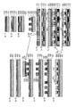
まず、図9の(a−1)に示すように、直径3インチのGaAs基板151に、InおよびSbのイオン注入とアニールによる結晶性回復処理を行い、剥離層152と緩衝層153とを形成する。ついで、図9の(a−2)に示すように、III−V族半導体のエピタキシャル成長により、GaInNAs発光層やInGaAs受光層等を含む、光学素子層154(第5の実施の形態にかかる光電気混載集積回路では、InGaAs受光層や、GaInAsPからなる共振器型の光分波器等を含む、光学素子層154)を形成する。そして、図示されていないが、引出配線部を形成する。引き続き、図9の(a−3)に示すように、スパッタリング法によりSiO2からなる緩衝層155を形成し、最上部を研磨しておく。そして、図9の(a−4)に示すように、ウェハ周辺部を含む、光学素子部として不要な部分をフォトリソグラフィー工程とエッチングにより除去する。
First, as shown in FIG. 9 (a-1), a
一方、図9の(b−1)に示すように、直径12インチのSOI基板161に、水素イオンを注入し、バルク側Siに剥離層162を形成する。ついで、図9の(b−2)に示すように、表面側Si層を加工して、SiO2膜中に埋め込まれたSiからなる光導波路層163(第2〜4の実施の形態にかかる光電気混載集積回路では、ニオブ酸リチウムからなる光変調器と、SiO2膜中に埋め込まれたSiからなる光導波路層163)を形成し、SiO2膜最上部を研磨しておく。ついで、図9の(b−3)に示すように、直接接合を用いて、図9の(a−4)で得られた基板を上下反転して所定の位置に貼り合せる。ついで、図9の(b−4)に示すように、GaAs基板151の裏面より基板剥離光の照射を行い、剥離層152から基板を分離する。ついで、図9の(b−5)に示すように、SOI基板161上の他の所望位置にも図9の(a−4)で得られた基板を順次貼り合せる。そして、図9の(b−6)に示すように、TEOSを用いたプラズマCVD法により、基板全面にSiO2膜164を成膜し、表面を研磨して平坦化する。
On the other hand, as shown in FIG. 9B-1, hydrogen ions are implanted into an
さらに、図9の(c−1)に示すように、直径12インチのSi基板171上に、通常のCMOS工程を用いて、電気回路配線を含むCMOS回路層172を形成する。ついで、図9の(c−2)に示すように、TEOSを用いたプラズマCVD法により、基板全面にSiO2膜173を成膜し、表面を研磨して平坦化する。ついで、図9の(c−3)に示すように、直接接合を用いて、図9の(b−6)で得られた基板を上下反転して所定の位置に貼り合せる。ついで、図9の(c−4)に示すように、先程と異なる波長の光を用いて、SOI基板161の裏面より基板剥離光の照射を行い、剥離層162から基板を分離する。そして、図示されていないが、光学素子層154およびCMOS回路層172を接続する配線層形成工程を行い、最後に、ファイナル・パッシベーション形成、パッド形成等、通常の半導体装置製造工程を経ることにより、光電気混載半導体装置を形成することが可能となる。
Further, as shown in FIG. 9 (c-1), a
そして、発光素子12(第2〜4の実施の形態にかかる光電気混載集積回路では、光変調器37、65、66、67、68、99、100、101、102、第5の実施の形態にかかる光電気混載集積回路では、光分波器134、135)を駆動するNMOSFETが光配線部に備えられているのは、発光素子12(第2〜4の実施の形態にかかる光電気混載集積回路では、光変調器37、65、66、67、68、99、100、101、102、第5の実施の形態にかかる光電気混載集積回路では、光分波器134、135)の消費電力が大きいため、駆動力の大きなFETが必要とされることから、このFETと演算部のFETを別の基板に異なる工程条件で製作したほうが好都合なためである。製造工程を簡略化し、FETの設計改良により、発光素子12(第2〜4の実施の形態にかかる光電気混載集積回路では、光変調器37、65、66、67、68、99、100、101、102、第5の実施の形態にかかる光電気混載集積回路では、光分波器134、135)を駆動するNMOSFETを主演算部5、45、125に取り込むことも可能であり、この場合には、低コスト化を図ることができる利点がある。
The light emitting element 12 (in the opto-electric hybrid integrated circuit according to the second to fourth embodiments, the
このように、第1〜5の実施の形態にかかる光電気混載集積回路の製造方法によれば、消費電力の少ない光電気混載集積回路を製造する方法を提供することが可能である。 Thus, according to the manufacturing method of the opto-electric hybrid integrated circuit according to the first to fifth embodiments, it is possible to provide a method of manufacturing the opto-electric hybrid integrated circuit with low power consumption.
(変形例)
なお、本発明は上述した各実施形態に限定されるものではない。図10は、光電気混載集積回路の変形例を示す図である。第1および第2の実施形態を説明する図では、一組の光配線のみ記載されているが、実際の光電気混載集積回路では複数の光配線が使用されるので、図10の(a)または図10の(b)のように、複数の素子が並列に接続されることが一般的である。また、一つの出力を二ヶ所以上の入力に接続することも可能であり、光導波路13を分岐して、異なる受光素子14に、それぞれ接続すればよい。
(Modification)
The present invention is not limited to the above-described embodiments. FIG. 10 is a diagram showing a modification of the opto-electric hybrid integrated circuit. In the figures for explaining the first and second embodiments, only one set of optical wirings is shown, but in an actual opto-electric hybrid integrated circuit, a plurality of optical wirings are used. Or, as shown in FIG. 10B, a plurality of elements are generally connected in parallel. Further, one output can be connected to two or more inputs, and the
また、発光素子12としてGaInNAsを用いたが、GaInAsP等の他の材料を用いることも可能である。さらに、受光素子14としてInGaAsを用いたが、GeやGaSb等の他の材料を用いることも可能である。そして、光導波路13および光導波路181としてSiを用いたが、SiNやSiON等の他の材料を用いることも可能である。光変調器38に関しても、ニオブ酸リチウムを用いた位相変調型(干渉型)のものに限らず、InGaAsPを用いた強度変調型(吸収型)のものを使用することも可能である。その他、本発明の要旨を逸脱しない範囲で、種々変形して実施することができる。
Further, although GaInNAs is used as the
本発明は、制御部と演算部に分離可能な集積回路に有用である。 The present invention is useful for an integrated circuit that can be separated into a control unit and a calculation unit.
1、31、41、91、121 光電気混載集積回路
2、32、42、122 演算部
3、33、43、92、123 光配線部
4、34、44、124 電源部(電源制御部)
5、45、125 主演算部
6、35、46、126 スタンバイ・モード制御部
7、47、127 第1の演算ブロック
8、48、128 第2の演算ブロック
9、49、129 第3の演算ブロック
10、57、130 スタンバイ信号生成部
11、22、23 発光素子駆動部
12、131 発光素子
13 光導波路
14 受光素子
15、81、142 主演算部用電源部
16、82、143 スタンバイ・モード制御部用電源部
17、83 光源用電源部
18、85、146 (ブートアップ)シーケンサー
19、86、147 第1のスイッチング素子
20、39、87、148 第2のスイッチング素子
36 光変調器変調部
37 光変調器
38、84 光系用電源部
50 第4の演算ブロック
51 第5の演算ブロック
52 第1のスイッチ
53 第2のスイッチ
54 第3のスイッチ
55 第4のスイッチ
56 第5のスイッチ
58 状態信号生成部
59、93 第1の発光素子
60、94 第2の発光素子
61、95 第1の光変調器変調部
62、96 第2の光変調器変調部
63、97 第3の光変調器変調部
64、98 第4の光変調器変調部
65、99 第1の光変調器
66、100 第2の光変調器
67、101 第3の光変調器
68、102 第4の光変調器
69、103、137 第1の光導波路
70、104、138 第2の光導波路
71、105、139 第3の光導波路
72、106 第4の光導波路
73、107、140 第1の受光素子
74、108、141 第2の受光素子
75、109 第6のスイッチ
76、110 第7のスイッチ
77、111 第8のスイッチ
78、112 第9のスイッチ
79、113 第10のスイッチ
80、114 第11のスイッチ
88、149 第3のスイッチング素子
132 第1の印加電圧変更部
133 第2の印加電圧変更部
134 第1の光分波器
135 第2の光分波器
136 温度補償部
144 第1の光系用電源部
145 第2の光系用電源部
151 GaAs基板
152 剥離層
153 緩衝層
154 光学素子層
155 緩衝層
161 SOI基板
162 剥離層
163 光導波路層
171 Si基板
172 CMOS回路層
173 SiO2膜
181 光導波路
1, 31, 41, 91, 121 Opto-electric hybrid
5, 45, 125 Main calculation unit 6, 35, 46, 126 Standby mode control unit 7, 47, 127 First calculation block 8, 48, 128 Second calculation block 9, 49, 129 Third calculation block 10, 57, 130 Standby signal generation unit 11, 22, 23 Light emitting element driving unit 12, 131 Light emitting element 13 Optical waveguide 14 Light receiving element 15, 81, 142 Main arithmetic unit power source unit 16, 82, 143 Standby mode control unit Power supply unit 17, 83 light source power supply unit 18, 85, 146 (boot-up) sequencer 19, 86, 147 first switching element 20, 39, 87, 148 second switching element 36 optical modulator modulation unit 37 light Modulators 38 and 84 Power supply unit for optical system 50 Fourth arithmetic block 51 Fifth arithmetic block 52 First switch 3 2nd switch 54 3rd switch 55 4th switch 56 5th switch 58 Status signal generation part 59, 93 1st light emitting element 60, 94 2nd light emitting element 61, 95 1st optical modulator Modulators 62 and 96 Second optical modulator modulators 63 and 97 Third optical modulator modulators 64 and 98 Fourth optical modulator modulators 65 and 99 First optical modulators 66 and 100 Second Optical modulator 67, 101 Third optical modulator 68, 102 Fourth optical modulator 69, 103, 137 First optical waveguide 70, 104, 138 Second optical waveguide 71, 105, 139 Third optical waveguide Waveguide 72, 106 Fourth optical waveguide 73, 107, 140 First light receiving element 74, 108, 141 Second light receiving element 75, 109 Sixth switch 76, 110 Seventh switch 77, 111 Eighth switch 7 8, 112 Ninth switch 79, 113 Tenth switch 80, 114 Eleventh switch 88, 149 Third switching element 132 First applied voltage changing unit 133 Second applied voltage changing unit 134 First light Demultiplexer 135 Second optical demultiplexer 136 Temperature compensation unit 144 First optical system power supply unit 145 Second optical system power supply unit 151 GaAs substrate 152 Release layer 153 Buffer layer 154 Optical element layer 155 Buffer layer 161 SOI substrate 162 Release layer 163 Optical waveguide layer 171 Si substrate 172 CMOS circuit layer 173 SiO2 film 181 Optical waveguide
Claims (14)
前記演算手段の一部で演算された結果である電気信号を光信号に変換し、前記演算手段の他の部分へ光信号で伝達後、再び電気信号に変換する光信号伝達手段と、
前記演算手段と前記光信号伝達手段とに電力を供給する電源手段と、
前記電源手段による前記光信号伝達手段への電力の供給と、前記電源手段による前記演算手段への電力の供給とを制御する電源制御手段と、を備え、
前記電源制御手段は、前記演算手段の待機状態と稼働状態とを切り換える待機状態信号に応じて、光信号伝達手段への電力の供給と演算手段への電力の供給とを遮断し、
前記演算手段は、前記待機状態信号を生成する待機状態信号生成手段を含み、
前記待機状態信号生成手段は、前記演算手段の各部から演算処理を休止している状態であることを示す信号を反転論理で受け取ることにより、前記待機状態信号を反転論理で生成すること、
を特徴とする光電気混載集積回路。 A calculation means for performing a calculation;
An optical signal transmission means for converting an electric signal, which is a result calculated by a part of the arithmetic means, into an optical signal, transmitting the optical signal to the other part of the arithmetic means, and then converting the electric signal again;
Power supply means for supplying power to the arithmetic means and the optical signal transmission means;
Power supply control means for controlling power supply to the optical signal transmission means by the power supply means and power supply to the computing means by the power supply means,
The power supply control means shuts off the supply of power to the optical signal transmission means and the supply of power to the calculation means in response to a standby state signal for switching between the standby state and the operation state of the calculation means,
The computing means includes standby state signal generating means for generating the standby state signal,
The standby state signal generation means generates the standby state signal with inverted logic by receiving a signal indicating that the arithmetic processing is suspended from each part of the arithmetic means with inverted logic.
An opto-electric hybrid integrated circuit.
を特徴とする請求項1に記載の光電気混載集積回路。 The power supply means includes at least one first switch means for connecting or blocking power supply to the computing means and power supply to the optical signal transmission means;
The opto-electric hybrid integrated circuit according to claim 1 .
を特徴とする請求項2に記載の光電気混載集積回路。 The first switch means is disposed on an input side of a part of the power supply means that supplies power to the arithmetic means and an input side of a part of the power supply means that supplies power to the optical signal transmission means. That
The opto-electric hybrid integrated circuit according to claim 2 .
前記光信号伝達手段は、さらに、前記光信号伝達手段の各部への電力の供給を、接続または遮断する少なくとも一つの第3のスイッチ手段を備え、
前記電源制御手段は、前記第2のスイッチ手段と前記第3のスイッチ手段とを制御すること、
を特徴とする請求項1〜3のいずれか一項に記載の光電気混載集積回路。 The calculation means further includes at least one second switch means for connecting or cutting off power supply to each part of the calculation means,
The optical signal transmission means further includes at least one third switch means for connecting or blocking power supply to each part of the optical signal transmission means,
The power control means controls the second switch means and the third switch means;
The opto-electric hybrid integrated circuit according to any one of claims 1 to 3 .
を特徴とする請求項1〜4のいずれか一項に記載の光電気混載集積回路。 The power supply means further supplies power to the power supply control means;
The opto-electric hybrid integrated circuit according to any one of claims 1 to 4 .
を特徴とする請求項1〜5のいずれか一項に記載の光電気混載集積回路。 The optical signal transmission means comprises at least one set of light emitting means, light receiving means and optical waveguide means;
An opto-electric hybrid integrated circuit according to any one of claims 1 to 5 .
を特徴とする請求項1〜6のいずれか一項に記載の光電気混載集積回路。 The optical signal transmission means comprises at least one light emitting means and at least one set of light modulating means, light receiving means and optical waveguide means;
The opto-electric hybrid integrated circuit according to any one of claims 1 to 6 .
前記演算手段の一部で演算された結果である電気信号を光信号に変換し、前記演算手段の他の部分へ光信号で伝達後、再び電気信号に変換する光信号伝達手段と、
前記光信号伝達手段の動作状態を安定させる安定化手段と、
前記演算手段、前記光信号伝達手段、および、前記安定化手段に電力を供給する電源手段と、
前記電源手段による前記光信号伝達手段への電力の供給、前記電源手段による前記安定化手段への電力の供給、および、前記電源手段による前記演算手段への電力の供給を制御する電源制御手段と、を備え、
前記電源制御手段は、
前記演算手段の待機状態と稼働状態とを切り換える第1の待機状態信号に応じて、前記光信号伝達手段への電力の供給と、前記演算手段への電力の供給とを制御し、
前記演算手段の待機状態と稼働状態とを切り換える第2の待機状態信号に応じて、前記安定化手段への電力の供給を遮断し、
前記演算手段は、前記第1の待機状態信号と前記第2の待機状態信号とを生成する待機状態信号生成手段を含み、
前記待機状態信号生成手段は、前記演算手段の各部から演算処理を休止している状態であることを示す信号を反転論理で受け取ることにより、前記第1の待機状態信号と前記第2の待機状態信号とを反転論理で生成すること、
を特徴とする光電気混載集積回路。 A calculation means for performing a calculation;
An optical signal transmission means for converting an electric signal, which is a result calculated by a part of the arithmetic means, into an optical signal, transmitting the optical signal to the other part of the arithmetic means, and then converting the electric signal again;
Stabilizing means for stabilizing the operating state of the optical signal transmitting means;
Power supply means for supplying power to the arithmetic means, the optical signal transmission means, and the stabilization means;
Power supply means for controlling power supply to the optical signal transmission means by the power supply means, power supply to the stabilization means by the power supply means, and power supply to the computing means by the power supply means; With
The power control means includes
In response to a first standby state signal that switches between a standby state and an operating state of the arithmetic means, controlling the supply of power to the optical signal transmission means and the supply of power to the arithmetic means,
In response to a second standby state signal for switching between the standby state and the operating state of the computing means, the supply of power to the stabilizing means is shut off ,
The computing means includes standby state signal generating means for generating the first standby state signal and the second standby state signal,
The standby state signal generating means receives the first standby state signal and the second standby state from each part of the arithmetic means by receiving a signal indicating that the arithmetic processing is suspended in inverted logic. Generating signals with inverted logic,
An opto-electric hybrid integrated circuit.
を特徴とする請求項8に記載の光電気混載集積回路。 The power supply means includes at least one first switch means for connecting or blocking power supply to the computing means, power supply to the stabilization means, and power supply to the optical signal transmission means. Providing
The opto-electric hybrid integrated circuit according to claim 8 .
を特徴とする請求項9に記載の光電気混載集積回路。 The first switch means includes an input side of a portion of the power supply means that supplies power to the arithmetic means, an input side of a portion of the power supply means that supplies power to the stabilization means, and the power supply Arranged on the input side of the portion for supplying power to the optical signal transmission means in the means,
The opto-electric hybrid integrated circuit according to claim 9 .
前記光信号伝達手段は、さらに、前記光信号伝達手段の各部への電力の供給を接続または遮断する少なくとも一つの第3のスイッチ手段を備え、
前記電源制御手段は、前記第2のスイッチ手段と前記第3のスイッチ手段とを制御すること、
を特徴とする請求項8〜10のいずれか一項に記載の光電気混載集積回路。 The calculation means further comprises at least one second switch means for connecting or cutting off the supply of power to each part of the calculation means,
The optical signal transmission means further includes at least one third switch means for connecting or blocking power supply to each part of the optical signal transmission means,
The power control means controls the second switch means and the third switch means;
The opto-electric hybrid integrated circuit according to any one of claims 8 to 10 .
を特徴とする請求項8〜11のいずれか一項に記載の光電気混載集積回路。 The power supply means further supplies power to the power supply control means;
The opto-electric hybrid integrated circuit according to any one of claims 8 to 11 .
を特徴とする請求項8〜12のいずれか一項に記載の光電気混載集積回路。 The optical signal transmission means comprises at least one set of light emitting means, light receiving means and optical waveguide means;
The opto-electric hybrid integrated circuit according to any one of claims 8 to 12 .
を特徴とする請求項8〜13のいずれか一項に記載の光電気混載集積回路。 The optical signal transmission means comprises at least one light emitting means and at least one set of light modulating means, light receiving means and optical waveguide means;
The opto-electric hybrid integrated circuit according to any one of claims 8 to 13 .
Priority Applications (2)
| Application Number | Priority Date | Filing Date | Title |
|---|---|---|---|
| JP2007077388A JP5111913B2 (en) | 2007-03-23 | 2007-03-23 | Opto-electric hybrid integrated circuit |
| US12/033,330 US8086107B2 (en) | 2007-03-23 | 2008-02-19 | Optical-electrical hybrid integrated circuit |
Applications Claiming Priority (1)
| Application Number | Priority Date | Filing Date | Title |
|---|---|---|---|
| JP2007077388A JP5111913B2 (en) | 2007-03-23 | 2007-03-23 | Opto-electric hybrid integrated circuit |
Publications (2)
| Publication Number | Publication Date |
|---|---|
| JP2008233821A JP2008233821A (en) | 2008-10-02 |
| JP5111913B2 true JP5111913B2 (en) | 2013-01-09 |
Family
ID=39906635
Family Applications (1)
| Application Number | Title | Priority Date | Filing Date |
|---|---|---|---|
| JP2007077388A Expired - Fee Related JP5111913B2 (en) | 2007-03-23 | 2007-03-23 | Opto-electric hybrid integrated circuit |
Country Status (2)
| Country | Link |
|---|---|
| US (1) | US8086107B2 (en) |
| JP (1) | JP5111913B2 (en) |
Family Cites Families (10)
| Publication number | Priority date | Publication date | Assignee | Title |
|---|---|---|---|---|
| US5429070A (en) * | 1989-06-13 | 1995-07-04 | Plasma & Materials Technologies, Inc. | High density plasma deposition and etching apparatus |
| US5122251A (en) * | 1989-06-13 | 1992-06-16 | Plasma & Materials Technologies, Inc. | High density plasma deposition and etching apparatus |
| US4990229A (en) * | 1989-06-13 | 1991-02-05 | Plasma & Materials Technologies, Inc. | High density plasma deposition and etching apparatus |
| US5091049A (en) * | 1989-06-13 | 1992-02-25 | Plasma & Materials Technologies, Inc. | High density plasma deposition and etching apparatus |
| US5421891A (en) * | 1989-06-13 | 1995-06-06 | Plasma & Materials Technologies, Inc. | High density plasma deposition and etching apparatus |
| US5653811A (en) * | 1995-07-19 | 1997-08-05 | Chan; Chung | System for the plasma treatment of large area substrates |
| JP3719800B2 (en) * | 1996-12-26 | 2005-11-24 | 沖電気工業株式会社 | Optical communication apparatus and optical communication system |
| JP2006091241A (en) | 2004-09-22 | 2006-04-06 | Hitachi Cable Ltd | Optoelectronic composite wiring component and electronic equipment using the same |
| JP2006023777A (en) | 2005-09-15 | 2006-01-26 | Seiko Epson Corp | Optical module, optical communication apparatus, photoelectric consolidated integrated circuit, circuit board and electronic apparatus |
| KR20080035173A (en) * | 2006-10-18 | 2008-04-23 | 삼성전자주식회사 | Air conditioner and control method thereof |
-
2007
- 2007-03-23 JP JP2007077388A patent/JP5111913B2/en not_active Expired - Fee Related
-
2008
- 2008-02-19 US US12/033,330 patent/US8086107B2/en active Active
Also Published As
| Publication number | Publication date |
|---|---|
| US20080292319A1 (en) | 2008-11-27 |
| JP2008233821A (en) | 2008-10-02 |
| US8086107B2 (en) | 2011-12-27 |
Similar Documents
| Publication | Publication Date | Title |
|---|---|---|
| Ahn et al. | Devices and architectures for photonic chip-scale integration | |
| US20190027899A1 (en) | Rapidly Tunable Silicon Modulated Laser | |
| JP5984958B2 (en) | Electronic / photonic integrated circuit architecture and manufacturing method thereof | |
| US20130322813A1 (en) | Low loss directional coupling between highly dissimilar optical waveguides for high refractive index integrated photonic circuits | |
| JP2007178550A (en) | Optical functional element, its driving method and its manufacturing method | |
| CN101866066A (en) | Phase change material-aid micro ring-based optical waveguide switch | |
| WO2007023858A1 (en) | Automatic regulation system of fsk modulator | |
| JP2018527767A5 (en) | ||
| CN109361149B (en) | Silicon-based tunable laser | |
| CN114616513A (en) | Optical module | |
| JP2009128718A (en) | Optical switch | |
| EP1200859A1 (en) | Optical planar waveguide device and method of fabrication | |
| US20200350993A1 (en) | Method and system for a distributed optical transmitter with local domain splitting | |
| JP4421951B2 (en) | Optical transmission module | |
| JP5111913B2 (en) | Opto-electric hybrid integrated circuit | |
| EP3961278A1 (en) | Power-efficient integrated photonic switch | |
| JP6545020B2 (en) | Modulated light source | |
| JP2007256716A (en) | Optical transmitter | |
| Wang et al. | On-chip optical interconnects using ingan light-emitting diodes integrated with si-cmos | |
| JP2004163675A (en) | Organic waveguide type optical modulator with monitor, optical modulation apparatus and optical integrated circuit | |
| JP2010032856A (en) | Optical signal modulation method and optical signal modulator | |
| Li et al. | A CMOS wafer-scale, monolithically integrated WDM platform for TB/s optical interconnects | |
| JP7187623B1 (en) | High-bandwidth photonic integrated circuits with etalon compensation | |
| AlTaha et al. | Silicon-photonic devices: Electronic control and stabilization | |
| JP7117435B2 (en) | Power feeding communication device and power receiving communication device |
Legal Events
| Date | Code | Title | Description |
|---|---|---|---|
| A621 | Written request for application examination |
Free format text: JAPANESE INTERMEDIATE CODE: A621 Effective date: 20090326 |
|
| A131 | Notification of reasons for refusal |
Free format text: JAPANESE INTERMEDIATE CODE: A131 Effective date: 20120626 |
|
| A521 | Written amendment |
Free format text: JAPANESE INTERMEDIATE CODE: A523 Effective date: 20120824 |
|
| TRDD | Decision of grant or rejection written | ||
| A01 | Written decision to grant a patent or to grant a registration (utility model) |
Free format text: JAPANESE INTERMEDIATE CODE: A01 Effective date: 20120911 |
|
| A01 | Written decision to grant a patent or to grant a registration (utility model) |
Free format text: JAPANESE INTERMEDIATE CODE: A01 |
|
| A61 | First payment of annual fees (during grant procedure) |
Free format text: JAPANESE INTERMEDIATE CODE: A61 Effective date: 20121010 |
|
| FPAY | Renewal fee payment (event date is renewal date of database) |
Free format text: PAYMENT UNTIL: 20151019 Year of fee payment: 3 |
|
| FPAY | Renewal fee payment (event date is renewal date of database) |
Free format text: PAYMENT UNTIL: 20151019 Year of fee payment: 3 |
|
| LAPS | Cancellation because of no payment of annual fees |