JP5111236B2 - Data transfer system - Google Patents
Data transfer system Download PDFInfo
- Publication number
- JP5111236B2 JP5111236B2 JP2008134509A JP2008134509A JP5111236B2 JP 5111236 B2 JP5111236 B2 JP 5111236B2 JP 2008134509 A JP2008134509 A JP 2008134509A JP 2008134509 A JP2008134509 A JP 2008134509A JP 5111236 B2 JP5111236 B2 JP 5111236B2
- Authority
- JP
- Japan
- Prior art keywords
- switch
- route
- data transfer
- pci express
- transfer system
- Prior art date
- Legal status (The legal status is an assumption and is not a legal conclusion. Google has not performed a legal analysis and makes no representation as to the accuracy of the status listed.)
- Expired - Fee Related
Links
Images


Landscapes
- Bus Control (AREA)
Description
本発明は、データ転送システムに係り、特に、用途に最適な経路を設定してデータ転送を制御するデータ転送システムに関する。 The present invention relates to a data transfer system, and more particularly, to a data transfer system that controls data transfer by setting a route optimal for a use.
近年、情報処理装置に採用されるI/Oインターフェースは、性能要件の向上に伴い、PCI(TM)、PCI−X(TM)等のパラレルバスから、PCI Express (TM)等の高速シリアルインターフェースに置き換わりつつある。 In recent years, I / O interfaces adopted in information processing apparatuses have been changed from parallel buses such as PCI (TM) and PCI-X (TM) to high-speed serial interfaces such as PCI Express (TM) as performance requirements have improved. It is being replaced.
PCI Express は、従来のパラレルバスとは異なり、デバイス間を1対1で接続することができるため、ホストが備えるポート数以上のスロット数を実装したい場合等にしばしばPCI Express スイッチが使用される。 Unlike conventional parallel buses, PCI Express can connect devices in a one-to-one relationship, so PCI Express switches are often used when it is desired to install more slots than the number of ports provided in the host.
PCI Express スイッチは、スロット数の拡張だけではなく、複数のホストによるI/O資源の共有、I/Oの冗長構成、I/Oの仮想化等の幅広い応用が可能である。なお、この種のPCI Express スイッチの応用に関する各種の技術が、例えば、非特許文献1等に記載されて知られている。
前述したように、PCI Express スイッチは、様々な応用が期待されるが、一方で、PCI Express カードやそれに関連するソフトウエアが、PCI Express スイッチを経由する使用方法に対応していない場合や、PCI Express スイッチを経由する際に増加するレイテンシが性能上無視できない場合等、PCI Express スイッチを経由したくない場合がある。 As described above, the PCI Express switch is expected to have various applications. On the other hand, if the PCI Express card and related software do not support the usage via the PCI Express switch, There are cases where you do not want to go through the PCI Express switch, such as when the increased latency when going through the Express switch cannot be ignored in terms of performance.
本発明の目的は、前述したような点に鑑み、PCI Express スイッチを含むシステムにおいて、用途に最適な経路を設定することを可能にしたデータ転送システムを提供することにある。 In view of the above-described points, an object of the present invention is to provide a data transfer system capable of setting an optimum route for use in a system including a PCI Express switch.
本発明によれば前記目的は、PCI Express リンクを用いたデータ転送システムであって、 ルートコンプレックスと、PCI Express デバイスに接続されたアドインカードのそれぞれが接続される少なくとも1つのスロットと、パケットスイッチと、経路を選択する経路選択手段とを備え、前記経路選択手段は、前記ルートコンプレックスと前記スロットとの間のデータ転送用の経路について、前記パケットスイッチを介する経路と、前記パケットスイッチを経由しない経路とを、前記アドインカードの性能に応じて選択することにより達成される。 According to the present invention, the object is a data transfer system using a PCI Express link, in which a route complex, at least one slot to which each add-in card connected to a PCI Express device is connected , a packet switch, Route selection means for selecting a route, wherein the route selection means includes a route for passing data between the route complex and the slot, a route through the packet switch, and a route not through the packet switch. According to the performance of the add-in card .
本発明によれば、ユーザは、用途に応じた最適なデータ転送経路を選択して使用することが可能となる。 According to the present invention, the user can select and use an optimal data transfer path according to the application.
以下、本発明によるデータ転送システムの実施形態を図面により詳細に説明する。 Embodiments of a data transfer system according to the present invention will be described below in detail with reference to the drawings.
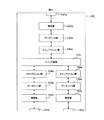
図1は本発明の第1の実施形態によるデータ転送システムの構成例を示すブロック図である。図1に示す本発明の第1の実施形態によるデータ転送システムは、3ポートのPCI Express スイッチ(以下、単に、スイッチという)を、メインボード上に搭載して構成した例である。なお、PCI Express スイッチは、一般に、マルチプレクサ等のスイッチとの区別のために、パケットスイッチと呼ばれている。 FIG. 1 is a block diagram showing a configuration example of a data transfer system according to the first embodiment of the present invention. The data transfer system according to the first embodiment of the present invention shown in FIG. 1 is an example in which a 3-port PCI Express switch (hereinafter simply referred to as a switch) is mounted on a main board. The PCI Express switch is generally called a packet switch in order to distinguish it from a switch such as a multiplexer.
そして、図1(a)に示す構成例は、メインボード100におけるルートコンプレックス110からスロット140a及びスロット140bまでの経路が、スイッチ130を経由するように設定が施された構成例を示し、図1(b)に示す構成例は、メインボード100におけるルートコンプレックス110からスロット140a及びスロット140bまでの経路が、スイッチ130を迂回するように設定が施された構成例を示している。また、図1(a)、図1(b)に示す例は、スイッチ130を経由する経路を作成するか否かを制御するために、ルートコンプレックス110とスロット140a及びスロット140bとの間に、マルチプレクサ120a、スイッチ130、マルチプレクサ120b、120cが設けられて図示のように構成されている。
The configuration example shown in FIG. 1A shows a configuration example in which the route from the
前述において、ルートコンプレックス110は、PCI規格における最上位の親となるコントローラであり、一般には、図示しないホストコンピュータ等の情報処理装置に接続される。また、スロット140a、140bには、図1(a)の場合、アドインカード200a、200bが経路150j、150iを介して接続され、図1(b)の場合、アドインカード200c、200dが経路150j、150iを介して接続されている。これらのアドインカードには、ネットワーク、記憶装置、I/O等を含む図示しないPCI Express デバイスが接続され、また、これらのアドインカードは、接続されるPCI Express デバイスに対するコントローラの機能を有する。なお、ルートコンプレックス及びアドインカードの機能等については、後述する本発明の他の実施形態においても前述と同様である。
In the above description, the
図1(a)に示す例において、ルートコンプレックス110のリンクは、16レーン幅の1ポートに設定され、経路150aを経てマルチプレクサ120aに接続される。また、マルチプレクサ120aは、ルートコンプレックス110とスイッチ130との接続を16レーン幅で経路150a、150bを経てリンクするように設定する。マルチプレクサ120bは、スイッチ130とアドインカード200aとの接続をスロット140aを介して、経路150f、150h、150jを経て16レーン幅でリンクするように設定する。マルチプレクサ120cは、スイッチ130とアドインカード200bとの接続をスロット140bを介して、経路150e、150g、150iを経て16レーン幅でリンクするよう設定する。各マルチプレクサの設定は、共通のセレクト信号160を用いて行われる。このセレクト信号160は、図示しないボード管理用のコントローラを介して、ホストコンピュータから指示されるものであっても、また、図示しないサービスプロセッサを用いて利用者等により指示されるものであってもよく、後述する本発明の第2及び第4の実施形態の場合も同様である。
In the example shown in FIG. 1A, the link of the
図1(b)に示す例において、ルートコンプレックス110のリンクは、8レーン幅の2ポートに分割され、経路150k、150lを経てマルチプレクサ120aに接続される。また、マルチプレクサ120aは、ルートコンプレックス110とスロット140aとを、マルチプレクサ120a及びマルチプレクサ120bを介して8レーン幅で経路150l、150d、150hを経てスイッチ130を介することなく接続するように直接リンクさせ、ルートコンプレックス110とスロット140bとを、マルチプレクサ120a及びマルチプレクサ120cを介して8レーン幅で経路150k、150c、150gを経てスイッチ130を介することなく接続するように直接リンクさせている。
In the example shown in FIG. 1B, the link of the
前述で説明した図1(a)、図1(b)に示す本発明の第1の実施形態によれば、ルートコンプレックス110に接続された図示しないホストコンピュータは、用途に応じて、スイッチ130を介したデータ転送経路を経由して、アドインカードに接続されたPCI Express デバイスを使用する経路と、スイッチ130を介することのないデータ転送経路を経由して、アドインカードに接続されたPCI Express デバイスを使用する経路とを使い分けることができる。
According to the first embodiment of the present invention shown in FIG. 1A and FIG. 1B described above, a host computer (not shown) connected to the
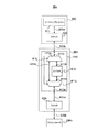
図2は図1に示すPCI Express スイッチ130の内部構成を示すブロック図である。
FIG. 2 is a block diagram showing an internal configuration of the
図2に示すように、PCI Express スイッチ130は、図1(a)、図1(b)に示しているルートコンプレックス110とリンクするポート131aと、スロット140a、140bとリンクし、アドインカードに接続されるPCI Express デバイスとリンクするポート131b、131cと、これらのポート131a〜131c相互間の接続を制御するスイッチ論理135とを備えている。また、図2に示すスイッチ130は、前述のポート131a〜131cのそれぞれと、スイッチ論理135との間には、物理層132a〜132c、データリンク層133a〜133c、トランザクション層134a〜134cが設けられている。
As shown in FIG. 2, the
前述において、物理層132a〜132cは、転送データのシリアル化・非シリアル化、8ビットデータを10ビットデータの時間幅で転送するようにPCI規格による10b/8b変換等の処理を行う。データリンク層133a〜133cは、主にリンクの管理とエラー検出・訂正との処理を行う。トランザクション層134a〜134cは、トランザクションレイヤパケット(TLP)の分解・生成の処理を行うと共に、相手側のデバイスとのパケット交換のフローコントロールの処理を担う。スイッチ論理135は、各ポートのトランザクション層間のパケットをルーティングする。そして、スイッチ論理135は、ポート131aとポート131bとの間、ポート131aとポート131cとの間のデータ転送に限らず、ポート131bとポート131cとの間のいわゆるpeer-to-peer転送も行うことが可能である。
In the above description, the physical layers 132a to 132c perform processing such as serialization / deserialization of transfer data and 10b / 8b conversion according to the PCI standard so that 8-bit data is transferred with a time width of 10-bit data. The
前述したように構成されるスイッチ130は、一般に、このスイッチによるパケットのルーティングを行う際に、前述した各階層の処理に起因するレイテンシが増加することが知られている。
It is known that the
図3はスイッチ130のソフトウェアから見たトポロジを示す図である。
FIG. 3 is a diagram showing the topology viewed from the software of the
PCI Express は、ソフトウエアの互換性を維持するため、PCI互換のコンフィグレーションメカニズムが採用される。各ポート131a〜131cは、仮想PCIバス137a〜137cを介して仮想PCI to PCIブリッジ136a〜136cに接続される。仮想PCI to PCIブリッジ相互間の通信は、仮想PCIバス138上で行われる。コンフィグレーションソフトウェアは、各仮想PCIバス137a〜137c、138のそれぞれが異なるバス番号となるように、各仮想PCI to PCIブリッジのコンフィグレーション空間レジスタを設定する。
PCI Express employs a PCI-compatible configuration mechanism to maintain software compatibility. Each
図1(a)に示して説明した構成例では、ルートコンプレックス110とスイッチ130との間、及び、2つのアドインカード200a、200bとスイッチ130との間が、全て16レーン幅でリンクしている。ルートコンプレックスと両アドインカードとの間の合計スループットは、ルートコンプレックス110とスイッチ130との間の16レーン幅に制限されるものの、アドインカード200aとルートコンプレックス110との間、アドインカード200bとルートコンプレックス110との間の通信が重ならない場合、それぞれ16レーン幅のスループットを享受することができる。また、図1(a)に示して説明した構成例の場合の最大スループットは、図1(b)に示して説明した構成例の場合における8レーン幅と比べて、アドインカード同士がpeer-to-peer転送をサポートする場合のアドインカード200aとアドインカード200bとがスイッチ130を介して通信を行う16レーン幅となる。
In the configuration example illustrated in FIG. 1A, the
図1(b)に示して説明した構成例では、ルートコンプレックス110とアドインカード200c、200dが直接リンクするため、図1(a)に示した構成例の場合のように、スイッチ130を経由する際のレイテンシを増加させることがない。このため、アドインカードの性能がレイテンシに左右されやすい場合には、図1(a)に示す構成例のものを使用する場合に比較して、図1(b)に示す構成例のものを使用する方が性能面で有利となる。また、アドインカードを扱うソフトウェアがスイッチ130による仮想PCI-to-PCIブリッジを介した使用をサポートしていないような場合には、システムの構成を図1(b)に示す構成例とすることによりアドインカードを使用することが可能となる。
In the configuration example shown and described in FIG. 1B, the
前述した本発明の第1の実施形態によるデータ転送システムは、3ポートのPCI Express スイッチを用いるとしたが、この実施形態は、2ポートのPCI Express スイッチを用いても、あるいは、3ポート以上のPCI Express スイッチを用いてもよい。 The above-described data transfer system according to the first embodiment of the present invention uses a 3-port PCI Express switch. However, this embodiment uses a 2-port PCI Express switch, or a 3-port or more PCI Express switch. PCI Express switch may be used.
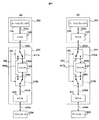
図4は本発明の第2の実施形態によるデータ転送システムの構成例を示すブロック図である。図4に示す本発明の第2の実施形態は、I/O仮想化機構を含む2ポートのスイッチをライザーカードに搭載した場合の構成例である。 FIG. 4 is a block diagram showing a configuration example of a data transfer system according to the second embodiment of the present invention. The second embodiment of the present invention shown in FIG. 4 is a configuration example when a 2-port switch including an I / O virtualization mechanism is mounted on a riser card.
一般に、仮想化環境での性能を向上させる手段として、I/O仮想化機構が知られている。そして、I/O仮想化機構に対応していない既存のハードウエアを最小限の変更で対応させる方法として、メインボード上に搭載するライザーカードの追加あるいは変更という形態がある。本発明の第2の実施形態は、この場合の構成例である。 In general, an I / O virtualization mechanism is known as means for improving performance in a virtual environment. As a method of making existing hardware that does not support the I / O virtualization mechanism compatible with a minimum change, there is a form of adding or changing a riser card mounted on the main board. The second embodiment of the present invention is a configuration example in this case.
そして、図4(a)に示す構成例は、メインボード300上に備えられたルートコンプレックス310とスロット320とがリンクするように経路330aにより接続され、ライザカード400上に備えられたマルチプレクサ410aからスロット430までの経路が、スイッチ420を経由するように設定が施された構成例を示し、図4(b)に示す構成例は、メインボード300上に備えられたルートコンプレックス310とスロット320とがリンクするように経路330aにより接続され、ライザカード400上に備えられたマルチプレクサ410aからスロット430までの経路が、スイッチ420を迂回するように設定が施された構成例を示している。また、図4(a)、図4(b)に示す例は、スイッチ420を経由する経路を作成するか否かを制御するために、メインボード300に搭載されるライザカード400上にマルチプレクサ410a、スイッチ420、マルチプレクサ410b、スロット430が設けられて図示のように構成されている。
The configuration example shown in FIG. 4A is connected to the
図4(a)に示す構成例は、メインボード300と、ライザーカード400と、アドインカード200eとから構成される。ライザーカード400上のマルチプレクサ410a、410bは、スイッチ420を経由してメインボード300上のスロット320とライザーカード400上のスロット430とを接続するように経路330b、440a、440c、440dを設定する。また、図4(b)に示す構成例は、メインボード300と、ライザーカード400と、アドインカード200fとから構成される。ライザーカード400上のマルチプレクサ410a、410bは、スイッチ420を迂回してメインボード300上のスロット320とライザーカード400上のスロット430とを直接接続するように経路330b、440b、440dを設定する。
The configuration example illustrated in FIG. 4A includes a
本発明の第2の実施形態は、前述のようにしてアドインカード200e、200fにスイッチ420を経由する経路、あるいは、迂回する経路を提供することにより、I/O仮想化機構を使用する場合に図4(a)に示す構成とし、不要な場合やアドインカードやソフトウエアの制約により使用不可である場合に図4(b)に示す構成とすることにより、従来のシステムと互換性を保ちつつI/O仮想化機構を導入できるという効果を得ることができる。
In the second embodiment of the present invention, when the I / O virtualization mechanism is used by providing the add-in
前述した本発明の第2の実施形態によるデータ転送システムは、2ポートのPCI Express スイッチを用いるとしたが、この実施形態は、3ポート以上のPCI Express スイッチを用いてもよい。 Although the above-described data transfer system according to the second embodiment of the present invention uses a 2-port PCI Express switch, this embodiment may use a 3-port or more PCI Express switch.
図5は本発明の第3の実施形態によるデータ転送システムの構成例を示すブロック図である。図5に示す本発明の第3の実施形態は、図4により説明した本発明の第2の実施形態と同等の機能をFPGAにより実現した構成例である。 FIG. 5 is a block diagram showing a configuration example of a data transfer system according to the third embodiment of the present invention. The third embodiment of the present invention shown in FIG. 5 is a configuration example in which functions equivalent to those of the second embodiment of the present invention described with reference to FIG. 4 are realized by FPGA.
FPGAは、論理を読み込んで論理を再構成することが可能なLSIであり、起動される毎に、その都度その機能を任意に変更可能なものである。本発明の第3の実施形態は、ライザーカード500上に、図4に示したスイッチ420と同等のスイッチ511を含むFPGA510を搭載して構成される。そして、この本発明の第3の実施形態は、FPGA510の初期化時に、読み込むROMの変更により、図5(a)に示すように、スイッチ511を経由する経路と、図5(b)に示すように、スイッチ511を迂回する経路との切り替えが可能である。
The FPGA is an LSI that can read logic and reconfigure the logic, and its function can be arbitrarily changed each time it is activated. The third embodiment of the present invention is configured by mounting an
前述したように構成される本発明の第3の実施形態においても、図4により説明した本発明の第2の実施形態と同等な効果を得ることができる。また、この本発明の第3の実施形態においても、スイッ511として、3ポート以上のPCI Express スイッチを用いることができる。
Also in the third embodiment of the present invention configured as described above, an effect equivalent to that of the second embodiment of the present invention described with reference to FIG. 4 can be obtained. Also in the third embodiment of the present invention, a PCI Express switch having three or more ports can be used as the
図6は本発明の第4の実施形態によるデータ転送システムの構成例を示すブロック図である。図6に示す本発明の第4の実施形態は、図5により説明した本発明の第3の実施形態と同等の機能をASICにより実現した構成例である。 FIG. 6 is a block diagram showing a configuration example of a data transfer system according to the fourth embodiment of the present invention. The fourth embodiment of the present invention shown in FIG. 6 is a configuration example in which a function equivalent to the third embodiment of the present invention described with reference to FIG. 5 is realized by an ASIC.
本発明の第4の実施形態は、ライザーカード600上にASIC610を搭載し、このASIC610上に、第2の実施形態の場合と同様に、マルチプレクサ611a、611b、及び、スイッチ612を実装して構成した例であり、セレクト信号614により、スイッチ612を経由する経路613a、613b、613d、613eと、スイッチ612を迂回する経路613a、613c、613eとの選択を行うことが可能である。また、この本発明の第4の実施形態においても、スイッ612として、3ポート以上のPCI Express スイッチを用いることができる。
In the fourth embodiment of the present invention, an
前述した本発明の各実施形態によれば、PCI Express を採用したシステムにおいて、用途に応じてPCI Express スイッチを経由する経路と、PCI Express スイッチを経由しない経路とを選択することができるため、単一のシステムで両方の経路が有するメリットを享受することができる。 According to each embodiment of the present invention described above, in a system adopting PCI Express, a route that passes through the PCI Express switch and a route that does not pass through the PCI Express switch can be selected depending on the application. One system can enjoy the merits of both routes.
100、300 メインボード
110、301、310 ルートコンプレックス
120a〜120c、410a、410b、611a、611b マルチプレクサ
130、420、511、612 PCI Express スイッチ
140a、140b、 320、430、520、620 スロット
200a〜200f アドインカード
400、500、600 ライザカード
510 FPGA
610 ASIC
100, 300
610 ASIC
Claims (4)
ルートコンプレックスと、PCI Express デバイスに接続されたアドインカードのそれぞれが接続される少なくとも1つのスロットと、パケットスイッチと、経路を選択する経路選択手段とを備え、
前記経路選択手段は、前記ルートコンプレックスと前記スロットとの間のデータ転送用の経路について、前記パケットスイッチを介する経路と、前記パケットスイッチを経由しない経路とを、前記アドインカードの性能に応じて選択することを特徴とするデータ転送システム。 A data transfer system using a PCI Express link,
A route complex, at least one slot to which each of the add-in cards connected to the PCI Express device is connected , a packet switch, and route selection means for selecting a route,
The route selection means selects a route via the packet switch and a route not via the packet switch for the data transfer route between the route complex and the slot according to the performance of the add-in card. A data transfer system.
Priority Applications (1)
| Application Number | Priority Date | Filing Date | Title |
|---|---|---|---|
| JP2008134509A JP5111236B2 (en) | 2008-05-22 | 2008-05-22 | Data transfer system |
Applications Claiming Priority (1)
| Application Number | Priority Date | Filing Date | Title |
|---|---|---|---|
| JP2008134509A JP5111236B2 (en) | 2008-05-22 | 2008-05-22 | Data transfer system |
Publications (2)
| Publication Number | Publication Date |
|---|---|
| JP2009282773A JP2009282773A (en) | 2009-12-03 |
| JP5111236B2 true JP5111236B2 (en) | 2013-01-09 |
Family
ID=41453162
Family Applications (1)
| Application Number | Title | Priority Date | Filing Date |
|---|---|---|---|
| JP2008134509A Expired - Fee Related JP5111236B2 (en) | 2008-05-22 | 2008-05-22 | Data transfer system |
Country Status (1)
| Country | Link |
|---|---|
| JP (1) | JP5111236B2 (en) |
Families Citing this family (3)
| Publication number | Priority date | Publication date | Assignee | Title |
|---|---|---|---|---|
| JP5218452B2 (en) * | 2010-03-05 | 2013-06-26 | 日本電気株式会社 | Information processing device |
| JP5807657B2 (en) | 2013-05-20 | 2015-11-10 | コニカミノルタ株式会社 | Image forming apparatus, activation control method, and activation control program |
| US10073801B2 (en) | 2014-04-25 | 2018-09-11 | Hitachi, Ltd. | Computer and method of controlling I/O switch of computer |
Family Cites Families (6)
| Publication number | Priority date | Publication date | Assignee | Title |
|---|---|---|---|---|
| JP4150159B2 (en) * | 2000-03-01 | 2008-09-17 | 富士通株式会社 | Transmission path control device, transmission path control method, and medium recording transmission path control program |
| JP4328478B2 (en) * | 2001-08-27 | 2009-09-09 | 富士通株式会社 | Route changing method, label switching node and management node in label transfer network |
| JP2003069637A (en) * | 2001-08-29 | 2003-03-07 | Nec Commun Syst Ltd | Method and system for avoiding packet transfer congestion |
| JP2004056590A (en) * | 2002-07-22 | 2004-02-19 | Ricoh Co Ltd | Image forming device |
| JP4023281B2 (en) * | 2002-10-11 | 2007-12-19 | 株式会社日立製作所 | Packet communication apparatus and packet switch |
| JP4603335B2 (en) * | 2003-11-11 | 2010-12-22 | 株式会社リコー | Data transfer system, image forming system, and data transfer method |
-
2008
- 2008-05-22 JP JP2008134509A patent/JP5111236B2/en not_active Expired - Fee Related
Also Published As
| Publication number | Publication date |
|---|---|
| JP2009282773A (en) | 2009-12-03 |
Similar Documents
| Publication | Publication Date | Title |
|---|---|---|
| US7523243B2 (en) | Multi-host USB device controller | |
| US8412863B2 (en) | Storage apparatus and virtual port migration method for storage apparatus | |
| JP4928732B2 (en) | Data transfer system and electronic device | |
| US7574536B2 (en) | Routing direct memory access requests using doorbell addresses | |
| US20120036306A1 (en) | Switching circuit, information processing apparatus, and switching circuit control method | |
| US20060239287A1 (en) | Adding packet routing information without ECRC recalculation | |
| US8805983B2 (en) | Local externally accessible managed virtual network interface controller | |
| US20060056401A1 (en) | Peripheral sharing USB hub | |
| US20060242330A1 (en) | Proxy-based device sharing | |
| CN104426814A (en) | Numa node peripheral switch | |
| US8065454B1 (en) | System and method for mapping functions to and from network devices using configuration compatible with an adapter by remapping plurality of logical ports of adapter | |
| JP2014099847A (en) | Method and apparatus for securing and segregating host to host messaging on pcie fabric | |
| JP6098721B2 (en) | Information processing apparatus, port control program, and port control method | |
| JP2010225085A (en) | Switch, method for controlling the same and method for controlling switch system | |
| JP5111236B2 (en) | Data transfer system | |
| KR20140078161A (en) | PCI express switch and computer system using the same | |
| JPWO2014027416A1 (en) | Information processing apparatus and control method of information processing apparatus | |
| JP4308680B2 (en) | Image forming apparatus | |
| JP4777723B2 (en) | Information processing system, program, and data transfer method | |
| US20240104035A1 (en) | Peripheral component interconnect express device and operating method thereof | |
| EP3959620B1 (en) | Processor/endpoint communication coupling configuration system | |
| JP2007148621A (en) | Computer system | |
| US10942793B2 (en) | Information processing system | |
| JP2013037700A (en) | Image formation system | |
| JP4603335B2 (en) | Data transfer system, image forming system, and data transfer method |
Legal Events
| Date | Code | Title | Description |
|---|---|---|---|
| A621 | Written request for application examination |
Free format text: JAPANESE INTERMEDIATE CODE: A621 Effective date: 20100608 |
|
| A131 | Notification of reasons for refusal |
Free format text: JAPANESE INTERMEDIATE CODE: A131 Effective date: 20120417 |
|
| A521 | Written amendment |
Free format text: JAPANESE INTERMEDIATE CODE: A523 Effective date: 20120618 |
|
| TRDD | Decision of grant or rejection written | ||
| A01 | Written decision to grant a patent or to grant a registration (utility model) |
Free format text: JAPANESE INTERMEDIATE CODE: A01 Effective date: 20121002 |
|
| A01 | Written decision to grant a patent or to grant a registration (utility model) |
Free format text: JAPANESE INTERMEDIATE CODE: A01 |
|
| A61 | First payment of annual fees (during grant procedure) |
Free format text: JAPANESE INTERMEDIATE CODE: A61 Effective date: 20121009 |
|
| FPAY | Renewal fee payment (event date is renewal date of database) |
Free format text: PAYMENT UNTIL: 20151019 Year of fee payment: 3 |
|
| R150 | Certificate of patent or registration of utility model |
Free format text: JAPANESE INTERMEDIATE CODE: R150 |
|
| LAPS | Cancellation because of no payment of annual fees |