JP5110168B2 - Battery protection device and battery pack incorporating the same - Google Patents
Battery protection device and battery pack incorporating the same Download PDFInfo
- Publication number
- JP5110168B2 JP5110168B2 JP2010530783A JP2010530783A JP5110168B2 JP 5110168 B2 JP5110168 B2 JP 5110168B2 JP 2010530783 A JP2010530783 A JP 2010530783A JP 2010530783 A JP2010530783 A JP 2010530783A JP 5110168 B2 JP5110168 B2 JP 5110168B2
- Authority
- JP
- Japan
- Prior art keywords
- secondary battery
- charging
- voltage
- battery
- switching element
- Prior art date
- Legal status (The legal status is an assumption and is not a legal conclusion. Google has not performed a legal analysis and makes no representation as to the accuracy of the status listed.)
- Active
Links
Images


Classifications
-
- H—ELECTRICITY
- H01—ELECTRIC ELEMENTS
- H01M—PROCESSES OR MEANS, e.g. BATTERIES, FOR THE DIRECT CONVERSION OF CHEMICAL ENERGY INTO ELECTRICAL ENERGY
- H01M10/00—Secondary cells; Manufacture thereof
- H01M10/42—Methods or arrangements for servicing or maintenance of secondary cells or secondary half-cells
- H01M10/44—Methods for charging or discharging
-
- H—ELECTRICITY
- H02—GENERATION; CONVERSION OR DISTRIBUTION OF ELECTRIC POWER
- H02J—CIRCUIT ARRANGEMENTS OR SYSTEMS FOR SUPPLYING OR DISTRIBUTING ELECTRIC POWER; SYSTEMS FOR STORING ELECTRIC ENERGY
- H02J7/00—Circuit arrangements for charging or depolarising batteries or for supplying loads from batteries
- H02J7/0029—Circuit arrangements for charging or depolarising batteries or for supplying loads from batteries with safety or protection devices or circuits
- H02J7/0031—Circuit arrangements for charging or depolarising batteries or for supplying loads from batteries with safety or protection devices or circuits using battery or load disconnect circuits
-
- Y—GENERAL TAGGING OF NEW TECHNOLOGICAL DEVELOPMENTS; GENERAL TAGGING OF CROSS-SECTIONAL TECHNOLOGIES SPANNING OVER SEVERAL SECTIONS OF THE IPC; TECHNICAL SUBJECTS COVERED BY FORMER USPC CROSS-REFERENCE ART COLLECTIONS [XRACs] AND DIGESTS
- Y02—TECHNOLOGIES OR APPLICATIONS FOR MITIGATION OR ADAPTATION AGAINST CLIMATE CHANGE
- Y02E—REDUCTION OF GREENHOUSE GAS [GHG] EMISSIONS, RELATED TO ENERGY GENERATION, TRANSMISSION OR DISTRIBUTION
- Y02E60/00—Enabling technologies; Technologies with a potential or indirect contribution to GHG emissions mitigation
- Y02E60/10—Energy storage using batteries
Description
本発明は、入出力端子と二次電池の両極端子との間の充放電経路の導通/遮断を切り替える切替手段と、前記切替手段の切り替え動作を制御する制御手段とを備える、電池保護装置及びそれを内蔵する電池パックに関する。 The present invention provides a battery protection device comprising: switching means for switching conduction / cutoff of a charge / discharge path between an input / output terminal and a bipolar electrode of a secondary battery; and control means for controlling a switching operation of the switching means; The present invention relates to a battery pack incorporating the same.
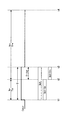
従来、二次電池の正極及び負極と入出力端子の正極及び負極との間をそれぞれ同極間で接続する充放電回路に、第1のFETと第2のFETが直列に接続された、電池保護装置が知られている(例えば、特許文献1参照)。図3は、特許文献1の図4に記載された電池保護装置の構成図である。図4は、特許文献1の図5に記載されたフローチャートである。この電池保護装置は、二次電池65の正極と負極間の電池電圧E1が充電禁止電圧以上であったとき(S2,Yes)、入出力端子の正極71と負極72間の端子電圧E2を検出して(S5)、端子電圧E2が電池電圧E1より高い充電状態が検出されているとき(S6,No)、第1及び第2のFET66,67をオフに制御して(S7)二次電池への充電を停止させるが、端子電圧E2が電池電圧E1より低い放電状態が検出されたとき(S6,Yes)、第1及び第2のFET66,67をオンに制御して(S4)放電を可能にしている(特許文献1の段落[0019]及び図5のフローチャート参照)。このように制御することによって、充電禁止の制御がなされている状態で放電が行われても、第1のFET66の寄生ダイオード66aに放電電流が流れないようにすることができるので、寄生ダイオード66aに放電電流が流れて発熱することによる劣化を防いでいる。
Conventionally, a battery in which a first FET and a second FET are connected in series to a charge / discharge circuit that connects between a positive electrode and a negative electrode of a secondary battery and a positive electrode and a negative electrode of an input / output terminal between the same electrodes. A protection device is known (see, for example, Patent Document 1). FIG. 3 is a configuration diagram of the battery protection device described in FIG. FIG. 4 is a flowchart described in FIG. This battery protection device detects a terminal voltage E2 between the
しかしながら、特許文献1の図5(本願の図4)によれば、電池電圧E1が充電禁止電圧以上である場合において(S2,Yes)、端子電圧E2が電池電圧E1より低い放電状態が検出されることにより(S6,Yes)第1及び第2のFET66,67をオン状態にした(S4)後は、端子電圧E2が電池電圧E1より高い充電状態が検出されない限り(S6)、第1及び第2のFET66,67をオフ状態(S7)にせずにオン状態(S4)に保持する制御を行うとしている。
However, according to FIG. 5 of Patent Document 1 (FIG. 4 of the present application), when the battery voltage E1 is equal to or higher than the charge prohibition voltage (S2, Yes), a discharge state in which the terminal voltage E2 is lower than the battery voltage E1 is detected. (S6, Yes) After the first and
ところが、第1及び第2のFET66,67がオンしている状態で端子電圧E2を検出しても(S5)、第1及び第2のFET66,67がオンしている以上、端子電圧E2と電池電圧E1はほぼ同電圧であるため、S6において、端子電圧E2が電池電圧E1より高い充電状態を検出する(すなわち、端子電圧E2と電池電圧E1との差を検出する)ことは容易ではない。したがって、電池電圧E1が充電禁止電圧以上である状況(S2,Yes)にもかかわらず、端子電圧E2が電池電圧E1より高い充電状態を検出して第1及び第2のFET66,67をオフ状態(S7)にすることにより二次電池65の充電を禁止状態にすることは非常に困難である。
However, even if the terminal voltage E2 is detected in a state where the first and
そこで、本発明は、二次電池の充電禁止条件が成立している状態で端子電圧が低下しても、端子電圧の低減を抑えつつ、二次電池の充電状態が継続することを防止することができる、電池保護装置及び電池パックの提供を目的とする。 Therefore, the present invention prevents the secondary battery from continuing to be charged while suppressing the reduction of the terminal voltage even if the terminal voltage is lowered while the charging prohibition condition for the secondary battery is satisfied. An object of the present invention is to provide a battery protection device and a battery pack.
上記目的を達成するため、本発明に係る電池保護装置は、
二次電池から電子機器への放電及び充電装置から前記二次電池への充電のための入出力端子と前記二次電池の両極端子との間の充放電経路の導通/遮断を切り替える切替手段と、
前記切替手段の切り替え動作を制御する制御手段とを備え、
前記制御手段は、前記二次電池の充電禁止条件が成立していることにより前記切替手段によって前記充放電経路を遮断している状態で前記入出力端子の端子電圧の低下が検出されると前記切替手段によって前記充放電経路を一時的に導通状態にする導通時間を設け、前記導通時間の経過時に前記切替手段によって前記充放電経路を遮断状態に戻すことを特徴とする。In order to achieve the above object, a battery protection device according to the present invention comprises:
Switching means for switching conduction / interruption of a charging / discharging path between the input / output terminal for discharging from the secondary battery to the electronic device and charging from the charging device to the secondary battery and the bipolar terminal of the secondary battery; ,
Control means for controlling the switching operation of the switching means,
The control means detects the decrease in the terminal voltage of the input / output terminal in a state where the charge / discharge path is blocked by the switching means due to the charging prohibition condition of the secondary battery being satisfied. The switching means is provided with a conduction time for temporarily turning on the charging / discharging path, and the switching means returns the charging / discharging path to a cut-off state when the conduction time elapses.
ここで、前記導通時間は、前記電子機器の動作態様の変化に同期した時間に設定されると好適である。例えば、前記電子機器は、無線通信機能を備えた携帯機器である。前記電子機器が無線通信機能を備えた携帯機器の場合、前記導通時間は、前記携帯機器の電波の送受信動作に同期した時間に設定されると好適である。 Here, it is preferable that the conduction time is set to a time synchronized with a change in the operation mode of the electronic device. For example, the electronic device is a portable device having a wireless communication function. When the electronic device is a portable device having a wireless communication function, it is preferable that the conduction time is set to a time synchronized with a radio wave transmission / reception operation of the portable device.
また、上記目的を達成するため、本発明に係る電池パックは、前記電池保護装置と前記二次電池とを内蔵する。 In order to achieve the above object, a battery pack according to the present invention incorporates the battery protection device and the secondary battery.
本発明によれば、二次電池の充電禁止条件が成立している状態で端子電圧が低下しても、端子電圧の低減を抑えつつ、二次電池の充電状態が継続することを防止することができる。 According to the present invention, even if the terminal voltage is lowered while the charging prohibition condition for the secondary battery is satisfied, the charging state of the secondary battery is prevented from continuing while suppressing the reduction of the terminal voltage. Can do.
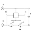
以下、図面を参照して、本発明を実施するための最良の形態の説明を行う。図1は、本発明の実施形態である電池パック100の全体構成図である。電池パック100は、リチウムイオン電池、ニッケル水素電池、電気二重層キャパシタなどの二次電池200を電源とする携帯機器300への放電及び二次電池200の充電器400による充電を行うための入出力端子5,6と二次電池200の両極端子3,4との間の充放電経路9(9a,9b)の導通/遮断を切り替えるスイッチング素子1,2と、スイッチング素子1,2の切り替え動作を制御する電池保護IC90とを備える電池保護装置を、二次電池200と共に内蔵するモジュール部品である。
The best mode for carrying out the present invention will be described below with reference to the drawings. FIG. 1 is an overall configuration diagram of a
電池パック100は、携帯機器300に、内蔵されたり、外付けされたりする。携帯機器300は、人が携帯可能な電子機器であって、携帯電話などの無線通信機能を備えるものが具体例として挙げられる。その他の具体例として、PDAやモバイルパソコン等の情報端末装置、カメラ、ゲーム機、音楽やビデオ等のプレーヤーなどが挙げられる。
The
スイッチング素子1,2は、二次電池200の負極4と負極入出力端子6との間の充放電経路9bの導通/遮断の切り替えが可能なように直列に接続される。スイッチング素子1は、充放電経路9を充電方向に流れる二次電池200の充電電流の遮断/導通を切り替え可能な第1の切替手段であり、スイッチング素子2は、充放電経路9を放電方向に流れる二次電池200の放電電流の遮断/導通を切り替え可能な第2の切替手段である。スイッチング素子1がオン状態で二次電池20の充電が許可され、オフ状態で二次電池200の充電が禁止される。また、スイッチング素子2がオン状態で二次電池200の放電が許可され、オフ状態で二次電池200の放電が禁止される。
スイッチング素子1,2は、例えば、寄生ダイオードを有するMOSFETやIGBTなどの半導体素子である。スイッチング素子1は、その寄生ダイオード1aの順方向が二次電池200の放電方向になる向きで負極4と負極入出力端子6との間に配置され、スイッチング素子2は、その寄生ダイオード2aの順方向が二次電池200の充電方向になる向きで負極4と負極入出力端子6との間に配置される。なお、スイッチング素子1,2は、バイポーラトランジスタであって、そのコレクタエミッタ間に図示の向きにダイオードが構成されたものでもよい。
The
電池保護IC90は、二次電池200の温度を検出する温度検出部10と、二次電池200の過充電を検出する過充電検出部などの電圧検出部21と、二次電池200の過放電を検出する過放電検出部22と、二次電池200の充放電電流を検出する電流検出部(例えば、充電時の過電流を検出する過電流検出部31と放電時の過電流を検出する過電流検出部32)と、各検出部からの検出結果を示す信号に基づいて、スイッチング素子1,2のオンオフを制御する制御部50とを備える。各検出部は、例えば、コンパレータやADコンバータによって構成されるとよい。制御部50は、例えば、論理回路やマイクロコンピュータによって構成されるとよい。
The battery protection IC 90 includes a
温度検出部10は、正側の充放電経路9aと負側の充放電経路9bとの間に直列に接続されたサーミスタ11と抵抗素子12との接続点の電圧を端子VTH1を介して検出することによって、二次電池200の温度を検出し、その検出した温度に応じた検出信号を制御部50に対して出力する。
The
電圧検出部21は、正側の充放電経路9aに接続されたVDD端子及び充放電経路9bのうち負側入出力端子6とスイッチング素子1との間の経路に接続されたV−端子を介して、正極入出力端子5と負極入出力端子6との端子間電圧を検出し、その検出した端子間電圧に応じた検出信号を制御部50に対して出力する。
The
制御部50は、二次電池200の充電禁止条件が成立している場合には、スイッチング素子1をオフする。これにより、スイッチング素子2のオンオフ状態にかかわらず、二次電池200を充電する充電電流が流れることを防止できる。また、二次電池200の放電禁止条件が成立している場合には、スイッチング素子2をオフする。これにより、スイッチング素子1のオンオフ状態にかかわらず、二次電池200の放電電流が流れることを防止できる。
The
二次電池200の充電禁止条件とは、例えば、二次電池200の温度、二次電池200に供給する充電電圧や充電電流、二次電池200の累積使用時間など、に基づいて定められている。
The charging prohibition condition of the
例えば、制御部50は、温度検出部10によって検出された二次電池200の温度が二次電池200の充電を禁止する温度範囲(例えば、所定の高温領域又は低温領域)内にある場合には(すなわち、二次電池200の充電を禁止する温度条件が成立している場合には)、スイッチング素子1をオフし、当該温度範囲外である場合には(当該温度条件が不成立の場合には)、スイッチング素子1をオンする。例えば、制御部50は、二次電池200の温度が二次電池200の充電を禁止する温度範囲内であることを表す信号が入力された場合にスイッチング素子1をオフにする信号を出力する回路で構成されるとよく、該温度範囲外であることを表す信号が入力された場合にスイッチング素子1をオンにする信号を出力する回路で構成されるとよい。これにより、特定の温度領域で充電されることによる二次電池200の劣化進行を遅らせることができる。
For example, when the temperature of the
また、例えば、制御部50は、電圧検出部21によって検出された二次電池200を充電するための充電電圧(すなわち、入出力端子5,6間の端子間電圧)が二次電池200の充電を禁止する電圧範囲(例えば、所定の高電圧領域)内である場合には(すなわち、二次電池200の充電を禁止する電圧条件が成立している場合には)、スイッチング素子1をオフし、当該電圧範囲外である場合には(当該電圧条件が不成立の場合には)、スイッチング素子1をオンする。これにより、特定の電圧領域で充電されることによる二次電池200の劣化進行を遅らせることができる。
Further, for example, the
なお、二次電池200の放電禁止条件に従ってスイッチング素子2のオンオフを制御する場合についても同様である。
The same applies to the case where on / off of the
ところで、スイッチング素子2がオンしている状態で、且つ、二次電池200の充電禁止条件が成立していることによりスイッチング素子1がオフしている状態において、携帯機器300と充電器400が共に入出力端子5,6に電気的に接続される場合がある。例えば、充電禁止条件が成立するような環境下で、携帯機器300が充電器400に接続されたまま動作しているような場合である。この場合、充電器400からの充電電流は、二次電池200には流れないが、携帯機器300には流れる。
By the way, in the state where the switching
しかしながら、携帯機器300の消費電流(負荷電流)が充電器400から供給される充電電流を上回る場合には、入出力端子5,6間の端子間電圧が下がる。この場合の端子間電圧は、二次電池200から携帯機器300に流れた放電電流が寄生ダイオード1aを経由することにより、少なくとも寄生ダイオード1aの順方向電圧分、二次電池200の両極端子3,4間の両極間電圧より低下する。このように端子間電圧が下がると、例えば、携帯機器300が、その端子間電圧の低下を検出することにより、電池パック100の異常と判断するおそれがある。また、寄生ダイオード1aに電流が流れることによって、発熱が生ずる。
However, when the consumption current (load current) of the
そこで、これらの問題を防ぐために、制御部50は、二次電池200の充電禁止条件の成立時にスイッチング素子1をオフすることにより充放電経路9を遮断している状態で端子間電圧の低下を示す検出信号が電圧検出部21から入力されると、スイッチング素子2をオンしたままスイッチング素子1をオフからオンに切り替えることにより充放電経路9を導通状態にする。電圧検出部21は、例えば、実際に検出された端子間電圧が、定常時の端子間電圧から寄生ダイオード1aの順方向電圧を差し引いた電圧値を下回る場合に、端子間電圧の低下を示す検出信号を制御部50に対して出力するとよい。端子間電圧の低下の検出感度を上げるため、実際に検出された端子間電圧が、定常時の端子間電圧から寄生ダイオード1aの順方向電圧より小さい電圧を差し引いた電圧値を下回る場合に、端子間電圧の低下を示す検出信号を制御部50に対して出力してもよい。
Therefore, in order to prevent these problems, the
このように、スイッチング素子2をオンしたままスイッチング素子1をオフからオンに切り替えることにより充放電経路9を導通状態にすることによって、寄生ダイオード1aを経由せずに二次電池200から携帯機器300への電力供給が可能となり、充電器400からだけでは補えない携帯機器300に必要な電力を二次電池200から補充することができ、端子間電圧の低下を防止しつつ、寄生ダイオード1aでの電圧降下による発熱防止を図ることができる。
In this way, by switching the
ところが、このようにスイッチング素子1のオンにより放電方向に充放電経路9を導通状態にしても携帯機器300の負荷電流が減少してくると、充電器400からだけで携帯機器300への電力供給を賄うことができ、充電器400からの充電電流は過剰となる結果、その過剰電流は二次電池200を充電する充電電流となってしまう。したがって、二次電池200の充電禁止条件が成立している状態であるにもかかわらず、スイッチング素子1がオンしていることにより、端子間電圧の低下抑制と寄生ダイオード1aでの発熱防止は図れるものの、二次電池200を充電状態にしてしまう。
However, when the load current of the
これを防ぐためには、オン状態にしたスイッチング素子1を再度オフ状態にすればよいが、スイッチング素子1がオン状態で端子間電圧を電圧検出部21によって検出しようとしても、スイッチング素子1,2がオンしている以上、二次電池200の電極間電圧と端子間電圧との間には電位差がほとんど生じないため、携帯機器300の負荷電流の減少による端子間電圧の低下からの復帰を端子間電圧の検出によって認識することは非常に困難である。
In order to prevent this, the switching
そこで、制御部50は、二次電池200の充電禁止条件の成立時にスイッチング素子1をオフすることにより充放電経路9を遮断している状態で端子間電圧の低下を示す検出信号が電圧検出部21から入力されると、スイッチング素子2をオンしたままスイッチング素子1をオフからオンに切り替えることにより充放電経路9を一時的に導通状態にする導通時間を設け、その導通時間の経過時にスイッチング素子1をオンからオフに切り替えることにより充放電経路9を遮断状態に戻す制御を行う。このように、スイッチング素子1のオンからオフへのタイミング(言い換えれば、充放電経路9の導通状態から遮断状態への切り替えタイミング)をスイッチング素子1のオンからの時間で時間管理することによって、端子間電圧の低下からの復帰を電圧検出により認識できなくても、スイッチング素子1をオンからオフに適切なタイミングで戻すことができる。
Therefore, the
そこで、制御部50は、一時的な導通時間を管理するため、時間管理手段としてタイマー51を備える。タイマー51は、スイッチング素子1のオン時点からの時間が予め決められた設定時間を経過した時にトリガー信号を生成するように構成される。制御部50は、二次電池200の充電禁止条件の成立時に端子間電圧の低下を示す検出信号が電圧検出部21から入力されることによりスイッチング素子1をオンした後、その設定時間の経過を示すトリガー信号がタイマー51によって生成されたときに、スイッチング素子1をオンからオフに戻す信号を出力する。
Therefore, the
スイッチング素子1の一時的なオン時間(すなわち、充放電経路9の一時的な導通時間)は、携帯機器300の動作態様の変化に同期した時間に設定されるとよい。携帯機器300の動作態様に応じてその負荷電流は変化するため、その動作態様の変化にスイッチング素子1のオン時間を同期させることで、二次電池200に必要以上に充放電させないようにすることができる。
The temporary ON time of the switching element 1 (that is, the temporary conduction time of the charging / discharging path 9) may be set to a time synchronized with a change in the operation mode of the
例えば、携帯機器300はその動作モードに応じて負荷電流は変化する。携帯機器300は、通常動作モードに対して消費電力が高い高消費電力モードで動作する場合がある。携帯機器300は、通常動作モードにおいて高消費電力モードの移行条件が成立すると、通常動作モードから高消費電力モードに移行する。また、携帯機器300は、高消費電力モードにおいて通常動作モードへの移行条件が成立すると、高消費電力モードから通常消費電力モードに移行する。携帯機器300が携帯電話であれば、電波環境の悪化を電波の受信レベルの低下等により検出すると、通常の送信電力より大きい送電電力で電波を送信する高消費電力モードに移行し、送受信動作を繰り返す。したがって、通常より大きい送信電力で電波を発信している発信時間の長さは予め定められているので、その発信時間に同期した時間にスイッチング素子1のオン時間の長さを設定することで、適切なタイミングで一時的にオン状態にしたスイッチング素子1をオフ状態に戻すことができる。スイッチング素子1のオン時間は、その発信時間以上の長さに設定するとよい。
For example, the load current of the
図2は、スイッチング素子1のオン時間と二次電池200の充放電電流との関係を示した図である。図2は、充電禁止条件が成立している環境下で充電器に接続された携帯電話が送受信している状況を示している。したがって、この状況では、携帯電話は、受信期間と通常より大きい送信電力で発信する発信期間とを繰り返して動作する。
FIG. 2 is a diagram showing the relationship between the on-time of the
Ttrは携帯電話の電波の発信期間であり、Itrは携帯電話の発信期間Ttrでの負荷電流であり、Trvは携帯電話の電波の受信期間であり、Irvは携帯電話の受信期間Trvでの負荷電流であり、Ichは充電器400が供給する充電電流、Tは充電禁止条件が成立している時に端子間電圧の低下が検出された場合のスイッチング素子1のオン時間である。
Ttr is a radio wave transmission period of the mobile phone, Itr is a load current during the mobile phone transmission period Ttr, Trv is a radio wave reception period of the mobile phone, and Irv is a load during the mobile phone reception period Trv. Ich is a charging current supplied by the
二次電池200に流入する電荷量Qchは、
Qch=(Ich−Irv)×(T−Ttr)+(Ich−Itr)×Ttr
・・・(1)
で表すことができる。The amount of charge Qch flowing into the
Qch = (Ich−Irv) × (T−Ttr) + (Ich−Itr) × Ttr
... (1)
Can be expressed as
二次電池200に流入する平均電流値Iは、
I={(Ich−Irv)×(T−Ttr)+(Ich−Itr)×Ttr}
/(Ttr+Trv) ・・・(2)
で表すことができる。The average current value I flowing into the
I = {(Ich−Irv) × (T−Ttr) + (Ich−Itr) × Ttr}
/ (Ttr + Trv) (2)
Can be expressed as
したがって、Itr>Ichの場合には、T=Ttrならば、電波の発信期間と受信期間とを合わせた1サイクルでの電池流入電流Iは負となり、二次電池200が放電していることを示す。
Therefore, in the case of Itr> Ich, if T = Ttr, the battery inflow current I in one cycle including the radio wave transmission period and the reception period is negative, and the
Itr>Ichになることにより端子間電圧が低下するので、その低下を検出したタイミングで、タイマー51のカウントCoutは1となり、一定時間Tの間保持する。携帯電話の発信期間での負荷電流Itrは受信期間での負荷電流Irvに比べ大きいため、発信期間Ttrでは、二次電池200から(Ich−Itr)の放電電流が流れる。そして、受信期間Trvに切り替わると、(Ich−Irv)の二次電池200を充電する充電電流が流れる。端子間電圧の低下を確実に防ぐため、TはTtr以上の時間に設定するとよい。しかし、二次電池200の充電が禁止されている状態での充電期間が長くならないように、端子間電圧の低下を防ぐための一時的な充電許可として、ばらつきを考慮してT−Ttrの長さができるだけ短くなるようなTを設定するとよい。
Since the voltage between the terminals decreases when Itr> Ich, the count Cout of the
したがって、充電禁止条件が成立している時に充電器が接続された携帯電話が微弱電波領域で動作している状況において、寄生ダイオードを流れる電流による発熱を防ぎつつ、端子間電圧の低下を抑制するために必要な期間だけ充放電経路9を導通状態にして、導通状態が継続することによって二次電池が充電されることを防ぐことができる。
Therefore, in the situation where the mobile phone to which the charger is connected is operating in the weak radio wave region when the charge prohibition condition is satisfied, the heat generation due to the current flowing through the parasitic diode is prevented and the decrease in the voltage between the terminals is suppressed. Therefore, it is possible to prevent the secondary battery from being charged by making the charging / discharging
以上、本発明の好ましい実施例について詳説したが、本発明は、上述した実施例に制限されることはなく、本発明の範囲を逸脱することなく、上述した実施例に種々の変形及び置換を加えることができる。 The preferred embodiments of the present invention have been described in detail above. However, the present invention is not limited to the above-described embodiments, and various modifications and substitutions can be made to the above-described embodiments without departing from the scope of the present invention. Can be added.
例えば、スイッチング素子1と2は、図1に示す配置位置を置換してもよい。
For example, the
本国際出願は、2008年9月25日に出願した日本国特許出願第2008−246650号に基づく優先権を主張するものであり、日本国特許出願第2008−246650号の全内容を本国際出願に援用する。 This international application claims priority based on Japanese Patent Application No. 2008-246650 filed on Sep. 25, 2008. The entire contents of Japanese Patent Application No. 2008-246650 are hereby incorporated by reference. Incorporated into.
1 充電制御用スイッチング素子
1a,2a 寄生ダイオード
2 放電制御用スイッチング素子
3 正極端子
4 負極端子
5 正側入出力端子
6 負側入出力端子
9a,9b 充放電経路
10 温度検出部
21 電圧検出部
50 制御部
51 タイマー
90 電池保護IC
100 電池パック
200 二次電池
300 携帯機器
400 充電器DESCRIPTION OF
100
Claims (4)
前記切替手段の切り替え動作を制御する制御手段とを備え、
前記制御手段は、前記二次電池の充電禁止条件が成立していることにより前記切替手段によって前記充放電経路を遮断している状態で前記入出力端子の端子電圧の低下が検出されると前記切替手段によって前記充放電経路を一時的に導通状態にする導通時間を設け、前記導通時間の経過時に前記切替手段によって前記充放電経路を遮断状態に戻すものであり、
前記導通時間は、前記電子機器の動作態様の変化に同期した時間に設定されることを特徴とする、電池保護装置。Switching means for switching conduction / interruption of a charging / discharging path between the input / output terminal for discharging from the secondary battery to the electronic device and charging from the charging device to the secondary battery and the bipolar terminal of the secondary battery; ,
Control means for controlling the switching operation of the switching means,
The control means detects the decrease in the terminal voltage of the input / output terminal in a state where the charge / discharge path is blocked by the switching means due to the charging prohibition condition of the secondary battery being satisfied. Providing a conduction time for temporarily turning on the charge / discharge path by a switching means, and returning the charge / discharge path to a cut-off state by the switching means when the conduction time has elapsed ;
The battery protection device according to claim 1, wherein the conduction time is set to a time synchronized with a change in an operation mode of the electronic device.
Priority Applications (1)
| Application Number | Priority Date | Filing Date | Title |
|---|---|---|---|
| JP2010530783A JP5110168B2 (en) | 2008-09-25 | 2009-08-20 | Battery protection device and battery pack incorporating the same |
Applications Claiming Priority (4)
| Application Number | Priority Date | Filing Date | Title |
|---|---|---|---|
| JP2008246650 | 2008-09-25 | ||
| JP2008246650 | 2008-09-25 | ||
| PCT/JP2009/064556 WO2010035595A1 (en) | 2008-09-25 | 2009-08-20 | Battery protection device and battery pack having the built-in battery protection device |
| JP2010530783A JP5110168B2 (en) | 2008-09-25 | 2009-08-20 | Battery protection device and battery pack incorporating the same |
Publications (2)
| Publication Number | Publication Date |
|---|---|
| JPWO2010035595A1 JPWO2010035595A1 (en) | 2012-02-23 |
| JP5110168B2 true JP5110168B2 (en) | 2012-12-26 |
Family
ID=42059602
Family Applications (1)
| Application Number | Title | Priority Date | Filing Date |
|---|---|---|---|
| JP2010530783A Active JP5110168B2 (en) | 2008-09-25 | 2009-08-20 | Battery protection device and battery pack incorporating the same |
Country Status (2)
| Country | Link |
|---|---|
| JP (1) | JP5110168B2 (en) |
| WO (1) | WO2010035595A1 (en) |
Cited By (1)
| Publication number | Priority date | Publication date | Assignee | Title |
|---|---|---|---|---|
| US10074875B2 (en) | 2013-11-25 | 2018-09-11 | Mitsumi Electric Co., Ltd. | Protection circuit for secondary battery, battery protection module, battery pack, and method |
Families Citing this family (1)
| Publication number | Priority date | Publication date | Assignee | Title |
|---|---|---|---|---|
| WO2017061161A1 (en) * | 2015-10-08 | 2017-04-13 | Connexx Systems株式会社 | Composite battery |
Citations (3)
| Publication number | Priority date | Publication date | Assignee | Title |
|---|---|---|---|---|
| JP2001057740A (en) * | 1999-08-18 | 2001-02-27 | Matsushita Electric Ind Co Ltd | Battery protecting device |
| JP2002034166A (en) * | 2000-07-19 | 2002-01-31 | Matsushita Electric Ind Co Ltd | Protective device for secondary battery |
| JP2008042964A (en) * | 2006-08-01 | 2008-02-21 | Fuji Electric Device Technology Co Ltd | Secondary battery protective device |
-
2009
- 2009-08-20 JP JP2010530783A patent/JP5110168B2/en active Active
- 2009-08-20 WO PCT/JP2009/064556 patent/WO2010035595A1/en active Application Filing
Patent Citations (3)
| Publication number | Priority date | Publication date | Assignee | Title |
|---|---|---|---|---|
| JP2001057740A (en) * | 1999-08-18 | 2001-02-27 | Matsushita Electric Ind Co Ltd | Battery protecting device |
| JP2002034166A (en) * | 2000-07-19 | 2002-01-31 | Matsushita Electric Ind Co Ltd | Protective device for secondary battery |
| JP2008042964A (en) * | 2006-08-01 | 2008-02-21 | Fuji Electric Device Technology Co Ltd | Secondary battery protective device |
Cited By (1)
| Publication number | Priority date | Publication date | Assignee | Title |
|---|---|---|---|---|
| US10074875B2 (en) | 2013-11-25 | 2018-09-11 | Mitsumi Electric Co., Ltd. | Protection circuit for secondary battery, battery protection module, battery pack, and method |
Also Published As
| Publication number | Publication date |
|---|---|
| JPWO2010035595A1 (en) | 2012-02-23 |
| WO2010035595A1 (en) | 2010-04-01 |
Similar Documents
| Publication | Publication Date | Title |
|---|---|---|
| US8314589B2 (en) | Battery pack | |
| KR101117037B1 (en) | Charge/discharge protection circuit, battery pack including charge/discharge protection circuit, and electronic device thereof | |
| US6563292B2 (en) | Charge/discharge protection circuit with latch circuit for protecting a charge control FET from overheating | |
| US8183835B2 (en) | Battery pack | |
| JP6041031B1 (en) | Secondary battery protection integrated circuit, secondary battery protection device and battery pack | |
| JP5811874B2 (en) | Battery protection circuit, battery protection device, and battery pack | |
| JP5891809B2 (en) | Battery protection circuit, battery protection device, and battery pack | |
| KR101387733B1 (en) | Battery pack, battery pack arrangement and electric apparatus | |
| JP2012254016A (en) | Overcharge detection circuit, battery pack and integrated circuit | |
| KR101982639B1 (en) | Complex integrated circuit for secondary battery, complex device for secondary battery and battery pack | |
| JP2013059212A (en) | Battery protection circuit, battery protection device and battery pack | |
| JP5334531B2 (en) | Pack battery | |
| JP2012208120A (en) | Semiconductor device for protection of secondary battery | |
| JP6221685B2 (en) | Secondary battery protection circuit, battery protection module, battery pack and processing method | |
| JP4546445B2 (en) | Rechargeable power supply device and semiconductor device | |
| JP5499702B2 (en) | Protection circuit, battery protection device, battery pack, and mode switching method | |
| JP5110168B2 (en) | Battery protection device and battery pack incorporating the same | |
| JP5338047B2 (en) | Battery pack | |
| JP2011239652A (en) | Battery protection device and integrated circuit for battery protection | |
| JP2009183050A (en) | Battery pack | |
| JP4626369B2 (en) | Battery unit | |
| JP2011015463A (en) | Protection circuit and protection method | |
| JP5397011B2 (en) | Protection circuit | |
| KR100898285B1 (en) | A battery pack for a portable electronic device | |
| JP6230181B2 (en) | Battery protection circuit and battery pack including the same |
Legal Events
| Date | Code | Title | Description |
|---|---|---|---|
| A131 | Notification of reasons for refusal |
Free format text: JAPANESE INTERMEDIATE CODE: A131 Effective date: 20120515 |
|
| A521 | Written amendment |
Free format text: JAPANESE INTERMEDIATE CODE: A523 Effective date: 20120605 |
|
| TRDD | Decision of grant or rejection written | ||
| A01 | Written decision to grant a patent or to grant a registration (utility model) |
Free format text: JAPANESE INTERMEDIATE CODE: A01 Effective date: 20120911 |
|
| A01 | Written decision to grant a patent or to grant a registration (utility model) |
Free format text: JAPANESE INTERMEDIATE CODE: A01 |
|
| A61 | First payment of annual fees (during grant procedure) |
Free format text: JAPANESE INTERMEDIATE CODE: A61 Effective date: 20120924 |
|
| FPAY | Renewal fee payment (event date is renewal date of database) |
Free format text: PAYMENT UNTIL: 20151019 Year of fee payment: 3 |
|
| R150 | Certificate of patent or registration of utility model |
Ref document number: 5110168 Country of ref document: JP Free format text: JAPANESE INTERMEDIATE CODE: R150 Free format text: JAPANESE INTERMEDIATE CODE: R150 |