JP5109982B2 - Manufacturing method of optical transmission body with mirror - Google Patents
Manufacturing method of optical transmission body with mirror Download PDFInfo
- Publication number
- JP5109982B2 JP5109982B2 JP2009003381A JP2009003381A JP5109982B2 JP 5109982 B2 JP5109982 B2 JP 5109982B2 JP 2009003381 A JP2009003381 A JP 2009003381A JP 2009003381 A JP2009003381 A JP 2009003381A JP 5109982 B2 JP5109982 B2 JP 5109982B2
- Authority
- JP
- Japan
- Prior art keywords
- reflection
- layer
- optical transmission
- mirror
- transmission body
- Prior art date
- Legal status (The legal status is an assumption and is not a legal conclusion. Google has not performed a legal analysis and makes no representation as to the accuracy of the status listed.)
- Expired - Fee Related
Links
Images


Classifications
-
- G—PHYSICS
- G02—OPTICS
- G02B—OPTICAL ELEMENTS, SYSTEMS OR APPARATUS
- G02B6/00—Light guides; Structural details of arrangements comprising light guides and other optical elements, e.g. couplings
- G02B6/10—Light guides; Structural details of arrangements comprising light guides and other optical elements, e.g. couplings of the optical waveguide type
- G02B6/12—Light guides; Structural details of arrangements comprising light guides and other optical elements, e.g. couplings of the optical waveguide type of the integrated circuit kind
- G02B6/122—Basic optical elements, e.g. light-guiding paths
-
- B—PERFORMING OPERATIONS; TRANSPORTING
- B29—WORKING OF PLASTICS; WORKING OF SUBSTANCES IN A PLASTIC STATE IN GENERAL
- B29C—SHAPING OR JOINING OF PLASTICS; SHAPING OF MATERIAL IN A PLASTIC STATE, NOT OTHERWISE PROVIDED FOR; AFTER-TREATMENT OF THE SHAPED PRODUCTS, e.g. REPAIRING
- B29C43/00—Compression moulding, i.e. applying external pressure to flow the moulding material; Apparatus therefor
- B29C43/02—Compression moulding, i.e. applying external pressure to flow the moulding material; Apparatus therefor of articles of definite length, i.e. discrete articles
- B29C43/021—Compression moulding, i.e. applying external pressure to flow the moulding material; Apparatus therefor of articles of definite length, i.e. discrete articles characterised by the shape of the surface
-
- B—PERFORMING OPERATIONS; TRANSPORTING
- B29—WORKING OF PLASTICS; WORKING OF SUBSTANCES IN A PLASTIC STATE IN GENERAL
- B29C—SHAPING OR JOINING OF PLASTICS; SHAPING OF MATERIAL IN A PLASTIC STATE, NOT OTHERWISE PROVIDED FOR; AFTER-TREATMENT OF THE SHAPED PRODUCTS, e.g. REPAIRING
- B29C70/00—Shaping composites, i.e. plastics material comprising reinforcements, fillers or preformed parts, e.g. inserts
- B29C70/68—Shaping composites, i.e. plastics material comprising reinforcements, fillers or preformed parts, e.g. inserts by incorporating or moulding on preformed parts, e.g. inserts or layers, e.g. foam blocks
- B29C70/74—Moulding material on a relatively small portion of the preformed part, e.g. outsert moulding
- B29C70/76—Moulding on edges or extremities of the preformed part
-
- B—PERFORMING OPERATIONS; TRANSPORTING
- B29—WORKING OF PLASTICS; WORKING OF SUBSTANCES IN A PLASTIC STATE IN GENERAL
- B29L—INDEXING SCHEME ASSOCIATED WITH SUBCLASS B29C, RELATING TO PARTICULAR ARTICLES
- B29L2011/00—Optical elements, e.g. lenses, prisms
-
- B—PERFORMING OPERATIONS; TRANSPORTING
- B29—WORKING OF PLASTICS; WORKING OF SUBSTANCES IN A PLASTIC STATE IN GENERAL
- B29L—INDEXING SCHEME ASSOCIATED WITH SUBCLASS B29C, RELATING TO PARTICULAR ARTICLES
- B29L2011/00—Optical elements, e.g. lenses, prisms
- B29L2011/0075—Light guides, optical cables
-
- Y—GENERAL TAGGING OF NEW TECHNOLOGICAL DEVELOPMENTS; GENERAL TAGGING OF CROSS-SECTIONAL TECHNOLOGIES SPANNING OVER SEVERAL SECTIONS OF THE IPC; TECHNICAL SUBJECTS COVERED BY FORMER USPC CROSS-REFERENCE ART COLLECTIONS [XRACs] AND DIGESTS
- Y10—TECHNICAL SUBJECTS COVERED BY FORMER USPC
- Y10T—TECHNICAL SUBJECTS COVERED BY FORMER US CLASSIFICATION
- Y10T156/00—Adhesive bonding and miscellaneous chemical manufacture
- Y10T156/10—Methods of surface bonding and/or assembly therefor
- Y10T156/1052—Methods of surface bonding and/or assembly therefor with cutting, punching, tearing or severing
- Y10T156/1062—Prior to assembly
- Y10T156/1066—Cutting to shape joining edge surfaces only
Landscapes
- Engineering & Computer Science (AREA)
- Physics & Mathematics (AREA)
- Mechanical Engineering (AREA)
- Microelectronics & Electronic Packaging (AREA)
- General Physics & Mathematics (AREA)
- Optics & Photonics (AREA)
- Chemical & Material Sciences (AREA)
- Composite Materials (AREA)
- Optical Integrated Circuits (AREA)
- Optical Elements Other Than Lenses (AREA)
Description
本発明は、コスト、量産性、信頼性に優れたミラー付き光伝送体の製造方法に関する。The present invention relates to a manufacturing method of an optical transmission body with a mirror excellent in cost, mass productivity, and reliability.
近年、インターネットに代表される情報通信技術の発達や情報処理装置の処理速度の飛躍的向上などに伴って、画像等の大容量データを送受信するニーズが高まりつつある。これら大容量データの伝送速度として、10Gbps以上の伝送速度が望まれており、さらに、電磁ノイズの影響が小さいことが望まれている。このような高速通信において、光を用いた通信技術に大きな期待が寄せられている。このため、従来一般的であった金属ケーブルや金属配線を用いた電気伝送から光ファイバや光導波路等の光伝送媒体を用いた光伝送へ移行しつつある。 In recent years, with the development of information communication technology represented by the Internet and the dramatic improvement in the processing speed of information processing apparatuses, there is an increasing need for transmitting and receiving large-capacity data such as images. As a transmission rate of these large-capacity data, a transmission rate of 10 Gbps or more is desired, and further, the influence of electromagnetic noise is desired to be small. In such high-speed communication, great expectations are placed on communication technology using light. For this reason, there is a shift from electrical transmission using a metal cable or metal wiring, which has been conventionally common, to optical transmission using an optical transmission medium such as an optical fiber or an optical waveguide.
光導波路を用いた光伝送では、実装時のコストメリットなどから、コアと平行な面上に光素子(面発光素子や面受光素子)が搭載された構造の光導波路が検討されている。 In optical transmission using an optical waveguide, an optical waveguide having a structure in which an optical element (a surface light-emitting element or a surface light-receiving element) is mounted on a surface parallel to a core has been studied from the viewpoint of cost merit at the time of mounting.
このとき、コアと光素子とを光学的に結合するためには、光路を約90°変換する必要があり、これを実現する手段として光導波路にダイシングなどによりV溝を形成し、そのV溝によるコアの斜面にミラーを作製する手段がある。例えば、光導波路に形成した斜面には何も付けず、空気と光導波路材料(コア材料)の屈折率差による全反射を利用してミラーを形成したり、上記斜面に金などの金属を蒸着して金属膜を形成することによりミラーを形成したりする。 At this time, in order to optically couple the core and the optical element, it is necessary to change the optical path by about 90 °. As a means for realizing this, a V-groove is formed in the optical waveguide by dicing or the like. There is a means to make a mirror on the slope of the core. For example, nothing is attached to the slope formed on the optical waveguide, and a mirror is formed using total reflection due to the difference in refractive index between air and the optical waveguide material (core material), or a metal such as gold is deposited on the slope. Then, a mirror is formed by forming a metal film.
光導波路の代わりに光ファイバを用いてもよく、基板に固定された光ファイバにダイシングなどによりV溝を形成し、そのV溝による光ファイバコアの斜面にミラーを作製することができる。以下、光導波路、光ファイバを総括して光伝送体と呼ぶ。 An optical fiber may be used instead of the optical waveguide, and a V-groove is formed in the optical fiber fixed to the substrate by dicing or the like, and a mirror can be produced on the slope of the optical fiber core by the V-groove. Hereinafter, the optical waveguide and the optical fiber are collectively referred to as an optical transmission body.
しかしながら、ダイシングなどにより作製したミラーには、表面に荒れ(凹凸)が有るため、反射効率が低下し、光の伝送損失が大きくなるという問題がある。特に、ダイシングの対象物が軟らかい材料であるとき、ダイシング面は荒れやすい。このため、フレキシブルな光導波路や光ファイバをダイシングで加工しようとすると、ダイシング面が顕著に荒れてしまう。 However, a mirror manufactured by dicing or the like has a problem that the surface has roughness (unevenness), so that the reflection efficiency is lowered and the light transmission loss is increased. In particular, when the object to be diced is a soft material, the dicing surface tends to be rough. For this reason, when it is going to process a flexible optical waveguide and an optical fiber by dicing, a dicing surface will become remarkably rough.
一方、金属を蒸着する方法においては、光導波路のサイズが大きくなると蒸着釜に入る数が限られるのでコストがかかり、また、金属の蒸着が不要な部分はマスクが必要であるためコスト高になり、さらにマスキングの解像度に限界がある。 On the other hand, in the method for depositing metal, if the size of the optical waveguide is increased, the number of entering the deposition pot is limited, which increases the cost. In addition, a mask is necessary for a portion that does not require deposition of metal, resulting in an increase in cost. Furthermore, the resolution of masking is limited.
また、蒸着で形成した金属膜と光導波路材料との接着性が悪く、剥がれやすいといった問題がある。 In addition, there is a problem in that the adhesion between the metal film formed by vapor deposition and the optical waveguide material is poor and is easily peeled off.
そこで、本発明の目的は、上記課題を解決し、コスト、量産性、信頼性に優れたミラー付き光伝送体の製造方法を提供することにある。An object of the present invention is to solve the above problems, cost, mass production is to provide a method for producing a reliability superior mirrored optical transmission member.
上記目的を達成するために本発明の要旨は、光伝送方向に連続的に形成されている光伝送層の途中にその光伝送方向に対して傾斜させてダイシングにより切削加工することによって、粗面を有するV溝を形成する第1のステップと、上記粗面に密着させて上記粗面を覆う未固化状態の反射補助層を形成する第2のステップと、固形の部材からなり上記V溝の傾斜に対応する傾斜角の平滑面を有する整形部材を用い、上記整形部材の平滑面を未固化状態の上記反射補助層に押し付けて、上記反射補助層に上記光伝送層からの光が反射される反射補助層の平滑面を形成する第3のステップと、未固化状態の上記反射補助層を固化する第4のステップと、を有することを特徴とするミラー付き光伝送体の製造方法である。
In order to achieve the above object, the gist of the present invention is that a rough surface is formed by inclining the optical transmission layer in the middle of the optical transmission layer continuously formed in the optical transmission direction and cutting by dicing. A first step of forming a V-groove having a second surface, a second step of forming a non-solidified reflection assisting layer that is in close contact with the rough surface and covers the rough surface, and a solid member made of the V-groove. Using a shaping member having a smooth surface with an inclination angle corresponding to the inclination, the smooth surface of the shaping member is pressed against the non-solidified reflection auxiliary layer, and the light from the light transmission layer is reflected on the reflection auxiliary layer. And a fourth step of solidifying the non-solidified reflection auxiliary layer. A method for producing an optical transmission body with a mirror, comprising: a third step of forming a smooth surface of the reflection auxiliary layer. .
本発明は次の如き優れた効果を発揮する。 The present invention exhibits the following excellent effects.
コスト、量産性、信頼性に優れたミラー付き光伝送体が製造できる。 An optical transmission body with a mirror excellent in cost, mass productivity, and reliability can be manufactured.
以下、本発明の一実施形態を添付図面に基づいて詳述する。 Hereinafter, an embodiment of the present invention will be described in detail with reference to the accompanying drawings.
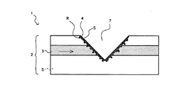
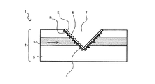
図1〜図6に示されるように、本発明に係るミラー付き光伝送体1は、光伝送体2の光が伝送される光伝送層3にその光伝送方向に対して交差する粗面Rが形成され、粗面Rに密着して粗面Rを覆う反射補助層4が形成され、反射補助層4に光伝送層3からの光が反射される平滑面Sが形成されているものである。この平滑面Sがミラーの反射面となる。このように、光伝送層3の光伝送方向延長上に平滑面Sを反射面とする反射補助層4が配置されることにより、光伝送方向を変換するミラーが形成される。
As shown in FIGS. 1 to 6, the
光伝送体2は、光伝送層3の光伝送方向を基板5に対して平行にして、基板5に搭載されている。ただし、図4〜図6のミラー付き光伝送体1では、光伝送体2と基板5が一体的に形成され光伝送体2の一部が基板5を兼ねているものを示してある。光伝送体2と基板5が別々に形成されたものでも、図4〜図6のミラー付き光伝送体1を構成することができる。
The
光伝送体2は、光導波路又は光ファイバである。光導波路は、矩形断面のコアの周囲をクラッドで囲んだものである。この場合、基板5上にクラッドとコアが積層形成される。光ファイバは、円形断面のコアの周囲を円形断面のクラッドで囲んだものである。この場合、基板5上に光ファイバが敷設される。いずれの場合も、側面図は、図1〜図6に示した通りであり、コアが光伝送層3となる。
The
図1〜図4に示されるミラー付き光伝送体1では、粗面Rは、光伝送層3の光伝送方向(図示左右方向)に対して直角に交差している。図1、図2の場合、基板5上に形成されている光伝送体2の端部がダイシング等により光伝送方向に対して直角に切削加工されたことにより、その切削面が粗面Rとなっている。図3、図4の場合、基板5上の光伝送方向に連続的に形成されている光伝送体2の途中がダイシング、レーザ加工等により光伝送方向に対して直角に切削加工されたことにより、角溝6が形成され、この角溝6の切削面が粗面Rとなっている。
なお、光伝送方向(図示左右方向)に対して直角に交差している反射補助層4を有する図1、図3のミラー付き光伝送体1は、光伝送方向(図示左右方向)に反射補助層4とは別のミラー(図示せず)を形成することにより、レーザ発振等の共振器としての利用が可能である。
In the
1 and 3 having the
図5、図6に示されるミラー付き光伝送体1では、粗面Rは、光伝送層3の光伝送方向に対して傾斜して交差している。基板5上の光伝送方向に連続的に形成されている光伝送体2の途中がV字状ブレードを用いたダイシング、レーザ加工等により光伝送方向に対して傾斜して切削加工されたことにより、V溝7が形成され、このV溝7の切削面が粗面Rとなっている。
In the
光伝送体2が硬い材質の場合、切削面は比較的滑らかにできる。一方、光伝送体2がフレキシブルな光導波路や樹脂製の光ファイバのように軟らかい材質の場合、切削面は顕著に荒れた粗面Rとなる。本発明は、光伝送体2の硬さには無関係に適用できるが、顕著に荒れた粗面Rにおける反射効率の低下を解消するという目的に特に有効である。例えば、光伝送体2の光伝送層3の弾性率が1GPa以下の場合に、特に有効である。
When the
反射補助層4は、透明な材料からなる。ここで透明とは、光伝送層3を伝送される特定波長の光、特定波長帯の光又は広波長帯域の光に対して伝送損失等の条件に適合できる程度に十分に高い透過率を示すということである。
The reflection
反射補助層4と光伝送層(コア)3の屈折率は、同一であることが理想的であるが、完璧に同一であることが必須というわけではない。反射補助層4と光伝送層3の屈折率差が大きくなればなるほど、光伝送層3を伝送されてきた光が反射補助層4との境界面で拡散しやすい。しかし、反射補助層4の屈折率は、光伝送層3の屈折率に対してかなり差があっても、光の拡散による伝送損失が深刻でなければ、問題ない。例えば、反射補助層4の屈折率が光伝送層3の屈折率に対して屈折率差±0.1以内であれば、光の拡散による伝送損失は十分に小さくできる。屈折率差が±0.1を超えたらただちに不可というわけでなく、反射補助層4の屈折率は、クラッドの屈折率と同程度でもよい。
The refractive index of the reflection
反射補助層4は、熱硬化樹脂又は光硬化樹脂で形成することができる。また、反射補助層4は、熱可塑性樹脂で形成することができる。これら、熱硬化樹脂、光硬化樹脂、熱可塑性樹脂は、一般に、接着剤と呼ばれるものである。具体的な、反射補助層4の形成方法は、後に述べる。
The reflection
図1、図3に示されるミラー付き光伝送体1では、反射補助層4の平滑面Sは、基板5に対して直角に形成されている。この場合、平滑面Sは、基板5に沿って伝送されてきた光を基板5に沿った方向に反射するミラーを構成する。
In the
図2、図4〜図6に示されるミラー付き光伝送体1では、反射補助層4の平滑面Sは、基板5に対して傾斜して形成されている。この場合、平滑面Sは、基板5に沿って伝送されてきた光を基板5に交差する方向に反射するミラーを構成する。平滑面Sの基板5に対する傾斜角が45°であれば、光の反射方向は基板5に直角となる。
In the
図6に示されるミラー付き光伝送体1は、反射補助層4の平滑面Sを覆う金属膜又は多層膜等からなる光反射膜8を備えている。これにより、ミラーは光反射膜付きミラーとなる。これに対し、図1〜図5に示されるミラー付き光伝送体1では、反射補助層4の平滑面S自体が光反射膜なしミラーを構成している。これは、反射補助層4の屈折率と空気の屈折率とに十分な差があるからである。図1〜図4のミラー付き光伝送体1においても、反射補助層4の平滑面Sを覆う光反射膜8を備えることができる。
The
次に、ミラー付き光伝送体1の製造方法を説明する。
Next, the manufacturing method of the
図7〜図15に示されるように、本発明のミラー付き光伝送体製造方法は、光伝送体2の光が伝送される光伝送層3にその光伝送方向に対して交差する粗面Rをダイシングにより形成する切削加工ステップP1と、粗面Rに密着させて粗面Rを覆う反射補助層4を形成する層追加ステップP2と、反射補助層4に光伝送層3からの光が反射される平滑面Sを形成する平滑化ステップP3とを有する。
As shown in FIGS. 7 to 15, the method for manufacturing a mirror-attached optical transmission body of the present invention has a rough surface R that intersects the
図7〜図12の製造方法においては、反射補助層4に平滑面Sを形成する平滑化ステップP3は、平滑面SSを有する整形部材9を用いて反射補助層4を整形する整形ステップP4を含む。整形部材9とは、未固化状態の反射補助層4に平滑面SSを押し付けることによって、反射補助層4に平滑面Sを形成する部材である。
7 to 12, the smoothing step P3 for forming the smooth surface S on the
図7〜図11の製造方法においては、反射補助層4に平滑面Sを形成する平滑化ステップP3は、整形部材9を反射補助層4から剥離させる離型ステップP5を含む。これとは異なり、図12の製造方法においては、離型ステップP5がなく、整形部材9が反射補助層4に接着された状態のままミラー付き光伝送体1に残る。
In the manufacturing method of FIGS. 7 to 11, the smoothing step P <b> 3 for forming the smooth surface S on the reflection
図13〜図15に示した製造方法においては、反射補助層4に平滑面Sを形成する平滑化ステップP3は、整形部材9の平滑面SSにあらかじめ光反射膜8を保持させる膜保持ステップP6と、光反射膜8を反射補助層4の平滑面Sに保持させる転写ステップP7と、光反射膜8から整形部材9を剥離させる剥離ステップP8とを含んでいる。
In the manufacturing method shown in FIGS. 13 to 15, the smoothing step P <b> 3 for forming the smooth surface S on the
以下、実施形態ごとに、詳しく説明する。 Hereinafter, each embodiment will be described in detail.
図7(a)に示されるように、光伝送体2は、光伝送層3の光伝送方向を基板5に対して平行にして基板5に搭載されている。切削加工ステップP1において、光伝送体2の端部がダイシング等により光伝送方向に対して直角に切削加工されたことにより、その切削面が粗面Rとなっている。層追加ステップP2では、未硬化状態の熱硬化樹脂、光硬化樹脂のいずれか、または熱可塑性樹脂からなる反射補助層材料を、粗面Rに対して隙間なく密着させ、反射補助層材料が粗面Rを覆うようにして、反射補助層4を形成する。この時点では、反射補助層4の粗面Rとは反対面は不定形であるが、平滑化ステップP3(整形ステップP4)では、そこへ整形部材9をあてがう。
As shown in FIG. 7A, the
整形部材9は、四角柱状(直方体状)に形成された固形の部材である。整形部材9は、金属、ガラス、プラスチックなどで形成される。プラスチックの場合、反射補助層4の反射補助層材料を整形、硬化させる熱、光などにより軟化しないことが好ましい。また、整形部材9は、反射補助層4からの剥離が容易なことが好ましい。整形部材9は、基板5に対して直角な平滑面SSを有する。整形部材9には、後に反射補助層4からの剥離を容易にするために、フッ素化合物などの剥離剤をあらかじめ付けておいてもよい。
The shaping
整形部材9の平滑面SSを反射補助層4の粗面Rとは反対面に押し当てると、反射補助層4が整形される。
When the smooth surface SS of the shaping
図7(b)に示されるように、反射補助層4が固化した後、離型ステップP5を行う。離型ステップP5では、整形部材9を反射補助層4から剥離させる。これにより、反射補助層4には、整形部材9の平滑面SSによって整形された平滑面Sが基板5に対して直角に形成され、図1のミラー付き光伝送体1が完成する。
As shown in FIG. 7B, after the
なお、整形部材9を物理的に剥離するのではなく、整形部材9を溶剤で溶解して除去してもよい。例えば、整形部材9をフッ酸で溶解するガラスで形成しておくと、反射補助層4が固化した後、整形部材9を溶解して除去する。また、整形部材9が可溶性プラスチックであれば、有機溶剤で溶解して除くことができる。
Instead of physically peeling the shaping
図8の製造方法は、図2のミラー付き光伝送体1を製造するためのものである。図7の製造方法と比べると、切削加工ステップP1において、光伝送方向に対して直角な粗面Rが形成される点は同じであるが、整形部材9が四角柱状でなく、平滑面SSが基板5に対して傾斜している。平滑化ステップP3において、この整形部材9を用いることにより、反射補助層4の平滑面Sは、基板5に対して傾斜して形成される。
The manufacturing method of FIG. 8 is for manufacturing the
図9(a)に示されるように、光伝送体2は、光伝送層3の光伝送方向を基板5に対して平行にして基板5に搭載されている。切削加工ステップP1において、基板5上の光伝送方向に連続的に形成されている光伝送体2の途中が光伝送方向に対して直角に切削加工されたことにより、角溝6が形成され、この角溝6の切削面が粗面Rとなっている。層追加ステップP2では、未固化状態の反射補助層材料を、粗面Rに対して隙間なく密着させ、反射補助層材料が粗面Rを覆うようにして、反射補助層4を形成する。平滑化ステップP3(整形ステップP4)では、四角柱状の整形部材9を角溝6に入れ、整形部材9の平滑面SSを反射補助層4の粗面Rとは反対面に押し当てることで、反射補助層4を整形する。
As shown in FIG. 9A, the
図9(b)に示されるように、反射補助層4が固化した後、離型ステップP5を行う。離型ステップP5では、整形部材9を反射補助層4から剥離させ、角溝6から排出する。これにより、反射補助層4には、整形部材9の平滑面SSによって整形された平滑面Sが基板5に対して直角に形成され、図3のミラー付き光伝送体1が完成する。
As shown in FIG. 9B, after the reflection
図10(a)に示されるように、光伝送体2は、光伝送層3の光伝送方向を基板5に対して平行にして基板5に搭載されている。切削加工ステップP1において、基板5上の光伝送方向に連続的に形成されている光伝送体2の途中が光伝送方向に対して直角に切削加工されたことにより、角溝6が形成され、この角溝6の切削面が粗面Rとなっている。層追加ステップP2では、未固化状態の反射補助層材料を、粗面Rに対して隙間なく密着させ、反射補助層材料が粗面Rを覆うようにして、反射補助層4を形成する。
As shown in FIG. 10A, the
平滑化ステップP3(整形ステップP4)では、平滑面SSが基板5に対して傾斜している整形部材9を角溝6に入れ、整形部材9の平滑面SSを反射補助層4の粗面Rとは反対面に押し当てることで、反射補助層4を整形する。
In the smoothing step P3 (shaping step P4), the shaping
図10(b)に示されるように、反射補助層4が固化した後、離型ステップP5を行う。離型ステップP5では、整形部材9を反射補助層4から剥離させ、角溝6から除去する。これにより、反射補助層4には、整形部材9の平滑面SSによって整形された平滑面Sが基板5に対して傾斜して形成され、図4のミラー付き光伝送体1が完成する。
As shown in FIG. 10B, after the
図11(a)に示されるように、光伝送体2は、光伝送層3の光伝送方向を基板5に対して平行にして基板5に搭載されている。切削加工ステップP1において、基板5上の光伝送方向に連続的に形成されている光伝送体2の途中が光伝送方向に対して傾斜させて切削加工されたことにより、V溝7が形成され、このV溝7の切削面が粗面Rとなっている。層追加ステップP2では、未硬化状態の熱硬化樹脂、光硬化樹脂のいずれか、または熱可塑性樹脂からなる反射補助層材料を、粗面Rに対して隙間なく密着させ、反射補助層材料が粗面Rを覆うようにして、反射補助層4を形成する。この時点では、反射補助層4の粗面Rの反対面は不定形である。
As shown in FIG. 11A, the
図11(b)に示されるように、平滑化ステップP3(整形ステップP4)では、反射補助層4に整形部材9を押し付ける。整形部材9は、基板5に対して45°の傾斜角に形成された平滑面SSを有することにより、反射補助層4に基板5に対する傾斜角が45°の平滑面Sを形成することができる。
As shown in FIG. 11B, in the smoothing step P3 (shaping step P4), the shaping
図11(c)に示されるように、反射補助層4が固化した後、離型ステップP5を行う。離型ステップP5では、整形部材9を反射補助層4から剥離させる。これにより、反射補助層4には、整形部材9の平滑面SSによって整形された平滑面Sが基板5に対して45°の傾斜角に形成され、図5のミラー付き光伝送体1が完成する。
As shown in FIG. 11C, after the
図12に示した製造方法では、V溝7の粗面Rに未固化状態の反射補助層材料を密着させ、整形部材9により反射補助層4を形成し、反射補助層4が固化すれば、ミラー付き光伝送体1が完成する。整形部材9はミラー付き光伝送体1に残る。整形部材9は、光に対し十分な反射率を持つことが好ましい。
In the manufacturing method shown in FIG. 12, the non-solidified reflection auxiliary layer material is adhered to the rough surface R of the
図13に示されるように、光伝送体2は、光伝送層3の光伝送方向を基板5に対して平行にして基板5に搭載されている。切削加工ステップP1において、基板5上の光伝送方向に連続的に形成されている光伝送体2の途中が光伝送方向に対して傾斜させて切削加工されたことにより、V溝7が形成され、このV溝7の切削面が粗面Rとなっている。
As shown in FIG. 13, the
図14(a)に示されるように、層追加ステップP2では、未硬化状態の熱硬化樹脂、光硬化樹脂のいずれか、または熱可塑性樹脂からなる反射補助層材料を、粗面Rに対して隙間なく密着させ、反射補助層材料が粗面Rを覆うようにして、反射補助層4を形成する。この時点では、反射補助層4の粗面Rの反対面は不定形である。
As shown in FIG. 14A, in the layer addition step P2, a reflection assisting layer material made of either an uncured thermosetting resin, a photocuring resin, or a thermoplastic resin is applied to the rough surface R. The
一方、整形部材9は、例えば、シリコンウエハから切り出された四角柱状(直方体状)に形成された固形の部材である。この整形部材9の平滑面SSに金属膜又は多層膜等からなる光反射膜8を付着させておく。金属膜材料には、例えば、金、銀、アルミニウムなどが挙げられる。
On the other hand, the shaping
図14(b)に示されるように、平滑化ステップP3(整形ステップP4)では、反射補助層4に整形部材9を押し付ける。整形部材9と反射補助層4との間に光反射膜8が挟まれる。この状態で、反射補助層4が固化すると、光反射膜8が反射補助層4に接着(固着)される。
As shown in FIG. 14B, in the smoothing step P3 (shaping step P4), the shaping
図15に示されるように、離型ステップP5では、整形部材9を反射補助層4から剥離させる。このとき、光反射膜8は、整形部材9から剥離されて反射補助層4に残る。これにより、図6のミラー付き光伝送体1が完成する。
As shown in FIG. 15, in the mold release step P <b> 5, the shaping
なお、図6のミラー付き光伝送体1の製造方法は、図13〜図15の製造方法に限らず、図5のミラー付き光伝送体1に対して金属膜蒸着、金属微粒子焼き付けなどにより、反射補助層4の平滑面Sに光反射膜8を形成してもよい。
In addition, the manufacturing method of the
以上説明したように、本発明に係るミラー付き光伝送体1は、切削加工で生じた粗面Rに密着して粗面Rを覆う反射補助層4が形成され、反射補助層4に光伝送層3からの光が反射される平滑面Sが形成されているため、この平滑面Sがミラーの反射面となる。ミラー付き光伝送体1は、金属蒸着やマスキングが不要であるため、生産コストが低減できると共に、量産性に優れる。また、ミラー付き光伝送体1は、反射補助層4に光伝送体と接着性の良いものを選ぶことができるため、蒸着膜に比べて剥がれにくく、信頼性に優れる。
特に、フレキシブルな光導波路や光ファイバをダイシングで切削加工すると粗面Rが顕著となるが、本発明は、このような軟らかい光伝送体2にミラーを形成する場合に好適である。
As described above, in the
In particular, when a flexible optical waveguide or optical fiber is cut by dicing, the rough surface R becomes conspicuous, but the present invention is suitable for forming a mirror on such a soft
柔軟性を求められる光導波路や光ファイバには、弾性率の低い材料が用いられることが多いが、低弾性率になるほど切削の際に平滑な面を形成しづらく、荒れた面となる。本発明は、特に弾性率が1GPa以下の部材を含む光伝送体に好適である。 A material having a low elastic modulus is often used for an optical waveguide or an optical fiber that requires flexibility, but the lower the elastic modulus, the more difficult it is to form a smooth surface during cutting, resulting in a rough surface. The present invention is particularly suitable for an optical transmission body including a member having an elastic modulus of 1 GPa or less.
図16に、本発明のミラー付き光伝送体の量産に適した製造方法を示す。基台161の上の複数箇所にミラーを形成する対象となる光伝送体162がそれぞれ保持されている。各光伝送体162には光伝送層(図示せず)を傾斜して切削したV溝163が形成されている。V溝163には反射補助層(図示せず)が形成されているものとする。 FIG. 16 shows a manufacturing method suitable for mass production of the optical transmission body with a mirror of the present invention. Optical transmission bodies 162 that are targets for forming mirrors are held at a plurality of locations on the base 161. Each optical transmission body 162 is formed with a V-groove 163 obtained by cutting an optical transmission layer (not shown) at an angle. It is assumed that a reflection auxiliary layer (not shown) is formed in the V groove 163.
基台161の上方に基台161に対向する昇降台164が昇降自在に設置されている。昇降台164には、基台161上の各光伝送体162に臨ませてジグ保持部165が設けられている。ジグ保持部165は、光伝送体162の反射補助層に平滑面を整形するためのジグ166を保持している。ジグ166は、図11、図14で説明した整形部材9である。光伝送体162の溝の形状に応じて図7等で説明した整形部材9をジグ166としてもよい。また、基台161は基板5であってもよく、基板5の複数箇所にミラーを形成する場合にも本製造方法は有効である。
A lifting table 164 facing the base 161 is installed above the base 161 so as to be movable up and down. The lifting platform 164 is provided with a jig holding portion 165 so as to face each optical transmission body 162 on the base 161. The jig holding unit 165 holds a jig 166 for shaping a smooth surface on the reflection auxiliary layer of the optical transmission body 162. The jig 166 is the shaping
この構成により、複数箇所における反射補助層の整形を一括して同時に行うことができる。このとき、各ジグ166が各光伝送体162のV溝163に一斉に押し込まれるので、各V溝163において力のバランスが左右均等になりやすい。このため、ジグ166が左右に傾くことが防止される。ジグ166が傾くと、反射補助層に形成される平滑面の角度が設計値である例えば45°と異なってしまうため、光の反射角度が直角からずれてしまうが、本製造方法によれば、ジグ166の傾きを無くして、平滑面の角度を設計値どおりに製造することができる。 With this configuration, the reflection auxiliary layers at a plurality of locations can be shaped simultaneously. At this time, since each jig 166 is pushed into the V-groove 163 of each optical transmission body 162 at the same time, the balance of force tends to be equal left and right in each V-groove 163. For this reason, the jig 166 is prevented from tilting left and right. When the jig 166 is inclined, the angle of the smooth surface formed in the auxiliary reflection layer is different from a design value of, for example, 45 °, so that the light reflection angle is deviated from a right angle. The inclination of the jig 166 can be eliminated, and the angle of the smooth surface can be manufactured as designed.
弾性率50MPaのエポキシ系クラッド(屈折率1.50)と弾性率約1GPaのエポキシ系コア(屈折率1.58)よりなるポリマ導波路をポリイミド基板上に作製した。このポリマ導波路に90°V字カットブレードを用いて10cmの間隔で2箇所ダイシングによりV溝を設けた。V溝は導波路側から切り、ポリイミド基板はダイシングされていない。 A polymer waveguide composed of an epoxy clad having an elastic modulus of 50 MPa (refractive index of 1.50) and an epoxy core having an elastic modulus of about 1 GPa (refractive index of 1.58) was produced on a polyimide substrate. V-grooves were formed in this polymer waveguide by dicing at two locations at intervals of 10 cm using a 90 ° V-shaped cutting blade. The V-groove is cut from the waveguide side, and the polyimide substrate is not diced.
比較例として、V溝に整形を施す前の状態で導波路の挿入損失を測定した。ポリイミド基板側より一方のV溝のミラー面にシングルモードファイバを用いて850nmの光を結合させた。入射光は、10cmのコアを伝搬し、反対側のミラー面から反射されポリイミド基板側へと出射される。この出射光をPD(Photodiode)で検出したところ、挿入損失は8.5〜9dBであった。ファイバとの結合損失、PDとの結合損失は0とした場合、導波路の伝送損失は0.1dB/cmであるため、ミラー1個の損失は4dB程度となる。 As a comparative example, the insertion loss of the waveguide was measured in a state before shaping the V groove. 850 nm light was coupled to the mirror surface of one V-groove from the polyimide substrate side using a single mode fiber. Incident light propagates through a 10 cm core, is reflected from the opposite mirror surface, and is emitted toward the polyimide substrate. When this emitted light was detected by PD (Photodiode), the insertion loss was 8.5 to 9 dB. If the coupling loss with the fiber and the coupling loss with the PD are set to 0, the transmission loss of the waveguide is 0.1 dB / cm, so the loss of one mirror is about 4 dB.
この場合のミラー面の平均粗さRaを測定した。コア部の膜厚方向は0.38〜0.55μm、切削方向は0.17〜0.5μmであり、より弾性率の低いクラッド部において平均粗さは大きい。コア部、クラッド部が平滑に切削されないことでミラー面の散乱損失が大きくなっている。 The average roughness Ra of the mirror surface in this case was measured. The film thickness direction of the core portion is 0.38 to 0.55 μm, the cutting direction is 0.17 to 0.5 μm, and the average roughness is large in the cladding portion having a lower elastic modulus. Since the core part and the cladding part are not cut smoothly, the scattering loss of the mirror surface is increased.
同じ導波路サンプルについてミラー面に整形と金反射膜の転写を行った。シリコンウエハを角柱状に切り出し、シリコンウエハの平滑面上に金を蒸着させた。この角柱を用いて、ミラー面の整形を行った。屈折率1.56のエポキシ系の熱硬化樹脂を適量それぞれのV溝に塗布し、シリコンウエハの角柱の平滑面上の金膜がミラーの反射面側となるように配置した。2つの角柱上には、それぞれ角柱を保持するジグが取り付けられており、2つのジグに橋渡しするように昇降台を載せ、その上から500gfの力を加えた。150℃で1時間加熱することで熱硬化樹脂を硬化させた。V溝より角柱を引き剥がすことで取り除くと、角柱上の金膜はV溝側に転写されていることが確認された。上と同様に挿入損失を測定すると、2.5〜3dB程度であり、ミラー1個あたり1dB以下の損失となっていることが確認された。 The same waveguide sample was shaped on the mirror surface and transferred with a gold reflective film. A silicon wafer was cut into a prismatic shape, and gold was deposited on the smooth surface of the silicon wafer. Using this prism, the mirror surface was shaped. An appropriate amount of an epoxy-based thermosetting resin having a refractive index of 1.56 was applied to each V-groove, and the gold film on the smooth surface of the prism of the silicon wafer was placed on the reflection surface side of the mirror. Jigs for holding the prisms were attached to the two prisms, respectively, and a lifting platform was placed so as to bridge the two jigs, and a force of 500 gf was applied from above. The thermosetting resin was cured by heating at 150 ° C. for 1 hour. It was confirmed that the gold film on the prism was transferred to the V-groove side when it was removed by peeling off the prism from the V-groove. When the insertion loss was measured in the same manner as above, it was about 2.5 to 3 dB, and it was confirmed that the loss was 1 dB or less per mirror.
1 ミラー付き光伝送体
2 光伝送体
3 光伝送層
4 反射補助層
5 基板
6 角溝
7 V溝
8 光反射膜
9 整形部材
R 粗面
S、SS 平滑面
DESCRIPTION OF
Claims (5)
上記粗面に密着させて上記粗面を覆う未固化状態の反射補助層を形成する第2のステップと、
固形の部材からなり上記V溝の傾斜に対応する傾斜角の平滑面を有する整形部材を用い、上記整形部材の平滑面を未固化状態の上記反射補助層に押し付けて、上記反射補助層に上記光伝送層からの光が反射される反射補助層の平滑面を形成する第3のステップと、
未固化状態の上記反射補助層を固化する第4のステップと、
を有することを特徴とするミラー付き光伝送体の製造方法。 A first step of forming a V-groove having a rough surface by inclining with respect to the light transmission direction in the middle of the light transmission layer continuously formed in the light transmission direction and cutting by dicing;
A second step of forming a non-solidified reflection assisting layer in close contact with the rough surface to cover the rough surface;
Using a shaping member made of a solid member and having a smooth surface with an inclination angle corresponding to the inclination of the V-groove, the smooth surface of the shaping member is pressed against the non-solidified reflection auxiliary layer, and the reflection auxiliary layer is A third step of forming a smooth surface of the auxiliary reflection layer in which light from the light transmission layer is reflected;
A fourth step of solidifying the non-solidified reflection assisting layer;
The manufacturing method of the optical transmission body with a mirror characterized by having.
請求項1記載のミラー付き光伝送体の製造方法。 A fifth step of separating the shaping member from the solidified reflection auxiliary layer,
The manufacturing method of the optical transmission body with a mirror of Claim 1.
上記第4のステップにおいて、上記反射補助層を固化する際に、上記光反射膜が上記反射補助層に接着され、
上記第5のステップにおいて、上記光反射膜は、上記整形部材から剥離されて、上記反射補助層の平滑面に接着された状態で残る、
請求項2記載のミラー付き光伝送体の製造方法。 In the third step, a light reflecting film is attached in advance to the smooth surface of the shaping member, and the light reflecting film attached to the shaping member is pressed against the non-solidified reflection auxiliary layer, and the reflection Forming a smooth surface of the auxiliary layer,
In the fourth step, when the reflection auxiliary layer is solidified, the light reflection film is adhered to the reflection auxiliary layer,
In the fifth step, the light reflecting film is peeled off from the shaping member and remains adhered to the smooth surface of the auxiliary reflection layer.
The manufacturing method of the optical transmission body with a mirror of Claim 2.
請求項1〜3いずれかに記載のミラー付き光伝送体の製造方法。 The reflection auxiliary layer is made of a thermosetting resin, a photocurable resin, or a thermoplastic resin.
The manufacturing method of the optical transmission body with a mirror in any one of Claims 1-3.
請求項3に記載のミラー付き光伝送体の製造方法。 The light reflecting film is made of a metal film or a multilayer film.
The manufacturing method of the optical transmission body with a mirror of Claim 3.
Priority Applications (3)
| Application Number | Priority Date | Filing Date | Title |
|---|---|---|---|
| JP2009003381A JP5109982B2 (en) | 2008-10-09 | 2009-01-09 | Manufacturing method of optical transmission body with mirror |
| US12/576,258 US8335415B2 (en) | 2008-10-09 | 2009-10-09 | Mirror-embedded light transmission medium and fabrication method of same |
| CN200910178990.7A CN101718889B (en) | 2008-10-09 | 2009-10-09 | Mirror-embedded light transmission medium and fabrication method of same |
Applications Claiming Priority (3)
| Application Number | Priority Date | Filing Date | Title |
|---|---|---|---|
| JP2008263042 | 2008-10-09 | ||
| JP2008263042 | 2008-10-09 | ||
| JP2009003381A JP5109982B2 (en) | 2008-10-09 | 2009-01-09 | Manufacturing method of optical transmission body with mirror |
Publications (3)
| Publication Number | Publication Date |
|---|---|
| JP2010113325A JP2010113325A (en) | 2010-05-20 |
| JP2010113325A5 JP2010113325A5 (en) | 2011-06-23 |
| JP5109982B2 true JP5109982B2 (en) | 2012-12-26 |
Family
ID=42098934
Family Applications (1)
| Application Number | Title | Priority Date | Filing Date |
|---|---|---|---|
| JP2009003381A Expired - Fee Related JP5109982B2 (en) | 2008-10-09 | 2009-01-09 | Manufacturing method of optical transmission body with mirror |
Country Status (3)
| Country | Link |
|---|---|
| US (1) | US8335415B2 (en) |
| JP (1) | JP5109982B2 (en) |
| CN (1) | CN101718889B (en) |
Families Citing this family (14)
| Publication number | Priority date | Publication date | Assignee | Title |
|---|---|---|---|---|
| US8905610B2 (en) | 2009-01-26 | 2014-12-09 | Flex Lighting Ii, Llc | Light emitting device comprising a lightguide film |
| US9651729B2 (en) | 2010-04-16 | 2017-05-16 | Flex Lighting Ii, Llc | Reflective display comprising a frontlight with extraction features and a light redirecting optical element |
| US9028123B2 (en) | 2010-04-16 | 2015-05-12 | Flex Lighting Ii, Llc | Display illumination device with a film-based lightguide having stacked incident surfaces |
| AU2012225244A1 (en) | 2011-03-09 | 2013-10-03 | Flex Lighting Ii, Llc | Light emitting device with adjustable light output profile |
| JP5950618B2 (en) * | 2012-02-24 | 2016-07-13 | キヤノン株式会社 | Method for forming light transmitting member and method for manufacturing imaging apparatus |
| US9690032B1 (en) | 2013-03-12 | 2017-06-27 | Flex Lighting Ii Llc | Lightguide including a film with one or more bends |
| US9566751B1 (en) * | 2013-03-12 | 2017-02-14 | Flex Lighting Ii, Llc | Methods of forming film-based lightguides |
| US11009646B2 (en) | 2013-03-12 | 2021-05-18 | Azumo, Inc. | Film-based lightguide with interior light directing edges in a light mixing region |
| CN104516055A (en) * | 2013-09-26 | 2015-04-15 | 上海美维科技有限公司 | Method for improving optical quality of optical waveguide cut surface |
| JP2016203376A (en) * | 2013-10-04 | 2016-12-08 | コニカミノルタ株式会社 | Method for producing film mirror |
| EP3363619B1 (en) * | 2017-02-21 | 2020-01-22 | Signify Holding B.V. | 3d printed luminaires using optical fibers |
| WO2020047340A1 (en) | 2018-08-30 | 2020-03-05 | Flex Lighting Ii, Llc | Film-based frontlight with angularly varying diffusion film |
| CN113678035A (en) | 2019-01-03 | 2021-11-19 | 阿祖莫公司 | Reflective display including light guide and light turning film that produce multiple illumination peaks |
| WO2021022307A1 (en) | 2019-08-01 | 2021-02-04 | Flex Lighting Ii, Llc | Lightguide with a light input edge between lateral edges of a folded strip |
Family Cites Families (20)
| Publication number | Priority date | Publication date | Assignee | Title |
|---|---|---|---|---|
| JPS50155243A (en) * | 1974-06-05 | 1975-12-15 | ||
| DE2938810A1 (en) * | 1979-09-25 | 1981-04-09 | Siemens AG, 1000 Berlin und 8000 München | DEVICE FOR INJECTING RADIATION IN AN OPTICAL WAVE GUIDE |
| DE4012747A1 (en) * | 1990-04-21 | 1991-10-24 | Bodenseewerk Geraetetech | METHOD FOR THE PRODUCTION OF FINE OPTICAL FRONT SURFACES ON WAVE LADDERS |
| KR100236432B1 (en) * | 1996-07-31 | 1999-12-15 | 미야즈 쥰이치로 | Optical deflector, process for productng the same, and blade for use in production of optical deflector |
| JP3753508B2 (en) | 1996-07-31 | 2006-03-08 | 日本電信電話株式会社 | Optical path conversion element manufacturing method and optical path conversion element manufacturing blade |
| US6952504B2 (en) * | 2001-12-21 | 2005-10-04 | Neophotonics Corporation | Three dimensional engineering of planar optical structures |
| US6058228A (en) * | 1997-10-06 | 2000-05-02 | Nec Research Institute, Inc. | Cost-effective side-coupling polymer fiber optics for optical interconnections |
| US6684007B2 (en) * | 1998-10-09 | 2004-01-27 | Fujitsu Limited | Optical coupling structures and the fabrication processes |
| TW451084B (en) * | 1999-06-25 | 2001-08-21 | Toppan Printing Co Ltd | Optical-electro wiring board, mounted board, and manufacturing method of optical-electro wiring board |
| CN1390311A (en) * | 1999-11-11 | 2003-01-08 | 光技术统合网株式会社 | Optical connector and optical transceiver |
| JP3762208B2 (en) * | 2000-09-29 | 2006-04-05 | 株式会社東芝 | Optical wiring board manufacturing method |
| JP2002258081A (en) * | 2001-02-28 | 2002-09-11 | Fujitsu Ltd | Optical wiring board, manufacturing method of the same, and multi-layer optical wiring |
| JP2003240997A (en) * | 2002-02-21 | 2003-08-27 | Fujitsu Ltd | Manufacturing method for optical integrated circuit having spatial reflection type structure |
| DE60324222D1 (en) * | 2002-06-07 | 2008-12-04 | Fujifilm Corp | Process for producing structured layers |
| CA2471963C (en) * | 2002-09-20 | 2012-07-10 | Toppan Printing Co., Ltd. | Optical waveguide and method of manufacturing the same |
| JP3887371B2 (en) * | 2003-11-27 | 2007-02-28 | インターナショナル・ビジネス・マシーンズ・コーポレーション | Optical transmission board, optical transmission board manufacturing method, and opto-electric integrated circuit |
| JP2006184773A (en) * | 2004-12-28 | 2006-07-13 | Mitsui Chemicals Inc | Optical waveguide and opto-electric hybrid substrate having the same |
| JP2007219143A (en) | 2006-02-16 | 2007-08-30 | Sumitomo Bakelite Co Ltd | Optical waveguide structure and electronic equipment |
| JP2007293108A (en) | 2006-04-26 | 2007-11-08 | Mitsumi Electric Co Ltd | Optical apparatus and its manufacturing method |
| JP5018254B2 (en) * | 2007-06-06 | 2012-09-05 | 日立電線株式会社 | Optical waveguide with mirror and manufacturing method thereof |
-
2009
- 2009-01-09 JP JP2009003381A patent/JP5109982B2/en not_active Expired - Fee Related
- 2009-10-09 US US12/576,258 patent/US8335415B2/en not_active Expired - Fee Related
- 2009-10-09 CN CN200910178990.7A patent/CN101718889B/en not_active Expired - Fee Related
Also Published As
| Publication number | Publication date |
|---|---|
| US8335415B2 (en) | 2012-12-18 |
| CN101718889A (en) | 2010-06-02 |
| US20100092143A1 (en) | 2010-04-15 |
| JP2010113325A (en) | 2010-05-20 |
| CN101718889B (en) | 2013-08-21 |
Similar Documents
| Publication | Publication Date | Title |
|---|---|---|
| JP5109982B2 (en) | Manufacturing method of optical transmission body with mirror | |
| JP5018254B2 (en) | Optical waveguide with mirror and manufacturing method thereof | |
| US6944377B2 (en) | Optical communication device and laminated optical communication module | |
| US8715542B2 (en) | Method of manufacturing optical waveguide | |
| US20110084047A1 (en) | Methods For Fabrication Of Large Core Hollow Waveguides | |
| JP2010535357A (en) | Photonic guide device | |
| US6631228B2 (en) | Adhesive-free bonding method of fiber attachment for polymer optical waveguide on polymer substrate | |
| JP4252968B2 (en) | Manufacturing method of optical waveguide unit | |
| JP2007183467A (en) | Optical waveguide with mirror and its manufacturing method | |
| JP2001188146A (en) | Optical coupling method and optical circuit | |
| JP4962265B2 (en) | Optical waveguide manufacturing method | |
| JP4290065B2 (en) | Optical module and manufacturing method thereof | |
| JP3973072B2 (en) | Metal-coated optical fiber, sleeve-coated metal-coated optical fiber, and method of manufacturing optical semiconductor module | |
| JP3858683B2 (en) | Multilayer optical wiring and manufacturing method thereof | |
| JP3907036B2 (en) | Metal-coated optical fiber, sleeve-coated metal-coated optical fiber, and optical semiconductor module | |
| JP2008046333A (en) | Optical transmission/reception module | |
| JP2012058683A (en) | Film optical waveguide and manufacturing method of the same | |
| JP2005164801A (en) | Optical waveguide film and its manufacturing method | |
| JP4133410B2 (en) | Manufacturing method of optical fiber array | |
| JP2003270461A (en) | Optical communication component, stack type optical communication module, and method for manufacturing the same | |
| JP2009103804A (en) | Optical waveguide and method of manufacturing the same | |
| JP2008197380A (en) | Multichannel optical path converting element and its manufacturing method | |
| JP4498978B2 (en) | Planar optical circuit assembly and manufacturing method thereof | |
| JP2010078670A (en) | Polymer optical waveguide and method of manufacturing the same | |
| JP2004302401A (en) | Optical path converting element and its manufacturing method, optical integrated circuit and its manufacturing method |
Legal Events
| Date | Code | Title | Description |
|---|---|---|---|
| A521 | Written amendment |
Free format text: JAPANESE INTERMEDIATE CODE: A523 Effective date: 20110415 |
|
| A621 | Written request for application examination |
Free format text: JAPANESE INTERMEDIATE CODE: A621 Effective date: 20110415 |
|
| A521 | Written amendment |
Free format text: JAPANESE INTERMEDIATE CODE: A523 Effective date: 20110415 |
|
| A131 | Notification of reasons for refusal |
Free format text: JAPANESE INTERMEDIATE CODE: A131 Effective date: 20120605 |
|
| A977 | Report on retrieval |
Free format text: JAPANESE INTERMEDIATE CODE: A971007 Effective date: 20120606 |
|
| A521 | Written amendment |
Free format text: JAPANESE INTERMEDIATE CODE: A523 Effective date: 20120730 |
|
| TRDD | Decision of grant or rejection written | ||
| A01 | Written decision to grant a patent or to grant a registration (utility model) |
Free format text: JAPANESE INTERMEDIATE CODE: A01 Effective date: 20120911 |
|
| A01 | Written decision to grant a patent or to grant a registration (utility model) |
Free format text: JAPANESE INTERMEDIATE CODE: A01 |
|
| A61 | First payment of annual fees (during grant procedure) |
Free format text: JAPANESE INTERMEDIATE CODE: A61 Effective date: 20120924 |
|
| FPAY | Renewal fee payment (event date is renewal date of database) |
Free format text: PAYMENT UNTIL: 20151019 Year of fee payment: 3 |
|
| R150 | Certificate of patent or registration of utility model |
Free format text: JAPANESE INTERMEDIATE CODE: R150 |
|
| S111 | Request for change of ownership or part of ownership |
Free format text: JAPANESE INTERMEDIATE CODE: R313111 |
|
| R350 | Written notification of registration of transfer |
Free format text: JAPANESE INTERMEDIATE CODE: R350 |
|
| LAPS | Cancellation because of no payment of annual fees |