JP5100066B2 - Imaging apparatus and imaging method - Google Patents
Imaging apparatus and imaging method Download PDFInfo
- Publication number
- JP5100066B2 JP5100066B2 JP2006241243A JP2006241243A JP5100066B2 JP 5100066 B2 JP5100066 B2 JP 5100066B2 JP 2006241243 A JP2006241243 A JP 2006241243A JP 2006241243 A JP2006241243 A JP 2006241243A JP 5100066 B2 JP5100066 B2 JP 5100066B2
- Authority
- JP
- Japan
- Prior art keywords
- long
- time exposure
- short
- exposure
- read
- Prior art date
- Legal status (The legal status is an assumption and is not a legal conclusion. Google has not performed a legal analysis and makes no representation as to the accuracy of the status listed.)
- Expired - Fee Related
Links
Images


Classifications
-
- H—ELECTRICITY
- H04—ELECTRIC COMMUNICATION TECHNIQUE
- H04N—PICTORIAL COMMUNICATION, e.g. TELEVISION
- H04N23/00—Cameras or camera modules comprising electronic image sensors; Control thereof
- H04N23/70—Circuitry for compensating brightness variation in the scene
- H04N23/73—Circuitry for compensating brightness variation in the scene by influencing the exposure time
-
- H—ELECTRICITY
- H04—ELECTRIC COMMUNICATION TECHNIQUE
- H04N—PICTORIAL COMMUNICATION, e.g. TELEVISION
- H04N25/00—Circuitry of solid-state image sensors [SSIS]; Control thereof
- H04N25/50—Control of the SSIS exposure
- H04N25/53—Control of the integration time
- H04N25/533—Control of the integration time by using differing integration times for different sensor regions
-
- H—ELECTRICITY
- H04—ELECTRIC COMMUNICATION TECHNIQUE
- H04N—PICTORIAL COMMUNICATION, e.g. TELEVISION
- H04N25/00—Circuitry of solid-state image sensors [SSIS]; Control thereof
- H04N25/50—Control of the SSIS exposure
- H04N25/57—Control of the dynamic range
- H04N25/58—Control of the dynamic range involving two or more exposures
- H04N25/581—Control of the dynamic range involving two or more exposures acquired simultaneously
- H04N25/583—Control of the dynamic range involving two or more exposures acquired simultaneously with different integration times
-
- H—ELECTRICITY
- H04—ELECTRIC COMMUNICATION TECHNIQUE
- H04N—PICTORIAL COMMUNICATION, e.g. TELEVISION
- H04N25/00—Circuitry of solid-state image sensors [SSIS]; Control thereof
- H04N25/50—Control of the SSIS exposure
- H04N25/57—Control of the dynamic range
- H04N25/58—Control of the dynamic range involving two or more exposures
- H04N25/581—Control of the dynamic range involving two or more exposures acquired simultaneously
- H04N25/585—Control of the dynamic range involving two or more exposures acquired simultaneously with pixels having different sensitivities within the sensor, e.g. fast or slow pixels or pixels having different sizes
-
- H—ELECTRICITY
- H04—ELECTRIC COMMUNICATION TECHNIQUE
- H04N—PICTORIAL COMMUNICATION, e.g. TELEVISION
- H04N25/00—Circuitry of solid-state image sensors [SSIS]; Control thereof
- H04N25/50—Control of the SSIS exposure
- H04N25/57—Control of the dynamic range
- H04N25/58—Control of the dynamic range involving two or more exposures
- H04N25/587—Control of the dynamic range involving two or more exposures acquired sequentially, e.g. using the combination of odd and even image fields
- H04N25/589—Control of the dynamic range involving two or more exposures acquired sequentially, e.g. using the combination of odd and even image fields with different integration times, e.g. short and long exposures
Description
本発明は、ビデオカメラ等に用いられる撮像装置に関し、特にダイナミックレンジを拡大する技術に関するものである。 The present invention relates to an imaging apparatus used for a video camera or the like, and more particularly to a technique for expanding a dynamic range.
従来、CCDなどの個体撮像素子から露光量の異なる画像信号を得て、ダイナミックレンジを拡大する撮像装置が知られている(例えば特許文献1参照)。従来の撮像装置では、フィルタを設けた画素(フォトダイオード)とフィルタを設けない画素(フォトダイオード)が一行おきに配置されている。 2. Description of the Related Art Conventionally, there has been known an imaging device that obtains image signals having different exposure amounts from an individual imaging element such as a CCD and expands a dynamic range (see, for example, Patent Document 1). In a conventional imaging device, a pixel (photodiode) provided with a filter and a pixel (photodiode) provided with no filter are arranged every other row.
この従来の撮像装置は、フィルタを用いて画素の感度に差を設けることにより、画素の露光量が異なるように構成されており、1度の露光でも露光量の異なる画像信号が得られる。そして、このようにして得られた露光量の異なる画像信号を合成して、画像信号のダイナミックレンジを拡大する。
従来の撮像装置においては、ダイナミックレンジを拡大するために、フィルタを用いて画素の感度に差を設けて、画素の露光量が異なるように構成している。そのため、フィルタを設けた画素とフィルタを設けない画素の露光量の比を変えるためには、フィルタの交換を行わなければならない。つまり、従来の撮像装置では、画素の露光量の比を変えるのが困難であるという問題があった。したがって、明暗の差の大きい被写体を撮影するときに、被写体の明暗の差の度合いに応じて、画素の露光量の比を調整することが困難であるという問題があった。例えば、撮像装置を監視カメラ等として用いた場合に、明暗の差の大きい被写体を撮影するのに不向きであるという問題があった。 In the conventional imaging apparatus, in order to expand the dynamic range, a difference is provided in the sensitivity of the pixel using a filter so that the exposure amount of the pixel is different. For this reason, in order to change the ratio of the exposure amount of a pixel provided with a filter and a pixel provided with no filter, the filter must be replaced. That is, the conventional imaging apparatus has a problem that it is difficult to change the ratio of the exposure amounts of pixels. Therefore, when photographing a subject having a large difference in light and darkness, there is a problem that it is difficult to adjust the ratio of pixel exposure amounts in accordance with the degree of light and dark difference of the subject. For example, when the imaging device is used as a surveillance camera or the like, there is a problem that it is not suitable for photographing a subject having a large difference in brightness.
本発明は、上記従来の問題を解決するためになされたもので、画素グループごとに露光時間の調整が可能であり、被写体の明暗の差の度合いに応じてダイナミックレンジを拡大することのできる撮像装置を提供することを目的とする。 The present invention has been made to solve the above-described conventional problems, and can adjust the exposure time for each pixel group and can expand the dynamic range in accordance with the degree of difference in brightness of the subject. An object is to provide an apparatus.
本発明の撮像装置は、全画素が長時間露光画素グループと短時間露光画素グループに分割され、各画素グループの画素から所定のフレーム期間内において異なる露光時間の蓄積電荷信号を読出し可能な撮像手段と、前記フレーム期間内において長時間露光期間が経過した後の第1の読出しタイミングで、前記長時間露光画素グループから長時間露光の蓄積電荷信号を読み出す第1の読出し手段と、前記フレーム期間内において短時間露光期間が経過した後の第2の読出しタイミングで、前記短時間露光画素グループから短時間露光の蓄積電荷信号を読み出す第2の読出し手段と、前記第1の読出しタイミングおよび前記第2の読出しタイミングをそれぞれ独立に調整する読出しタイミング調整手段と、前記長時間露光画素グループから読み出した前記長時間露光の蓄積電荷信号を用いて、長時間露光信号を生成する長時間露光信号生成手段と、前記短時間露光画素グループから読み出した前記短時間露光の蓄積電荷信号を用いて、短時間露光信号を生成する短時間露光信号生成手段と、前記長時間露光信号と前記短時間露光信号を合成して、全画素分の映像信号を生成する合成手段と、を備えた構成を有している。 The imaging apparatus according to the present invention is an imaging unit in which all pixels are divided into a long-exposure pixel group and a short-exposure pixel group, and an accumulated charge signal having a different exposure time can be read from pixels of each pixel group within a predetermined frame period A first readout means for reading out a long-exposure accumulated charge signal from the long-exposure pixel group at a first readout timing after a long exposure period has elapsed within the frame period; and within the frame period In the second reading timing after the short exposure period elapses, second reading means for reading the short-time exposure accumulated charge signal from the short-time exposure pixel group, the first reading timing and the second reading timing Read timing adjustment means for independently adjusting the read timing of each, and reading from the long exposure pixel group The long-time exposure signal generation means for generating a long-time exposure signal using the accumulated charge signal of the long-time exposure and the short-time exposure accumulated charge signal read from the short-time exposure pixel group A short exposure signal generating means for generating a time exposure signal; and a combining means for generating a video signal for all pixels by combining the long exposure signal and the short exposure signal. ing.
この構成により、第1の読出しタイミングを変えることにより、長時間露光画素グループの画素の露光時間(長時間露光期間)を容易に変えることができる。また、第2の読出しタイミングを変えることにより、短時間露光画素グループの画素の露光時間(短時間露光期間)を容易に変えることができる。このように、第1の読出しタイミングと第2の読出しタイミングをそれぞれ調整することにより、画素グループごとに露光時間を調整することができ、被写体の明暗の差の度合いに応じてダイナミックレンジを拡大することができる。例えば、明暗の差の大きい被写体を撮影するときには、長時間露光期間を長くして短時間露光期間を短くするように調整することにより、ダイナミックレンジを拡大することができる。 With this configuration, the exposure time (long exposure period) of the pixels of the long exposure pixel group can be easily changed by changing the first readout timing. Further, by changing the second readout timing, it is possible to easily change the exposure time (short exposure period) of the pixels of the short exposure pixel group. In this way, by adjusting the first readout timing and the second readout timing, respectively, the exposure time can be adjusted for each pixel group, and the dynamic range is expanded according to the degree of difference in brightness of the subject. be able to. For example, when shooting a subject with a large difference in brightness, the dynamic range can be expanded by adjusting the long exposure period to be short and the short exposure period to be short.
また、本発明の撮像装置は、前記フレーム期間内における前記第1の読出しタイミングで、前記短時間露光画素グループから長時間露光の蓄積電荷信号を読み出す第3の読出し手段を備え、前記長時間露光信号作成手段は、前記短時間露光画素グループから読み出した前記長時間露光の蓄積電荷信号を、前記長時間露光画素グループから読み出した前記長時間露光の蓄積電荷信号に加算して、前記長時間露光信号を生成する構成を有している。 The image pickup apparatus of the present invention further includes third reading means for reading a long-time exposure accumulated charge signal from the short-time exposure pixel group at the first read-out timing within the frame period, and the long-time exposure. The signal generating means adds the long-exposure accumulated charge signal read from the short-exposure pixel group to the long-exposure accumulated charge signal read from the long-exposure pixel group, so that the long-exposure It has a configuration for generating a signal.
この構成により、長時間露光画素グループから読み出した長時間露光の蓄積電荷信号だけでなく、短時間露光画素グループから読み出した長時間露光の蓄積電荷信号を利用することができ、長時間露光信号の感度が向上する。 With this configuration, not only the long-exposure accumulated charge signal read from the long-exposure pixel group but also the long-exposure accumulated charge signal read from the short-exposure pixel group can be used. Sensitivity is improved.
また、本発明の撮像装置は、前記フレーム期間内における第2の読出しタイミングで、前記長時間露光画素グループから短時間露光の蓄積電荷信号を読み出す第4の読出し手段を備え、前記長時間露光信号作成手段は、前記長時間露光画素グループから読み出した前記短時間露光の蓄積電荷信号を、前記長時間露光画素グループから読み出した前記長時間露光の蓄積電荷信号に加算して、前記長時間露光信号を生成する構成を有している。 The image pickup apparatus of the present invention further includes a fourth readout unit that reads out a short-time exposure accumulated charge signal from the long-time exposure pixel group at a second readout timing within the frame period, and the long-time exposure signal. The creating means adds the short-time exposure accumulated charge signal read from the long-time exposure pixel group to the long-time exposure accumulated charge signal read from the long-time exposure pixel group, and Is generated.
この構成により、長時間露光画素グループから読み出した長時間露光の蓄積電荷信号だけでなく、長時間露光画素グループから読み出した短時間露光の蓄積電荷信号を利用することができ、長時間露光信号の感度がさらに向上する。 With this configuration, not only the long-exposure accumulated charge signal read from the long-exposure pixel group but also the short-exposure accumulated charge signal read from the long-exposure pixel group can be used. Sensitivity is further improved.
また、本発明の撮像装置では、前記長時間露光画素グループの画素と前記短時間露光画素グループの画素は、縦方向または横方向に交互に配置された構成を有している。 In the imaging apparatus of the present invention, the pixels of the long exposure pixel group and the pixels of the short exposure pixel group are alternately arranged in the vertical direction or the horizontal direction.
この構成により、長時間露光画素グループの画素と短時間露光グループの画素が、縦方向または横方向に偏りなく配置される。したがって、全画素を二つの画素グループ(長時間露光画素グループと短時間露光グループ)に分割したときに、各画素グループに解像度の偏りが生じるのを抑えることができる。 With this configuration, the pixels of the long-time exposure pixel group and the pixels of the short-time exposure group are arranged without deviation in the vertical direction or the horizontal direction. Therefore, when all the pixels are divided into two pixel groups (long exposure pixel group and short exposure group), it is possible to suppress the occurrence of bias in resolution in each pixel group.
また、本発明の撮像装置では、前記長時間露光画素グループおよび前記短時間露光画素グループの各々において、画素配列がベイヤー配列となるように、前記画素が配置された構成を有している。 Further, the imaging apparatus of the present invention has a configuration in which the pixels are arranged so that the pixel arrangement is a Bayer arrangement in each of the long exposure pixel group and the short exposure pixel group.
この構成により、長時間露光画素グループや短時間露光画素グループから読み出した蓄積電荷信号がベイヤー配列信号となるので、これらの蓄積電荷信号から生成した長時間露光信号や短時間露光信号は一般的な信号処理(原色ベイヤー用の信号処理)で容易に画像処理を行うことができる。 With this configuration, the accumulated charge signal read from the long exposure pixel group or the short exposure pixel group becomes a Bayer array signal. Therefore, the long exposure signal and the short exposure signal generated from these accumulated charge signals are generally used. Image processing can be easily performed by signal processing (signal processing for primary color Bayer).
また、本発明の撮像装置では、前記第1の読出し手段は、前記長時間露光画素グループの各画素に接続する第1の転送路と、前記長時間露光画素グループの各画素から前記第1の転送路への読出し経路となる第1のゲート電極を備え、前記第2の読出し手段は、前記短時間露光画素グループの各画素に接続する第2の転送路と、前記短時間露光画素グループの各画素から前記第2の転送路への読出し経路となる第2のゲート電極を備え、前記読出しタイミング調整手段は、前記第1の読出しタイミングで前記第1のゲート電極にゲート電圧を印加し、前記第2の読出しタイミングで前記第2のゲート電極にゲート電圧を印加する構成を有している。 In the imaging apparatus according to the aspect of the invention, the first reading unit may include the first transfer path connected to each pixel of the long-time exposure pixel group and the first transfer path from each pixel of the long-time exposure pixel group. A first gate electrode serving as a readout path to the transfer path, wherein the second readout means includes: a second transfer path connected to each pixel of the short-time exposure pixel group; and the short-time exposure pixel group A second gate electrode serving as a readout path from each pixel to the second transfer path, wherein the readout timing adjustment unit applies a gate voltage to the first gate electrode at the first readout timing; A gate voltage is applied to the second gate electrode at the second read timing.
この構成により、第1の読出しタイミングで、第1のゲート電極にゲート電圧を印加すると、長時間露光画素グループの各画素から第1の転送路へ長時間露光の蓄積電荷信号が読み出される。また、第2の読出しタイミングで、第2のゲート電極にゲート電圧を印加すると、短時間露光画素グループの各画素から第2の転送路へ短時間露光の蓄積電荷信号が読み出される。このようにして、画素グループごとに露光時間を調整することができる。 With this configuration, when a gate voltage is applied to the first gate electrode at the first read timing, a long-exposure accumulated charge signal is read from each pixel of the long-exposure pixel group to the first transfer path. Further, when a gate voltage is applied to the second gate electrode at the second read timing, the short-time exposure accumulated charge signal is read from each pixel of the short-exposure pixel group to the second transfer path. In this way, the exposure time can be adjusted for each pixel group.
また、本発明の撮像装置では、前記第3の読出し手段は、前記短時間露光画素グループの各画素に接続する前記第1の転送路と、前記短時間露光画素グループの各画素から前記第1の転送路への読出し経路となる第3のゲート電極を備え、前記読出しタイミング調整手段は、前記第1の読出しタイミングで前記第3のゲート電極にゲート電圧を印加する構成を有している。 In the imaging apparatus according to the aspect of the invention, the third reading unit may include the first transfer path connected to each pixel of the short-time exposure pixel group and the first pixel from each pixel of the short-time exposure pixel group. A third gate electrode serving as a read path to the transfer path, and the read timing adjusting means applies a gate voltage to the third gate electrode at the first read timing.
この構成により、第1の読出しタイミングで、第3のゲート電極にゲート電圧を印加すると、短時間露光画素グループの各画素から第1の転送路へ長時間露光の蓄積電荷信号が読み出される。これにより、短時間露光画素グループから読み出した長時間露光の蓄積電荷信号を利用することができる。 With this configuration, when a gate voltage is applied to the third gate electrode at the first read timing, a long-exposure accumulated charge signal is read from each pixel of the short-exposure pixel group to the first transfer path. Thereby, the accumulated charge signal of the long exposure read from the short exposure pixel group can be used.
また、本発明の撮像装置では、前記第4の読出し手段は、前記長時間露光画素グループの各画素に接続する前記第1の転送路と、前記長時間露光画素グループの各画素から前記第1の転送路への読出し経路となる前記第1のゲート電極を備え、前記読出しタイミング調整手段は、前記第2の読出しタイミングで前記第1のゲート電極にゲート電圧を印加する構成を有している。 In the imaging apparatus according to the aspect of the invention, the fourth reading unit may include the first transfer path connected to each pixel of the long exposure pixel group and the first transfer path from each pixel of the long exposure pixel group. The first gate electrode serving as a read path to the transfer path is provided, and the read timing adjustment means applies a gate voltage to the first gate electrode at the second read timing. .
この構成により、第2の読出しタイミングで、第1のゲート電極にゲート電圧を印加すると、長時間露光画素グループの各画素から第1の転送路へ短時間露光の蓄積電荷信号が読み出される。これにより、長時間露光画素グループから読み出した短時間露光の蓄積電荷信号を利用することができる。 With this configuration, when a gate voltage is applied to the first gate electrode at the second read timing, the short-exposure accumulated charge signal is read from each pixel of the long-exposure pixel group to the first transfer path. This makes it possible to use the short-time exposure accumulated charge signal read from the long-exposure pixel group.
本発明は、全画素が二つの画素グループに分割されており各画素グループの画素から異なる露光時間の蓄積電荷信号を読出し可能な撮像手段と、長時間露光画素グループから長時間露光の蓄積電荷信号を読み出す第1の読出しタイミングと短時間露光画素グループから短時間露光の蓄積電荷信号を読み出す第2の読出しタイミングをそれぞれ独立に調整する読出しタイミング調整手段を設けることにより、画素グループごとに露光時間の調整が可能であり、被写体の明暗の差の度合いに応じてダイナミックレンジを拡大することができるという効果を有する撮像装置を提供することができるものである。 The present invention provides an image pickup means in which all the pixels are divided into two pixel groups and can read out stored charge signals of different exposure times from the pixels of each pixel group, and a long-exposure stored charge signal from the long exposure pixel group. By providing read timing adjustment means for independently adjusting the first read timing for reading out and the second read timing for reading out the short-time exposure accumulated charge signal from the short-exposure pixel group, the exposure time of each pixel group can be adjusted. It is possible to provide an imaging apparatus that can be adjusted and has an effect that the dynamic range can be expanded in accordance with the degree of difference in brightness of the subject.
以下、本発明の実施の形態の撮像装置および撮像方法について、図面を用いて説明する。本実施の形態では、監視カメラ等として用いられる撮像装置の場合を例示する。 Hereinafter, an imaging apparatus and an imaging method according to embodiments of the present invention will be described with reference to the drawings. In this embodiment, a case of an imaging device used as a surveillance camera or the like is illustrated.
(第1の実施の形態)
本発明の第1の実施の形態の撮像装置を図1〜図7に示す。図1は、本実施の形態の撮像装置の構成を示すブロック図である。図2は、本実施の形態の撮像素子1の構成を示すブロック図である。図3は、撮像素子1の主要な構成を示す説明図である。また、図4は、撮像素子1の画素配置を示す説明図である。
(First embodiment)
An imaging apparatus according to a first embodiment of the present invention is shown in FIGS. FIG. 1 is a block diagram illustrating a configuration of the imaging apparatus according to the present embodiment. FIG. 2 is a block diagram showing a configuration of the
まず、図1を参照して、撮像装置の構成について説明する。図1に示すように、撮像装置は、CCDやCMOSなどの撮像素子1と、撮像素子1の読出しタイミングの制御を行うタイミングパルス発生器2を備えている。ここでは、撮像素子1が、本発明の撮像手段に相当し、タイミングパルス発生器2が、本発明の読出しタイミング調整手段に相当する。
First, the configuration of the imaging apparatus will be described with reference to FIG. As shown in FIG. 1, the imaging apparatus includes an
撮像装置は、撮像素子1からの二つの出力信号(長時間露光信号と短時間露光信号)に後述する同時化の処理を施す時間軸変換器3と、時間軸変換器3からの出力信号(同時化された長時間露光信号と短時間露光信号)を合成して全画素分の映像信号を生成する合成回路4を備えている。時間軸変換器3は、長時間露光信号と短時間露光信号をそれぞれ書き込んで読み出すための二つのラインメモリ5を備えている。ここでは、合成回路4が、本発明の合成手段に相当する。
The imaging apparatus includes a
また、撮像装置は、映像信号のコントラストを強調するような階調補正処理を施す階調補正回路6と、映像信号を輝度信号と色差信号に分離してビデオ出力信号として出力する輝度色差信号作成回路7を備えている。
In addition, the imaging apparatus also includes a
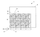
つぎに、図2〜図4を参照して、撮像素子1の構成について説明する。図2および図3に示すように、撮像素子1は、受光素子として複数のフォトダイオード8を備えている。撮像素子1の画素数は、このフォトダイオード8の総数によって決まる。そして、図3に示すように、このフォトダイオード8は、撮像素子1の基板9上に平面的に配置されており、長時間露光用のフォトダイオード8と短時間露光用のフォトダイオード8の二つのグループに分割されている。図3では、長時間露光用のフォトダイオード8が「L」で示されており、短時間露光用のフォトダイオード8が「S」で示されている。
Next, the configuration of the
画素とは、撮像素子1(CCD等)を構成する受光素子をいい、ここでは、フォトダイオード8が、本発明の画素に相当する。また、画素グループとは、画素のグループであり、ここでは、長時間露光用のフォトダイオード8のグループが、本発明の長時間露光画素グループに相当し、短時間露光用のフォトダイオード8のグループが、本発明の短時間露光画素グループに相当する。
The pixel refers to a light receiving element that constitutes the imaging element 1 (CCD or the like). Here, the
図3に示すように、長時間露光用のフォトダイオード8と短時間露光用のフォトダイオード8が、縦方向および横方向に交互に配置されている。すわなち、下から奇数行目(1行目、3行目、…)は長時間露光用のフォトダイオード8の行であり、下から偶数行目(2行目、4行目、…)は短時間露光用のフォトダイオード8の行である。また、左から奇数列目(1列目、3列目、…)は長時間露光用のフォトダイオード8の列であり、左から偶数列目(2列目、4列目、…)は短時間露光用のフォトダイオード8の列である。
As shown in FIG. 3, the long-
図3に示した撮像素子1では、下から奇数行目の長時間露光用のフォトダイオード8と、下から偶数行目の短時間露光用のフォトダイオード8が互いにずれた位置になるように、各フォトダイオード8が配置されている。また、左から奇数列目の長時間露光用のフォトダイオード8と、左から偶数列目の短時間露光用のフォトダイオード8が互いにずれた位置になるように、各フォトダイオード8が配置されている。
In the
また、本実施の形態の撮像素子1では、図4に示すように、長時間露光用のフォトダイオード8と短時間露光用のフォトダイオード8の各グループにおいて、画素配列がベイヤー配列となるように、各フォトダイオード8が配置されている。
Further, in the
つまり、下から奇数行目の長時間露光用のフォトダイオード8のグループについてみると、下から1行目の長時間露光用のフォトダイオード8の行では、G成分用のフォトダイオード8とB成分用のフォトダイオード8が交互に配置されており、下から3行目の長時間露光用のフォトダイオード8の行では、R成分用のフォトダイオード8とG成分用のフォトダイオード8が交互に配置されている。図4では、長時間用のG成分用のフォトダイオード8が「LG」で示されており、長時間用のB成分用のフォトダイオード8が「LB」で示されている。また、長時間用のR成分用のフォトダイオード8が「LR」で示されている。
In other words, regarding the group of the long-
同様に、下から偶数行目の短時間露光用のフォトダイオード8のグループについてみると、下から2行目の短時間露光用のフォトダイオード8の行では、G成分用のフォトダイオード8とB成分用のフォトダイオード8が交互に配置されており、下から4行目の短時間露光用のフォトダイオード8の行では、R成分用のフォトダイオード8とG成分用のフォトダイオード8が交互に配置されている。図4では、短時間用のG成分用のフォトダイオード8が「SG」で示されており、短時間用のB成分用のフォトダイオード8が「SB」で示されている。また、短時間用のR成分用のフォトダイオード8が「SR」で示されている。
Similarly, regarding the group of the short-
ここで、R成分用(またはG成分用、B成分用)のフォトダイオード8とは、R成分(またはG成分用、B成分用)の波長領域の感度が高いフォトダイオード8をいう。この場合、R成分、G成分、B成分の感度の異なるフォトダイオード8を、それぞれR成分用、G成分用、B成分用のフォトダイオード8として用いてもよい。また、感度特性が同じフォトダイオード8に、R成分、G成分、B成分の波長領域の透過率が高いカラーフィルタをそれぞれ設けて、R成分用、G成分用、B成分用のフォトダイオード8として用いてもよい。
Here, the R component (or G component, B component)
図2および図3に示すように、撮像素子1は、フォトダイオード8に蓄積された電荷(蓄積電荷)を垂直方向(縦方向、図3では下向き)に転送する二つの垂直転送路(第1垂直転送路10および第2垂直転送路11)と、垂直転送路から転送された電荷を水平方向(横方向、図3では左向き)に転送する水平転送路12を備えている。ここでは、蓄積電荷が、本発明の蓄積電荷信号に相当する。また、第1垂直転送路10が、本発明の第1の転送路に相当し、第2垂直転送路11が、本発明の第2の転送路に相当する。
As shown in FIGS. 2 and 3, the
撮像素子1は、長時間露光用のフォトダイオード8から第1垂直転送路10への読出し経路となる第1ゲート電極13と、短時間露光用のフォトダイオード8から第2垂直転送路11への読出し経路となる第2ゲート電極14を備えている。第1ゲート電極13は、タイミングパルス発生器2からゲート電圧が印加されると、長時間露光用のフォトダイオード8から第1垂直転送路10へ蓄積電荷を読み出すように制御されている。また、第2ゲート電極14は、タイミングパルス発生器2からゲート電圧が印加されると、短時間露光用のフォトダイオード8から第2垂直転送路11へ蓄積電荷を読み出すように制御されている。本実施の形態では、第1ゲート電極13にゲート電圧を印加する第1の読出しタイミングと、第2ゲート電極14にゲート電圧を印加する第2の読出しタイミングは、それぞれ独立に調整可能である。ここでは、第1ゲート電極13が、本発明の第1のゲート電極に相当し、第2ゲート電極14が、本発明の第2のゲート電極に相当する。そして、第1ゲート電極13と第1垂直転送路10が、本発明の第1の読出し手段に相当し、第2ゲート電極14と第2垂直転送路11が、本発明の第2の読出し手段に相当する。
The
図3に示した例では、左から奇数列目の長時間露光用のフォトダイオード8に対応する位置に、第1垂直転送路10が設けられており、左から偶数列目の短時間露光用のフォトダイオード8に対応する位置に、第2垂直転送路11が設けられている。そして、第1ゲート電極13によって、長時間露光用のフォトダイオード8と第1垂直転送路10が接続されており、第2ゲート電極14によって、短時間露光用のフォトダイオード8と第2垂直転送路11が接続されている。
In the example shown in FIG. 3, a first
そして、タイミングパルス発生器2から第1ゲート電極13にゲート電圧を印加するタイミング(第1の読出しタイミング)と、タイミングパルス発生器2から第2ゲート電極14にゲート電圧を印加するタイミング(第2の読出しタイミング)は、それぞれ独立に制御されている。このようにして、撮像素子1は、1フレーム期間内に異なる露光時間の蓄積電荷(長時間露光用のフォトダイオード8の蓄積電荷と短時間露光用のフォトダイオード8の蓄積電荷)をそれぞれ独立に読み出すことができるように構成されている。
Then, the timing at which the gate voltage is applied from the timing pulse generator 2 to the first gate electrode 13 (first reading timing), and the timing at which the gate voltage is applied from the timing pulse generator 2 to the second gate electrode 14 (second timing). Are read out independently. In this manner, the
また、図2および図3に示すように、撮像素子1は、第1垂直転送路10に読み出された蓄積電荷の電荷量に応じて長時間露光信号を生成する長時間露光信号生成部15と、第2垂直転送路11に読み出された蓄積電荷の電荷量に応じて短時間露光信号を生成する短時間露光信号生成部16を備えている。ここでは、長時間露光信号生成部15が、本発明の長時間露光信号生成手段に相当し、短時間露光信号生成部16が、本発明の短時間露光信号生成手段に相当する。
As shown in FIGS. 2 and 3, the
以上のように構成された撮像装置について、図5〜図7を用いてその動作を説明する。 About the imaging device comprised as mentioned above, the operation | movement is demonstrated using FIGS.
本発明の第1の実施の形態の撮像装置で被写体を撮影すると、撮像素子1のフォトダイオード8が入射光を受光し、光電効果によって電荷が蓄積される。図5には、フォトダイオード8の蓄積電荷量の時間変化の様子が示されている。図5に示すように、本実施の形態の撮像素子1では、1フレーム期間の開始時点において、タイミングパルス発生器2から基板電圧が印加され、すべてのフォトダイオード8(全画素)の残留電荷をリセットされる。そして、所定の長時間露光期間の間、フォトダイオード8に電荷が蓄積される。したがって、1フレーム期間の開始時点(1フレーム期間の開始時の全電荷リセットの時点)が、長時間露光期間の開始時点であるともいえる。
When a subject is photographed by the imaging apparatus according to the first embodiment of the present invention, the
そして、長時間露光期間が経過した後の第1の読出しタイミングで、タイミングパルス発生器2から第1ゲート電極13にゲート電圧が印加され、長時間露光用のフォトダイオード8の蓄積電荷が読み出される。この第1の読出しタイミングは、長時間露光期間の終了時点であるともいえる。本実施の形態では、第1の読出しタイミングで短時間露光用のフォトダイオード8の蓄積電荷の読出しは行わない。
A gate voltage is applied from the timing pulse generator 2 to the
その後、1フレーム期間中に、もう一度、タイミングパルス発生器2から基板電圧が印加され、すべてのフォトダイオード8(全画素)の残留電荷をリセットされる。そして、所定の短時間露光期間の間、フォトダイオード8に電荷が蓄積される。したがって、1フレーム期間中の全電荷リセットの時点が、短時間露光期間の開始時点であるともいえる。
Thereafter, during one frame period, the substrate voltage is applied again from the timing pulse generator 2 to reset the residual charges of all the photodiodes 8 (all pixels). Then, charges are accumulated in the
そして、短時間露光期間が経過した後の第2の読出しタイミングで、タイミングパルス発生器2から第2ゲート電極14にゲート電圧が印加され、短時間露光用のフォトダイオード8の蓄積電荷が読み出される。この第2の読出しタイミングは、1フレーム期間の終了時点であり、短時間露光期間の終了時点であるともいえる。本実施の形態では、第2の読出しタイミングで長時間露光用のフォトダイオード8の蓄積電荷の読出しは行わない。
Then, at the second read timing after the short exposure period has elapsed, the gate voltage is applied from the timing pulse generator 2 to the
図6には、フォトダイオード8から蓄積電荷が読み出され、撮像素子1から長時間露光信号と短時間露光信号が出力される様子が示されている。上記のようにして、第1の読出しタイミングで長時間露光用のフォトダイオード8から読み出された蓄積電荷は、第1ゲート電極13を介して第1垂直転送路10に読み出されて、第1垂直転送路10上に保持される。また、第2の読出しタイミングで短時間露光用のフォトダイオード8から読み出された蓄積電荷は、第2ゲート電極14を介して第2垂直転送路11に読み出されて、第2垂直転送路11上に保持される。
FIG. 6 shows a state in which the accumulated charge is read from the
そして、第1垂直転送路10と第2垂直転送路11にそれぞれ保持された蓄積電荷は、垂直方向(図6では下向き)に順次転送され、水平転送路12に読み出される。水平転送路12に読み出された蓄積電化は、水平方向(図6では左向き)に順次転送され、長時間露光信号と短時間露光信号として出力される。
The accumulated charges held in the first
このようにして、長時間露光信号生成部15は、長時間露光用のフォトダイオード8の蓄積電荷を用いて長時間露光信号を生成し、短時間露光信号生成部16は、短時間露光用のフォトダイオード8の蓄積電荷を用いて短時間露光信号を生成する。そして、生成された長時間露光信号と短時間露光信号は、撮像素子1から出力信号として出力され、増幅器17によって増幅される。この場合、撮像素子1からの出力信号は、1ライン(1行)ごとに長時間露光信号、短時間露光信号の順に出力される。
In this way, the long
図7は、撮像素子1から読み出された長時間露光信号と短時間露光信号に、時間軸変換器3が同時化の処理を施す様子を示す説明図である。時間軸変換器3では、長時間露光信号と短時間露光信号の時間軸を2倍にする(1/2速度にする)とともに、長時間露光信号と短時間露光信号の位相を一致させる同時化の処理が行われる。
FIG. 7 is an explanatory diagram illustrating a state in which the
具体的には、撮像素子1から1ラインごとに読み出された長時間露光信号と短時間露光信号を、それぞれ時間軸変換器3のラインメモリ5に書き込む。このとき、長時間露光信号と短時間露光信号は、読み出されたときのクロックレートで書き込まれる。そして、各ラインメモリ5に書き込まれた長時間露光信号と短時間露光信号を、1/2のクロックレートで読み出す。このとき、互いの位相が揃うようなタイミングで、長時間露光信号と短時間露光信号が読み出される。
Specifically, the long-time exposure signal and the short-time exposure signal read from the
そして、合成回路4で、同時化された長時間露光信号と短時間露光信号が合成されて、全画素分の映像信号が生成される。その後、階調補正回路6で、映像信号のコントラストを強調するような階調補正処理が施され、輝度色差信号作成回路7で、輝度信号と色差信号に分離されてビデオ出力信号として出力される。
Then, the synthesizing circuit 4 synthesizes the synchronized long exposure signal and the short exposure signal to generate a video signal for all the pixels. Thereafter, the
このような発明の第1の実施の形態の撮像装置によれば、すべてのフォトダイオード8が二つのグループ(長時間露光用のグループと短時間露光用のグループ)に分割されており、各グループのフォトダイオード8から異なる露光時間の蓄積電荷を読出し可能な撮像素子1と、長時間露光用のフォトダイオード8から長時間露光の蓄積電荷を読み出す第1の読出しタイミングと短時間露光用のフォトダイオード8から短時間露光の蓄積電荷を読み出す第2の読出しタイミングをそれぞれ独立に調整するタイミングパルス発生器2が設けられているので、フォトダイオード8のグループごとに露光時間の調整が可能であり、被写体の明暗の差の度合いに応じてダイナミックレンジを拡大することができる。
According to the imaging apparatus of the first embodiment of the invention, all the
すなわち、本実施の形態では、第1の読出しタイミングを変えることにより、長時間露光用のフォトダイオード8の露光時間(長時間露光期間)を容易に変えることができる。また、第2の読出しタイミングを変えることにより、短時間露光用のフォトダイオード8の露光時間(短時間露光期間)を容易に変えることができる。このように、第1の読出しタイミングと第2の読出しタイミングをそれぞれ調整することにより、フォトダイオード8のグループごとに露光時間を調整することができ、被写体の明暗の差の度合いに応じてダイナミックレンジを拡大することができる。例えば、明暗の差の大きい被写体を撮影するときには、長時間露光期間を長くして短時間露光期間を短くするように調整することにより、ダイナミックレンジを拡大することができる。
That is, in the present embodiment, the exposure time (long exposure period) of the
また、本実施の形態では、第1の読出しタイミングで、第1ゲート電極13にゲート電圧を印加すると、長時間露光用のフォトダイオード8から第1垂直転送路10へ長時間露光の蓄積電荷が読み出される。また、第2の読出しタイミングで、第2ゲート電極14にゲート電圧を印加すると、短時間露光用のフォトダイオード8から第2垂直転送路11へ短時間露光の蓄積電荷が読み出される。このようにして、フォトダイオード8のグループごとに露光時間を調整することができる。
In the present embodiment, when a gate voltage is applied to the
また、本実施の形態では、長時間露光用のフォトダイオード8と短時間露光用のフォトダイオード8が、縦方向または横方向に偏りなく配置される。したがって、すべてのフォトダイオード8を二つのグループ(長時間露光用のグループと短時間露光用のグループ)に分割したときに、各グループに解像度の偏りが生じるのを抑えることができる。
In the present embodiment, the long-
また、本実施の形態では、長時間露光用のフォトダイオード8や短時間露光用のフォトダイオード8から読み出した蓄積電荷がベイヤー配列となるので、これらの蓄積電荷から生成した長時間露光信号や短時間露光信号は一般的な信号処理(原色ベイヤー用の信号処理)で容易に画像処理を行うことができる。
In the present embodiment, the accumulated charges read from the long-
(第2の実施の形態)
次に、本発明の第2の実施の形態の撮像装置について、図8〜図11を用いて説明する。本実施の形態の撮像装置は、撮像素子1が第3ゲート電極18を備えている点で第1の実施の形態と相違する。本実施の形態の撮像装置の構成および動作は、ここで特に言及しない限り、第1の実施の形態と同様である。
(Second Embodiment)
Next, an imaging apparatus according to a second embodiment of the present invention will be described with reference to FIGS. The image pickup apparatus according to the present embodiment is different from the first embodiment in that the
図8は、本実施の形態の撮像素子1の構成を示すブロック図であり、図9は、撮像素子1の主要な構成を示す説明図である。図8および図9に示すように、撮像素子1は、短時間露光用のフォトダイオード8から第1垂直転送路10への読出し経路となる第3ゲート電極18を備えている。図9に示した例では、第3ゲート電極18によって、短時間露光用のフォトダイオード8と第1垂直転送路10が接続されている。第3ゲート電極18は、タイミングパルス発生器2からゲート電圧が印加されると、短時間露光用のフォトダイオード8から第1垂直転送路10へ蓄積電荷を読み出すように制御されている。ここでは、第3ゲート電極18が、本発明の第3のゲート電極に相当する。また、第3ゲート電極18と第1垂直転送路10が、本発明の第3の読出し手段に相当する。
FIG. 8 is a block diagram illustrating a configuration of the
以上のように構成された撮像装置について、図10および図11を用いてその動作を説明する。 The operation of the imaging apparatus configured as described above will be described with reference to FIGS. 10 and 11.
図10には、フォトダイオード8の蓄積電荷量の時間変化の様子が示されている。図10に示すように、本実施の形態の撮像素子1では、第1の実施の形態と同様、1フレーム期間の開始時点において、タイミングパルス発生器2から基板電圧が印加され、すべてのフォトダイオード8(全画素)の残留電荷をリセットされる。そして、所定の長時間露光期間の間、フォトダイオード8に電荷が蓄積される。
FIG. 10 shows how the accumulated charge amount of the
そして、長時間露光期間が経過した後の第1の読出しタイミングで、タイミングパルス発生器2から第1ゲート電極13および第3ゲート電極18にゲート電圧が印加され、長時間露光用のフォトダイオード8と短時間露光用の蓄積電荷が読み出される。
Then, at the first read timing after the long exposure period has elapsed, a gate voltage is applied from the timing pulse generator 2 to the
その後、1フレーム期間中に、もう一度、タイミングパルス発生器2から基板電圧が印加され、すべてのフォトダイオード8(全画素)の残留電荷をリセットされる。そして、所定の短時間露光期間の間、フォトダイオード8に電荷が蓄積される。
Thereafter, during one frame period, the substrate voltage is applied again from the timing pulse generator 2 to reset the residual charges of all the photodiodes 8 (all pixels). Then, charges are accumulated in the
そして、短時間露光期間が経過した後の第2の読出しタイミングで、タイミングパルス発生器2から第2ゲート電極14にゲート電圧が印加され、短時間露光用のフォトダイオード8の蓄積電荷が読み出される。本実施の形態では、第2の読出しタイミングで長時間露光用のフォトダイオード8の蓄積電荷の読出しは行わない。
Then, at the second read timing after the short exposure period has elapsed, the gate voltage is applied from the timing pulse generator 2 to the
図11には、フォトダイオード8から蓄積電荷が読み出され、撮像素子1から長時間露光信号と短時間露光信号が出力される様子が示されている。上記のようにして、第1の読出しタイミングで長時間露光用のフォトダイオード8から読み出された蓄積電荷は、第1ゲート電極13を介して第1垂直転送路10に読み出されて、第1垂直転送路10上に保持される。本実施の形態では、第1の読出しタイミングで短時間露光用のフォトダイオード8から読み出された蓄積電荷も、第3ゲート電極18を介して第1垂直転送路10に読み出されて、第1垂直転送路10上に保持される。そして、第1垂直転送路10上において、長時間露光用のフォトダイオード8から読み出された長時間露光の蓄積電荷に、短時間露光用のフォトダイオード8から読み出された長時間露光の蓄積電荷が加算される。また、第2の読出しタイミングで短時間露光用のフォトダイオード8から読み出された蓄積電荷は、第2ゲート電極14を介して第2垂直転送路11に読み出されて、第2垂直転送路11上に保持される。
FIG. 11 shows a state in which accumulated charges are read from the
そして、第1垂直転送路10と第2垂直転送路11にそれぞれ保持された蓄積電荷は、垂直方向(図11では下向き)に順次転送され、水平転送路12に読み出される。水平転送路12に読み出された蓄積電化は、水平方向(図11では左向き)に順次転送され、長時間露光信号と短時間露光信号として出力される。
The accumulated charges held in the first
このようにして、長時間露光信号生成部15は、長時間露光用のフォトダイオード8からの長時間露光の蓄積電荷に、短時間露光用のフォトダイオード8からの長時間露光の蓄積電荷を加算して長時間露光信号を生成する。短時間露光信号生成部16は、短時間露光用のフォトダイオード8からの短時間露光の蓄積電荷を用いて短時間露光信号を生成する。そして、生成された長時間露光信号と短時間露光信号は、撮像素子1から出力信号として出力される。
In this way, the long-time exposure
このような発明の第2の実施の形態の撮像装置によっても、第1の実施の形態と同様の作用効果を奏することができる。 The imaging apparatus according to the second embodiment of the present invention can also provide the same operational effects as those of the first embodiment.
その上、本実施の形態では、長時間露光用のフォトダイオード8から読み出した長時間露光の蓄積電荷だけでなく、短時間露光用のフォトダイオード8から読み出した長時間露光の蓄積電荷を利用することができ、長時間露光信号の感度が2倍に向上する。
In addition, in this embodiment, not only the long-time exposure accumulated charge read from the long-
本実施の形態では、第1の読出しタイミングで、第3ゲート電極18にゲート電圧を印加すると、短時間露光用のフォトダイオード8から第1垂直転送路10へ長時間露光の蓄積電荷が読み出される。これにより、短時間露光用のフォトダイオード8から読み出した長時間露光の蓄積電荷を利用することができる。
In the present embodiment, when a gate voltage is applied to the
(第3の実施の形態)
次に、本発明の第3の実施の形態の撮像装置について、図12を用いて説明する。本実施の形態の撮像装置の構成は、第2の実施の形態と同様である。したがって、ここでは、本実施の形態の撮像装置について、図12を用いてその動作を説明する。
(Third embodiment)
Next, an imaging apparatus according to a third embodiment of the present invention will be described with reference to FIG. The configuration of the imaging apparatus of the present embodiment is the same as that of the second embodiment. Therefore, here, the operation of the imaging apparatus of the present embodiment will be described with reference to FIG.
図12には、フォトダイオード8の蓄積電荷量の時間変化の様子が示されている。図12に示すように、本実施の形態の撮像素子1では、第2の実施の形態と同様、1フレーム期間の開始時点において、タイミングパルス発生器2から基板電圧が印加され、すべてのフォトダイオード8(全画素)の残留電荷をリセットされる。そして、所定の長時間露光期間の間、フォトダイオード8に電荷が蓄積される。
FIG. 12 shows how the accumulated charge amount of the
そして、長時間露光期間が経過した後の第1の読出しタイミングで、タイミングパルス発生器2から第1ゲート電極13および第3ゲート電極18にゲート電圧が印加され、長時間露光用のフォトダイオード8と短時間露光用の蓄積電荷が読み出される。
Then, at the first read timing after the long exposure period has elapsed, a gate voltage is applied from the timing pulse generator 2 to the
その後、1フレーム期間中に、もう一度、タイミングパルス発生器2から基板電圧が印加され、すべてのフォトダイオード8(全画素)の残留電荷をリセットされる。そして、所定の短時間露光期間の間、フォトダイオード8に電荷が蓄積される。
Thereafter, during one frame period, the substrate voltage is applied again from the timing pulse generator 2 to reset the residual charges of all the photodiodes 8 (all pixels). Then, charges are accumulated in the
そして、短時間露光期間が経過した後の第2の読出しタイミングで、タイミングパルス発生器2から第2ゲート電極14にゲート電圧が印加され、短時間露光用のフォトダイオード8の蓄積電荷が読み出される。本実施の形態では、第2の読出しタイミングで、タイミングパルス発生器2から第1ゲート電極13にゲート電圧が印加され、長時間露光用のフォトダイオード8の蓄積電荷が読み出される。ここでは、第1ゲート電極13と第1垂直転送路10が、本発明の第4の読出し手段に相当する。
Then, at the second read timing after the short exposure period has elapsed, the gate voltage is applied from the timing pulse generator 2 to the
上記のようにして、第1の読出しタイミングで長時間露光用のフォトダイオード8から読み出された蓄積電荷は、第1ゲート電極13を介して第1垂直転送路10に読み出されて、第1垂直転送路10上に保持される。本実施の形態では、第2の実施の形態と同様、第1の読出しタイミングで短時間露光用のフォトダイオード8から読み出された蓄積電荷も、第3ゲート電極18を介して第1垂直転送路10に読み出されて、第1垂直転送路10上に保持される。そして、第1垂直転送路10上において、長時間露光用のフォトダイオード8から読み出された長時間露光の蓄積電荷に、短時間露光用のフォトダイオード8から読み出された長時間露光の蓄積電荷が加算される。
As described above, the accumulated charge read from the long-
また、第2の読出しタイミングで短時間露光用のフォトダイオード8から読み出された蓄積電荷は、第2ゲート電極14を介して第2垂直転送路11に読み出されて、第2垂直転送路11上に保持される。本実施の形態では、第2の読出しタイミングで長時間露光用のフォトダイオード8から読み出された蓄積電荷が、第1ゲート電極13を介して第1垂直転送路10に読み出されて、第1垂直転送路10上に保持される。そして、第1垂直転送路10上において、長時間露光用のフォトダイオード8から読み出された長時間露光の蓄積電荷と短時間露光用のフォトダイオード8から読み出された長時間露光の蓄積電荷に、長時間露光用のフォトダイオード8から読み出された短時間露光の蓄積電荷がさらに加算される。
Further, the accumulated charge read from the short-
そして、第1垂直転送路10と第2垂直転送路11にそれぞれ保持された蓄積電荷は、垂直方向に順次転送され、水平転送路12に読み出される。水平転送路12に読み出された蓄積電化は、水平方向に順次転送され、長時間露光信号と短時間露光信号として出力される。
The accumulated charges held in the first
このようにして、長時間露光信号生成部15は、長時間露光用のフォトダイオード8からの長時間露光の蓄積電荷に、短時間露光用のフォトダイオード8からの長時間露光の蓄積電荷を加算し、さらに長時間露光用のフォトダイオード8からの短時間露光の蓄積電荷を加算して長時間露光信号を生成する。短時間露光信号生成部16は、短時間露光用のフォトダイオード8からの短時間露光の蓄積電荷を用いて短時間露光信号を生成する。そして、生成された長時間露光信号と短時間露光信号は、撮像素子1から出力信号として出力される。
In this way, the long-time exposure
このような発明の第3の実施の形態の撮像装置によっても、第2の実施の形態と同様の作用効果を奏することができる。 The imaging apparatus according to the third embodiment of the present invention can achieve the same operational effects as those of the second embodiment.
その上、本実施の形態では、長時間露光用のフォトダイオード8と短時間露光用のフォトダイオード8から読み出した長時間露光の蓄積電荷だけでなく、長時間露光用のフォトダイオード8から読み出した短時間露光の蓄積電荷を利用することができ、長時間露光信号の感度がさらに向上する。
In addition, in the present embodiment, not only the long-
本実施の形態では、第2の読出しタイミングで、第1ゲート電極13にゲート電圧を印加すると、長時間露光用のフォトダイオード8から第1垂直転送路10へ短時間露光の蓄積電荷が読み出される。これにより、長時間露光用のフォトダイオード8から読み出した短時間露光の蓄積電荷を利用することができる。
In the present embodiment, when a gate voltage is applied to the
以上、本発明の実施の形態を例示により説明したが、本発明の範囲はこれらに限定されるものではなく、請求項に記載された範囲内において目的に応じて変更・変形することが可能である。 The embodiments of the present invention have been described above by way of example, but the scope of the present invention is not limited to these embodiments, and can be changed or modified according to the purpose within the scope of the claims. is there.
例えば、以上の説明では、長時間露光用のフォトダイオード8と短時間露光用のフォトダイオード8が、行ごとおよび列ごとに交互に配置された例について説明した(図3参照)。つまり、フォトダイオード8の各行が、同じ長時間露光用のフォトダイオード8(または短時間露光用のフォトダイオード8)で構成された例、あるいは、フォトダイオード8の各列が、同じ長時間露光用のフォトダイオード8(または短時間露光用のフォトダイオード8)で構成された例について説明した。しかし、本発明の範囲はこれらに限定されるものではなく、図13に示すように、フォトダイオード8の各行または各列において、長時間露光用のフォトダイオード8と短時間露光用のフォトダイオード8が交互に配置されていてもよい。
For example, in the above description, an example in which the long-
また、以上の説明では、フォトダイオード8の行と列が互いにずれた位置になるように、フォトダイオード8が配置された例について説明したが、本発明の範囲はこれらに限定されるものではない。例えば、図14(a)〜(d)に示すように、フォトダイオード8の行と列が揃うように、フォトダイオード8が配置されてもよい。
In the above description, the example in which the
そして、図14(a)に示すように、長時間露光用のフォトダイオード8と短時間露光用のフォトダイオード8が、列ごと(例えば1列ごと)に交互に配置されてもよい。また、図14(b)に示すように、長時間露光用のフォトダイオード8と短時間露光用のフォトダイオード8が、行ごと(例えば1行ごと)に交互に配置されてもよい。
And as shown to Fig.14 (a), the
また、図14(c)に示すように、長時間露光用のフォトダイオード8と短時間露光用のフォトダイオード8が、市松模様を形成するように、一つずつ縦方向および横方向に交互に配置されていてもよい。また、図14(d)に示すように、長時間露光用のフォトダイオード8と短時間露光用のフォトダイオード8が、2行×2列のブロックで市松模様を形成するように、ブロック単位で縦方向および横方向に交互に配置されていてもよい。
Further, as shown in FIG. 14C, the long-
以上のように、本発明にかかる撮像装置は、画素グループごとに露光時間の調整が可能であり、被写体の明暗の差の度合いに応じてダイナミックレンジを拡大することができるという効果を有し、監視カメラなどに用いられる撮像装置等として有用である。 As described above, the imaging apparatus according to the present invention has the effect that the exposure time can be adjusted for each pixel group, and the dynamic range can be expanded according to the degree of the difference in brightness of the subject, It is useful as an imaging device used for surveillance cameras.
1 撮像素子
2 タイミングパルス発生器
4 合成回路
8 フォトダイオード
10 第1垂直転送路
11 第2垂直転送路
13 第1ゲート電極
14 第2ゲート電極
15 長時間露光信号生成部
16 短時間露光信号生成部
18 第3ゲート電極
DESCRIPTION OF
Claims (8)
前記フレーム内において長時間露光期間が経過した後の第1の読出しタイミングで、前記長時間露光画素グループから長時間露光の蓄積電荷信号を読み出す第1の読出し手段と、
前記フレーム内において短時間露光期間が経過した後の第2の読出しタイミングで、前記短時間露光画素グループから短時間露光の蓄積電荷信号を読み出す第2の読出し手段と、
前記第1の読出しタイミングおよび前記第2の読出しタイミングをそれぞれ独立に調整する読出しタイミング調整手段と、
前記長時間露光画素グループから読み出した前記長時間露光の蓄積電荷信号を用いて、長時間露光信号を生成する長時間露光信号生成手段と、
前記短時間露光画素グループから読み出した前記短時間露光の蓄積電荷信号を用いて、短時間露光信号を生成する短時間露光信号生成手段と、
前記長時間露光信号と前記短時間露光信号を合成して、全画素分の映像信号を生成する合成手段と、
を備えた撮像装置であって、
前記フレーム内における前記第1の読出しタイミングで、前記短時間露光画素グループから長時間露光の蓄積電荷信号を読み出す第3の読出し手段を備え、
前記長時間露光信号作成手段は、
前記短時間露光画素グループから読み出した前記長時間露光の蓄積電荷信号を、前記長時間露光画素グループから読み出した前記長時間露光の蓄積電荷信号に加算して、前記長時間露光信号を生成することを特徴とする撮像装置。 All pixels is divided into long-time exposure pixel group and the short exposure pixel group, and readable image pickup means accumulated charge signals of different exposure times within the same frame from the pixels in each pixel group,
In the first read timing after the long-time exposure period has elapsed in said frame, a first reading means for reading the accumulated charge signals of the long-time exposure from the long-time exposure pixel group,
In the second read timing after a lapse of short time exposure period in said frame, and a second reading means for reading the accumulated charge signal short-time exposure from the short-time exposure pixel group,
A read timing adjusting means for independently adjusting the first read timing and the second read timing;
A long-time exposure signal generating means for generating a long-time exposure signal using the accumulated charge signal of the long-time exposure read from the long-time exposure pixel group;
Short-time exposure signal generating means for generating a short-time exposure signal using the accumulated charge signal of the short-time exposure read from the short-time exposure pixel group;
Combining means for synthesizing the long exposure signal and the short exposure signal to generate a video signal for all pixels;
An imaging device comprising:
In the first read timing within said frame comprises a third reading means for reading the accumulated charge signals of the long-time exposure from the short-time exposure pixel group,
The long-time exposure signal creation means includes
Adding the long-time exposure accumulated charge signal read out from the short-time exposure pixel group to the long-time exposure accumulated charge signal read out from the long-time exposure pixel group to generate the long-time exposure signal; An imaging apparatus characterized by the above.
前記第2の読出し手段は、前記短時間露光画素グループの各画素に接続する第2の転送路と、前記短時間露光画素グループの各画素から前記第2の転送路への読出し経路となる第2のゲート電極を備え、
前記読出しタイミング調整手段は、前記第1の読出しタイミングで前記第1のゲート電極にゲート電圧を印加し、前記第2の読出しタイミングで前記第2のゲート電極にゲート電圧を印加することを特徴とする請求項1に記載の撮像装置。 The first reading means is a first transfer path connected to each pixel of the long exposure pixel group, and a first transfer path serving as a read path from each pixel of the long exposure pixel group to the first transfer path. 1 gate electrode,
The second reading means is a second transfer path connected to each pixel of the short-time exposure pixel group, and a second transfer path serving as a read path from each pixel of the short-time exposure pixel group to the second transfer path. Two gate electrodes,
The read timing adjusting means applies a gate voltage to the first gate electrode at the first read timing and applies a gate voltage to the second gate electrode at the second read timing. The imaging device according to claim 1.
前記読出しタイミング調整手段は、前記第1の読出しタイミングで前記第3のゲート電極にゲート電圧を印加することを特徴とする請求項1に記載の撮像装置。 The third reading unit is a first transfer path connected to each pixel of the short-time exposure pixel group, and a read path from each pixel of the short-time exposure pixel group to the first transfer path. A third gate electrode;
The imaging apparatus according to claim 1, wherein the read timing adjustment unit applies a gate voltage to the third gate electrode at the first read timing.
前記長時間露光信号作成手段は、前記長時間露光画素グループから読み出した前記短時間露光の蓄積電荷信号を、前記長時間露光画素グループから読み出した前記長時間露光の蓄積電荷信号に加算して、前記長時間露光信号を生成することを特徴とする請求項1に記載の撮像装置。 In the second read timing within the frame, comprising a fourth reading means for reading the accumulated charge signal short-time exposure from the long-time exposure pixel group,
The long-time exposure signal generating means adds the short-time exposure accumulated charge signal read from the long-time exposure pixel group to the long-time exposure accumulated charge signal read from the long-time exposure pixel group, The imaging apparatus according to claim 1, wherein the long-time exposure signal is generated.
前記読出しタイミング調整手段は、前記第2の読出しタイミングで前記第1のゲート電極にゲート電圧を印加することを特徴とする請求項4に記載の撮像装置。 The fourth reading means is the first transfer path connected to each pixel of the long exposure pixel group and a read path from each pixel of the long exposure pixel group to the first transfer path. Comprising the first gate electrode;
The imaging apparatus according to claim 4, wherein the read timing adjustment unit applies a gate voltage to the first gate electrode at the second read timing.
前記フレーム期間内において長時間露光期間が経過した後の第1の読出しタイミングで、前記長時間露光画素グループから長時間露光の蓄積電荷信号を読み出す第1の読出し手段と、First reading means for reading a long-time exposure accumulated charge signal from the long-time exposure pixel group at a first read-out timing after a long exposure period has elapsed within the frame period;
前記フレーム期間内において短時間露光期間が経過した後の第2の読出しタイミングで、前記短時間露光画素グループから短時間露光の蓄積電荷信号を読み出す第2の読出し手段と、Second readout means for reading out a short-time exposure accumulated charge signal from the short-time exposure pixel group at a second readout timing after the short-time exposure period has elapsed within the frame period;
前記第1の読出しタイミングおよび前記第2の読出しタイミングをそれぞれ独立に調整する読出しタイミング調整手段と、A read timing adjusting means for independently adjusting the first read timing and the second read timing;
前記長時間露光画素グループから読み出した前記長時間露光の蓄積電荷信号を用いて、長時間露光信号を生成する長時間露光信号生成手段と、A long-time exposure signal generating means for generating a long-time exposure signal using the accumulated charge signal of the long-time exposure read from the long-time exposure pixel group;
前記短時間露光画素グループから読み出した前記短時間露光の蓄積電荷信号を用いて、短時間露光信号を生成する短時間露光信号生成手段と、Short-time exposure signal generating means for generating a short-time exposure signal using the accumulated charge signal of the short-time exposure read from the short-time exposure pixel group;
前記長時間露光信号と前記短時間露光信号を合成して、全画素分の映像信号を生成する合成手段と、Combining means for synthesizing the long exposure signal and the short exposure signal to generate a video signal for all pixels;
前記フレーム期間内における前記第1の読出しタイミングで、前記短時間露光画素グループから長時間露光の蓄積電荷信号を読み出す第3の読出し手段と、Third readout means for reading out a long-time exposure accumulated charge signal from the short-time exposure pixel group at the first readout timing within the frame period;
前記フレーム期間内における第2の読出しタイミングで、前記長時間露光画素グループから短時間露光の蓄積電荷信号を読み出す第4の読出し手段と、Fourth readout means for reading out a short-time exposure accumulated charge signal from the long-exposure pixel group at a second readout timing within the frame period;
を備えた撮像装置であって、An imaging device comprising:
前記長時間露光信号作成手段は、The long-time exposure signal creation means includes
前記短時間露光画素グループから読み出した前記長時間露光の蓄積電荷信号を、前記長時間露光画素グループから読み出した前記長時間露光の蓄積電荷信号に加算して、前記長時間露光信号を生成するとともに、Adding the long-time exposure accumulated charge signal read from the short-time exposure pixel group to the long-time exposure accumulated charge signal read from the long-time exposure pixel group to generate the long-time exposure signal; ,
前記長時間露光画素グループから読み出した前記短時間露光の蓄積電荷信号を、前記長時間露光画素グループから読み出した前記長時間露光の蓄積電荷信号に加算して、前記長時間露光信号を生成することを特徴とする撮像装置。Adding the short-time exposure accumulated charge signal read from the long-time exposure pixel group to the long-time exposure accumulated charge signal read from the long-time exposure pixel group to generate the long-time exposure signal; An imaging apparatus characterized by the above.
Priority Applications (4)
| Application Number | Priority Date | Filing Date | Title |
|---|---|---|---|
| JP2006241243A JP5100066B2 (en) | 2006-09-06 | 2006-09-06 | Imaging apparatus and imaging method |
| US12/373,953 US8264595B2 (en) | 2006-09-06 | 2007-07-31 | Imaging device with extended dynamic range |
| CN2007800311009A CN101507262B (en) | 2006-09-06 | 2007-07-31 | Imaging device, imaging method |
| PCT/JP2007/064972 WO2008029568A1 (en) | 2006-09-06 | 2007-07-31 | Imaging device, imaging method, and photographing program |
Applications Claiming Priority (1)
| Application Number | Priority Date | Filing Date | Title |
|---|---|---|---|
| JP2006241243A JP5100066B2 (en) | 2006-09-06 | 2006-09-06 | Imaging apparatus and imaging method |
Publications (3)
| Publication Number | Publication Date |
|---|---|
| JP2008066937A JP2008066937A (en) | 2008-03-21 |
| JP2008066937A5 JP2008066937A5 (en) | 2009-09-24 |
| JP5100066B2 true JP5100066B2 (en) | 2012-12-19 |
Family
ID=39157013
Family Applications (1)
| Application Number | Title | Priority Date | Filing Date |
|---|---|---|---|
| JP2006241243A Expired - Fee Related JP5100066B2 (en) | 2006-09-06 | 2006-09-06 | Imaging apparatus and imaging method |
Country Status (4)
| Country | Link |
|---|---|
| US (1) | US8264595B2 (en) |
| JP (1) | JP5100066B2 (en) |
| CN (1) | CN101507262B (en) |
| WO (1) | WO2008029568A1 (en) |
Families Citing this family (20)
| Publication number | Priority date | Publication date | Assignee | Title |
|---|---|---|---|---|
| JP4448888B2 (en) | 2008-04-01 | 2010-04-14 | 富士フイルム株式会社 | Imaging apparatus and signal processing method of imaging apparatus |
| JP4661922B2 (en) | 2008-09-03 | 2011-03-30 | ソニー株式会社 | Image processing apparatus, imaging apparatus, solid-state imaging device, image processing method, and program |
| JP2010279016A (en) * | 2009-04-30 | 2010-12-09 | Sony Corp | Solid-state imaging device, driving method thereof, and imaging apparatus |
| JP2011061684A (en) * | 2009-09-14 | 2011-03-24 | Fujifilm Corp | Solid-state imaging element and method of driving the same, and imaging device |
| JP5432799B2 (en) * | 2010-03-30 | 2014-03-05 | オリンパスイメージング株式会社 | Imaging apparatus, imaging system, and imaging method |
| WO2011132617A1 (en) * | 2010-04-20 | 2011-10-27 | 富士フイルム株式会社 | Imaging device and method of driving solid-state image sensor |
| CN102131051B (en) * | 2010-12-28 | 2012-11-28 | 惠州Tcl移动通信有限公司 | Image pick-up equipment and image acquisition method and device thereof |
| GB2497571A (en) | 2011-12-15 | 2013-06-19 | St Microelectronics Res & Dev | An imaging array with high dynamic range |
| JP6188679B2 (en) * | 2012-02-29 | 2017-08-30 | 江藤 剛治 | Solid-state imaging device |
| JPWO2013176007A1 (en) * | 2012-05-25 | 2016-01-12 | ソニー株式会社 | Imaging device, driving method, and electronic apparatus |
| US9071765B2 (en) * | 2012-12-28 | 2015-06-30 | Nvidia Corporation | System, method, and computer program product implementing an image processing pipeline for high-dynamic range images |
| US9113097B2 (en) * | 2013-02-06 | 2015-08-18 | Canon Kabushiki Kaisha | Image capturing apparatus that controls performing of short-term and long-term exposures and corresponding read operations, and control method thereof |
| JP6172967B2 (en) * | 2013-02-20 | 2017-08-02 | キヤノン株式会社 | Imaging apparatus and control method thereof |
| JP5532171B2 (en) * | 2013-05-14 | 2014-06-25 | 株式会社Jvcケンウッド | Signal processing apparatus and signal processing method |
| TWI501639B (en) * | 2013-07-29 | 2015-09-21 | Quanta Comp Inc | Method of filming high dynamic range video |
| US9143708B2 (en) * | 2013-12-11 | 2015-09-22 | Himax Imaging, Inc. | Dual low voltage levels for control of transfer switch device in pixel array |
| KR102170627B1 (en) | 2014-01-08 | 2020-10-27 | 삼성전자주식회사 | Image sensor |
| JP6758946B2 (en) * | 2015-09-09 | 2020-09-23 | キヤノン株式会社 | Imaging device and playback device |
| JP6755780B2 (en) * | 2016-11-15 | 2020-09-16 | キヤノン株式会社 | Imaging device and imaging method |
| JP7086774B2 (en) * | 2018-07-25 | 2022-06-20 | キヤノン株式会社 | Imaging equipment, imaging methods and programs |
Family Cites Families (14)
| Publication number | Priority date | Publication date | Assignee | Title |
|---|---|---|---|---|
| US3971065A (en) * | 1975-03-05 | 1976-07-20 | Eastman Kodak Company | Color imaging array |
| JPH08331461A (en) * | 1995-06-02 | 1996-12-13 | Sony Corp | Driving method for solid-state image pickup device |
| JPH09116815A (en) * | 1995-10-16 | 1997-05-02 | Sony Corp | Solid-state image pickup device |
| US6219097B1 (en) * | 1996-05-08 | 2001-04-17 | Olympus Optical Co., Ltd. | Image pickup with expanded dynamic range where the first exposure is adjustable and second exposure is predetermined |
| US6587149B1 (en) * | 1997-10-17 | 2003-07-01 | Matsushita Electric Industrial Co., Ltd. | Video camera with progressive scanning and dynamic range enlarging modes |
| JP2000092377A (en) * | 1998-09-11 | 2000-03-31 | Matsushita Electric Ind Co Ltd | Solid-state image pickup device |
| JP3674420B2 (en) * | 1999-11-22 | 2005-07-20 | 松下電器産業株式会社 | Solid-state imaging device |
| CN1276646C (en) * | 1999-11-22 | 2006-09-20 | 松下电器产业株式会社 | Solid-state imaging device |
| JP2001333331A (en) * | 2000-05-22 | 2001-11-30 | Hitachi Ltd | Image pickup device |
| JP2001352486A (en) * | 2000-06-07 | 2001-12-21 | Matsushita Electric Ind Co Ltd | Image pickup device |
| JP3510868B2 (en) * | 2001-06-19 | 2004-03-29 | 三洋電機株式会社 | Image synthesis device |
| JP2004214363A (en) * | 2002-12-27 | 2004-07-29 | Fuji Film Microdevices Co Ltd | Solid imaging device and digital camera |
| JP4131192B2 (en) * | 2003-04-25 | 2008-08-13 | コニカミノルタオプト株式会社 | Imaging apparatus, image processing apparatus, and image recording apparatus |
| JP4452161B2 (en) * | 2004-11-12 | 2010-04-21 | パナソニック株式会社 | Imaging device |
-
2006
- 2006-09-06 JP JP2006241243A patent/JP5100066B2/en not_active Expired - Fee Related
-
2007
- 2007-07-31 CN CN2007800311009A patent/CN101507262B/en not_active Expired - Fee Related
- 2007-07-31 WO PCT/JP2007/064972 patent/WO2008029568A1/en active Application Filing
- 2007-07-31 US US12/373,953 patent/US8264595B2/en not_active Expired - Fee Related
Also Published As
| Publication number | Publication date |
|---|---|
| CN101507262A (en) | 2009-08-12 |
| WO2008029568A1 (en) | 2008-03-13 |
| US20090262215A1 (en) | 2009-10-22 |
| US8264595B2 (en) | 2012-09-11 |
| JP2008066937A (en) | 2008-03-21 |
| CN101507262B (en) | 2011-05-11 |
Similar Documents
| Publication | Publication Date | Title |
|---|---|---|
| JP5100066B2 (en) | Imaging apparatus and imaging method | |
| JP7178644B2 (en) | Imaging device and image acquisition device | |
| JP4448888B2 (en) | Imaging apparatus and signal processing method of imaging apparatus | |
| US9942482B2 (en) | Image sensor with transfer gate control signal lines | |
| JP4484944B2 (en) | Imaging device and driving method of imaging device | |
| JP5739640B2 (en) | Imaging device and imaging apparatus | |
| JP4951440B2 (en) | Imaging apparatus and solid-state imaging device driving method | |
| US20130208147A1 (en) | Imaging apparatus and imaging method | |
| JP2009060342A (en) | Imaging apparatus and drive method for ccd solid-state imaging device | |
| US9948850B2 (en) | Image sensor, control method for the same, and image capture apparatus | |
| JP5156148B2 (en) | Imaging apparatus and imaging method | |
| JP2004221265A (en) | Solid state imaging element and digital camera | |
| JP5885431B2 (en) | Imaging device and imaging apparatus | |
| JP2013183380A (en) | Image sensor, driving method for image sensor, and imaging system | |
| JP2008278453A (en) | Image sensing apparatus and image capturing system | |
| JP2006129418A (en) | Method for driving charge-transfer type solid-state image pick-up device and image pick-up method and apparatus | |
| KR102117858B1 (en) | Solid-state image pickup element and image pickup apparatus | |
| JP2017055321A (en) | Imaging apparatus and imaging system | |
| JP6412347B2 (en) | Pixel circuit and imaging apparatus equipped with the same | |
| JP2005303653A (en) | Image pickup device | |
| JP5175783B2 (en) | Imaging device and driving method of imaging device | |
| JP2016092594A (en) | Imaging device and driving method of solid state image sensor | |
| JP5975795B2 (en) | Imaging apparatus and driving method thereof | |
| JP5256084B2 (en) | Imaging device and driving method of imaging device | |
| JP2016171432A (en) | Solid-state imaging device |
Legal Events
| Date | Code | Title | Description |
|---|---|---|---|
| A521 | Request for written amendment filed |
Free format text: JAPANESE INTERMEDIATE CODE: A523 Effective date: 20090811 |
|
| A621 | Written request for application examination |
Free format text: JAPANESE INTERMEDIATE CODE: A621 Effective date: 20090811 |
|
| A131 | Notification of reasons for refusal |
Free format text: JAPANESE INTERMEDIATE CODE: A131 Effective date: 20120327 |
|
| A521 | Request for written amendment filed |
Free format text: JAPANESE INTERMEDIATE CODE: A523 Effective date: 20120524 |
|
| TRDD | Decision of grant or rejection written | ||
| A01 | Written decision to grant a patent or to grant a registration (utility model) |
Free format text: JAPANESE INTERMEDIATE CODE: A01 Effective date: 20120904 |
|
| A01 | Written decision to grant a patent or to grant a registration (utility model) |
Free format text: JAPANESE INTERMEDIATE CODE: A01 |
|
| A61 | First payment of annual fees (during grant procedure) |
Free format text: JAPANESE INTERMEDIATE CODE: A61 Effective date: 20120925 |
|
| FPAY | Renewal fee payment (event date is renewal date of database) |
Free format text: PAYMENT UNTIL: 20151005 Year of fee payment: 3 |
|
| R150 | Certificate of patent or registration of utility model |
Free format text: JAPANESE INTERMEDIATE CODE: R150 |
|
| LAPS | Cancellation because of no payment of annual fees |