CN101507262B - Imaging device, imaging method - Google Patents
Imaging device, imaging method Download PDFInfo
- Publication number
- CN101507262B CN101507262B CN2007800311009A CN200780031100A CN101507262B CN 101507262 B CN101507262 B CN 101507262B CN 2007800311009 A CN2007800311009 A CN 2007800311009A CN 200780031100 A CN200780031100 A CN 200780031100A CN 101507262 B CN101507262 B CN 101507262B
- Authority
- CN
- China
- Prior art keywords
- time exposure
- pixel groups
- short time
- exposure
- signal
- Prior art date
- Legal status (The legal status is an assumption and is not a legal conclusion. Google has not performed a legal analysis and makes no representation as to the accuracy of the status listed.)
- Expired - Fee Related
Links
Images


Classifications
-
- H—ELECTRICITY
- H04—ELECTRIC COMMUNICATION TECHNIQUE
- H04N—PICTORIAL COMMUNICATION, e.g. TELEVISION
- H04N23/00—Cameras or camera modules comprising electronic image sensors; Control thereof
- H04N23/70—Circuitry for compensating brightness variation in the scene
- H04N23/73—Circuitry for compensating brightness variation in the scene by influencing the exposure time
-
- H—ELECTRICITY
- H04—ELECTRIC COMMUNICATION TECHNIQUE
- H04N—PICTORIAL COMMUNICATION, e.g. TELEVISION
- H04N25/00—Circuitry of solid-state image sensors [SSIS]; Control thereof
- H04N25/50—Control of the SSIS exposure
- H04N25/53—Control of the integration time
- H04N25/533—Control of the integration time by using differing integration times for different sensor regions
-
- H—ELECTRICITY
- H04—ELECTRIC COMMUNICATION TECHNIQUE
- H04N—PICTORIAL COMMUNICATION, e.g. TELEVISION
- H04N25/00—Circuitry of solid-state image sensors [SSIS]; Control thereof
- H04N25/50—Control of the SSIS exposure
- H04N25/57—Control of the dynamic range
- H04N25/58—Control of the dynamic range involving two or more exposures
- H04N25/581—Control of the dynamic range involving two or more exposures acquired simultaneously
- H04N25/583—Control of the dynamic range involving two or more exposures acquired simultaneously with different integration times
-
- H—ELECTRICITY
- H04—ELECTRIC COMMUNICATION TECHNIQUE
- H04N—PICTORIAL COMMUNICATION, e.g. TELEVISION
- H04N25/00—Circuitry of solid-state image sensors [SSIS]; Control thereof
- H04N25/50—Control of the SSIS exposure
- H04N25/57—Control of the dynamic range
- H04N25/58—Control of the dynamic range involving two or more exposures
- H04N25/581—Control of the dynamic range involving two or more exposures acquired simultaneously
- H04N25/585—Control of the dynamic range involving two or more exposures acquired simultaneously with pixels having different sensitivities within the sensor, e.g. fast or slow pixels or pixels having different sizes
-
- H—ELECTRICITY
- H04—ELECTRIC COMMUNICATION TECHNIQUE
- H04N—PICTORIAL COMMUNICATION, e.g. TELEVISION
- H04N25/00—Circuitry of solid-state image sensors [SSIS]; Control thereof
- H04N25/50—Control of the SSIS exposure
- H04N25/57—Control of the dynamic range
- H04N25/58—Control of the dynamic range involving two or more exposures
- H04N25/587—Control of the dynamic range involving two or more exposures acquired sequentially, e.g. using the combination of odd and even image fields
- H04N25/589—Control of the dynamic range involving two or more exposures acquired sequentially, e.g. using the combination of odd and even image fields with different integration times, e.g. short and long exposures
Landscapes
- Engineering & Computer Science (AREA)
- Multimedia (AREA)
- Signal Processing (AREA)
- Transforming Light Signals Into Electric Signals (AREA)
- Studio Devices (AREA)
- Solid State Image Pick-Up Elements (AREA)
Abstract
An imaging device comprises an imaging element (1), which is divided into a long-exposure group and a short-exposure group and being capable of reading charges stored with different exposure times during a predetermined frame period, and a timing pulse generator (2) for adjusting the read timing of the imaging element (1). A first read timing for reading the charge stored with a long-exposure time from the long-exposure group and a second read timing for reading the charge stored with a short-exposure time from the short-exposure group are independently adjusted. Thus, the imaging device capable of enlarging the dynamic range depending on a difference level of the brightness of a subject is provided.
Description
Technical field
The present invention relates to be used for the imaging device of video camera or the like, particularly enlarge the technology of dynamic range.
Background technology
Usually, known have an imaging device described below, that is, described imaging device enlarges dynamic range from the picture signal that CCD or other solid-state imaging elements obtain different exposures.For example, Japanese patent laid-open 5-64083 communique (the 8th page to the 10th page and Figure 11) discloses this imaging device.In traditional imaging device, the pixel (photodiode) that is provided with the pixel (photodiode) of filter and filter is not set interlacing is each other arranged.
The imaging device that this is traditional promptly, has the pixel of sensitivity difference by using the filter setting according to following structure, and exposure changes between pixel, and passes through only single exposure, can obtain the picture signal of different exposures.The picture signal of the synthetic different exposures that obtain in this way is with the dynamic range of expanded view image signal.
As mentioned above, traditional imaging device according to following structure, that is, is had the pixel of sensitivity difference by using the filter setting, exposure changes between pixel, to enlarge dynamic range.For this reason, filter must be changed so that change the ratio be provided with the pixel of filter and be not provided with the exposure between the pixel of filter.That is to say, in traditional imaging device, be difficult to change the ratio of the exposure of pixel.Therefore, when the object with the contrast between big bright and shade is carried out imaging,, be difficult to adjust the ratio of the exposure of pixel according to the contrast between the bright and shade of object.For example, when imaging device was used as surveillance camera or the like, this device was not suitable for the object with the contrast between big bright and shade is carried out imaging.
Summary of the invention
The problem to be solved in the present invention
In the above-mentioned background technology, made the present invention.The purpose of this invention is to provide imaging device described below, that is, described imaging device can enlarge dynamic range according to the contrast between the bright and shade of object and each pixel groups is adjusted the time for exposure.
The means of dealing with problems
One aspect of the present invention is an imaging device, this imaging device comprises: image-generating unit, described image-generating unit can designated frame in the period pixel from each group of pixel groups read the accumulated charge signal of different exposure time, described pixel groups is time exposure pixel groups and short time exposure pixel groups, and all pixels are divided into described time exposure pixel groups and exposure of described short time pixel groups; First reader is used for reading timing first after the time exposure period of described frame period and reads the accumulated charge signal of time exposure from described time exposure pixel groups; Second reader is used for reading timing second after exposure period short time of described frame period and reads the accumulated charge signal of short time exposure from described short time exposure pixel groups; Read regularly adjuster, be used for adjusting independently of one another described first and read regularly and described second read timing; The time exposure signal generator is used to use the accumulated charge signal of the described time exposure of reading from described time exposure pixel groups and generates the time exposure signal; Short time exposure signal maker is used to use the accumulated charge signal of the described short time exposure of reading from described short time exposure pixel groups and generates the short time exposure signal; And synthesizer, be used for synthetic described time exposure signal and described short time exposure signal, to generate the picture signal of representing all pixels.
Another aspect of the present invention is a kind of formation method, wherein, use image-generating unit described below, promptly, described image-generating unit can designated frame in the period pixel from each group of pixel groups read the accumulated charge signal of different exposure time, described pixel groups is time exposure pixel groups and short time exposure pixel groups, all pixels are divided into described time exposure pixel groups and described short time exposure pixel groups, and described method comprises: adjust independently of one another that described frame first after time exposure period in the period reads regularly and described frame second after exposure period short time in the period read timing; Read regularly described first, read the accumulated charge signal of time exposure from described time exposure pixel groups; Read regularly described second, read the accumulated charge signal of short time exposure from described short time exposure pixel groups; The accumulated charge signal of the described time exposure that use is read from described time exposure pixel groups and generate the time exposure signal; The accumulated charge signal of the described short time exposure that use is read from described short time exposure pixel groups and generate the short time exposure signal; And synthetic described time exposure signal and described short time exposure signal, to generate the picture signal of representing all pixels.
Another aspect of the present invention is a kind of image forming program that is used for imaging, wherein, use image-generating unit described below, promptly, described image-generating unit can designated frame in the period pixel from each group of pixel groups read the accumulated charge signal of different exposure time, described pixel groups is time exposure pixel groups and short time exposure pixel groups, all pixels are divided into described time exposure pixel groups and exposure of described short time pixel groups, and wherein, described image-generating unit can adjust independently of one another that described frame first after time exposure period in the period reads regularly and described frame second after exposure period short time in the period read timing, and described program makes computer carry out following process: read regularly described first, read the accumulated charge signal of time exposure from described time exposure pixel groups; Read regularly described second, read the accumulated charge signal of short time exposure from described short time exposure pixel groups; The accumulated charge signal of the described time exposure that use is read from described time exposure pixel groups and generate the time exposure signal; The accumulated charge signal of the described short time exposure that use is read from described short time exposure pixel groups and generate the short time exposure signal; And synthetic described time exposure signal and described short time exposure signal, to generate the picture signal of representing all pixels.
There are other aspects of the present invention as described below.Therefore, disclosure of the present invention aims to provide part of the present invention aspect and is not limited in this described and scope the present invention for required protection.
Description of drawings
Fig. 1 is the block diagram of the imaging device of the first embodiment of the present invention;
Fig. 2 is the block diagram of image-forming component of the imaging device of the first embodiment of the present invention;
Fig. 3 is the example of image-forming component of the imaging device of the first embodiment of the present invention;
Fig. 4 is the example that the pixel of image-forming component of the imaging device of the first embodiment of the present invention is arranged;
Fig. 5 is the example in time sequential routine of the imaging device of the first embodiment of the present invention;
Fig. 6 is the example of operation of image-forming component of the imaging device of the first embodiment of the present invention;
Fig. 7 is the example of operation of time base transducer of the imaging device of the first embodiment of the present invention;
Fig. 8 is the block diagram of image-forming component of the imaging device of the second embodiment of the present invention;
Fig. 9 is the example of image-forming component of the imaging device of the second embodiment of the present invention;
Figure 10 is the example in time sequential routine of the imaging device of the second embodiment of the present invention;
Figure 11 is the example of operation of image-forming component of the imaging device of the second embodiment of the present invention;
Figure 12 is the example in time sequential routine of the imaging device of the third embodiment of the present invention;
Figure 13 is the example that the pixel of image-forming component of the imaging device of another embodiment is arranged;
Figure 14 A is the example of arranging by the pixel that is listed as the situation of alternately arranging pixel about wherein;
Figure 14 B is the example of arranging about the pixel of the situation of wherein alternately arranging pixel line by line;
Figure 14 C is the example of arranging about the pixel of the situation of wherein alternately arranging pixel one by one;
Figure 14 D is the example of arranging about the pixel of per two situations of alternately arranging pixel wherein.
The explanation of symbol
1: image-forming component
2: the commutator pulse maker
4: combiner circuit
8: photodiode
10: the first vertical transfer paths
11: the second vertical transfer paths
13: the first grid electrode
14: the second grid electrode
15: the time exposure signal generator
16: short time exposure signal maker
18: the three gate electrodes
Embodiment
Now, will describe the present invention in detail.Yet following detailed and accompanying drawing do not limit the present invention.On the contrary, limit scope of the present invention by accessory claim.
Imaging device of the present invention comprises: image-generating unit, can designated frame in the period pixel from each group of pixel groups read the accumulated charge signal of different exposure time, described pixel groups is time exposure pixel groups and short time exposure pixel groups, and all pixels are divided into described time exposure pixel groups and exposure of described short time pixel groups; First reader was used for after the time exposure period of described frame period, read regularly first and read the accumulated charge signal of time exposure from the time exposure pixel groups; Second reader was used for after exposure period short time of described frame period, read regularly second and read the accumulated charge signal of short time exposure from short time exposure pixel groups; Read regularly adjuster, be used for adjusting independently of one another first and read regularly and second read timing; The time exposure signal generator is used to use the accumulated charge signal of the time exposure of reading from the time exposure pixel groups and generates the time exposure signal; Short time exposure signal maker is used to use the accumulated charge signal of the short time exposure of reading from short time exposure pixel groups and generates the short time exposure signal; And synthesizer, be used for synthetic time exposure signal and short time exposure signal so that generate the picture signal of representing all pixels.
In this structure, read the time for exposure (time exposure period) that regularly can easily change the pixel that is used for the time exposure pixel groups by changing first.Also can read the time for exposure (exposure period short time) that regularly easily changes the pixel that is used for short time exposure pixel groups by changing second.In this way, read regularly and second read regularly, can adjust the time for exposure that is used for each pixel groups by adjusting first independently, and according to object become clear and shade between contrast, can enlarge dynamic range.For example, when the object with the contrast between big bright and shade is carried out imaging,, can enlarge dynamic range by adjusting the time exposure period longer and the period of will exposing the short time is adjusted shortlyer.
Imaging device of the present invention can have third reading and get device, be used for reading timing and read the accumulated charge signal of time exposure from short time exposure pixel groups in first of the frame period, wherein, the time exposure signal generator can add the accumulated charge signal of the time exposure that read from short time exposure pixel groups to the accumulated charge signal of the time exposure of reading from the time exposure pixel groups, thereby generates the time exposure signal.
In this structure, can use the accumulated charge signal of the time exposure of reading from short time exposure pixel groups and the accumulated charge signal of the time exposure of reading from the time exposure pixel groups, and the sensitivity that improves the time exposure signal.
Imaging device of the present invention can have the 4th reader, be used for reading the accumulated charge signal that regularly reads the short time exposure from the time exposure pixel groups in second of the frame period, wherein, the accumulated charge signal that the time exposure signal generator adds the accumulated charge signal of short time of reading from time exposure pixel groups exposure to read from the time exposure pixel groups time exposure is to generate the time exposure signal.
In this structure, can use the accumulated charge signal of the time exposure of reading from the accumulated charge signal of short time that the time exposure pixel groups reads exposure with from the time exposure pixel groups, and the sensitivity that further improves the time exposure signal.
In imaging device of the present invention, alternately arrange pixel in pixel in the time exposure pixel groups and the short time exposure pixel groups in vertical or horizontal direction.
In this structure, arrange pixel in pixel in the time exposure pixel groups and the short time exposure pixel groups equably in vertical or horizontal direction.Therefore, therein all pixels are divided under the situation of two groups (time exposure pixel groups and short time exposure groups), it is inhomogeneous to prevent resolution to occur in each pixel groups.
In imaging device of the present invention, pixel can be arranged in that its pel array is Baeyer array (Bayer array) in each group of time exposure pixel groups and short time exposure pixel groups.
In this structure, the accumulated charge signal that reads from time exposure pixel groups and short time exposure pixel groups will be the Baeyer array signal, therefore, by common signal processing technology (intention is used for the signal processing of primary colors Baeyer array), can easily carry out image processing to the long-time and short time exposure signal that generates by these accumulated charge signal.
In imaging device of the present invention, first reader can comprise: first transfer path links to each other with each pixel in the time exposure pixel groups; And the first grid electrode, its be each pixel from the time exposure pixel groups to the read path of first transfer path, second reader can comprise: second transfer path links to each other with each pixel in the short time exposure pixel groups; And second grid electrode, it is that each pixel from short time exposure pixel groups is to the read path of second transfer path, and read regularly adjuster and can read regularly first grid voltage is applied to the first grid electrode, and can read regularly second grid voltage is applied to the second grid electrode.
In this structure, when reading when regularly grid voltage being applied to the first grid electrode, accumulated charge signal each pixel from the time exposure pixel groups of time exposure is read first transfer path first.When reading when regularly grid voltage being applied to the second grid electrode second, the accumulated charge signal that will expose the short time reads second transfer path from each pixel of short time exposure pixel groups.Therefore, can adjust the time for exposure to each pixel groups.
In imaging device of the present invention, third reading is got device and can be comprised: first transfer path links to each other with each pixel in the short time exposure pixel groups; And the 3rd gate electrode, its be each pixel from short time exposure pixel groups to the read path of first transfer path, and read regularly adjuster and can read regularly first grid voltage is applied to the 3rd gate electrode.
In this structure, when reading when regularly grid voltage being applied to the 3rd gate electrode, accumulated charge signal each pixel from short time exposure pixel groups of time exposure is read first transfer path first.This allow to use the accumulated charge signal of the time exposure of reading from short time exposure pixel groups.
In imaging device of the present invention, the 4th reader can comprise: first transfer path links to each other with each pixel in the time exposure pixel groups; And the first grid electrode, be each pixel from the time exposure pixel groups to the read path of first transfer path, and read regularly adjuster and can read regularly second grid voltage is applied to the first grid electrode.
In this structure, when reading when regularly grid voltage being applied to the first grid electrode second, the accumulated charge signal that will expose the short time each pixel from the time exposure pixel groups reads first transfer path.This allows to use the accumulated charge signal from the short time exposure that the time exposure pixel groups reads.
Method of the present invention is a formation method, wherein, image-generating unit can designated frame in the period pixel from each group of pixel groups read the accumulated charge signal of different exposure time, wherein said pixel groups is time exposure pixel groups and short time exposure pixel groups, and all pixels are drawn and are divided into described time exposure pixel groups and short time exposure pixel groups; This method comprises: adjust independently of one another that frame first after time exposure period in the period reads regularly and frame second after exposure period short time in the period read timing; Read timing first and read the accumulated charge signal of time exposure from the time exposure pixel groups; Read timing second and read the accumulated charge signal of short time exposure from short time exposure pixel groups; The accumulated charge signal of the time exposure that use is read from the time exposure pixel groups generates the time exposure signal; The accumulated charge signal that use exposed from the short time that short time exposure pixel groups reads generates the short time exposure signal; And synthetic time exposure signal and short time exposure signal are to generate the picture signal of representing all pixels.
Same by this method, as mentioned above, read regularly by changing first, can easily change the time for exposure (time exposure period) of the pixel that is used for the time exposure pixel groups.Read regularly by changing second, also can easily change the time for exposure (exposure period short time) of the pixel that is used for short time exposure pixel groups.In this way, read regularly and second read regularly, can adjust the time for exposure that is used for each pixel groups by adjusting first independently, and according to object become clear and shade between contrast can enlarge dynamic range.For example, when the object with the contrast between big bright and shade is carried out imaging,, can enlarge dynamic range by adjusting the time exposure period longer and the period of will exposing the short time is adjusted shortlyer.
Program of the present invention is the image forming program that is used for imaging, in imaging, use following image-generating unit, promptly, described image-generating unit can designated frame in the period pixel from each group of pixel groups read the accumulated charge signal of different exposure time, wherein said pixel groups is time exposure pixel groups and short time exposure pixel groups, all pixels are divided into described time exposure pixel groups and short time exposure pixel groups, and wherein, described image-generating unit can adjust independently of one another that frame first after time exposure period in the period reads regularly and frame second after exposure period short time in the period reads regularly, and this program makes computer carry out following process: read timing first and read the accumulated charge signal of time exposure from the time exposure pixel groups; Read timing second and read the accumulated charge signal of short time exposure from short time exposure pixel groups; Use generates the time exposure signal from the accumulated charge signal of the time exposure that the time exposure pixel groups reads; Use generates the short time exposure signal from the accumulated charge signal of the short time exposure that short time exposure pixel groups reads; And synthetic time exposure signal and short time exposure signal are to generate the picture signal of representing all pixels.
Same by this program, as mentioned above, read regularly by changing first, can easily change the time for exposure (time exposure period) of the pixel that is used for the time exposure pixel groups.Read regularly by changing second, also can easily change the time for exposure (exposure period short time) of the pixel that is used for short time exposure pixel groups.In this way, read regularly and second read regularly, can adjust the time for exposure that is used for each pixel groups by adjusting first independently, and according to object become clear and shade between contrast can enlarge dynamic range.For example, when the object with the contrast between big bright and shade is carried out imaging,, can enlarge dynamic range by adjusting the time exposure period longer and the period of will exposing the short time is adjusted shortlyer.
In the present invention, all pixels are divided into two pixel groups, and are provided with: image-generating unit, can read the accumulated charge signal of different exposure time from the pixel each pixel groups; And read regularly adjuster, being used for adjusting independently of one another first reads regularly and second reads timing, wherein read regularly to read the accumulated charge signal of time exposure and to read regularly and read the accumulated charge signal of short time exposure from short time exposure pixel groups described second from the time exposure pixel groups described first, therefore, can adjust the time for exposure to each pixel groups, and can enlarge dynamic range according to the contrast between the bright and shade of object.
The imaging device and the formation method of embodiments of the invention will be described with reference to the drawings now.The explanation of embodiment example will be as the imaging device of surveillance camera or the like.This imaging device has the dynamic range expanded functionality, and described function is carried out by program stored in memory of imaging device or the like.
(first embodiment)
In Fig. 1 to 7, show the imaging device of the first embodiment of the present invention.Fig. 1 is the block diagram of structure of the imaging device of this embodiment of expression.Fig. 2 is the block diagram of structure of the image-forming component 1 of this embodiment of expression.Fig. 3 is the example of the primary structure of expression image-forming component 1.Fig. 4 is the example that the pixel of expression image-forming component 1 is arranged.
At first, the structure of imaging device will be described with reference to figure 1.As shown in fig. 1, imaging device has such as the image-forming component 1 of CCD and CMOS and the commutator pulse maker 2 regularly that reads that is used to control image-forming component 1.In this embodiment, image-forming component 1 is corresponding to image-generating unit of the present invention, and commutator pulse maker 2 is corresponding to the regularly adjuster that reads of the present invention.
Imaging device has: time base transducer 3 is used for two output signals (long-time and short time exposure signal) from image-forming component 1 are carried out following synchronizing process; And combiner circuit 4, be used for synthetic from the time base transducer 3 output signal (synchronous long-time and short time exposure signal) so that the picture signal of all pixels is represented in generation.This time base transducer 3 comprises two line storages (Line Memory) 5, is used for writing independently and reading long-time and short time exposure signal.In this embodiment, combiner circuit 4 is corresponding to synthesizer of the present invention.
Imaging device also has gamma correction circuit 6, be used to carry out the gray correction process of the contrast that strengthens picture signal, and YUV generative circuit 7, be used for picture signal is divided into luminance signal and color difference signal and they are output as video output signals.
Then, will be referring to figs. 2 to 4 structures of describing image-forming component 1.As be shown in figures 2 and 3, image-forming component 1 has a plurality of photodiode 8 as light receiving element.The pixel quantity of the sum decision image-forming component 1 of photodiode 8.As shown in FIG. 3, on the substrate 9 of image-forming component 1, these photodiodes 8 are arranged with planar fashion, and are divided into two groups, that is, be used in the photodiode 8 in the time exposure and be used in photodiode 8 in the short time exposure.In Fig. 3, be used in photodiode 8 usefulness " L " expression in the time exposure, and be used in photodiode 8 usefulness " S " expression in the short time exposure.
Pixel refers to the light receiving element that constitutes image-forming component 1 (CCD or the like), and in this embodiment, photodiode 8 is corresponding to pixel of the present invention.Pixel groups is the group of pixel, and in this embodiment, the group that is used in the photodiode 8 in the time exposure is corresponding to time exposure pixel groups of the present invention, and the group that is used in the photodiode 8 in the short time exposure is corresponding to short time exposure pixel groups of the present invention.
As shown in FIG. 3, the photodiode 8 that is used in the time exposure is alternately arranged in the vertical and horizontal direction with the photodiode 8 that is used in the short time exposure.Promptly, the odd-numbered line that begins from the bottom (first row, the third line) is about being used in the row of the photodiode 8 in the time exposure, and the even number line that begins from the bottom (second row, fourth line ...) be about being used in the row of the photodiode 8 in the short time exposure.In addition, the odd column that begins from a left side (first row, the 3rd row) is about being used in the row of the photodiode 8 in the time exposure, and the even column that begins from a left side (secondary series, the 4th row ...) be about being used in the row of the photodiode 8 in the short time exposure.
In image-forming component shown in Figure 31, each photodiode 8 is arranged in the photodiode 8 that makes photodiode 8 from the odd-numbered line that the bottom begins, that be used for time exposure and the even number line that begins from the bottom, is used in the short time exposure is offset each other.In addition, make the odd column that begins from a left side, be used for the photodiode 8 of time exposure and be offset each other at the even column that begins from a left side, the photodiode 8 that is used for short time exposure.
In the image-forming component 1 of present embodiment, as shown in Figure 4, each photodiode 8 is arranged in the photodiode 8 in being used in time exposure and is used in that pel array is the Baeyer array in each group of the photodiode 8 in the short time exposure.
Promptly, about the odd-numbered line that begins from the bottom, be used in the group of the photodiode 8 in the time exposure, first row that begins from the bottom, alternately arrange photodiode 8 that is used for the G component and the photodiode 8 that is used for the B component, wherein said first behavior is about being used in the row of the photodiode 8 in the time exposure.And the third line that begins from the bottom, alternately arrange photodiode 8 that is used for the R component and the photodiode 8 that is used for the G component, wherein said the third line is about being used in the row of the photodiode 8 in the time exposure.In Fig. 4, be used for the photodiode 8 of the G component of use for a long time with " LG " expression, and the photodiode 8 that is used for the long-time B component that uses with " LB " expression.The photodiode 8 that is used for the long-time R component that uses with " LR " expression.
Similarly, about the even number line that begins from the bottom, be used in the group of the photodiode 8 in the short time exposure, second row that begins from the bottom, alternately arrange photodiode 8 that is used for the G component and the photodiode 8 that is used for the B component, wherein said second behavior is about being used in the row of the photodiode 8 in the short time exposure, and the fourth line that begins from the bottom, alternately arrange photodiode 8 that is used for the R component and the photodiode 8 that is used for the G component, wherein said fourth line is about being used in the row of the photodiode 8 in the short time exposure.In Fig. 4, be used for the photodiode 8 of the G component that the short time uses and the photodiode 8 that is used for the B component of short time use with " SB " expression with " SG " expression.The photodiode 8 that is used for the R component of short time use with " SR " expression.
In this manual, the photodiode 8 that is used for R component (or G or B component) is meant the photodiode 8 very sensitive to R component (or G or B component) wavelength zone.In this case, the photodiode 8 that R, G and B component is had different sensitivity can be used separately as the photodiode 8 that is used for R, G and B component.Photodiode 8 with identical sensory characteristic can be equipped with the colour filter that has high-transmission rate in R, G and B component wavelengths district respectively, so that with the photodiode 8 that acts on R, G and B component.
Shown in Fig. 2 and 3, image-forming component 1 has: two the vertical transfer paths (the vertical transfer path 11 with second of the first vertical transfer path 10) that are used for being transmitted in charges accumulated in the photodiode 8 (stored charge) in vertical direction (longitudinal direction, among Fig. 3 downwards); And be used in a horizontal direction the horizontal transmission path 12 that (horizontal direction, among Fig. 3 left) transmits the electric charge that sends from vertical transfer path.In the present embodiment, stored charge is corresponding to accumulated charge signal of the present invention.The first vertical transfer path 10 is corresponding to first transfer path of the present invention, and the second vertical transfer path 11 is corresponding to second transfer path of the present invention.
Image-forming component 1 has first grid electrode 13, read path for 8 to the first vertical transfer paths 10 of the photodiode from be used in time exposure, and second grid electrode 14, be the read path of photodiode 8 to the second vertical transfer paths 11 from be used in the short time exposure.Control first grid electrode 13 when commutator pulse maker 2 provides grid voltage, reads first vertical transfer path 10 with the photodiode 8 of stored charge from be used in time exposure with box lunch.Control second grid electrode 14 when commutator pulse maker 2 provides grid voltage, reads second vertical transfer path 11 with the photodiode 8 of stored charge from be used in the short time exposure with box lunch.In the present embodiment, can adjust independently of one another and grid voltage is applied to first of first grid electrode 13 reads regularly and grid voltage is applied to second of second grid electrode 14 reads regularly.In the present embodiment, first grid electrode 13 is corresponding to first grid electrode of the present invention, and second grid electrode 14 is corresponding to second grid electrode of the present invention.The vertical transfer path 10 with first of first grid electrode 13 is corresponding to first reader of the present invention, and the vertical transfer path 11 with second of second grid electrode 14 is corresponding to second reader of the present invention.
In example shown in Figure 3, the first vertical transfer path 10 is being set corresponding to the position that is used in the photodiode 8 in the time exposure the odd column that begins from a left side, and the second vertical transfer path 11 is being set corresponding to the position that is used in the photodiode 8 in the short time exposure the even column that begins from a left side.First grid electrode 13 connects the vertical transfer path 10 with first of photodiode 8 that is used in the time exposure, and second grid electrode 14 connects the vertical transfer path 11 with second of photodiode 8 that is used in the short time exposure.
Control commutator pulse maker 2 independently of one another grid voltage is applied to the timing (first reads regularly) of first grid electrode 13 and the timing (second reads regularly) that commutator pulse maker 2 is applied to grid voltage at second grid electrode 14.As mentioned, with image-forming component 1 according to following described structure, that is, can read the stored charge (be used in the stored charge in the photodiode 8 in the time exposure and be used in stored charge in the photodiode 8 in the short time exposure) of different exposure time in the period independently of one another at a frame.
Shown in Fig. 2 and 3, image-forming component 1 has: time exposure signal generator 15 is used for generating the time exposure signal according to the quantity of electric charge that reads the stored charge of the first vertical transfer path 10; And short time exposure signal maker 16, be used for generating the short time exposure signal according to the quantity of electric charge that reads the stored charge of the second vertical transfer path 11.In this embodiment, time exposure signal generator 15 is corresponding to time exposure signal generator of the present invention, and short time exposure signal maker 16 is corresponding to short time exposure signal maker of the present invention.
To the operation of the imaging device of above-mentioned structure be described with reference to figure 5 to 7.
When the imaging device of the first embodiment of the present invention carried out imaging to object, the photodiode 8 of image-forming component 1 received incident light, and by the photoelectric effect stored charge.Fig. 5 represents that how the stored charge amount in the photodiode 8 changes according to the time.As shown in FIG. 5, in the image-forming component 1 of this embodiment, commutator pulse maker 2 applies substrate voltage in the starting point of the time of a frame period, and the residual charge in all photodiodes 8 (all pixels) that reset.During specifying the time exposure period, stored charge in photodiode 8.Therefore, the starting point of the time of the frame period time point of the beginning of a frame period (when the resetting all electric charges) also can be called the starting point of the time of time exposure period.
After the time exposure period, commutator pulse maker 2 reads regularly first grid voltage is applied to first grid electrode 13, and reads the stored charge in the photodiode 8 that is used in the time exposure.This first reads the terminal point that regularly also can be called the time of time exposure period.In this embodiment, read regularly, do not read the stored charge in the photodiode 8 that is used in the short time exposure first.
Then, commutator pulse maker 2 applies substrate voltage once more at a described frame in the period, and the residual charge in all photodiodes 8 (all pixels) that reset.During specifying exposure period short time, stored charge in photodiode 8.Therefore, be also referred to as the starting point of the time of exposure period short time at the time point of all electric charges that reset of a described frame in the period.
After exposure period short time, commutator pulse maker 2 reads regularly second grid voltage is applied to second grid electrode 14, and reads the stored charge in the photodiode 8 that is used in the short time exposure.This second reads terminal point and the terminal point of the time of exposure period short time of the time that regularly also can be called a frame period.In this embodiment, read regularly, do not read the stored charge in the photodiode 8 that is used in the time exposure second.
How Fig. 6 represents to read stored charge and how image-forming component 1 exports long-time and short time exposure signal from photodiode 8.Reading regularly the stored charge that the photodiode 8 from be used in time exposure reads first as mentioned above is read the first vertical transfer path 10 and remains on the first vertical transfer path 10 by first grid electrode 13.Reading regularly the stored charge that the photodiode 8 from be used in the short time exposure reads second is read the second vertical transfer path 11 and remains on the second vertical transfer path 11 by second grid electrode 14.
At vertical direction (among Fig. 6 downwards), transmit respectively on the first and second vertical transfer paths 10 and 11 stored charge of maintenance one by one and it is read horizontal transmission path 12.Transmit one by one in (among Fig. 6 left) in the horizontal direction and read the stored charge in horizontal transmission path 12 and be output as long-time and short time exposure signal.
In this way, time exposure signal generator 15 is used in the stored charge in the photodiode 8 in the time exposure and generates the time exposure signal, and short time exposure signal maker 16 is used in the stored charge in the photodiode 8 in the short time exposure and generates the short time exposure signal.Long-time and the short time exposure signal that is generated is output as output signal and by amplifier 17 amplifications from image-forming component 1.In this case, by the order of time exposure signal and short time exposure signal, export output signal line by line from image-forming component 1.
Fig. 7 is that when explanation base transducer 3 is how to the example of the long-time and short time exposure signal execution synchronizing process that reads from image-forming component 1.Time base transducer 3 is carried out synchronizing processes, wherein, makes the time base of long-time and short time exposure signal become twice (speed becomes half) and makes for a long time and short time exposure signal homophase each other.
Especially, will write independently the line storage 5 of fashionable basic transducer 3 from the long-time and short time exposure signal that image-forming component 1 reads line by line.At this moment, the clock rate when reading them writes long-time and short time exposure signal.Read the long-time and short time exposure signal that independently writes in each line storage 5 with half of described clock rate.At this moment, two signals each other the timing of homophase read long-time and the short time exposure signal.
In this imaging device of the first embodiment of the present invention, all photodiodes 8 are divided into two groups (are used for the group of time exposure and are used for the group of short time exposure), and be provided with: image-forming component 1, can read the stored charge of different exposure time from the photodiode 8 each group; And commutator pulse maker 2, be used for adjusting independently of one another first the reading regularly and the photodiode 8 from be used in the short time exposure reads second the reading regularly of stored charge of short time exposure of stored charge of reading time exposure from the photodiode 8 that is used in time exposure, therefore, can adjust the time for exposure to each group of photodiode 8, and can enlarge dynamic range according to the contrast between the bright and shade of object.
That is, in this embodiment, read regularly, can easily change the time for exposure (time exposure time) of the photodiode 8 that is used in the time exposure by changing first.Read regularly by changing second, also can easily change the time for exposure (exposure period short time) that is used in the photodiode 8 in the short time exposure.In this way, read regularly and second read regularly, can adjust time for exposure each group of photodiode 8 by adjusting first independently, and according to object become clear and shade between contrast can enlarge dynamic range.For example, when the object with the contrast between big bright and shade is carried out imaging,, can enlarge dynamic range by adjusting the time exposure period longer and the period of will exposing the short time is adjusted shortlyer.
In the present embodiment, when reading when regularly grid voltage being applied to first grid electrode 13, the photodiode 8 of stored charge from be used in time exposure of time exposure read the first vertical transfer path 10 first.Similarly, when reading when regularly grid voltage being applied to second grid electrode 14 second, the photodiode 8 of the stored charge that will expose the short time from be used in the short time exposure reads the second vertical transfer path 11.In this way, can adjust the time for exposure to each group of photodiode 8.
In this embodiment, in vertical or horizontal direction, arrange photodiode 8 that is used in the time exposure and the photodiode 8 that is used in the short time exposure equably.Therefore, under the situation that all photodiodes 8 is divided into two groups (are used for the group of time exposure and are used for the group of short time exposure), in each group, can prevent the inhomogeneous of resolution.
In this embodiment, photodiode 8 from be used in time exposure will be the Baeyer array with the stored charge that the photodiode 8 that is used in the short time exposure reads, therefore, by normal signal treatment technology (signal processing that is used for primary colors Baeyer array), can carry out image processing to the long-time and short time exposure signal that generates from these stored charges easily.
(second embodiment)
Next, the imaging device of the second embodiment of the present invention will be described with reference to figure 8 to 11.Imaging device of the present invention is different from the first embodiment part and is that image-forming component 1 has the 3rd gate electrode 18.The structure of the imaging device of this embodiment is identical with first embodiment with operation, unless in this other explanation.
Fig. 8 is the block diagram of structure of the image-forming component 1 of this embodiment of expression, and Fig. 9 is the example of the primary structure of explanation image-forming component 1.Shown in Fig. 8 and 9, image-forming component 1 has the read path of the 3rd gate electrode 18, the three gate electrodes 18 for photodiode 8 to the first vertical transfer paths 10 from be used in the short time exposure.In example shown in Figure 9, the 3rd gate electrode 18 connects the vertical transfer path 10 with first of photodiode 8 that is used in the short time exposure.Control the 3rd gate electrode 18, when commutator pulse maker 2 applies grid voltage, the photodiode 8 of stored charge from be used in the short time exposure read the first vertical transfer path 10 with box lunch.In this embodiment, the 3rd gate electrode 18 is corresponding to the 3rd gate electrode of the present invention.The vertical transfer path 10 with first of the 3rd gate electrode 18 is got device corresponding to third reading of the present invention.
Will be with reference to Figure 10 and 11 operations of describing by the imaging device of above-mentioned structure.
Figure 10 illustrates that how the stored charge amount in the photodiode 8 changes according to the time.As shown in figure 10, in the image-forming component 1 of this embodiment, with identical in first embodiment, commutator pulse maker 2 applies substrate voltage in the starting point of the time of a frame period, and resets at the residual charge in all photodiodes 8 (all pixels).During specifying the time exposure period, stored charge in photodiode 8.
After the time exposure period, read regularly first, commutator pulse maker 2 is applied to first grid electrode 13 and the 3rd gate electrode 18 with grid voltage, and reads the stored charge in photodiode 8 that is used in the time exposure and the photodiode 8 that is used in the short time exposure.
Then, in the period, commutator pulse maker 2 applies substrate voltage once more at a described frame, and the residual charge in all photodiodes 8 (all pixels) that reset.During specifying exposure period short time, stored charge in photodiode 8.
After exposure period short time, read regularly second, commutator pulse maker 2 is applied to second grid electrode 14 with grid voltage, and reads the stored charge in the photodiode 8 that is used in the short time exposure.In the present embodiment, read regularly, do not read the stored charge in the photodiode 8 that is used in the time exposure second.
How Figure 11 explanation reads stored charge and how image component 1 exports long-time and short time exposure signal from photodiode 8.Reading regularly stored charge that the photodiode 8 from be used in time exposure reads first as mentioned above is read the first vertical transfer path 10 and remains on the first vertical transfer path 10 by first grid electrode 13.In the present embodiment, reading regularly stored charge that the photodiode 8 from be used in the short time exposure reads first also is read the first vertical transfer path 10 and remains on the first vertical transfer path 10 by the 3rd gate electrode 18.On the first vertical transfer path 10, the stored charge of the time exposure that the photodiode 8 from be used in short time exposure is read is added the stored charge of the time exposure that the photodiode 8 from be used in time exposure reads to.Reading regularly stored charge that the photodiode 8 from be used in the short time exposure reads second is read the second vertical transfer path 11 and remains on the second vertical transfer path 11 by second grid electrode 14.
In vertical direction (among Figure 11 downwards), transmit the stored charge that remains on respectively on the first and second vertical transfer paths 10 and 11 one by one, and read horizontal transmission path 12.(among Figure 11 left) in the horizontal direction transmits one by one and reads the stored charge in horizontal transmission path 12, and is outputted as long-time and short time exposure signal.
In this way, by the stored charge of will add to from the stored charge of the time exposure that is used in the photodiode 8 in the short time exposure from the time exposure that is used in the photodiode 8 in the time exposure, time exposure signal generator 15 generates the time exposure signal.Use is from the stored charge of the short time exposure that is used in the photodiode 8 in the short time exposure, and short time exposure signal maker 16 generates the short time exposure signal.Long-time and the short time exposure signal that is generated is exported as the output signal from image-forming component 1.
This imaging device of the second embodiment of the present invention can provide the effect identical with first embodiment.
In addition, in the present embodiment, the stored charge of the time exposure that the photodiode 8 of energy use from be used in the short time exposure reads and the stored charge of the time exposure that the photodiode from be used in time exposure 8 reads, and make the sensitivity of time exposure signal be increased to twice.
In the present embodiment, when reading when regularly grid voltage being applied to the 3rd gate electrode 18, the photodiode 8 of stored charge from be used in the short time exposure of time exposure read the first vertical transfer path 10 first.Therefore, can use the stored charge of the time exposure that the photodiode 8 from be used in short time exposure reads.
(the 3rd embodiment)
Then, the imaging device of the third embodiment of the present invention will be described with reference to Figure 12.The structure of the imaging device of present embodiment is identical with second embodiment.In this manual, therefore, the operation of the imaging device of present embodiment will be described with reference to Figure 12.
How the stored charge amount that Figure 12 is illustrated in the photodiode 8 changes according to the time.As shown in figure 12, in the image-forming component 1 of present embodiment, as in a second embodiment, commutator pulse maker 2 applies substrate voltage in the starting point of the time of a frame period, and the residual charge in all photodiodes 8 (all pixels) that reset.During specifying the time exposure period, stored charge in photodiode 8.
After the time exposure period, commutator pulse maker 2 reads first and regularly grid voltage is applied to first grid electrode 13 and the 3rd gate electrode 18, and reads and be used in the time exposure neutralization and be used in stored charge in the photodiode 8 in the short time exposure.
Then, in the period, commutator pulse maker 2 applies substrate voltage once more at a described frame, and the residual charge in all photodiodes 8 (all pixels) that reset.During specifying exposure period short time, stored charge in photodiode 8.
After exposure period short time, read regularly second, commutator pulse maker 2 is applied to second grid electrode 14 with grid voltage, and reads the stored charge in the photodiode 8 that is used in the short time exposure.In the present embodiment, read regularly second, commutator pulse maker 2 is applied to first grid electrode 13 with grid voltage, and reads the stored charge in the photodiode 8 that is used in the time exposure.In the present embodiment, the vertical transfer path 10 with first of first grid electrode 13 is corresponding to the 4th reader of the present invention.
Reading regularly stored charge that the photodiode 8 from be used in time exposure reads first as mentioned above is read the first vertical transfer path 10 and remains on the first vertical transfer path 10 by first grid electrode 13.In the present embodiment, as in a second embodiment, read regularly stored charge that the photodiode 8 from be used in the short time exposure reads first and also be read the first vertical transfer path 10 by the 3rd gate electrode 18 and remain on the first vertical transfer path 10.On the first vertical transfer path 10, the stored charge of the time exposure that the photodiode 8 from be used in short time exposure is read is added on the stored charge of the time exposure that the photodiode 8 from be used in time exposure reads.
Reading regularly stored charge that the photodiode 8 from be used in the short time exposure reads second is read the second vertical transfer path 11 and remains on the second vertical transfer path 11 by second grid electrode 14.In the present embodiment, reading regularly stored charge that the photodiode 8 from be used in time exposure reads second is read the first vertical transfer path 10 and remains on the first vertical transfer path 10 by first grid electrode 13.On the first vertical transfer path 10, the stored charge of short time of further photodiode from be used in time exposure 8 being read exposure is added on the stored charge of the stored charge of the time exposure that the photodiode 8 from be used in time exposure reads and the time exposure that the photodiode 8 from be used in the short time exposure reads.
In vertical direction, transmit the stored charge that remains on respectively on the first and second vertical transfer paths 10 and 11 one by one, and read horizontal transmission path 12.In a horizontal direction, transmit the stored charge that reads horizontal transmission path 12 one by one, and output is as long-time and short time exposure signal.
In this way, on the stored charge of will add to from the stored charge of the time exposure that is used in the photodiode 8 in the short time exposure from the time exposure that is used in the photodiode 8 in the time exposure, and further add on the stored charge of exposing from the short time that is used in the photodiode 8 in the time exposure, time exposure signal generator 15 generates the time exposure signals.Use is from the stored charge of the short time exposure that is used in the photodiode 8 in the short time exposure, and short time exposure signal maker 16 generates the short time exposure signal.Long-time and the short time exposure signal that is generated is exported as the output signal from image-forming component 1.
This imaging device of the third embodiment of the present invention can provide the effect identical with second embodiment.
In addition, in the present embodiment, the stored charge that the short time that can use the photodiode 8 from be used in time exposure to read exposes, and the photodiode from be used in time exposure 8 and be used in the stored charge of the time exposure that the photodiode 8 in the short time exposure reads, and the sensitivity that further improves the time exposure signal.
In the present embodiment, when reading when regularly grid voltage being applied to first grid electrode 13 second, the photodiode 8 of the stored charge that will expose the short time from be used in time exposure reads the first vertical transfer path 10.Therefore, can use the stored charge of the short time exposure that the photodiode 8 from be used in time exposure reads.
Although reference example has been described embodiments of the invention, scope of the present invention is not limited thereto, and according to purpose, can improve and revise in desired scope.
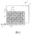
For example, in the superincumbent description, described wherein and alternately arranged photodiode 8 that is used in the time exposure and the example (see figure 3) that is used in the photodiode 8 in the short time exposure line by line and by row.Promptly, described the example that each row of photodiode 8 wherein comprises the identical photodiode that is used in time exposure 8 (or be used in the short time exposure photodiode 8), or wherein each row of photodiode 8 comprise the identical example that is used in photodiode 8 in the time exposure (or be used in the short time exposure photodiode 8).Yet scope of the present invention is not limited thereto, and as shown in figure 13, can alternately arrange photodiode 8 that is used in the time exposure and the photodiode 8 that is used in the short time exposure in each row or column of photodiode 8.
In the foregoing description, described the example that the row and column that wherein photodiode 8 is arranged in photodiode 8 is offset each other, but scope of the present invention is not limited thereto.For example, as shown in Figure 14 A to 14D, photodiode 8 can be arranged in the row and column of alignment light electric diode 8.
Figure 14 A to 14D is the example that the pixel of image-forming component of the imaging device of other embodiment is arranged.As shown in Figure 14 A, can alternately arrange photodiode 8 that is used in the time exposure and the photodiode 8 that is used in the short time exposure by every some row (for example by row).As shown in Figure 14B, can every several rows (for example line by line) alternately arrange photodiode 8 that is used in the time exposure and the photodiode 8 that is used in the short time exposure.
In addition, shown in Figure 14 C, photodiode 8 that is used in the time exposure and the photodiode 8 that is used in the short time exposure can alternately be arranged one by one, in the vertical and horizontal direction so that their form checkerboard pattern.As shown in Figure 14 D, can in the vertical and horizontal direction, alternately arrange photodiode 8 that is used in the time exposure and the photodiode 8 that is used in the short time exposure by block-by-block, so that they take advantage of the pieces of two row to form checkerboard patterns with two row.
Although described the content that is considered to the preferred embodiments of the present invention at present, will appreciate that, can make various improvement and modification to it, and accessory claim covers all these improvement and the modification that drops in practicalness of the present invention and the scope.
Industrial usability
As mentioned, imaging device of the present invention has advantage described below, that is, the time for exposure that can enlarge dynamic range and adjust each pixel groups according to the contrast between the bright and shade of object, and as will be for imaging device of surveillance camera etc. etc.
Claims (9)
1. imaging device comprises:
Image-generating unit, described image-generating unit can designated frame in the period pixel from each group of pixel groups read the accumulated charge signal of different exposure time, described pixel groups is time exposure pixel groups and short time exposure pixel groups, and all pixels are divided into described time exposure pixel groups and exposure of described short time pixel groups;
First reader is used for reading timing first after the time exposure period of described frame period and reads the accumulated charge signal of time exposure from described time exposure pixel groups;
Second reader is used for reading timing second after exposure period short time of described frame period and reads the accumulated charge signal of short time exposure from described short time exposure pixel groups;
Read regularly adjuster, be used for adjusting independently of one another described first and read regularly and described second read timing;
The time exposure signal generator is used to use the accumulated charge signal of the described time exposure of reading from described time exposure pixel groups and generates the time exposure signal;
Short time exposure signal maker is used to use the accumulated charge signal of the described short time exposure of reading from described short time exposure pixel groups and generates the short time exposure signal;
Synthesizer is used for synthetic described time exposure signal and described short time exposure signal, to generate the picture signal of representing all pixels; And
Third reading is got device, and be used for reading timing and read the accumulated charge signal of time exposure from described short time exposure pixel groups in described first of the described frame period,
Wherein, the accumulated charge signal that described time exposure signal generator adds the accumulated charge signal of the described time exposure of reading from described short time exposure pixel groups to read from described time exposure pixel groups described time exposure is to generate described time exposure signal.
2. imaging device as claimed in claim 1,
Wherein, described first reader comprises: first transfer path links to each other with each pixel in the described time exposure pixel groups; And the first grid electrode, described first grid electrode be each pixel from described time exposure pixel groups to the read path of described first transfer path,
Wherein, described second reader comprises: second transfer path links to each other with each pixel in described short time exposure pixel groups; And the second grid electrode, described second grid electrode be each pixel from described short time exposure pixel groups to the read path of described second transfer path, and
Wherein, the described adjuster that reads regularly reads regularly described first grid voltage is applied to described first grid electrode, and reads regularly described second grid voltage is applied to described second grid electrode.
3. imaging device as claimed in claim 1,
Wherein, described third reading is got device and comprised: first transfer path links to each other with each pixel in described short time exposure pixel groups; And the 3rd gate electrode, described the 3rd gate electrode be each pixel from described short time exposure pixel groups to the read path of described first transfer path, and
Wherein, the described adjuster that reads regularly reads regularly described first grid voltage is applied to described the 3rd gate electrode.
4. imaging device as claimed in claim 1 comprises:
The 4th reader is used for reading the accumulated charge signal that regularly reads the short time exposure from described time exposure pixel groups in second of the described frame period,
Wherein, the accumulated charge signal that described time exposure signal generator adds the accumulated charge signal of described short time exposure of reading from described time exposure pixel groups to read from described time exposure pixel groups described time exposure is to generate described time exposure signal.
5. imaging device as claimed in claim 4,
Wherein, described the 4th reader comprises: first transfer path links to each other with each pixel in the described time exposure pixel groups; And the first grid electrode, described first grid electrode be each pixel from described time exposure pixel groups to the read path of described first transfer path, and
Wherein, the described adjuster that reads regularly reads regularly described second grid voltage is applied to described first grid electrode.
6. as each described imaging device in the claim 1 to 5, wherein, in vertical or horizontal direction, alternately arrange pixel in the described time exposure pixel groups and the pixel in exposure of the described short time pixel groups.
7. as each described imaging device in the claim 1 to 5, wherein, described pixel is arranged in its pel array is the Baeyer array in each group of described time exposure pixel groups and exposure of described short time pixel groups.
8. imaging device as claimed in claim 6 wherein, is arranged in described pixel that its pel array is the Baeyer array in each group of described time exposure pixel groups and described short time exposure pixel groups.
9. formation method, wherein, use image-generating unit described below, promptly, described image-generating unit can designated frame in the period pixel from each group of pixel groups read the accumulated charge signal of different exposure time, described pixel groups is time exposure pixel groups and short time exposure pixel groups, and all pixels are divided into described time exposure pixel groups and exposure of described short time pixel groups
Described method comprises:
Adjust independently of one another that described frame first after time exposure period in the period reads regularly and described frame second after exposure period short time in the period read timing;
Read regularly described first, read the accumulated charge signal of time exposure from described time exposure pixel groups and exposure of described short time pixel groups respectively;
Read regularly described second, read the accumulated charge signal of short time exposure from described short time exposure pixel groups;
By the accumulated charge signal addition of the described time exposure of reading from described time exposure pixel groups and described short time exposure pixel groups is generated the time exposure signal;
The accumulated charge signal of the described short time exposure that use is read from described short time exposure pixel groups and generate the short time exposure signal; And
Synthetic described time exposure signal and described short time exposure signal are to generate the picture signal of representing all pixels.
Applications Claiming Priority (3)
| Application Number | Priority Date | Filing Date | Title |
|---|---|---|---|
| JP2006241243A JP5100066B2 (en) | 2006-09-06 | 2006-09-06 | Imaging apparatus and imaging method |
| JP241243/2006 | 2006-09-06 | ||
| PCT/JP2007/064972 WO2008029568A1 (en) | 2006-09-06 | 2007-07-31 | Imaging device, imaging method, and photographing program |
Publications (2)
| Publication Number | Publication Date |
|---|---|
| CN101507262A CN101507262A (en) | 2009-08-12 |
| CN101507262B true CN101507262B (en) | 2011-05-11 |
Family
ID=39157013
Family Applications (1)
| Application Number | Title | Priority Date | Filing Date |
|---|---|---|---|
| CN2007800311009A Expired - Fee Related CN101507262B (en) | 2006-09-06 | 2007-07-31 | Imaging device, imaging method |
Country Status (4)
| Country | Link |
|---|---|
| US (1) | US8264595B2 (en) |
| JP (1) | JP5100066B2 (en) |
| CN (1) | CN101507262B (en) |
| WO (1) | WO2008029568A1 (en) |
Families Citing this family (20)
| Publication number | Priority date | Publication date | Assignee | Title |
|---|---|---|---|---|
| JP4448888B2 (en) | 2008-04-01 | 2010-04-14 | 富士フイルム株式会社 | Imaging apparatus and signal processing method of imaging apparatus |
| JP4661922B2 (en) | 2008-09-03 | 2011-03-30 | ソニー株式会社 | Image processing apparatus, imaging apparatus, solid-state imaging device, image processing method, and program |
| JP2010279016A (en) * | 2009-04-30 | 2010-12-09 | Sony Corp | Solid-state imaging device, driving method thereof, and imaging apparatus |
| JP2011061684A (en) * | 2009-09-14 | 2011-03-24 | Fujifilm Corp | Solid-state imaging element and method of driving the same, and imaging device |
| JP5432799B2 (en) * | 2010-03-30 | 2014-03-05 | オリンパスイメージング株式会社 | Imaging apparatus, imaging system, and imaging method |
| WO2011132617A1 (en) * | 2010-04-20 | 2011-10-27 | 富士フイルム株式会社 | Imaging device and method of driving solid-state image sensor |
| CN102131051B (en) * | 2010-12-28 | 2012-11-28 | 惠州Tcl移动通信有限公司 | Image pick-up equipment and image acquisition method and device thereof |
| GB2497571A (en) | 2011-12-15 | 2013-06-19 | St Microelectronics Res & Dev | An imaging array with high dynamic range |
| WO2013129559A1 (en) | 2012-02-29 | 2013-09-06 | Etoh Takeharu | Solid-state imaging device |
| CN104322053B (en) * | 2012-05-25 | 2018-01-05 | 索尼半导体解决方案公司 | Imaging sensor, driving method and electronic installation |
| US9071765B2 (en) * | 2012-12-28 | 2015-06-30 | Nvidia Corporation | System, method, and computer program product implementing an image processing pipeline for high-dynamic range images |
| US9113097B2 (en) * | 2013-02-06 | 2015-08-18 | Canon Kabushiki Kaisha | Image capturing apparatus that controls performing of short-term and long-term exposures and corresponding read operations, and control method thereof |
| JP6172967B2 (en) * | 2013-02-20 | 2017-08-02 | キヤノン株式会社 | Imaging apparatus and control method thereof |
| JP5532171B2 (en) * | 2013-05-14 | 2014-06-25 | 株式会社Jvcケンウッド | Signal processing apparatus and signal processing method |
| TWI501639B (en) * | 2013-07-29 | 2015-09-21 | Quanta Comp Inc | Method of filming high dynamic range video |
| US9143708B2 (en) * | 2013-12-11 | 2015-09-22 | Himax Imaging, Inc. | Dual low voltage levels for control of transfer switch device in pixel array |
| KR102170627B1 (en) | 2014-01-08 | 2020-10-27 | 삼성전자주식회사 | Image sensor |
| JP6758946B2 (en) * | 2015-09-09 | 2020-09-23 | キヤノン株式会社 | Imaging device and playback device |
| JP6755780B2 (en) * | 2016-11-15 | 2020-09-16 | キヤノン株式会社 | Imaging device and imaging method |
| JP7086774B2 (en) * | 2018-07-25 | 2022-06-20 | キヤノン株式会社 | Imaging equipment, imaging methods and programs |
Citations (3)
| Publication number | Priority date | Publication date | Assignee | Title |
|---|---|---|---|---|
| CN1413411A (en) * | 1999-11-22 | 2003-04-23 | 松下电器产业株式会社 | Solid-state imaging device |
| CN1518724A (en) * | 2001-06-19 | 2004-08-04 | ������������ʽ���� | Image synthesizer |
| WO2006051936A3 (en) * | 2004-11-12 | 2007-01-04 | Matsushita Electric Ind Co Ltd | Imaging device |
Family Cites Families (11)
| Publication number | Priority date | Publication date | Assignee | Title |
|---|---|---|---|---|
| US3971065A (en) * | 1975-03-05 | 1976-07-20 | Eastman Kodak Company | Color imaging array |
| JPH08331461A (en) * | 1995-06-02 | 1996-12-13 | Sony Corp | Driving method for solid-state image pickup device |
| JPH09116815A (en) * | 1995-10-16 | 1997-05-02 | Sony Corp | Solid-state image pickup device |
| US6219097B1 (en) * | 1996-05-08 | 2001-04-17 | Olympus Optical Co., Ltd. | Image pickup with expanded dynamic range where the first exposure is adjustable and second exposure is predetermined |
| DE69841609D1 (en) * | 1997-10-17 | 2010-05-27 | Panasonic Corp | A video camera with extended dynamic range |
| JP2000092377A (en) * | 1998-09-11 | 2000-03-31 | Matsushita Electric Ind Co Ltd | Solid-state image pickup device |
| JP3674420B2 (en) * | 1999-11-22 | 2005-07-20 | 松下電器産業株式会社 | Solid-state imaging device |
| JP2001333331A (en) * | 2000-05-22 | 2001-11-30 | Hitachi Ltd | Image pickup device |
| JP2001352486A (en) * | 2000-06-07 | 2001-12-21 | Matsushita Electric Ind Co Ltd | Image pickup device |
| JP2004214363A (en) | 2002-12-27 | 2004-07-29 | Fuji Film Microdevices Co Ltd | Solid imaging device and digital camera |
| JP4131192B2 (en) * | 2003-04-25 | 2008-08-13 | コニカミノルタオプト株式会社 | Imaging apparatus, image processing apparatus, and image recording apparatus |
-
2006
- 2006-09-06 JP JP2006241243A patent/JP5100066B2/en not_active Expired - Fee Related
-
2007
- 2007-07-31 WO PCT/JP2007/064972 patent/WO2008029568A1/en active Application Filing
- 2007-07-31 CN CN2007800311009A patent/CN101507262B/en not_active Expired - Fee Related
- 2007-07-31 US US12/373,953 patent/US8264595B2/en not_active Expired - Fee Related
Patent Citations (3)
| Publication number | Priority date | Publication date | Assignee | Title |
|---|---|---|---|---|
| CN1413411A (en) * | 1999-11-22 | 2003-04-23 | 松下电器产业株式会社 | Solid-state imaging device |
| CN1518724A (en) * | 2001-06-19 | 2004-08-04 | ������������ʽ���� | Image synthesizer |
| WO2006051936A3 (en) * | 2004-11-12 | 2007-01-04 | Matsushita Electric Ind Co Ltd | Imaging device |
Non-Patent Citations (1)
| Title |
|---|
| JP平9-116815A 1997.05.02 |
Also Published As
| Publication number | Publication date |
|---|---|
| US20090262215A1 (en) | 2009-10-22 |
| US8264595B2 (en) | 2012-09-11 |
| WO2008029568A1 (en) | 2008-03-13 |
| JP2008066937A (en) | 2008-03-21 |
| CN101507262A (en) | 2009-08-12 |
| JP5100066B2 (en) | 2012-12-19 |
Similar Documents
| Publication | Publication Date | Title |
|---|---|---|
| CN101507262B (en) | Imaging device, imaging method | |
| US9942482B2 (en) | Image sensor with transfer gate control signal lines | |
| US10110827B2 (en) | Imaging apparatus, signal processing method, and program | |
| CN103125112B (en) | Imaging device and imaging method | |
| US8300131B2 (en) | Image pickup device for wide dynamic range at a high frame rate | |
| US7079184B2 (en) | Image pickup device with vertical and horizontal charge transfer devices operable in plural modes | |
| JP4448888B2 (en) | Imaging apparatus and signal processing method of imaging apparatus | |
| EP4160680A1 (en) | Image sensor with wide dynamic range | |
| US7218348B2 (en) | Solid-state electronic imaging device and method of controlling opertion thereof | |
| CN102859995B (en) | The method of imaging device and driving solid imaging element | |
| KR100605426B1 (en) | Solid state image pickup device and digital camera | |
| JP2009268078A (en) | Imaging element and imaging apparatus | |
| TW200425728A (en) | Solid-state imaging apparatus and its signal reading method | |
| US7655892B2 (en) | Solid-state imaging device, and method of driving solid-state imaging device | |
| CN102629994B (en) | Image sensing apparatus and image capture system | |
| CN101341735A (en) | Image sensor for still or video photography | |
| CN106506997A (en) | Imageing sensor including phase difference detection pixel | |
| JP2014217011A (en) | Solid state image sensor and imaging apparatus | |
| CN102948152A (en) | Imaging device and imaging method | |
| JP2006304248A (en) | Solid-state imaging element and drive method therefor | |
| JP2006246337A (en) | Solid-state imaging device and signal reading method thereof | |
| KR20150098547A (en) | Solid-state imaging apparatus and camera system | |
| KR20230113125A (en) | Image sensor and electronic device comprising thereof | |
| JPH0514597A (en) | Linear color image sensor |
Legal Events
| Date | Code | Title | Description |
|---|---|---|---|
| C06 | Publication | ||
| PB01 | Publication | ||
| C10 | Entry into substantive examination | ||
| SE01 | Entry into force of request for substantive examination | ||
| C14 | Grant of patent or utility model | ||
| GR01 | Patent grant | ||
| CF01 | Termination of patent right due to non-payment of annual fee |
Granted publication date: 20110511 Termination date: 20140731 |
|
| EXPY | Termination of patent right or utility model |