JP5079371B2 - Liquid crystal display device, test connector for liquid crystal display device, and test method thereof - Google Patents
Liquid crystal display device, test connector for liquid crystal display device, and test method thereof Download PDFInfo
- Publication number
- JP5079371B2 JP5079371B2 JP2007100532A JP2007100532A JP5079371B2 JP 5079371 B2 JP5079371 B2 JP 5079371B2 JP 2007100532 A JP2007100532 A JP 2007100532A JP 2007100532 A JP2007100532 A JP 2007100532A JP 5079371 B2 JP5079371 B2 JP 5079371B2
- Authority
- JP
- Japan
- Prior art keywords
- voltage
- gate
- liquid crystal
- pin
- crystal display
- Prior art date
- Legal status (The legal status is an assumption and is not a legal conclusion. Google has not performed a legal analysis and makes no representation as to the accuracy of the status listed.)
- Expired - Fee Related
Links
- 238000012360 testing method Methods 0.000 title claims description 104
- 239000004973 liquid crystal related substance Substances 0.000 title claims description 76
- 238000010998 test method Methods 0.000 title description 9
- 230000005540 biological transmission Effects 0.000 claims description 4
- 239000003990 capacitor Substances 0.000 description 18
- 238000010586 diagram Methods 0.000 description 15
- 230000007423 decrease Effects 0.000 description 6
- 238000007689 inspection Methods 0.000 description 6
- 238000000034 method Methods 0.000 description 3
- 238000007796 conventional method Methods 0.000 description 1
- 230000003247 decreasing effect Effects 0.000 description 1
- 230000002950 deficient Effects 0.000 description 1
- 230000009977 dual effect Effects 0.000 description 1
- 230000000694 effects Effects 0.000 description 1
- 238000004519 manufacturing process Methods 0.000 description 1
Images


Classifications
-
- G—PHYSICS
- G02—OPTICS
- G02F—OPTICAL DEVICES OR ARRANGEMENTS FOR THE CONTROL OF LIGHT BY MODIFICATION OF THE OPTICAL PROPERTIES OF THE MEDIA OF THE ELEMENTS INVOLVED THEREIN; NON-LINEAR OPTICS; FREQUENCY-CHANGING OF LIGHT; OPTICAL LOGIC ELEMENTS; OPTICAL ANALOGUE/DIGITAL CONVERTERS
- G02F1/00—Devices or arrangements for the control of the intensity, colour, phase, polarisation or direction of light arriving from an independent light source, e.g. switching, gating or modulating; Non-linear optics
- G02F1/01—Devices or arrangements for the control of the intensity, colour, phase, polarisation or direction of light arriving from an independent light source, e.g. switching, gating or modulating; Non-linear optics for the control of the intensity, phase, polarisation or colour
- G02F1/13—Devices or arrangements for the control of the intensity, colour, phase, polarisation or direction of light arriving from an independent light source, e.g. switching, gating or modulating; Non-linear optics for the control of the intensity, phase, polarisation or colour based on liquid crystals, e.g. single liquid crystal display cells
- G02F1/133—Constructional arrangements; Operation of liquid crystal cells; Circuit arrangements
-
- G—PHYSICS
- G09—EDUCATION; CRYPTOGRAPHY; DISPLAY; ADVERTISING; SEALS
- G09G—ARRANGEMENTS OR CIRCUITS FOR CONTROL OF INDICATING DEVICES USING STATIC MEANS TO PRESENT VARIABLE INFORMATION
- G09G3/00—Control arrangements or circuits, of interest only in connection with visual indicators other than cathode-ray tubes
- G09G3/006—Electronic inspection or testing of displays and display drivers, e.g. of LED or LCD displays
-
- G—PHYSICS
- G09—EDUCATION; CRYPTOGRAPHY; DISPLAY; ADVERTISING; SEALS
- G09G—ARRANGEMENTS OR CIRCUITS FOR CONTROL OF INDICATING DEVICES USING STATIC MEANS TO PRESENT VARIABLE INFORMATION
- G09G3/00—Control arrangements or circuits, of interest only in connection with visual indicators other than cathode-ray tubes
- G09G3/20—Control arrangements or circuits, of interest only in connection with visual indicators other than cathode-ray tubes for presentation of an assembly of a number of characters, e.g. a page, by composing the assembly by combination of individual elements arranged in a matrix no fixed position being assigned to or needed to be assigned to the individual characters or partial characters
- G09G3/34—Control arrangements or circuits, of interest only in connection with visual indicators other than cathode-ray tubes for presentation of an assembly of a number of characters, e.g. a page, by composing the assembly by combination of individual elements arranged in a matrix no fixed position being assigned to or needed to be assigned to the individual characters or partial characters by control of light from an independent source
- G09G3/36—Control arrangements or circuits, of interest only in connection with visual indicators other than cathode-ray tubes for presentation of an assembly of a number of characters, e.g. a page, by composing the assembly by combination of individual elements arranged in a matrix no fixed position being assigned to or needed to be assigned to the individual characters or partial characters by control of light from an independent source using liquid crystals
- G09G3/3611—Control of matrices with row and column drivers
- G09G3/3696—Generation of voltages supplied to electrode drivers
-
- G—PHYSICS
- G09—EDUCATION; CRYPTOGRAPHY; DISPLAY; ADVERTISING; SEALS
- G09G—ARRANGEMENTS OR CIRCUITS FOR CONTROL OF INDICATING DEVICES USING STATIC MEANS TO PRESENT VARIABLE INFORMATION
- G09G2330/00—Aspects of power supply; Aspects of display protection and defect management
- G09G2330/02—Details of power systems and of start or stop of display operation
-
- G—PHYSICS
- G09—EDUCATION; CRYPTOGRAPHY; DISPLAY; ADVERTISING; SEALS
- G09G—ARRANGEMENTS OR CIRCUITS FOR CONTROL OF INDICATING DEVICES USING STATIC MEANS TO PRESENT VARIABLE INFORMATION
- G09G3/00—Control arrangements or circuits, of interest only in connection with visual indicators other than cathode-ray tubes
- G09G3/20—Control arrangements or circuits, of interest only in connection with visual indicators other than cathode-ray tubes for presentation of an assembly of a number of characters, e.g. a page, by composing the assembly by combination of individual elements arranged in a matrix no fixed position being assigned to or needed to be assigned to the individual characters or partial characters
- G09G3/34—Control arrangements or circuits, of interest only in connection with visual indicators other than cathode-ray tubes for presentation of an assembly of a number of characters, e.g. a page, by composing the assembly by combination of individual elements arranged in a matrix no fixed position being assigned to or needed to be assigned to the individual characters or partial characters by control of light from an independent source
- G09G3/36—Control arrangements or circuits, of interest only in connection with visual indicators other than cathode-ray tubes for presentation of an assembly of a number of characters, e.g. a page, by composing the assembly by combination of individual elements arranged in a matrix no fixed position being assigned to or needed to be assigned to the individual characters or partial characters by control of light from an independent source using liquid crystals
- G09G3/3611—Control of matrices with row and column drivers
- G09G3/3648—Control of matrices with row and column drivers using an active matrix
-
- G—PHYSICS
- G09—EDUCATION; CRYPTOGRAPHY; DISPLAY; ADVERTISING; SEALS
- G09G—ARRANGEMENTS OR CIRCUITS FOR CONTROL OF INDICATING DEVICES USING STATIC MEANS TO PRESENT VARIABLE INFORMATION
- G09G5/00—Control arrangements or circuits for visual indicators common to cathode-ray tube indicators and other visual indicators
- G09G5/003—Details of a display terminal, the details relating to the control arrangement of the display terminal and to the interfaces thereto
- G09G5/006—Details of the interface to the display terminal
Landscapes
- Engineering & Computer Science (AREA)
- Physics & Mathematics (AREA)
- General Physics & Mathematics (AREA)
- Theoretical Computer Science (AREA)
- Computer Hardware Design (AREA)
- Crystallography & Structural Chemistry (AREA)
- Chemical & Material Sciences (AREA)
- Nonlinear Science (AREA)
- Mathematical Physics (AREA)
- Optics & Photonics (AREA)
- Control Of Indicators Other Than Cathode Ray Tubes (AREA)
- Liquid Crystal (AREA)
- Liquid Crystal Display Device Control (AREA)
Description
本発明は、タイミングコントローラおよびそれを含む液晶表示装置に関するものである。 The present invention relates to a timing controller and a liquid crystal display device including the timing controller.
液晶表示装置は、画素電極が備えられた第1表示板と、共通電極が備えられた第2表示板と、第1表示板と第2表示板との間に注入された誘電率異方性(dielectric anisotropy)を有する液晶層と、複数のゲートラインを駆動するゲート駆動部と、データ信号を出力するデータ駆動部と、基本階調電圧とゲートターンオンおよびターンオフ電圧を発生して出力する駆動装置とを含む。 A liquid crystal display device includes a first display panel having pixel electrodes, a second display panel having a common electrode, and a dielectric anisotropy injected between the first display panel and the second display panel. A liquid crystal layer having (dielectric anisotropy), a gate driver for driving a plurality of gate lines, a data driver for outputting a data signal, and a driver for generating and outputting a basic gradation voltage and gate turn-on and turn-off voltages Including.
このような液晶表示装置は、製造後、別途の検査装置を用いることによって不良であるか否かが判定される。このようなテストのうちの1つである高電圧ストレス(High Voltage Stress、以下「HVS」という)テストは、液晶表示装置に定格電圧レベルより高い電圧を印加して、液晶表示装置の動作をテストするテスト方法である。このようなHVSテストは、高電圧を供給する別途のHVS検査装置を備えて、HVSテスト装置と液晶表示装置とを電気的に接続して検査を行う。 Whether such a liquid crystal display device is defective or not is determined by using a separate inspection device after manufacture. A high voltage stress (hereinafter referred to as “HVS”) test, which is one of such tests, applies a voltage higher than the rated voltage level to the liquid crystal display device to test the operation of the liquid crystal display device. Test method to do. Such an HVS test includes a separate HVS inspection device that supplies a high voltage, and performs an inspection by electrically connecting the HVS test device and a liquid crystal display device.
このような従来技術によれば、高電圧を供給する別途のHVSテスト装置が必要となり、テスト過程も煩わしく、さらにHVSテスト装置は液晶表示装置の原価上昇の1つの要因にもなる。 According to such a conventional technique, a separate HVS test device for supplying a high voltage is required, and the test process is troublesome. Further, the HVS test device is one factor for increasing the cost of the liquid crystal display device.
本発明が達成しようとする技術的課題は、それ自体でHVSテストが可能な液晶表示装置を提供することにその目的がある。 The technical problem to be achieved by the present invention is to provide a liquid crystal display device capable of HVS testing by itself.
本発明が達成しようとする他の技術的課題は、それ自体でHVSテストが可能な液晶表示装置に用いられる液晶表示装置のテスト用コネクタを提供することにその目的がある。 Another technical problem to be achieved by the present invention is to provide a test connector for a liquid crystal display device used in a liquid crystal display device capable of performing an HVS test by itself.
本発明が達成しようとするまた他の技術的課題は、それ自体でHVSテストが可能な液晶表示装置のテスト方法を提供することにその目的がある。 Another technical problem to be achieved by the present invention is to provide a test method for a liquid crystal display device capable of performing an HVS test by itself.
本発明の技術的課題は、以上で言及した技術的課題に制限されず、言及していないまた他の技術的課題は下記記載によって当業者が明確に理解できるものである。 The technical problems of the present invention are not limited to the technical problems mentioned above, and other technical problems that are not mentioned can be clearly understood by those skilled in the art from the following description.
上記技術的課題を達成するための本発明の一態様に係る液晶表示装置は、外部から電源電圧が供給される入力ピンと、NC(No Connection)ピンと、グラウンドピンとを含む内部コネクタと、NCピンおよび入力ピンに接続された電源供給装置であって、電源電圧が供給されて、NCピンとグラウンドピンとの電気的接続の有無に応じて電圧レベルが調節されるゲートオン電圧およびゲートオフ電圧を出力する電源供給装置と、ゲートオン電圧およびゲートオフ電圧が供給されて、ゲート信号を供給するゲート駆動部と、ゲート信号を受信してオン/オフにし、映像を表示する複数の画素を含む液晶パネルとを含む。 In order to achieve the above technical problem, a liquid crystal display device according to an aspect of the present invention includes an input pin to which a power supply voltage is supplied from the outside, an internal connector including an NC (No Connection) pin, a ground pin, an NC pin, A power supply device connected to an input pin, wherein a power supply voltage is supplied and outputs a gate-on voltage and a gate-off voltage whose voltage level is adjusted according to the presence or absence of electrical connection between an NC pin and a ground pin And a gate driver for supplying a gate signal to which a gate-on voltage and a gate-off voltage are supplied, and a liquid crystal panel including a plurality of pixels that receive and turn on / off the gate signal and display an image.
他の技術的課題を達成するための本発明の他の態様に係る液晶表示装置のテスト用コネクタは、外部から供給される電源電圧と、グラウンド電圧と、テスト用映像信号とを受信して液晶表示装置に伝送する伝送部と、電源電圧と、グラウンド電圧と、テスト用映像信号とを受信する液晶表示装置の、内部コネクタのNCピンとグラウンドピンとを電気的に接続する接続部とを含む。 A test connector of a liquid crystal display device according to another aspect of the present invention for achieving another technical problem is a liquid crystal display which receives a power supply voltage, a ground voltage, and a test video signal supplied from the outside. A transmission unit that transmits to the display device, and a connection unit that electrically connects the NC pin and the ground pin of the internal connector of the liquid crystal display device that receives the power supply voltage, the ground voltage, and the test video signal.
他の技術的課題を達成するための本発明のまた他の態様に係る液晶表示装置のテスト方法は、外部から電源電圧が供給される入力ピンと、NC(No Connection)ピンと、グラウンドピンとを含む内部コネクタと、NCピンおよび入力ピンに接続された電源供給装置であって、電源電圧が供給されて、NCピンとグラウンドピンとの電気的接続の有無に応じて電圧レベルが調節されるゲートオン電圧およびゲートオフ電圧を出力する電源供給装置とを含む被テスト液晶表示装置を準備し、NCピンとグラウンドピンとを電気的に接続することを特徴とする。 According to another aspect of the present invention, there is provided a test method for a liquid crystal display device including an input pin to which a power supply voltage is supplied from the outside, an NC (No Connection) pin, and a ground pin. A power supply device connected to a connector, an NC pin, and an input pin, wherein a gate voltage and a gate-off voltage are adjusted according to the presence or absence of an electrical connection between the NC pin and the ground pin when a power voltage is supplied A liquid crystal display device to be tested including a power supply device that outputs a power supply is prepared, and an NC pin and a ground pin are electrically connected.
上述したような本発明に実施形態に係る液晶表示装置、液晶表示装置のテスト用コネクタ、およびそのテスト方法によれば次のような効果がある。 According to the liquid crystal display device, the test connector for the liquid crystal display device, and the test method thereof according to the embodiment of the present invention as described above, there are the following effects.
第1に、それ自体で液晶表示装置のHVSテストが可能である。第2に、液晶表示装置の検査過程がより簡単になる。第3に、高電圧を出力するHVS検査装置が不要になる。 First, the HVS test of the liquid crystal display device is possible by itself. Second, the inspection process of the liquid crystal display device becomes easier. Third, an HVS inspection device that outputs a high voltage is not necessary.
その他、実施形態の具体的な事項は、詳細な説明および図面に記載したとおりである。本発明の利点および特徴、そしてそれらを達成する方法は、添付する図面と共に詳細に後述する実施形態を参照すれば明確になる。しかし、本発明は以下にて開示する実施形態に限定されず、互いに異なる多様な形態によって実施され、単に本実施形態は本発明の開示が完全なものとなるようにし、本発明が属する技術分野で通常の知識を有する者に発明の範疇を完全に知らせるために提供されるものであって、本発明は請求項の記載に基づいてのみ定義されるものである。明細書の全体にわたり、同一参照符号は同一構成要素を示す。 In addition, the specific matter of embodiment is as having described in detailed description and drawing. Advantages and features of the present invention and methods for achieving them will be apparent with reference to the embodiments described below in detail with reference to the accompanying drawings. However, the present invention is not limited to the embodiments disclosed below, and can be implemented in various forms different from each other. The embodiments are merely intended to complete the disclosure of the present invention, and the technical field to which the present invention belongs. The present invention is provided only for those who have ordinary knowledge about the scope of the invention, and the present invention is defined only based on the description of the claims. Throughout the specification, the same reference numerals refer to the same components.
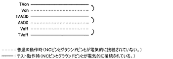
以下にて添付する図面を参照して、本発明の一実施形態に係る液晶表示装置およびそのテスト方法について説明する。図1は本発明の一実施形態に係る液晶表示装置およびそのテスト方法を説明するためのブロック図であり、図2は図1の1つの画素に対する等価回路図であり、図3は図1のコネクタの一例を示す図であり、図4は図1の電源供給装置を説明するためのグラフである。普通の動作時とテスト動作時に電源供給装置が供給する電圧を区分するために、テスト動作時に電源供給装置が供給する電圧は括弧の中に示す。 Hereinafter, a liquid crystal display device and a test method thereof according to an embodiment of the present invention will be described with reference to the accompanying drawings. FIG. 1 is a block diagram for explaining a liquid crystal display device and a test method thereof according to an embodiment of the present invention, FIG. 2 is an equivalent circuit diagram for one pixel of FIG. 1, and FIG. FIG. 4 is a diagram illustrating an example of a connector, and FIG. 4 is a graph for explaining the power supply device of FIG. 1. In order to distinguish the voltage supplied by the power supply device during the normal operation and the test operation, the voltage supplied by the power supply device during the test operation is shown in parentheses.
図1に示すように、本発明の一実施形態に係る液晶表示装置10は、液晶パネルアセンブリ300、ゲート駆動部400、データ駆動部500、信号制御部600、電源供給装置700、階調電圧発生部800、および内部コネクタ750を含む。
As shown in FIG. 1, a liquid
液晶パネルアセンブリ300は、等価回路で見る時、複数の表示信号線G1〜Gn,D1〜Dmと、それに接続されて行列状に配列された複数の画素PXとを含む。
When viewed in an equivalent circuit, the liquid
表示信号線G1〜Gn,D1〜Dmは、ゲート信号を伝送する複数のゲート線G1〜Gnと、データ信号を伝送する複数のデータ線D1〜Dmとを含む。ゲート線G1〜Gnは、大体行方向に延びて互いに略平行であり、データ線D1〜Dmは、大体列方向に延びて互いに略平行である。 The display signal lines G 1 to G n and D 1 to D m include a plurality of gate lines G 1 to G n that transmit gate signals and a plurality of data lines D 1 to D m that transmit data signals. The gate lines G 1 to G n extend in the row direction and are substantially parallel to each other, and the data lines D 1 to D m extend in the column direction and are substantially parallel to each other.
ここで、図2を参照すれば、液晶パネルアセンブリ300の1つの画素PXは、互いに対向する第1表示板100、第2表示板200、および両者の間に備えられた液晶層150を含む。第1表示板100の画素電極PEに対向するように第2表示板200の共通電極CEの一部領域に色フィルタCFが形成され得る。各画素、例えばi番目(i=1〜n)ゲート線Giとj番目(j=1〜m)データ線Djとに接続された画素は、信号線Gi,Djに接続された第1スイッチング素子Q1と、それに接続された液晶キャパシタClcおよびストレージキャパシタCstを含む。ストレージキャパシタCstは、場合によって省略され得る。
Here, referring to FIG. 2, one pixel PX of the liquid
内部コネクタ750は、外部のグラフィックコントローラ(図示せず)に接続されて、グラフィックコントローラ(図示せず)から供給される複数の信号を受信して液晶表示装置10の内部に伝送する。例えば、R,G,B映像信号R,G,B、およびこれらの表示を制御する入力制御信号を受信して信号制御部600に伝送する。入力制御信号の例としては、垂直同期信号Vsyncと垂直同期信号Hsync、メインクロックMCLK、データイネーブル信号DE等が挙げられる。また、外部から電源電圧Vddが供給されて電源供給装置700に供給する。内部コネクタ750は、上述したように電源電圧Vddおよび映像信号を受信して伝送する入力ピンと、グラウンド電圧が印加されるグラウンドピンと、ノーコネクション(No Connection、以下「NC」という)ピンとを含む。このような内部コネクタの例が図3に示されている。
The
図3に示すように、内部コネクタ750は、例えばPSWG(Panel Standardization Working Group)で標準化された30ピンのコネクタ750であってもよい。PSWGで標準化されたコネクタは、一般的に第1番ピンから第3番ピンまでは電源電圧VDDが入力されるピンであり、第4番ピン〜第6番ピンはNCピンNCであり、第7番ピン、第14番ピン、第17番ピン、第24番ピンはグラウンド電圧に接続されるグラウンドピンGNDであり、その他のピンは映像信号またはクロック信号が入力されるピンである。図面に示すRXOまたはRXEの「RX」は「Receiver」を意味する略字であり、「O」は「Odd」、「E」は「Even」の略字であって、帯域幅を向上することが可能なデュアル方式でデータを受信するためにピンをRXOとRXEに分けて割り当てられることを意味する。本発明では、コネクタのNCピンNCが電源供給装置700に接続される。
As shown in FIG. 3, the
一方、図1のゲート駆動部400は、信号制御部600からゲート制御信号CONT1を受信して、ゲート信号をゲート線G1〜Gnに印加する。ここで、ゲート信号は、普通の動作時には電源供給装置700から供給されるゲートオン電圧Vonとゲートオフ電圧Voffとの組み合わせからなる。テスト時にはテスト用ゲートオン電圧TVonとテスト用ゲートオフ電圧TVoffとの組み合わせからなる。ここで、テスト用ゲートオン電圧TVonは普通の動作時のゲートオン電圧Vonより電圧レベルが高く、テスト用ゲートオフ電圧TVoffは普通の動作時のゲートオフ電圧Voffより電圧レベルが低い。
On the other hand, the
ゲート制御信号CONT1は、ゲート駆動部400の動作を制御するための信号であって、ゲート駆動部400の動作を開始する垂直開始信号、ゲートオン電圧Vonの出力時期を決めるゲートクロック信号、およびゲートオン電圧Vonのパルス幅を決める出力イネーブル信号などを含むことができる。
The gate control signal CONT1 is a signal for controlling the operation of the
階調電圧発生部800は、普通の動作時には電源供給装置700から供給される駆動電圧AVDDを電圧分配して、複数の階調電圧GVをデータ駆動部500に供給し、テスト動作時にはテスト用駆動電圧TAVDDを電圧分解して、テスト用階調電圧TGVを供給する。
The
データ駆動部500は、信号制御部600からデータ制御信号CONT2を受信して動作し、階調電圧発生部800から供給される複数の階調電圧GVまたはテスト用階調電圧TGVのうちの映像信号に対応する映像データ電圧を選択して、データ線D1〜Dmに印加する。データ制御信号CONT2は、データ駆動部500の動作を制御する信号であって、データ駆動部500の動作を開始する水平開始信号、データ電圧の出力を指示する出力指示信号などを含む。
The
ゲート駆動部400またはデータ駆動部500は、複数の駆動集積回路チップの形態で液晶パネルアセンブリ300上に直接取り付けられたり、可撓性印刷回路フィルム(flexible printed circuit film)(図示せず)上に取り付けられたりして、テープキャリアパッケージ(tape carrier package)の形態で液晶パネル300に取り付けられ得る。その一方、ゲート駆動部400またはデータ駆動部500は、表示信号線G1〜Gn,D1〜Dmとスイッチング素子Q1などと共に液晶パネルアセンブリ300に集積されてもよい。
The
信号制御部600は、内部コネクタ750を介して伝送されるR,G,B映像信号およびこれらの表示を制御する入力制御信号を受信して、ゲート制御信号CONT1およびデータ制御信号CONT2を生成して、各々ゲート駆動部400およびデータ駆動部500に供給する。
The
電源供給装置700は、内部コネクタ750から電源電圧Vddが供給されて、液晶表示装置10の動作に必要な電圧を供給する。図3および図4を参照してより具体的に説明すれば、電源供給装置700は、普通の動作時には駆動電圧AVDD、ゲートオン電圧Von、およびゲートオフ電圧Voffを供給する。一方、テスト動作時には普通の動作時の駆動電圧AVDDおよびゲートオン電圧Vonより各々電圧レベルの高いテスト用駆動電圧TAVDDおよびテスト用ゲートオン電圧TVonを供給し、普通の動作時のゲートオフ電圧Voffより電圧レベルの低いテスト用ゲートオフ電圧TVoffを供給する。テスト動作時には内部コネクタ750のNCピンNCとグラウンドピンGNDとが電気的に接続され、普通の動作時には内部コネクタ750のNCピンNCとグラウンドピンGNDとが電気的に接続されない。すなわち、内部コネクタ750のNCピンNCとグラウンドピンGNDとが電気的に接続されるか否かに応じて、電源供給装置700は、駆動電圧AVDD、ゲートオン電圧Von、およびゲートオフ電圧Voffを供給し、あるいは駆動電圧AVDDおよびゲートオン電圧Vonより各々電圧レベルの高いテスト用駆動電圧TAVDDおよびテスト用ゲートオン電圧TVonを供給し、普通の動作時のゲートオフ電圧Voffより電圧レベルの低いテスト用ゲートオフ電圧TVoffを供給する。これに関する詳細な説明は以下のとおりである。
The
図5は図1の電源供給装置を説明するためのブロック図であり、図6は図5のブースト部とフィードバック電圧生成部を説明するための回路図であり、図7は図5のPWM信号発生器を説明するためのブロック図であり、図8は図5のゲートオン電圧生成部およびゲートオフ電圧生成部を説明するための回路図である。 5 is a block diagram for explaining the power supply device of FIG. 1, FIG. 6 is a circuit diagram for explaining the boost unit and the feedback voltage generation unit of FIG. 5, and FIG. 7 is a PWM signal of FIG. FIG. 8 is a block diagram for explaining a generator, and FIG. 8 is a circuit diagram for explaining a gate-on voltage generator and a gate-off voltage generator of FIG.
図5に示すように、電源供給装置700は、ブースト部720、ゲートオン電圧生成部730、ゲートオフ電圧生成部740、およびフィードバック電圧生成部710を含む。
As shown in FIG. 5, the
内部コネクタ750の電源電圧ピンVddはブースト部720に接続され、NCピンNCはフィードバック電圧生成部710に接続され、グラウンドピンGNDはゲートオフ電圧生成部740に接続される。
The power supply voltage pin Vdd of the
先ず、ブースト部720は電源電圧Vddをブーストして、フィードバック電圧FBの電圧レベルに応じて電圧レベルが可変する駆動電圧AVDDおよびパルス信号PULSEを出力する。例えば、フィードバック電圧FBの電圧レベルが減少すれば、駆動電圧AVDDおよびパルス信号PULSEの電圧レベルは上昇し、フィードバック電圧FBの電圧レベルが上昇すれば、駆動電圧AVDDおよびパルス信号PULSEの電圧レベルは減少する。内部コネクタ750のNCピンNCとグラウンドピンGNDとが電気的に接続されると、フィードバック電圧生成部710はフィードバック電圧FBの電圧レベルを減少させる。すなわち、NCピンNCとグラウンドピンGNDとが電気的に接続されると、フィードバック電圧生成部710は、NCピンNCとグラウンドピンGNDとが電気的に接続されない場合より低いレベルのフィードバック電圧FBをブースト部720に供給し、ブースト部720は、普通の動作時の駆動電圧AVDDおよびパルス信号PULSEより高いレベルのテスト用駆動電圧TAVDDと、パルス信号PULSEとを出力する。このようなブースト部720およびフィードバック電圧生成部710については、図6および図7を参照して後述する。
First, the
ゲートオン電圧生成部730は、普通の動作時には駆動電圧AVDDをパルス信号PULSEの電圧レベルだけシフトしてゲートオン電圧Vonを出力し、テスト動作時には、すなわちNCピンNCとグラウンドピンGNDとが電気的に接続されると、テスト用ゲートオン電圧TVonを出力する。このようなゲートオン電圧生成部730については図8を参照して後述する。
The gate-on
ゲートオフ電圧生成部740は、普通の動作時にはグラウンド電圧GNDをパルス信号PULSEの電圧レベルだけシフトしてゲートオフ電圧Voffを出力し、テスト動作時には、すなわちNCピンNCとグラウンドピンGNDとが電気的に接続されると、テスト用ゲートオフ電圧TVoffを出力する。このようなゲートオフ電圧生成部740については図8を参照して後述する。
The gate-off
図6を参照して、ブースト部720とフィードバック電圧生成部710についてより詳細に説明する。先ず、フィードバック電圧生成部710を説明すれば、フィードバック電圧生成部710は、駆動電圧AVDDを電圧分配する第1抵抗R1および第2抵抗R2と、オプション抵抗R_OPとを含む。第1抵抗R1は駆動電圧AVDDとフィードバック電圧FBとの間に接続され、第2抵抗R2はフィードバック電圧FBとグラウンド電圧との間に接続される。オプション抵抗R_OPの一端はフィードバック電圧FBに接続され、他端は内部コネクタ750のNCピンNCに接続される。
The
NCピンNCとグラウンドピンGNDとが電気的に接続されなければ、オプション抵抗R_OPはフローティング状態になり、フィードバック電圧FBは、駆動電圧AVDDが第1抵抗R1と第2抵抗R2によって電圧分配された電圧レベルになる。すなわち、NCピンNCとグラウンドピンGNDとが電気的に接続されなければ、普通の動作としてブースト部720は駆動電圧AVDDを出力する。
If the NC pin NC and the ground pin GND are not electrically connected, the option resistor R_OP is in a floating state, and the feedback voltage FB is a voltage obtained by dividing the drive voltage AVDD by the first resistor R1 and the second resistor R2. Become a level. That is, if the NC pin NC and the ground pin GND are not electrically connected, the
テスト時には、NCピンNCとグラウンドピンGNDとが電気的に接続され、オプション抵抗R_OPの他端はグラウンド電圧に接続されて、第2抵抗R2と並列に接続される。したがって、フィードバック電圧FBとグラウンド電圧との間の抵抗値は減少して、フィードバック電圧FBの電圧レベルは減少する。フィードバック電圧FBレベルが減少すれば、ブースト部720は、普通の動作時の駆動電圧AVDDおよびパルス信号PULSEより高いレベルのテスト用駆動電圧TAVDDおよびパルス信号PULSEを出力する。したがって、電源供給装置は、高い電圧レベルのテスト用駆動電圧TAVDD、テスト用ゲートオン電圧Von、およびテスト用ゲートオフ電圧Voffを供給するようになる。ここで、NCピンNCとグラウンドピンGNDとは、伝導性の接続部材CM、例えばケーブルなどによって電気的に接続されてもよい。
During the test, the NC pin NC and the ground pin GND are electrically connected, and the other end of the option resistor R_OP is connected to the ground voltage and connected in parallel with the second resistor R2. Therefore, the resistance value between the feedback voltage FB and the ground voltage decreases, and the voltage level of the feedback voltage FB decreases. When the feedback voltage FB level decreases, the
ブースト部720は、図6に示すように、ブーストコンバータであって、内部コネクタ750から供給された電源電圧Vddが印加されるインダクタLと、インダクタLにアノードが接続され、駆動電圧AVDDにカソードが接続される第1ダイオードD1と、第1ダイオードD1と接地との間に接続される第1キャパシタC1と、第1ダイオードD1のアノード端子に接続されるPWM(Pulse Width Modulation)信号発生器725とを含む。ここで、ブーストコンバータは、ブースト部720の一例であって、他種のコンバーターであり得る。ただし、図6に示すものとは異なり、電圧分圧器(ディバイダ、図示せず)を介して電源電圧Vddより低い電圧がブースト部720に供給されてもよい。
As shown in FIG. 6, the
動作について説明すれば、PWM信号発生器725から出力されたPWM信号PWMがハイレベルである場合にスイッチング素子Q2がターンオンし、インダクタLの電流、電圧特性に応じてインダクタLの両端に印加される電源電圧Vddに比例して、インダクタLを流れる電流ILが徐々に増加する。
In terms of operation, when the PWM signal PWM output from the
PWM信号PWMがローレベルであれば、スイッチング素子Q2がターンオフし、インダクタLを流れる電流ILは第1ダイオードD1を介して流れて、第1キャパシタC1の電流、電圧特性に応じて第1キャパシタC1に電圧が充電される。したがって、電源電圧Vddが一定電圧に昇圧して、電源供給装置700に出力される。ここで、PWM信号PWMは、フィードバック電圧FBの電圧レベルに応じてデューティ比(duty ratio)が変わるが、PWM信号PWMのデューティー比によってインダクタLに流れる電流の量が変わるようになり、これに伴って駆動電圧AVDDおよびパルス信号PULSEが昇圧したりあるいは降圧したりする。
If the PWM signal PWM is at a low level, the switching element Q2 is turned off, the current I L flowing through the inductor L flows through the first diode D1, a current of the first capacitor C1, a first capacitor in response to the voltage characteristic C1 is charged with voltage. Therefore, the power supply voltage Vdd is boosted to a constant voltage and output to the
図7を参照してPWM信号発生器725がフィードバック電圧FBの電圧レベルに応じてデューティ比が可変するPWM信号PWMを出力する動作について説明すれば、オシレータ726は一定の周波数の基準クロック信号RCLKを発生する。比較器727は、オシレータ726から生成された基準クロック信号RCLKとフィードバック電圧FBとを比較して、フィードバック電圧FBのレベルが基準クロック信号RCLKのレベルより大きい場合はハイレベルを出力し、小さい場合はローレベルを出力して、PWM信号PWMを生成する。ここで基準クロック信号RCLKの周波数は一定であるため、フィードバック電圧FBのレベルに応じてPWM信号PWMのデューティ比が変わる。ただし、PWM信号発生器725はこれに限定されず、フィードバック電圧FBに応じてデューティ比が変わるPWM信号PWMを発生する他種の回路であってもよい。
Referring to FIG. 7, the operation of the
すなわち、ブースト部720は、NCピンNCとグラウンドピンGNDとが電気的に接続されると、普通の動作時より電圧レベルの高いパルス信号PULSEとテスト用駆動電圧TAVDDとを出力する。
That is, when the NC pin NC and the ground pin GND are electrically connected, the
図8を参照して、ゲートオン電圧生成部730およびゲートオフ電圧生成部740がチャージポンプ回路である場合を例に挙げて説明する。
With reference to FIG. 8, the case where gate-on
ゲートオン電圧生成部730は、第2および第3ダイオードD2,D3と第2および第3キャパシタC2,C3とを含む。第2ダイオードD2のアノードに普通の動作時の駆動電圧またはテスト用駆動電圧TAVDDが供給され、第2ダイオードD2のカソードは第1ノードN1に接続される。第2キャパシタC2は、第1ノードN1とパルス信号PULSEが印加される第2ノードN2との間に接続される。第3ダイオードD3のアノードは第1ノードN1に接続され、第3ダイオードD3のカソードは普通の動作時のゲートオン電圧Vonまたはテスト用ゲートオン電圧TVonを出力する。第3キャパシタC3は、第2ダイオードD2のアノードと第3ダイオードD3のカソードとの間に接続される。ただし、これに限定されず、3つ以上のダイオードと3つ以上のキャパシタとの組み合わせであってもよい。
The gate-on
動作について説明すれば、パルス信号PULSEが第2キャパシタC2に供給されると、第1ノードN1は、普通の動作時には駆動電圧AVDDからパルス信号PULSEの電圧レベルだけ上昇したパルスを出力し、テスト動作時にはテスト用駆動電圧TAVDDからパルス信号PULSEの電圧レベルだけ上昇したパルスを出力する。第3ダイオードD3および第3キャパシタC3は、第1ノードN1の電圧をクランプして、ゲートオン電圧Vonまたはテスト用ゲートオン電圧TVonを出力する。すなわち、普通の動作時のゲートオン電圧Vonは駆動電圧AVDDが略パルス信号PULSEの電圧レベルだけシフトしたDC電圧になり、テスト用ゲートオン電圧TVonはテスト用駆動電圧TAVDDが略パルス信号PULSEの電圧レベルだけシフトしたDC電圧になる。 In operation, when the pulse signal PULSE is supplied to the second capacitor C2, the first node N1 outputs a pulse that is increased from the drive voltage AVDD by the voltage level of the pulse signal PULSE during a normal operation, and performs a test operation. Sometimes, a pulse that is raised from the test drive voltage TAVDD by the voltage level of the pulse signal PULSE is output. The third diode D3 and the third capacitor C3 clamp the voltage of the first node N1, and output the gate-on voltage Von or the test gate-on voltage TVon. That is, the gate-on voltage Von during normal operation is a DC voltage in which the drive voltage AVDD is shifted by approximately the voltage level of the pulse signal PULSE, and the test gate-on voltage TVon is the test drive voltage TAVDD being approximately the voltage level of the pulse signal PULSE. The shifted DC voltage is obtained.
ゲートオフ電圧生成部740は、第4および第5ダイオードD4,D5と第4および第5キャパシタC4,C5とを含む。第4ダイオードD4のカソードにグラウンド電圧が供給され、第4ダイオードD4のアノードは第3ノードN3に接続される。第4キャパシタC4は、第3ノードN3とパルス信号PULSEが印加される第2ノードN2との間に接続される。第5ダイオードD5のカソードは第3ノードN3に接続され、第5ダイオードD5のアノードはゲートオフ電圧Voffまたはテスト用ゲートオフ電圧TVoffを出力する。第5キャパシタC5は、第4ダイオードD4のカソードと第5ダイオードD5のアノードとの間に接続される。ただし、ここに限定されす、3つ以上のダイオードと3つ以上のキャパシタの組み合わせであってもよい。
The gate-off
動作について説明すれば、パルス信号PULSEが第4キャパシタC4に供給されると、第3ノードN3はグラウンド電圧からパルス信号PULSEの電圧レベルだけ下降したパルスを出力する。ここでパルス信号PULSEの電圧レベルは、上述したように、NCピンNCとグラウンドピンGNDとが電気的に接続されると、接続されない場合より上昇する。第5ダイオードN5および第5キャパシタC5は、第3ノードN3の電圧をクランプして、ゲートオフ電圧Voffまたはテスト用ゲートオフ電圧TVoffを出力する。すなわち、ゲートオフ電圧Voffまたはテスト用ゲートオフ電圧TVoffは、略グラウンド電圧がパルス信号PULSEの電圧レベルだけシフトしたDC電圧になる。 In operation, when the pulse signal PULSE is supplied to the fourth capacitor C4, the third node N3 outputs a pulse that is lowered from the ground voltage by the voltage level of the pulse signal PULSE. Here, as described above, when the NC pin NC and the ground pin GND are electrically connected, the voltage level of the pulse signal PULSE rises more than the case where they are not connected. The fifth diode N5 and the fifth capacitor C5 clamp the voltage of the third node N3 and output the gate-off voltage Voff or the test gate-off voltage TVoff. That is, the gate-off voltage Voff or the test gate-off voltage TVoff is a DC voltage in which the ground voltage is substantially shifted by the voltage level of the pulse signal PULSE.
つまり、NCピンNCとグラウンドピンGNDとが電気的に接続されると、電源供給装置(図1の700)がテスト用駆動電圧TAVDD、テスト用ゲートオン電圧TVon、およびテスト用ゲートオフ電圧TVoffを供給する。すなわち、高電圧をそれ自体で生成するため、別途の液晶表示装置のHVS検査装置が不要になる。 That is, when the NC pin NC and the ground pin GND are electrically connected, the power supply device (700 in FIG. 1) supplies the test drive voltage TAVDD, the test gate-on voltage TVon, and the test gate-off voltage TVoff. . That is, since a high voltage is generated by itself, a separate HVS inspection device for a liquid crystal display device is not required.
図9を参照して、本発明の一実施形態に係る液晶表示装置のテスト用コネクタについて説明する。図9は、本発明の一実施形態に係る液晶表示装置のテスト用コネクタを説明するための液晶表示装置のテストシステムのブロック図である。図1に示す構成要素と同じ機能を有する構成要素に対しては同一の図面符号を用い、説明の便宜上、該当構成要素に関する詳細説明は省略する。 With reference to FIG. 9, a test connector for a liquid crystal display device according to an embodiment of the present invention will be described. FIG. 9 is a block diagram of a test system for a liquid crystal display device for explaining a test connector for the liquid crystal display device according to an embodiment of the present invention. Components having the same functions as those shown in FIG. 1 are denoted by the same reference numerals, and detailed description of the corresponding components is omitted for convenience of explanation.
図9に示すように、テストシステムは、テスト用信号R,G,B,DE,Hsync,Vsync,MCLKを供給する外部信号供給装置900と、外部信号供給装置900からテスト用信号R,G,B,DE,Hsync,Vsync,MCLKを液晶表示装置10に伝送する液晶表示装置のテスト用コネクタ760、および被テスト液晶表示装置10を含む。
As shown in FIG. 9, the test system includes an external
液晶表示装置10をテストするために、テスト用コネクタ760が液晶表示装置10の内部コネクタ750に接続され、テスト用コネクタ760が外部信号供給装置900に接続される。
In order to test the liquid
外部信号供給装置900は、テスト用映像信号R,G,Bと制御信号DE,Hsync,Vsync,MCLK、および電源電圧Vddおよびグラウンド電圧GNDを供給する。ここで、テスト用映像信号R,G,Bは液晶表示装置10の表示品質をテストするためにパターン化した信号であってもよい。
The external
テスト用コネクタ760は伝送部762,764と接続部766とを含む。伝送部762,764は、外部信号供給装置900からテスト用信号R,G,B,DE,Hsync,Vsync,MCLKが入力される入力端子762と、これらを液晶表示装置10に伝送する出力端子764とを含む。接続部766は、液晶表示装置の内部コネクタ750のNCピンNCに接続される第1接続端子P1とグラウンドピンGNDに接続される第2接続端子P2とを含む。ここで、第1接続端子P1と第2接続端子P2とは電気的に接続されている。このようなテスト用コネクタ760は、テスト用信号R,G,B,DE,Hsync,Vsync,MCLKを液晶表示装置10の内部コネクタ750に供給する。また、テスト用コネクタ760は、外部信号供給装置900から電源電圧Vddと、グラウンド電圧GNDとが供給されて内部コネクタ750に供給することもでき、他の装置から供給され得るため、外部からの電源電圧Vddとグラウンド電圧GNDの入力は具体的に示していない。
The
内部コネクタ750がテスト用コネクタ760に接続されると、NCピンNCとグラウンドピンGNDとが電気的に接続されるため、電源供給装置700は、上述したように、テスト用駆動電圧TAVDD、テスト用ゲートオン電圧TVon、およびテスト用ゲートオフ電圧TVoffを供給する。
When the
信号制御部600はテスト用映像信号DATをデータ駆動部500に供給し、データ駆動部500はテスト用階調電圧TGのうちのテスト用映像信号DATに対応する映像データ電圧を液晶パネル300に供給する。
The
つまり、テスト用コネクタ760によって、液晶表示装置10内部の電源供給装置700がそのもので高電圧のテスト用駆動電圧TAVDD、テスト用ゲートオン電圧TVon、およびテスト用ゲートオフ電圧TVoffを生成し、このようなテスト用電圧TAVDD,TVon,TVoffと、テスト用コネクタ760を介して外部から供給されるテスト用映像信号R,G,Bとを用いて液晶表示装置10をテストすることができる。
That is, the
以上、添付した図面を参照して本発明の実施形態を説明したが、本発明が属する技術分野で通常の知識を有する者であれば、本発明がその技術的思想や必須の特徴を変更せず、他の具体的な形態によって実施することができるということを理解できる。したがって、以上で記述した実施形態はすべての面で例示的なものであり、限定的なものではないことを理解しなければならない。 The embodiments of the present invention have been described above with reference to the accompanying drawings. However, the present invention may be modified by those who have ordinary knowledge in the technical field to which the present invention belongs. However, it can be understood that the present invention can be implemented in other specific forms. Therefore, it should be understood that the embodiments described above are illustrative in all aspects and not limiting.
本発明は、液晶表示装置、液晶表示装置のテスト用コネクタ、およびそのテスト方法に用いることができる。 The present invention can be used in a liquid crystal display device, a test connector for a liquid crystal display device, and a test method thereof.
10 液晶表示装置
300 液晶パネル
400 ゲート駆動部
500 データ駆動部
600 信号制御部
700 電源供給装置
710 フィードバック電圧生成部
720 ブースト部
730 ゲートオン電圧生成部
740 ゲートオフ電圧生成部
750 内部コネクタ
760 テスト用コネクタ
800 階調電圧発生部
900 外部信号供給装置
NC NCピン
GND グラウンドピン
DESCRIPTION OF
Claims (5)
前記内部コネクタから電源電圧が供給されて液晶表示装置の動作に必要な駆動電圧を供給する電源供給装置とを含む液晶表示装置であって、
前記電源供給装置は、ブースト部とフィードバック電圧生成部とゲートオン電圧生成部とゲートオフ電圧生成部とを含み、
前記フィードバック電圧生成部は、前記ブースト部から出力される前記駆動電圧を電圧分配する第1抵抗および第2抵抗と、オプション抵抗とを含み、
前記第1抵抗の一端は前記駆動電圧を伝達する配線に接続され、前記第1抵抗の他端はフィードバック電圧を伝達する配線に接続され、前記第2抵抗の一端は前記フィードバック電圧を伝達する配線に接続され、前記第2抵抗の他端はグランドに接続され、前記オプション抵抗の一端は前記フィードバック電圧を伝達する配線に接続され、前記オプション抵抗の他端は前記NCピンに接続され、
前記NCピンと前記グラウンドピンとが電気的に接続されると、前記フィードバック電圧は第1レベルのフィードバック電圧となり、
前記NCピンと前記グラウンドピンとが電気的に絶縁されると、前記フィードバック電圧は第2レベルのフィードバック電圧となり、
前記ブースト部は、前記フィードバック電圧生成部より第1レベルのフィードバック電圧が入力されると第1レベルパルス信号を生成し、前記ゲートオン電圧生成部および前記ゲートオフ電圧生成部に供給し、前記第2レベルのフィードバック電圧が入力されると前記第1レベルパルス信号とは異なる電圧レベルの第2レベルパルス信号を前記ゲートオン電圧生成部および前記ゲートオフ電圧生成部に供給し、
前記ゲートオン電圧生成部および前記ゲートオフ電圧生成部は、前記第1レベルパルス信号または前記第2レベルパルス信号のいずれかが入力されると、入力されたパルス信号に応じて電圧の大きさが異なるゲートオン電圧またはゲートオフ電圧を生成する
ことを特徴とする液晶表示装置。 An internal connector including an external video signal input pin, a clock signal input pin, an input pin to which a power supply voltage is supplied, an NC (No Connection) pin, and a ground pin to which a ground voltage is applied ;
A power supply device that is supplied with a power supply voltage from the internal connector and supplies a driving voltage necessary for the operation of the liquid crystal display device,
The power supply device includes a boost unit, a feedback voltage generation unit, a gate-on voltage generation unit, and a gate-off voltage generation unit,
The feedback voltage generation unit includes a first resistor and a second resistor for voltage distribution of the drive voltage output from the boost unit, and an optional resistor,
One end of the first resistor is connected to a wiring that transmits the driving voltage, the other end of the first resistor is connected to a wiring that transmits a feedback voltage, and one end of the second resistor is a wiring that transmits the feedback voltage. The other end of the second resistor is connected to the ground, one end of the optional resistor is connected to a wiring that transmits the feedback voltage, and the other end of the optional resistor is connected to the NC pin,
When the NC pin and the ground pin are electrically connected, the feedback voltage becomes a first level feedback voltage,
When the NC pin and the ground pin are electrically isolated, the feedback voltage becomes a second level feedback voltage,
The boost unit generates a first level pulse signal when a first level feedback voltage is input from the feedback voltage generation unit, and supplies the first level pulse signal to the gate-on voltage generation unit and the gate-off voltage generation unit. When the feedback voltage is input, a second level pulse signal having a voltage level different from that of the first level pulse signal is supplied to the gate-on voltage generation unit and the gate-off voltage generation unit,
When the first level pulse signal or the second level pulse signal is input, the gate-on voltage generation unit and the gate-off voltage generation unit have different voltage magnitudes according to the input pulse signal. Generate voltage or gate-off voltage
The liquid crystal display device, characterized in that.
前記ゲートオン電圧生成部は前記第1レベルパルス信号が入力されると前記第2レベルパルス信号が入力される場合よりも高いゲートオン電圧を生成し、
前記ゲートオフ電圧生成部は前記第1レベルパルス信号が入力されると前記第2レベルパルス信号が入力される場合よりも低いゲートオフ電圧を生成する
ことを特徴とする請求項1、2および3のいずれかに記載の液晶表示装置。 The first level feedback voltage is lower than the second level feedback voltage;
The gate-on voltage generator generates a high gate-on voltage than the case where the second-level pulse signal and the first level pulse signal is input is input,
The gate-off voltage generator generates a lower gate-off voltage than the case where the first level pulse signal is the second level pulse signal to be input is input
The liquid crystal display device according to claim 1, wherein the liquid crystal display device is a liquid crystal display device.
ブースト部とフィードバック電圧生成部とゲートオン電圧生成部とゲートオフ電圧生成部とを含む電源供給装置を含む液晶表示装置とからなる液晶表示装置のテストシステムであって、
前記フィードバック電圧生成部は、前記ブースト部から出力される前記駆動電圧を電圧分配する第1抵抗および第2抵抗と、オプション抵抗とを含み、
前記第1抵抗の一端は前記駆動電圧を伝達する配線に接続され、前記第1抵抗の他端はフィードバック電圧を伝達する配線に接続され、前記第2抵抗の一端は前記フィードバック電圧を伝達する配線に接続され、前記第2抵抗の他端はグランドに接続され、前記オプション抵抗の一端は前記フィードバック電圧を伝達する配線に接続され、前記オプション抵抗の他端は前記NCピンに接続され、
前記NCピンと前記グラウンドピンとが電気的に接続されると、前記フィードバック電圧は第1レベルのフィードバック電圧となり、
前記NCピンと前記グラウンドピンとが電気的に絶縁されると、前記フィードバック電圧は第2レベルのフィードバック電圧となり、
前記ブースト部は、前記フィードバック電圧生成部より第1レベルのフィードバック電圧が入力されると第1レベルパルス信号を生成し、前記ゲートオン電圧生成部および前記ゲートオフ電圧生成部に供給し、前記第2レベルのフィードバック電圧が入力されると前記第1レベルパルス信号とは異なる電圧レベルの第2レベルパルス信号を前記ゲートオン電圧生成部および前記ゲートオフ電圧生成部に供給し、
前記ゲートオン電圧生成部および前記ゲートオフ電圧生成部は、前記第1レベルパルス信号または前記第2レベルパルス信号のいずれかが入力されると、入力されたパルス信号に応じて電圧の大きさが異なるゲートオン電圧またはゲートオフ電圧を生成する
ことを特徴とする液晶表示装置のテストシステム。 A transmission unit that receives an externally supplied power supply voltage, a ground voltage, and a test video signal and transmits the test video signal to the liquid crystal display device; and the power supply voltage, the ground voltage, and the test video signal that are received A test connector for a liquid crystal display device including a connection portion for electrically connecting the NC pin and the ground pin of the internal connector of the liquid crystal display device;
A test system for a liquid crystal display device comprising a liquid crystal display device including a power supply device including a boost unit, a feedback voltage generation unit, a gate-on voltage generation unit, and a gate-off voltage generation unit,
The feedback voltage generation unit includes a first resistor and a second resistor for voltage distribution of the drive voltage output from the boost unit, and an optional resistor,
One end of the first resistor is connected to a wiring that transmits the driving voltage, the other end of the first resistor is connected to a wiring that transmits a feedback voltage, and one end of the second resistor is a wiring that transmits the feedback voltage. The other end of the second resistor is connected to the ground, one end of the optional resistor is connected to a wiring that transmits the feedback voltage, and the other end of the optional resistor is connected to the NC pin,
When the NC pin and the ground pin are electrically connected, the feedback voltage becomes a first level feedback voltage,
When the NC pin and the ground pin are electrically isolated, the feedback voltage becomes a second level feedback voltage,
The boost unit generates a first level pulse signal when a first level feedback voltage is input from the feedback voltage generation unit, and supplies the first level pulse signal to the gate-on voltage generation unit and the gate-off voltage generation unit. When the feedback voltage is input, a second level pulse signal having a voltage level different from that of the first level pulse signal is supplied to the gate-on voltage generation unit and the gate-off voltage generation unit,
When the first level pulse signal or the second level pulse signal is input, the gate-on voltage generation unit and the gate-off voltage generation unit have different voltage magnitudes according to the input pulse signal. Generate voltage or gate-off voltage
Test system of the liquid crystal display device, characterized in that.
Applications Claiming Priority (2)
| Application Number | Priority Date | Filing Date | Title |
|---|---|---|---|
| KR1020060133053A KR100843148B1 (en) | 2006-12-22 | 2006-12-22 | Liquid crystal display, connector for testing liquid crystal display and test method thereof |
| KR10-2006-0133053 | 2006-12-22 |
Publications (3)
| Publication Number | Publication Date |
|---|---|
| JP2008158480A JP2008158480A (en) | 2008-07-10 |
| JP2008158480A5 JP2008158480A5 (en) | 2010-05-20 |
| JP5079371B2 true JP5079371B2 (en) | 2012-11-21 |
Family
ID=39542061
Family Applications (1)
| Application Number | Title | Priority Date | Filing Date |
|---|---|---|---|
| JP2007100532A Expired - Fee Related JP5079371B2 (en) | 2006-12-22 | 2007-04-06 | Liquid crystal display device, test connector for liquid crystal display device, and test method thereof |
Country Status (4)
| Country | Link |
|---|---|
| US (1) | US7911217B2 (en) |
| JP (1) | JP5079371B2 (en) |
| KR (1) | KR100843148B1 (en) |
| CN (1) | CN101206323B (en) |
Families Citing this family (28)
| Publication number | Priority date | Publication date | Assignee | Title |
|---|---|---|---|---|
| CN101086508B (en) * | 2006-06-07 | 2010-05-12 | 瀚斯宝丽股份有限公司 | Checking apparatus and its connector and checking method |
| CN101424795B (en) * | 2007-11-02 | 2010-12-01 | 群康科技(深圳)有限公司 | LCD and detecting method thereof |
| KR101427592B1 (en) * | 2007-12-21 | 2014-08-08 | 삼성디스플레이 주식회사 | Inspecting apparatus for liquid crystal display and control method thereof |
| KR101492116B1 (en) | 2008-01-24 | 2015-02-09 | 삼성디스플레이 주식회사 | A connector and display device havine the same |
| JP5428299B2 (en) * | 2008-03-18 | 2014-02-26 | セイコーエプソン株式会社 | Electro-optical device and electronic apparatus |
| US20090267877A1 (en) * | 2008-04-29 | 2009-10-29 | Himax Display, Inc. | Liquid crystal on silicon panel |
| TWI379116B (en) * | 2008-05-30 | 2012-12-11 | Chimei Innolux Corp | Liquid crystal display high-voltage testing circuit and method of testing liquid crystal display |
| TWI395041B (en) * | 2008-07-16 | 2013-05-01 | Electronic paper display screen pin device | |
| KR101485584B1 (en) * | 2008-08-06 | 2015-01-28 | 삼성디스플레이 주식회사 | Liquid crystal display device and method for operating the same |
| CN101719352B (en) | 2008-10-09 | 2012-07-25 | 北京京东方光电科技有限公司 | Device and method for detection after forming liquid crystal box |
| CN102187400A (en) * | 2008-10-20 | 2011-09-14 | 国立大学法人东京大学 | Integrated circuit device |
| CN101958091B (en) * | 2009-07-15 | 2012-10-31 | 北京京东方光电科技有限公司 | Post-casing detection device and method for liquid crystal display panel |
| CN102063877B (en) * | 2009-11-12 | 2013-01-02 | 群康科技(深圳)有限公司 | LCD (Liquid Crystal Display) and detecting method thereof |
| JP2013058428A (en) * | 2011-09-09 | 2013-03-28 | Japan Display East Co Ltd | Connector connection checking circuit, display, method for checking connector connection, and method for manufacturing display |
| US20130273776A1 (en) * | 2012-04-16 | 2013-10-17 | Shenzhen China Star Optoelectronics Technology Co Ltd. | Conversion Adaptor and LCD Inspection System |
| US8994219B2 (en) * | 2012-12-25 | 2015-03-31 | Shenzhen China Star Optoelectronics Technology Co., Ltd | DC/DC module of LCD driving circuit |
| CN104732913B (en) * | 2013-12-19 | 2018-12-14 | 昆山国显光电有限公司 | The screen body structure and its voltage conversion circuit of AMOLED |
| KR102374748B1 (en) * | 2015-06-30 | 2022-03-17 | 엘지디스플레이 주식회사 | Power supply and display device using the same |
| CN105161065B (en) * | 2015-09-30 | 2017-10-27 | 深圳市华星光电技术有限公司 | Liquid crystal display signal control circuit, display panel and display device |
| KR102618361B1 (en) * | 2017-02-02 | 2023-12-27 | 삼성디스플레이 주식회사 | Display device |
| CN107038985B (en) | 2017-06-02 | 2020-04-03 | 京东方科技集团股份有限公司 | Driving module for display panel, display panel and display device |
| CN107316618B (en) * | 2017-07-19 | 2019-11-12 | 深圳市华星光电半导体显示技术有限公司 | DC voltage conversion circuit and DC voltage conversion method and liquid crystal display device |
| CN107329291A (en) * | 2017-08-11 | 2017-11-07 | 深圳同兴达科技股份有限公司 | A kind of liquid crystal display module efficient detection system |
| CN108615490B (en) * | 2018-03-16 | 2022-03-01 | 昆山龙腾光电股份有限公司 | Test circuit |
| CN112368762A (en) * | 2018-06-29 | 2021-02-12 | 堺显示器制品株式会社 | Display device |
| CN113160728B (en) * | 2021-02-19 | 2024-02-20 | 厦门天马微电子有限公司 | Display panel, high-voltage omission detection method for detecting display panel and display device |
| CN113745865B (en) * | 2021-08-30 | 2022-09-09 | 武汉华星光电技术有限公司 | Pin connector and display panel |
| CN113920957B (en) * | 2021-10-29 | 2022-07-26 | 重庆惠科金渝光电科技有限公司 | Liquid crystal display device and driving method thereof |
Family Cites Families (20)
| Publication number | Priority date | Publication date | Assignee | Title |
|---|---|---|---|---|
| JPH08202320A (en) * | 1995-01-25 | 1996-08-09 | Nec Home Electron Ltd | Mode changeover method and device for display device |
| JP4147594B2 (en) * | 1997-01-29 | 2008-09-10 | セイコーエプソン株式会社 | Active matrix substrate, liquid crystal display device, and electronic device |
| KR100239749B1 (en) * | 1997-04-11 | 2000-01-15 | 윤종용 | Tft fabrication method structure of lcd, test apparatus and method for gross test |
| JP3206509B2 (en) * | 1997-08-22 | 2001-09-10 | 日本電気株式会社 | Probe device for display panel |
| JPH11186516A (en) | 1997-12-17 | 1999-07-09 | Toshiba Microelectronics Corp | Semiconductor memory device and method for testing the same |
| KR100365943B1 (en) * | 1999-04-08 | 2002-12-26 | 주식회사 하이닉스반도체 | A high voltage generating device for a burn in test using internal voltage |
| JP2001272430A (en) * | 2000-03-24 | 2001-10-05 | Oht Inc | Apparatus and method for inspection |
| JP2002156417A (en) * | 2000-11-17 | 2002-05-31 | Oht Inc | Apparatus and method for inspecting circuit board |
| KR100758809B1 (en) * | 2000-12-30 | 2007-09-13 | 엘지.필립스 엘시디 주식회사 | Apparatus Of Inspfcting Liquid Crystal Display |
| JP2002340989A (en) * | 2001-05-15 | 2002-11-27 | Semiconductor Energy Lab Co Ltd | Measuring method, inspection method and inspection apparatus |
| US6940271B2 (en) * | 2001-08-17 | 2005-09-06 | Nptest, Inc. | Pin electronics interface circuit |
| JP4685336B2 (en) * | 2003-06-06 | 2011-05-18 | 株式会社島津製作所 | TFT array inspection equipment |
| KR20060015201A (en) * | 2004-08-13 | 2006-02-16 | 삼성전자주식회사 | Array substrate and mother board and liquid crystal display having the same |
| CN100359556C (en) * | 2004-09-13 | 2008-01-02 | 凌阳科技股份有限公司 | Source driver of built-in detecting circuit and its detecting method |
| KR101209050B1 (en) * | 2005-02-22 | 2012-12-06 | 삼성디스플레이 주식회사 | Liquid crystal display and test method thereof |
| KR101172498B1 (en) * | 2005-06-01 | 2012-08-10 | 삼성전자주식회사 | Method for manufacturing liquid crystal display apparatus, liquid crystal display apparatus and aging system |
| KR20060131021A (en) | 2005-06-14 | 2006-12-20 | 삼성전자주식회사 | Display device |
| KR101147120B1 (en) * | 2005-08-30 | 2012-05-25 | 엘지디스플레이 주식회사 | Apparatus for Testing LCD Panel |
| JP2007072285A (en) * | 2005-09-08 | 2007-03-22 | Funai Electric Co Ltd | Liquid crystal display device and inspecting device for liquid crystal cell |
| JP5019194B2 (en) * | 2005-11-30 | 2012-09-05 | 株式会社ジャパンディスプレイセントラル | Display control circuit |
-
2006
- 2006-12-22 KR KR1020060133053A patent/KR100843148B1/en not_active IP Right Cessation
-
2007
- 2007-04-06 JP JP2007100532A patent/JP5079371B2/en not_active Expired - Fee Related
- 2007-09-05 US US11/850,415 patent/US7911217B2/en active Active
- 2007-10-16 CN CN2007101802762A patent/CN101206323B/en not_active Expired - Fee Related
Also Published As
| Publication number | Publication date |
|---|---|
| KR100843148B1 (en) | 2008-07-02 |
| KR20080058872A (en) | 2008-06-26 |
| US20080150856A1 (en) | 2008-06-26 |
| CN101206323B (en) | 2011-06-15 |
| US7911217B2 (en) | 2011-03-22 |
| CN101206323A (en) | 2008-06-25 |
| JP2008158480A (en) | 2008-07-10 |
Similar Documents
| Publication | Publication Date | Title |
|---|---|---|
| JP5079371B2 (en) | Liquid crystal display device, test connector for liquid crystal display device, and test method thereof | |
| CN109889040B (en) | DC-DC converter | |
| KR101330216B1 (en) | Liquid crystal display | |
| US9384701B2 (en) | Backlight driver with luminance control and liquid crystal display including the same | |
| US8363004B2 (en) | Method of driving a light source, light source device for performing the same, and display device having the light source device | |
| US8624524B2 (en) | Power management and control module and liquid crystal display device | |
| CN105551414B (en) | Display device and its driving method | |
| KR101485584B1 (en) | Liquid crystal display device and method for operating the same | |
| US8928701B2 (en) | Display apparatus and method of driving the same | |
| KR101369398B1 (en) | Liquid crystal display and driving method thereof | |
| CN105528981A (en) | Display device and power control device | |
| US20100295876A1 (en) | Display apparatus | |
| JP2007011346A (en) | Display device and drive apparatus for the display device | |
| US8248399B2 (en) | Driving-voltage generation apparatus and liquid crystal display having the same | |
| CN115527483A (en) | Pixel circuit, control method thereof and display device | |
| KR20090009395A (en) | Driving device and display device including the same | |
| KR102654549B1 (en) | Data Driving Device For Determining Faulty Bonding And Display Device Including The Same | |
| KR20140079044A (en) | Power supply and flat panel display using the same | |
| KR101979010B1 (en) | Backlight driver and liquid crystal display device including the same | |
| KR20110075414A (en) | Liquid crystal display device and method of driving the same | |
| KR20240042935A (en) | Power management circuit and display device | |
| KR20140098367A (en) | Power supply and flat panel display using the same | |
| KR20070079181A (en) | Test voltage generator and test system of liquid crystal display apparatus | |
| US20240013736A1 (en) | Power supply system for display apparatus | |
| KR20070077923A (en) | Driver and liquid crystal display apparatus comprising the same |
Legal Events
| Date | Code | Title | Description |
|---|---|---|---|
| A521 | Request for written amendment filed |
Free format text: JAPANESE INTERMEDIATE CODE: A523 Effective date: 20100401 |
|
| A621 | Written request for application examination |
Free format text: JAPANESE INTERMEDIATE CODE: A621 Effective date: 20100401 |
|
| A521 | Request for written amendment filed |
Free format text: JAPANESE INTERMEDIATE CODE: A523 Effective date: 20110301 |
|
| A131 | Notification of reasons for refusal |
Free format text: JAPANESE INTERMEDIATE CODE: A131 Effective date: 20120403 |
|
| A521 | Request for written amendment filed |
Free format text: JAPANESE INTERMEDIATE CODE: A523 Effective date: 20120703 |
|
| TRDD | Decision of grant or rejection written | ||
| A01 | Written decision to grant a patent or to grant a registration (utility model) |
Free format text: JAPANESE INTERMEDIATE CODE: A01 Effective date: 20120731 |
|
| A01 | Written decision to grant a patent or to grant a registration (utility model) |
Free format text: JAPANESE INTERMEDIATE CODE: A01 |
|
| A61 | First payment of annual fees (during grant procedure) |
Free format text: JAPANESE INTERMEDIATE CODE: A61 Effective date: 20120829 |
|
| FPAY | Renewal fee payment (event date is renewal date of database) |
Free format text: PAYMENT UNTIL: 20150907 Year of fee payment: 3 |
|
| R150 | Certificate of patent or registration of utility model |
Free format text: JAPANESE INTERMEDIATE CODE: R150 |
|
| FPAY | Renewal fee payment (event date is renewal date of database) |
Free format text: PAYMENT UNTIL: 20150907 Year of fee payment: 3 |
|
| S111 | Request for change of ownership or part of ownership |
Free format text: JAPANESE INTERMEDIATE CODE: R313111 |
|
| S631 | Written request for registration of reclamation of domicile |
Free format text: JAPANESE INTERMEDIATE CODE: R313631 |
|
| FPAY | Renewal fee payment (event date is renewal date of database) |
Free format text: PAYMENT UNTIL: 20150907 Year of fee payment: 3 |
|
| R371 | Transfer withdrawn |
Free format text: JAPANESE INTERMEDIATE CODE: R371 |
|
| S111 | Request for change of ownership or part of ownership |
Free format text: JAPANESE INTERMEDIATE CODE: R313111 |
|
| S631 | Written request for registration of reclamation of domicile |
Free format text: JAPANESE INTERMEDIATE CODE: R313631 |
|
| R350 | Written notification of registration of transfer |
Free format text: JAPANESE INTERMEDIATE CODE: R350 |
|
| R250 | Receipt of annual fees |
Free format text: JAPANESE INTERMEDIATE CODE: R250 |
|
| R250 | Receipt of annual fees |
Free format text: JAPANESE INTERMEDIATE CODE: R250 |
|
| LAPS | Cancellation because of no payment of annual fees |