JP5073760B2 - Galvanic isolated charging balance system - Google Patents
Galvanic isolated charging balance system Download PDFInfo
- Publication number
- JP5073760B2 JP5073760B2 JP2009547284A JP2009547284A JP5073760B2 JP 5073760 B2 JP5073760 B2 JP 5073760B2 JP 2009547284 A JP2009547284 A JP 2009547284A JP 2009547284 A JP2009547284 A JP 2009547284A JP 5073760 B2 JP5073760 B2 JP 5073760B2
- Authority
- JP
- Japan
- Prior art keywords
- cell
- variable conductance
- galvanic
- flying capacitor
- bias circuit
- Prior art date
- Legal status (The legal status is an assumption and is not a legal conclusion. Google has not performed a legal analysis and makes no representation as to the accuracy of the status listed.)
- Expired - Fee Related
Links
Images
Classifications
-
- H—ELECTRICITY
- H02—GENERATION; CONVERSION OR DISTRIBUTION OF ELECTRIC POWER
- H02J—ELECTRIC POWER NETWORKS; CIRCUIT ARRANGEMENTS OR SYSTEMS FOR SUPPLYING OR DISTRIBUTING ELECTRIC POWER; SYSTEMS FOR STORING ELECTRIC ENERGY
- H02J7/00—Circuit arrangements for charging or discharging batteries or for supplying loads from batteries
- H02J7/50—Circuit arrangements for charging or discharging batteries or for supplying loads from batteries acting upon multiple batteries simultaneously or sequentially
- H02J7/52—Circuit arrangements for charging or discharging batteries or for supplying loads from batteries acting upon multiple batteries simultaneously or sequentially for charge balancing, e.g. equalisation of charge between batteries
- H02J7/54—Passive balancing, e.g. using resistors or parallel MOSFETs
-
- H—ELECTRICITY
- H02—GENERATION; CONVERSION OR DISTRIBUTION OF ELECTRIC POWER
- H02J—ELECTRIC POWER NETWORKS; CIRCUIT ARRANGEMENTS OR SYSTEMS FOR SUPPLYING OR DISTRIBUTING ELECTRIC POWER; SYSTEMS FOR STORING ELECTRIC ENERGY
- H02J7/00—Circuit arrangements for charging or discharging batteries or for supplying loads from batteries
- H02J7/50—Circuit arrangements for charging or discharging batteries or for supplying loads from batteries acting upon multiple batteries simultaneously or sequentially
- H02J7/52—Circuit arrangements for charging or discharging batteries or for supplying loads from batteries acting upon multiple batteries simultaneously or sequentially for charge balancing, e.g. equalisation of charge between batteries
-
- H—ELECTRICITY
- H02—GENERATION; CONVERSION OR DISTRIBUTION OF ELECTRIC POWER
- H02J—ELECTRIC POWER NETWORKS; CIRCUIT ARRANGEMENTS OR SYSTEMS FOR SUPPLYING OR DISTRIBUTING ELECTRIC POWER; SYSTEMS FOR STORING ELECTRIC ENERGY
- H02J7/00—Circuit arrangements for charging or discharging batteries or for supplying loads from batteries
- H02J7/80—Circuit arrangements for charging or discharging batteries or for supplying loads from batteries including monitoring or indicating arrangements
- H02J7/82—Control of state of charge [SOC]
Landscapes
- Engineering & Computer Science (AREA)
- Power Engineering (AREA)
- Charge And Discharge Circuits For Batteries Or The Like (AREA)
- Secondary Cells (AREA)
Description
本発明は、ガルバニック絶縁充電平衡システムに関する。 The present invention relates to a galvanic isolated charge balancing system.
バッテリーを長持ちさせるための一手法に、複数のセルのすべてを平衡させるようにバッテリーの1つ以上のセルを放電する(受動的)充電平衡化回路がある。典型的に、これは、各セルからの漏れ電流を個々に制御することによってなされる。例えば、トランジスタスイッチ及び直列抵抗器が、各セルと並列に配置される。スイッチは、関連するセルの過充電に応じて、所定時間だけターンオンする。例えば、過充電が大きいほど、スイッチは放電を持続するように長時間保持される。このことに対する欠点の1つが、マルチセルバッテリーにおいて、ただ1つのセル又は少数のセルが充電不足となった場合に、複数のセルのうちの多数側を少数の充電不足のセルの充電レベルへと下げるように放電するという非効率性である。別の(能動的)手法は、充電を行うことであり、例えば、フライングコンデンサを介して、充電不足の1つ又は少数のセルに充電を行って、それらを他のセルの充電レベルへと上昇させる。これには、充電不足となった複数のセルに選択的に充電を行うために、複雑なスイッチ行列が必要となる。 One approach to making the battery last is a (passive) charge balancing circuit that discharges one or more cells of the battery to balance all of the cells. Typically this is done by individually controlling the leakage current from each cell. For example, transistor switches and series resistors are arranged in parallel with each cell. The switch is turned on for a predetermined time in response to overcharging of the associated cell. For example, the greater the overcharge, the longer the switch is held to sustain the discharge. One drawback to this is that in a multi-cell battery, if only one cell or a small number of cells are undercharged, the majority of the cells are reduced to the charge level of a small number of undercharged cells. Inefficiency of discharging. Another (active) approach is to charge, for example via a flying capacitor, charge one or a few of the undercharged cells and raise them to the charge level of the other cells Let This requires a complicated switch matrix in order to selectively charge a plurality of cells that have become insufficiently charged.
したがって、この発明の目的は、改良されたガルバニック絶縁充電平衡システムを提供することにある。 Accordingly, it is an object of the present invention to provide an improved galvanic isolated charge balancing system.
この発明のさらなる目的は、充電平衡化のためにオン−オフ及び/又は線形制御を用いることが可能な、上記の改良されたガルバニック絶縁充電平衡システムを提供することにある。 It is a further object of the present invention to provide an improved galvanically isolated charge balancing system as described above that can use on-off and / or linear control for charge balancing.
本発明は、改良された、能動的又は受動的に動作する(充電又は放電を行う)マルチセルバッテリー用ガルバニック絶縁充電平衡システムが、ガルバニック絶縁MEMSスイッチを用いて実現されることによって成る。MEMSスイッチは、フライングコンデンサを電圧供給源とバイアス回路とに選択的に接続する。電圧供給源に接続された場合には、関連するセルが所定の電圧に充電される。バイアス回路に接続された場合には、関連するセルの充電状態を所定のレベルに調整するように、可変コンダクタンススイッチが設定される。 The present invention consists of an improved active or passively operating (charging or discharging) galvanically isolated charge balancing system for a multi-cell battery implemented using galvanically isolated MEMS switches. The MEMS switch selectively connects the flying capacitor to the voltage supply source and the bias circuit. When connected to a voltage supply, the associated cell is charged to a predetermined voltage. When connected to the bias circuit, the variable conductance switch is set to adjust the state of charge of the associated cell to a predetermined level.
しかしながら、発明の要旨は、他の実施形態において、それらすべての目的を達成する必要はなく、特許請求の範囲は、それらの目的を達成可能な構成又は方法に限定されるべきではない。 However, the gist of the invention need not achieve all of these objectives in other embodiments, and the scope of the claims should not be limited to configurations or methods capable of achieving those objectives.
この発明は、バッテリーの各セルに関連した平衡化回路を具備するガルバニック絶縁充電平衡システムを特徴とする。各平衡化回路は、フライングコンデンサと、可変コンダクタンススイッチとを具備する。また、可変コンダクタンススイッチのためのバイアス回路と、ガルバニック絶縁MEMSスイッチングデバイスとがある。MEMSスイッチングデバイスは、フライングコンデンサを電圧供給源とバイアス回路とに選択的に接続する。電圧供給源に接続された場合、フライングコンデンサは所定の電圧に充電される。バイアス回路に接続された場合、関連するセルの充電状態を所定のレベルに調整するように、可変コンダクタンススイッチを設定する。 The invention features a galvanically isolated charge balancing system that includes a balancing circuit associated with each cell of the battery. Each balancing circuit includes a flying capacitor and a variable conductance switch. There are also bias circuits for variable conductance switches and galvanically isolated MEMS switching devices. The MEMS switching device selectively connects the flying capacitor to the voltage supply and the bias circuit. When connected to a voltage supply source, the flying capacitor is charged to a predetermined voltage. When connected to a bias circuit, the variable conductance switch is set to adjust the state of charge of the associated cell to a predetermined level.
好適な実施形態において、可変コンダクタンススイッチは、トランジスタであってよい。トランジスタは、MOSFETであってよい。バイアス回路は、コンデンサであってよい。所定の電圧は、セルを所定のレベルに放電するために、可変コンダクタンススイッチを設定してよい。所定の電圧は、セルを充電するために、又は充電されるセルが所定のレベルとなるように、可変コンダクタンススイッチを設定してもよい。所定の電圧は、外部電流供給源の電流レベルのうちの所定の割合である電流レベルでセルを所定のレベルに充電するように、可変コンダクタンススイッチを設定してもよい。 In a preferred embodiment, the variable conductance switch may be a transistor. The transistor may be a MOSFET. The bias circuit may be a capacitor. The predetermined voltage may set a variable conductance switch to discharge the cell to a predetermined level. The predetermined voltage may set the variable conductance switch to charge the cell or so that the charged cell is at a predetermined level. The variable conductance switch may be set to charge the cell to a predetermined level at a current level that is a predetermined ratio of the current level of the external current supply source.
また、本発明は、マルチセルバッテリーの各セルに関連した平衡化回路を具備するガルバニック絶縁充電平衡システムを特徴とする。各平衡化回路は、フライングコンデンサと、可変コンダクタンススイッチと、該可変コンダクタンススイッチのためのバイアス回路とを具備する。ガルバニック絶縁MEMSスイッチングデバイスは、フライングコンデンサを電圧供給源とバイアス回路とに選択的に接続する。電圧供給源に接続された場合、フライングコンデンサは所定の電圧に充電される。バイアス回路に接続された場合、関連するセルを所定のレベルに放電するように、可変コンダクタンススイッチが設定される。 The invention also features a galvanically isolated charge balancing system comprising a balancing circuit associated with each cell of the multi-cell battery. Each balancing circuit includes a flying capacitor, a variable conductance switch, and a bias circuit for the variable conductance switch. A galvanic isolation MEMS switching device selectively connects a flying capacitor to a voltage supply and a bias circuit. When connected to a voltage supply source, the flying capacitor is charged to a predetermined voltage. When connected to a bias circuit, the variable conductance switch is set to discharge the associated cell to a predetermined level.
また、本発明は、マルチセルバッテリーの各セルに関連した平衡化回路を具備するガルバニック絶縁充電平衡システムを特徴とする。各平衡化回路は、フライングコンデンサと、可変コンダクタンススイッチと、該可変コンダクタンススイッチのためのバイアス回路とを具備する。ガルバニック絶縁MEMSスイッチングデバイスは、フライングコンデンサを電圧供給源とバイアス回路とに選択的に接続する。電圧供給源に接続された場合、フライングコンデンサは所定の電圧に充電される。バイアス回路に接続された場合、関連するセルを所定のレベルに充電するように、可変コンダクタンススイッチが設定される。 The invention also features a galvanically isolated charge balancing system comprising a balancing circuit associated with each cell of the multi-cell battery. Each balancing circuit includes a flying capacitor, a variable conductance switch, and a bias circuit for the variable conductance switch. A galvanic isolation MEMS switching device selectively connects a flying capacitor to a voltage supply and a bias circuit. When connected to a voltage supply source, the flying capacitor is charged to a predetermined voltage. When connected to a bias circuit, the variable conductance switch is set to charge the associated cell to a predetermined level.
その他の目的、特徴、及び利点は、好適な実施形態の以下の記載と添付の図面とから、当業者に明らかとなる。 Other objects, features and advantages will become apparent to those skilled in the art from the following description of the preferred embodiment and the accompanying drawings.
好適な実施形態又は以下に記載の実施形態のほかにも、この発明は、他の複数の実施形態となってよく、かつさまざまな方法で実施又は実行されてよい。故に、当然のことながら、本発明は、その出願において、以下に記載された又は図面に示された詳細な構造及び要素の構成に限定されない。明細書中に1つの実施形態しか記載されていなかったとしても、特許請求の範囲は、その実施形態に限定されない。さらに、特許請求の範囲は、ある除外、制限、又は限定修正を表す明白かつ納得のできる根拠がある場合を除き、限定的に解釈されない。 In addition to the preferred embodiments or the embodiments described below, the present invention may be other embodiments and may be implemented or carried out in various ways. Thus, it should be understood that the present invention is not limited in that application to the detailed structure and arrangement of elements set forth below or shown in the drawings. Even if only one embodiment is described in the specification, the claims are not limited to that embodiment. Further, the claims are not to be construed as limiting unless there is a clear and convincing basis for some exclusion, limitation, or modification.
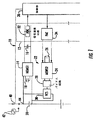
図1には、ガルバニック絶縁信号調整システム10が示されている。信号調整システム10は、信号調整回路12と、フライングコンデンサ18及びホールドコンデンサ16と並んだMEMSデバイス14とを具備し、図示されていない多数のバッテリーセルのうちの1つのバッテリーセル20に対して機能する。また、図1には、この発明によるガルバニック絶縁充電平衡システム22が示されている。充電平衡システム22は、MEMSデバイス24と、フライングコンデンサ26と、バイアス回路28と、可変コンダクタンススイッチ30とを具備する。図1には、1つの信号調整システム10及び1つの充電平衡システム22と一緒に、1つのセル20だけしか示されていないが、典型的に、多数のセルは、自身に関連したこの発明によるガルバニック絶縁信号調整システム及びガルバニック絶縁充電平衡システムをそれぞれ具備する。信号調整回路は、特に、アナログ−デジタル変換部32と、デジタル−アナログ変換部34とを具備し、また、制御部36として示される。
FIG. 1 shows a galvanic isolation
動作中、MEMS14は、バッテリーセル20からのセル電圧に代表されるような所定の電圧に、フライングコンデンサ18を充電し、次いで、フライングコンデンサ18を切り換えて、ホールドコンデンサ16を充電する。次いで、ホールドコンデンサ16上の電圧は、ADC 32と、信号調整回路12を介して参照符号36で示されたような制御部とに供給される。各セルはホールドコンデンサ16に電圧を印加するために使用されるが、制御部36は、そのセルの充電量を判断するために、ADC 32を監視する。このようにして、制御部36は、複数のバッテリーセルのそれぞれの電圧を監視するとともに、それぞれの充電状態を判断する。複数のバッテリーセルのすべての充電状態を平衡化するために、制御部36は、予め選択された充電レベル未満のセルに充電を行うように能動的に動作するか、又は、予め選択されたレベルを超えたバッテリーセルを消耗(ドレイン)又は放電するように能動モードで動作するかのいずれかを行うことができる。
During operation, the
この発明によるガルバニック絶縁充電平衡システム22は、どちらの場合にも適用できる。例えば、制御部36は、受動モードで動作しており、かつ全バッテリーセルは、バッテリーセル20のそれよりも低い所定のレベルにあるとする。したがって、バッテリーセル20は、そのより低い予め選択されたレベルに放電される。この場合、制御部36は、フライングコンデンサ26に所定の電圧を与えるように、DAC 34に命令する。フライングコンデンサ26は、バイアス回路28に作用するMEMSデバイス24によって切り換えられたとき、可変コンダクタンススイッチ30に、セル20を所定のレベルに減少させるためにセル20から過不足なく充電量が消耗するようにさせる。好適な実施形態によれば、可変コンダクタンススイッチ30は、リニアスイッチである。すなわち、可変コンダクタンススイッチ30は、オン及びオフ状態だけではなく、オンとオフとの間のさまざまな導通レベルを有する。実際には、所定のレベル以上となる多数のセルが存在することがあり、それらは、予め選択されたレベルを超えた異なるレベルとなる。フライングコンデンサ26に適用される必要とされる調整及び要求された所定の合成電圧は、設計事項であって、制御部36の管理下にある。それらは、この発明の一部分をなさない。
The galvanic insulated
あるいは、能動モードにおいて、1つのバッテリーセル20だけが予め選択されたレベルの充電状態未満であるとしたとき、DAC34は、フライングコンデンサ26に電圧を与えるように命令される。フライングコンデンサ26は、バイアス回路28に印加されたとき、可変コンダクタンススイッチ30に、バッテリーセル20に交わる導電路を生成させる。導電路は、バッテリー列内で互いのバッテリーセルに交わる複数の導電路より少ない。典型的に、これは、制御部36によって実行され、電流供給源42に接続するようにスイッチ40の状態を変更する。例えば、この電流供給源は、バッテリーセル20にライン44上の1つの増幅充電電流を与えてよく、すべてのバッテリーセルは、電流供給源と直列に接続される。そして、DAC34は、例えば、可変コンダクタンススイッチ30が完全にオフとなるように、フライングコンデンサ26に電圧を与えてよい。このとき、全充電電流がバッテリーセル20に流れ、同時に、他のすべてのバッテリーセルに印加される電圧が、それらの可変コンダクタンススイッチに、可変コンダクタンススイッチを通過する電流のうちの3%を遮断させる。残りの97%だけが、それら各自のバッテリーセルを通過する。このようにして、バッテリーセル20は、要求された充電レベルに達するように、残りのバッテリーセルよりも高速に充電される。所定の電圧は、セルを所定のレベルに充電するように、可変コンダクタンススイッチを設定してよい。所定のレベルは、外部電流供給源のレベルのうちの所定の割合である。
Alternatively, the
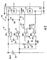
図2に、図1のシステムをより詳細に示す。図から、MEMSデバイス14が2つのMEMSスイッチ15,17を具備し、かつMEMSデバイス24がMEMSスイッチ23,25を具備することが見て取れる。このとき、バイアス回路28は、コンデンサ50と、可変コンダクタンススイッチ30とを具備する。可変コンダクタンススイッチ30は、CMOSトランジスタ52と、電流制限抵抗器54とを具備する。
FIG. 2 shows the system of FIG. 1 in more detail. From the figure, it can be seen that the
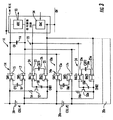
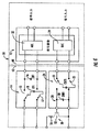
図3には、その構造が単純に反復される多数のバッテリーセル20〜20nを用いること、複数のバッテリーセルから出力電圧を供給するために、同一のホールドコンデンサ16を用い、かつフライングコンデンサ26〜26nに入力電圧を供給するために、同一のDAC 34を用いることが示されている。図4には、本発明のうちの一実施形態の物理的構造が示されている。ここで、信号調整回路12及びMEMSスイッチングデバイス14,24は、SOIチップなどの単一チップ58上にマウントされているか、又は、それらは、互いに隣接し、かつワイヤボンドによって相互に接続された、CMOSチップ60上に形成された信号調整回路12と、SOIチップ62上に形成されたMEMSスイッチ14,24とを用いた2つのチップ60,62であってもよい。ガルバニック絶縁信号調整システム及びMEMS構造のより詳細な開示は、同一出願人によって2004年12月6日に出願され、同一の譲渡人を有する米国特許出願第11/005,608号に示される。この引用によって、その全内容が本明細書に組み込まれる。
FIG. 3 shows the use of a large number of
本発明の具体的な特徴がいくつかの図に示され、かついくつかは示されなかったが、これは、便宜上のことであり、各特徴は、発明によるいくつかの又はすべての他の特徴と組み合わされてよい。明細書中で使用された用語「具備する、有する(including,comprising,having,with)」は、広範かつ包括的に解釈され、いかなる物理的相互接続にも限定されない。さらに、本出願に開示された実施形態だけが実現可能な実施形態であると受け取ってはならない。 While specific features of the invention have been shown in some drawings and some have not been shown, this is for convenience and each feature may include some or all other features according to the invention. May be combined. As used herein, the term “including, having, having, with” is to be interpreted broadly and comprehensively and is not limited to any physical interconnection. Further, it should not be taken that only the embodiments disclosed in this application are feasible embodiments.
さらに、この特許に対し、特許出願審査の間に提出されたあらゆる補正は、以下のような出願の形で提出されたあらゆる請求項の権利範囲の放棄を意図しない。すなわち、当業者はすべての考えうる均等物を完全に包含する特許請求の範囲を作成することを合理的に予期できないこと、多くの均等物は、補正の時点では予測不可能であり、(どちらかと言えば)何を放棄すべきかの正しい解釈を越えること、補正の根拠は、多数の均等物とのわずかな関係しか有さないこと、及び/又は、出願人が補正された任意の請求項に対するある実質的でない置換を記載することを予期できない多くの理由が存在することは明らかである。 Further, any amendments filed during the patent application examination for this patent are not intended to waive any claim scope filed in the form of an application such as: That is, one skilled in the art cannot reasonably anticipate creating a claim that fully encompasses all possible equivalents, many equivalents are unpredictable at the time of amendment, If anything) beyond the correct interpretation of what should be abandoned, the basis for the amendment has only a small relationship with a number of equivalents, and / or any claims amended by the applicant It is clear that there are many reasons why one cannot expect to describe certain non-substantial substitutions for.
その他の実施形態が当業者によって想起される。それらは添付の特許請求の範囲内にある。 Other embodiments will occur to those skilled in the art. They are within the scope of the appended claims.
10 ガルバニック絶縁信号調整システム
12 信号調整回路
14,24 MEMSデバイス
15,17,23,25 MEMSスイッチ
16 ホールドコンデンサ
18,26 フライングコンデンサ
20 バッテリーセル
22 ガルバニック絶縁充電平衡システム
28 バイアス回路
30 可変コンダクタンススイッチ
32 アナログ−デジタル変換部(ADC)
34 デジタル−アナログ変換部(DAC)
36 制御部
40 スイッチ
42 電流供給源
44 ライン
50 コンデンサ
52 CMOSトランジスタ
54 電流制限抵抗器
58 シングルチップ
60 CMOSチップ
62 SOIチップ
DESCRIPTION OF
34 Digital-to-analog converter (DAC)
36
Claims (9)
各セルに関連した平衡化回路と、
ガルバニック絶縁MEMSスイッチングデバイスと
を具備し、
各平衡化回路は、フライングコンデンサと、可変コンダクタンススイッチと、該可変コンダクタンススイッチのためのバイアス回路とを具備し、
前記ガルバニック絶縁MEMSスイッチングデバイスは、前記フライングコンデンサを電圧供給源と前記バイアス回路とに選択的に接続し、
前記電圧供給源に接続された場合、前記フライングコンデンサは所定の電圧に充電され、
前記バイアス回路に接続された場合、関連するセルの充電状態を所定のレベルに調整するように、前記可変コンダクタンススイッチが設定されることを特徴とするガルバニック絶縁充電平衡システム。A galvanically isolated charge balancing system for multi-cell batteries,
A balancing circuit associated with each cell;
A galvanic insulated MEMS switching device;
Each balancing circuit includes a flying capacitor, a variable conductance switch, and a bias circuit for the variable conductance switch,
The galvanic isolation MEMS switching device selectively connects the flying capacitor to a voltage supply source and the bias circuit;
When connected to the voltage supply source, the flying capacitor is charged to a predetermined voltage,
The galvanic insulated charge balancing system, wherein when connected to the bias circuit, the variable conductance switch is set to adjust the charge state of the associated cell to a predetermined level.
各セルに関連した平衡化回路と、
ガルバニック絶縁MEMSスイッチングデバイスと
を具備し、
各平衡化回路は、フライングコンデンサと、可変コンダクタンススイッチと、該可変コンダクタンススイッチのためのバイアス回路とを具備し、
前記ガルバニック絶縁MEMSスイッチングデバイスは、前記フライングコンデンサを電圧供給源と前記バイアス回路とに選択的に接続し、
前記電圧供給源に接続された場合、前記フライングコンデンサは所定の電圧に充電され、
前記バイアス回路に接続された場合、関連するセルを所定のレベルに放電するように、前記可変コンダクタンススイッチが設定されることを特徴とするガルバニック絶縁充電平衡システム。A galvanically isolated charge balancing system for multi-cell batteries,
A balancing circuit associated with each cell;
A galvanic insulated MEMS switching device;
Each balancing circuit includes a flying capacitor, a variable conductance switch, and a bias circuit for the variable conductance switch,
The galvanic isolation MEMS switching device selectively connects the flying capacitor to a voltage supply source and the bias circuit;
When connected to the voltage supply source, the flying capacitor is charged to a predetermined voltage,
The galvanic isolated charge balancing system, wherein the variable conductance switch is set to discharge an associated cell to a predetermined level when connected to the bias circuit.
各セルに関連した平衡化回路と、
ガルバニック絶縁MEMSスイッチングデバイスと
を具備し、
各平衡化回路は、フライングコンデンサと、可変コンダクタンススイッチと、該可変コンダクタンススイッチのためのバイアス回路とを具備し、
前記ガルバニック絶縁MEMSスイッチングデバイスは、前記フライングコンデンサを電圧供給源と前記バイアス回路とに選択的に接続し、
前記電圧供給源に接続された場合、前記フライングコンデンサは所定の電圧に充電され、
前記バイアス回路に接続された場合、関連するセルを所定のレベルに充電するように、前記可変コンダクタンススイッチが設定されることを特徴とするガルバニック絶縁充電平衡システム。A galvanically isolated charge balancing system for multi-cell batteries,
A balancing circuit associated with each cell;
A galvanic insulated MEMS switching device;
Each balancing circuit includes a flying capacitor, a variable conductance switch, and a bias circuit for the variable conductance switch,
The galvanic isolation MEMS switching device selectively connects the flying capacitor to a voltage supply source and the bias circuit;
When connected to the voltage supply source, the flying capacitor is charged to a predetermined voltage,
A galvanically isolated charge balancing system, wherein the variable conductance switch is set to charge the associated cell to a predetermined level when connected to the bias circuit.
Applications Claiming Priority (3)
| Application Number | Priority Date | Filing Date | Title |
|---|---|---|---|
| US11/657,824 | 2007-01-25 | ||
| US11/657,824 US7612537B2 (en) | 2007-01-25 | 2007-01-25 | Galvanically isolated charge balance system |
| PCT/US2008/000883 WO2008091640A2 (en) | 2007-01-25 | 2008-01-22 | Galvanically isolated charge balance system |
Publications (2)
| Publication Number | Publication Date |
|---|---|
| JP2010517504A JP2010517504A (en) | 2010-05-20 |
| JP5073760B2 true JP5073760B2 (en) | 2012-11-14 |
Family
ID=39645069
Family Applications (1)
| Application Number | Title | Priority Date | Filing Date |
|---|---|---|---|
| JP2009547284A Expired - Fee Related JP5073760B2 (en) | 2007-01-25 | 2008-01-22 | Galvanic isolated charging balance system |
Country Status (5)
| Country | Link |
|---|---|
| US (1) | US7612537B2 (en) |
| JP (1) | JP5073760B2 (en) |
| CN (1) | CN101627502B (en) |
| TW (1) | TWI352063B (en) |
| WO (1) | WO2008091640A2 (en) |
Families Citing this family (36)
| Publication number | Priority date | Publication date | Assignee | Title |
|---|---|---|---|---|
| JP5448408B2 (en) * | 2008-10-15 | 2014-03-19 | 三菱重工業株式会社 | Secondary battery control system |
| WO2011094348A1 (en) * | 2010-01-27 | 2011-08-04 | A123 Systems, Inc. | System and method providing power within a battery pack |
| US20110223468A1 (en) * | 2010-03-15 | 2011-09-15 | Electronvault, Inc. | Variable Energy System |
| US20110223458A1 (en) * | 2010-03-15 | 2011-09-15 | Electronvault, Inc. | Power Cell Array Receiver |
| US20110221398A1 (en) * | 2010-03-15 | 2011-09-15 | Electronvault, Inc. | Impedence Balancer |
| US20110279096A1 (en) * | 2010-05-17 | 2011-11-17 | Sonntag Jeffrey L | Method and apparatus for powering a high current system from a resistive electrical storage device |
| US8427107B2 (en) | 2010-06-22 | 2013-04-23 | A 123 Systems, Inc. | System and method for extending the usable capacity of a battery pack via controlling battery current through different current paths |
| US8541979B2 (en) | 2010-06-22 | 2013-09-24 | A123 Systems, Inc. | System and method for balancing voltage of individual battery cells within a battery pack |
| JP2012139088A (en) * | 2010-12-06 | 2012-07-19 | Seiko Instruments Inc | Cell balance device and battery system |
| WO2012127270A1 (en) | 2011-03-23 | 2012-09-27 | Indian Institute Of Technology Bombay | Photo-voltaic array fed switched capacitor dc-dc converter based battery charging for li-ion batteries |
| US20130062946A1 (en) * | 2011-09-14 | 2013-03-14 | Electronvault, Inc. | Hierarchical balancing system |
| CN103166272A (en) * | 2011-12-16 | 2013-06-19 | 财团法人金属工业研究发展中心 | High-pressure-difference type capacitance active balancing device and method thereof |
| EP2909875B1 (en) | 2012-10-16 | 2020-06-17 | Ambri Inc. | Electrochemical energy storage devices and housings |
| US9312522B2 (en) | 2012-10-18 | 2016-04-12 | Ambri Inc. | Electrochemical energy storage devices |
| US10541451B2 (en) | 2012-10-18 | 2020-01-21 | Ambri Inc. | Electrochemical energy storage devices |
| US9735450B2 (en) | 2012-10-18 | 2017-08-15 | Ambri Inc. | Electrochemical energy storage devices |
| US9520618B2 (en) | 2013-02-12 | 2016-12-13 | Ambri Inc. | Electrochemical energy storage devices |
| US11721841B2 (en) | 2012-10-18 | 2023-08-08 | Ambri Inc. | Electrochemical energy storage devices |
| US11211641B2 (en) | 2012-10-18 | 2021-12-28 | Ambri Inc. | Electrochemical energy storage devices |
| US11387497B2 (en) | 2012-10-18 | 2022-07-12 | Ambri Inc. | Electrochemical energy storage devices |
| US10270139B1 (en) | 2013-03-14 | 2019-04-23 | Ambri Inc. | Systems and methods for recycling electrochemical energy storage devices |
| US8901888B1 (en) | 2013-07-16 | 2014-12-02 | Christopher V. Beckman | Batteries for optimizing output and charge balance with adjustable, exportable and addressable characteristics |
| US9246407B2 (en) | 2013-03-29 | 2016-01-26 | General Electric Company | Voltage balancing system and method for multilevel converters |
| US9502737B2 (en) | 2013-05-23 | 2016-11-22 | Ambri Inc. | Voltage-enhanced energy storage devices |
| US12347832B2 (en) | 2013-09-18 | 2025-07-01 | Ambri, LLC | Electrochemical energy storage devices |
| DK3058605T3 (en) | 2013-10-16 | 2024-03-04 | Ambri Inc | SEALS FOR DEVICES OF REACTIVE HIGH TEMPERATURE MATERIAL |
| WO2015058165A1 (en) | 2013-10-17 | 2015-04-23 | Ambri Inc. | Battery management systems for energy storage devices |
| US12142735B1 (en) | 2013-11-01 | 2024-11-12 | Ambri, Inc. | Thermal management of liquid metal batteries |
| US10181800B1 (en) | 2015-03-02 | 2019-01-15 | Ambri Inc. | Power conversion systems for energy storage devices |
| WO2016141354A2 (en) | 2015-03-05 | 2016-09-09 | Ambri Inc. | Ceramic materials and seals for high temperature reactive material devices |
| US9893385B1 (en) | 2015-04-23 | 2018-02-13 | Ambri Inc. | Battery management systems for energy storage devices |
| CN109661367A (en) * | 2016-07-08 | 2019-04-19 | 罗伯特·博世有限公司 | Hybrid current for the encapsulation of micro-electromechanical system (MEMS) sensor component connects system |
| US11929466B2 (en) | 2016-09-07 | 2024-03-12 | Ambri Inc. | Electrochemical energy storage devices |
| CN110731027B (en) | 2017-04-07 | 2024-06-18 | 安保瑞公司 | Molten salt battery with solid metal cathode |
| WO2020131617A1 (en) | 2018-12-17 | 2020-06-25 | Ambri Inc. | High temperature energy storage systems and methods |
| US11501928B2 (en) | 2020-03-27 | 2022-11-15 | Menlo Microsystems, Inc. | MEMS device built on substrate with ruthenium based contact surface material |
Family Cites Families (8)
| Publication number | Priority date | Publication date | Assignee | Title |
|---|---|---|---|---|
| US4740966A (en) * | 1986-09-30 | 1988-04-26 | Texas Instruments Incorporated | Analog input circuit for microcontroller apparatus |
| CN1479426A (en) * | 2002-08-27 | 2004-03-03 | 何镇宇 | Natural balance charging control device |
| US7378818B2 (en) * | 2002-11-25 | 2008-05-27 | Tiax Llc | Bidirectional power converter for balancing state of charge among series connected electrical energy storage units |
| JP4035777B2 (en) * | 2003-02-10 | 2008-01-23 | 株式会社デンソー | Discharge device for battery pack |
| US6975193B2 (en) | 2003-03-25 | 2005-12-13 | Rockwell Automation Technologies, Inc. | Microelectromechanical isolating circuit |
| CN2625185Y (en) * | 2003-06-26 | 2004-07-14 | 武汉力兴测试设备有限公司 | Group battery module balancing unit of electric automobile |
| US7288940B2 (en) * | 2004-12-06 | 2007-10-30 | Analog Devices, Inc. | Galvanically isolated signal conditioning system |
| CN101039039A (en) * | 2006-03-13 | 2007-09-19 | 天津市民福热收缩材料厂 | Batteries charging balancing management system and its working method |
-
2007
- 2007-01-25 US US11/657,824 patent/US7612537B2/en active Active
-
2008
- 2008-01-22 JP JP2009547284A patent/JP5073760B2/en not_active Expired - Fee Related
- 2008-01-22 CN CN2008800030048A patent/CN101627502B/en not_active Expired - Fee Related
- 2008-01-22 WO PCT/US2008/000883 patent/WO2008091640A2/en not_active Ceased
- 2008-01-25 TW TW097102938A patent/TWI352063B/en not_active IP Right Cessation
Also Published As
| Publication number | Publication date |
|---|---|
| CN101627502B (en) | 2012-05-30 |
| US20080180063A1 (en) | 2008-07-31 |
| JP2010517504A (en) | 2010-05-20 |
| TW200840794A (en) | 2008-10-16 |
| TWI352063B (en) | 2011-11-11 |
| CN101627502A (en) | 2010-01-13 |
| WO2008091640A2 (en) | 2008-07-31 |
| WO2008091640A3 (en) | 2008-10-09 |
| US7612537B2 (en) | 2009-11-03 |
Similar Documents
| Publication | Publication Date | Title |
|---|---|---|
| JP5073760B2 (en) | Galvanic isolated charging balance system | |
| US9240685B2 (en) | Reconfigurable matrix-based power distribution architecture | |
| JP3655171B2 (en) | Charge / discharge control circuit and secondary battery device | |
| KR101785734B1 (en) | Mosfet circuit comprising a switch of switching-type cell voltage balancing circuit having series-parallel circuit, and driving circuit thereof | |
| US7863863B2 (en) | Multi-cell battery pack charge balance circuit | |
| CA2703788C (en) | Power supply controller | |
| KR102237034B1 (en) | Balancing apparatus and the method supporting various balancing operation modes | |
| JPWO2015029283A1 (en) | Battery controller | |
| JP4491917B2 (en) | Battery pack | |
| US20160036251A1 (en) | Quick low-voltage rechargeable battery | |
| JP2009247145A (en) | Power system | |
| US9136713B1 (en) | Proactive and highly efficient active balance apparatus for a battery power system | |
| JP2015186331A (en) | balance correction circuit, power storage module and balance correction method | |
| KR20190048972A (en) | Starting battery system for cell balancing of Lithium battery pack and capacitor | |
| JP2022536028A (en) | Reconfigurable power processing unit for spacecraft operation | |
| WO2019179787A8 (en) | Converter | |
| WO2006058028A3 (en) | High-energy battery power source for implantable medical use | |
| JP2017052446A5 (en) | ||
| WO2018117387A3 (en) | Voltage detection integrated circuit and battery management system including same | |
| CN108400394B (en) | Electronic switchgear for battery management system and battery | |
| CN102017274A (en) | Energy storage | |
| US20240178678A1 (en) | Control of an energy storage arrangement | |
| JP2006246595A (en) | Secondary battery pack | |
| US12155262B2 (en) | Method and apparatus for reducing the inrush current of an implanted electrical device | |
| CN111619398B (en) | Unit module and method for operating a unit module |
Legal Events
| Date | Code | Title | Description |
|---|---|---|---|
| A621 | Written request for application examination |
Free format text: JAPANESE INTERMEDIATE CODE: A621 Effective date: 20101220 |
|
| TRDD | Decision of grant or rejection written | ||
| A01 | Written decision to grant a patent or to grant a registration (utility model) |
Free format text: JAPANESE INTERMEDIATE CODE: A01 Effective date: 20120724 |
|
| A01 | Written decision to grant a patent or to grant a registration (utility model) |
Free format text: JAPANESE INTERMEDIATE CODE: A01 |
|
| A61 | First payment of annual fees (during grant procedure) |
Free format text: JAPANESE INTERMEDIATE CODE: A61 Effective date: 20120822 |
|
| R150 | Certificate of patent or registration of utility model |
Ref document number: 5073760 Country of ref document: JP Free format text: JAPANESE INTERMEDIATE CODE: R150 Free format text: JAPANESE INTERMEDIATE CODE: R150 |
|
| FPAY | Renewal fee payment (event date is renewal date of database) |
Free format text: PAYMENT UNTIL: 20150831 Year of fee payment: 3 |
|
| R250 | Receipt of annual fees |
Free format text: JAPANESE INTERMEDIATE CODE: R250 |
|
| R250 | Receipt of annual fees |
Free format text: JAPANESE INTERMEDIATE CODE: R250 |
|
| R250 | Receipt of annual fees |
Free format text: JAPANESE INTERMEDIATE CODE: R250 |
|
| R250 | Receipt of annual fees |
Free format text: JAPANESE INTERMEDIATE CODE: R250 |
|
| R250 | Receipt of annual fees |
Free format text: JAPANESE INTERMEDIATE CODE: R250 |
|
| R250 | Receipt of annual fees |
Free format text: JAPANESE INTERMEDIATE CODE: R250 |
|
| R250 | Receipt of annual fees |
Free format text: JAPANESE INTERMEDIATE CODE: R250 |
|
| LAPS | Cancellation because of no payment of annual fees |