JP2009201345A - Battery cell balancing system using current regulator - Google Patents
Battery cell balancing system using current regulator Download PDFInfo
- Publication number
- JP2009201345A JP2009201345A JP2008330833A JP2008330833A JP2009201345A JP 2009201345 A JP2009201345 A JP 2009201345A JP 2008330833 A JP2008330833 A JP 2008330833A JP 2008330833 A JP2008330833 A JP 2008330833A JP 2009201345 A JP2009201345 A JP 2009201345A
- Authority
- JP
- Japan
- Prior art keywords
- cell
- current
- cells
- voltage
- bypass path
- Prior art date
- Legal status (The legal status is an assumption and is not a legal conclusion. Google has not performed a legal analysis and makes no representation as to the accuracy of the status listed.)
- Pending
Links
Images


Classifications
-
- Y—GENERAL TAGGING OF NEW TECHNOLOGICAL DEVELOPMENTS; GENERAL TAGGING OF CROSS-SECTIONAL TECHNOLOGIES SPANNING OVER SEVERAL SECTIONS OF THE IPC; TECHNICAL SUBJECTS COVERED BY FORMER USPC CROSS-REFERENCE ART COLLECTIONS [XRACs] AND DIGESTS
- Y02—TECHNOLOGIES OR APPLICATIONS FOR MITIGATION OR ADAPTATION AGAINST CLIMATE CHANGE
- Y02E—REDUCTION OF GREENHOUSE GAS [GHG] EMISSIONS, RELATED TO ENERGY GENERATION, TRANSMISSION OR DISTRIBUTION
- Y02E60/00—Enabling technologies; Technologies with a potential or indirect contribution to GHG emissions mitigation
- Y02E60/10—Energy storage using batteries
Landscapes
- Charge And Discharge Circuits For Batteries Or The Like (AREA)
- Secondary Cells (AREA)
Abstract
Description
本発明は、電池保護システムに関する。さらに詳しくは、電池セルバランシングシステムに関する。 The present invention relates to a battery protection system. More specifically, the present invention relates to a battery cell balancing system.
この出願は、2007年10月9日に出願した米国仮特許出願第60/998,104号の優先権を主張する。これを引用することによりその全体が本明細書に組み込まれる。 This application claims priority from US Provisional Patent Application No. 60 / 998,104, filed Oct. 9, 2007. This is incorporated herein by reference in its entirety.
DC電圧電源として使用される典型的なリチウム・イオン(Li-Ion)バッテリパックは、通常、直列に接続された電池セルのグループを具備している。 A typical lithium-ion (Li-Ion) battery pack used as a DC voltage power supply usually comprises a group of battery cells connected in series.
通常操作により前記バッテリパックの充電および放電を長期間にわたり繰り返していると、セル間のセル電圧に変動が現れる。直列接続された一連の(in a series string)1つまたは複数のセルは、他に比べて充電が早かったり遅かったりするため、アンバランスな状態となる。 If charging and discharging of the battery pack are repeated over a long period of time through normal operation, fluctuations in cell voltage between cells appear. One or more cells in a series string connected in series are unbalanced because they charge faster or slower than others.
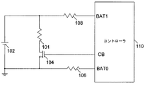
図1は、外部のバイパス経路を制御するための専用のピン(pin)を使用した従来のセルバランシング回路を示している。セル102の正極(アノード)は、第1抵抗器108を介してコントローラ110のBAT1端子に接続されている。セル102の負極(カソード)は、第2抵抗器106を介してコントローラ110のBAT0端子に接続されている。外部のバイパス経路は、セル102に並列接続されている。前記バイパス経路は、電流制限抵抗器(current limiting resistor)101を具備し、放出(bleeding)コントロールスイッチ104は、前記電流制限抵抗器101に直列に接続されている。前記スイッチ104は、専用ピンCBを介してコントローラ110により制御される。
FIG. 1 shows a conventional cell balancing circuit using a dedicated pin for controlling an external bypass path. The positive electrode (anode) of the
アンバランス状態が発生したとき、例えば、セル102の電圧が、前記バッテリパックの他のセル(簡潔化と明瞭性のために図1には示していない)よりも大きいときには、前記コントローラ110は、放出電流が外部バイパスを通って流れるようにイネーブルするための前記スイッチ104をオンにする。その結果、前記バッテリパックのセル電圧のバランシングが図れる。この方法のひとつの欠点は、放出コントロールスイッチ104への余分なCBピンが必要となることから費用が増加しうるということである。
When an unbalanced condition occurs, for example, when the voltage of
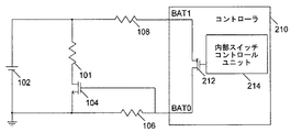
図2は、放出コントロールスイッチの制御に内部スイッチを使用する他の従来のセルバランシング回路を示している。図1と同じ符号付の要素は同様の機能を有するので、簡潔化と明瞭性のために本明細書では繰り返し説明しない。コントローラ210内部において、内部スイッチ212は、BAT1端子とBAT0端子間に接続されている。前記内部スイッチは、同様にコントローラ210内部にある内部スイッチコントロールユニット214により制御されている。
FIG. 2 shows another conventional cell balancing circuit that uses an internal switch to control the emission control switch. Elements that are labeled the same as in FIG. 1 have similar functions and will not be repeated here for the sake of brevity and clarity. Inside the
図2において、抵抗器106での電圧降下は、放出コントロールスイッチ104のコンダクタンスステータスを決定する。さらに、内部スイッチ212が内部スイッチコントロールユニット214からのコントロール信号によりオンとなるとき、前記抵抗器106での電圧降下は、抵抗器108および抵抗器106を具備する分圧器により決定される。抵抗器106の電圧降下自体は小さい(例えばセル電圧の半分)。
In FIG. 2, the voltage drop across
この方法には他にもいくつかの欠点がある。第1に、前記抵抗器106の電圧降下が小さいため、放出コントロールスイッチ104が抵抗器106における小さな電圧降下でもオンできるように放出コントロールスイッチ104の閾値電圧を十分に低くなければならない(例えば1Vなど)。もし、前記放出コントロールスイッチ104がMOSFETであるならば、低い閾値電圧のMOSFETである必要がありうる。そのようなMOSFETは、一般に高価であり、回路の総費用を増加させてしまう。
There are several other disadvantages to this method. First, because the voltage drop across the
第2に、直列に接続されたセルのグループの場合を考えると、近傍のセルの放出コントロールスイッチは、同時にはイネーブル(enabled)にできないため、セルグループを有するバッテリパックのための前記バランシング回路の実際使用を制限する原因となる。図2においては、バイパス経路を形成するために、内部スイッチ212がオンされBAT0端子から抵抗器106を通りセル102の負極に電流が流れる。もしセル102に直列に接続された第2セル(簡潔化と明瞭性のために図2には示していない)が存在した場合、前記抵抗器106は、第2セルの正極とコントローラ210の間に接続される。第2セルのバイパス経路を形成する(conduct)ためには、放出電流は、第2セルの正極から前記抵抗器106を通ってBAT0端子に流れることが必要となるが、それは電流方向の衝突の結果をもたらす。
Second, considering the case of a group of cells connected in series, the discharge control switches of neighboring cells cannot be enabled at the same time, so that the balancing circuit for a battery pack having a cell group can be It becomes the cause which restricts actual use. In FIG. 2, in order to form a bypass path, the
第3に、前記セル電圧は、前記放出コントロールスイッチ104が確実に操作可能となりうるだけ十分に高い必要がある。もしセル電圧がかなり低い場合には、前記放出コントロールスイッチ104のゲートからソース間の電圧Vgs(それは、前記抵抗器106の電圧降下である)は、前記放出コントロールスイッチ104の閾値電圧よりも決して大きくはならない。たとえ内部スイッチ212がオンしてもスイッチ104それ自体がオンしない。したがって、この方法はLiFePo4セルのような低電圧セルには適用できない。
Third, the cell voltage needs to be high enough that the
本発明の一構成によれば、セルをバランシングするために使用されるセルバランシング回路が提供される。前記セルバランシング回路は、セルに接続されたバイパス経路と、前記バイパス経路に接続された電流レギュレータと、放出コントロールスイッチと、を具備する。前記電流レギュレータは、電流を生成するとともに前記バイパス経路のコンダクタンスステータスを制御することが可能である。前記放出コントロールスイッチは、前記電流レギュレータにより生成される電流に応じて前記バイパス経路を形成する(conduct)。 According to one configuration of the present invention, a cell balancing circuit used to balance cells is provided. The cell balancing circuit includes a bypass path connected to the cell, a current regulator connected to the bypass path, and a discharge control switch. The current regulator can generate a current and control a conductance status of the bypass path. The discharge control switch forms the bypass path according to a current generated by the current regulator.
本発明の実施形態における機能および利点は、符号で要素を示している図面を参照しながらの以下の詳細な記載により明白になる。 The features and advantages of embodiments of the present invention will become apparent from the following detailed description when taken in conjunction with the drawings, in which the elements are designated by reference numerals.
本明細書には、いくつかの本発明の実施形態が詳細になされている。本発明は、これらの実施形態とともに説明されているが、本発明をこれらの実施形態に限定する目的ではないことは、理解されよう。開示された本発明の付加的な利点および特徴は、以下の詳細な説明から当業者にとって自明である。説明するように、本開示により、本開示の精神から逸脱することなくすべてのあらゆる点から修正可能となる。従って図面と記載は、説明のためのものであり、限定するためのものではない。 In the present specification, several embodiments of the present invention are described in detail. While the invention has been described in conjunction with these embodiments, it will be understood that it is not intended to limit the invention to these embodiments. Additional advantages and features of the disclosed invention will be apparent to those skilled in the art from the following detailed description. As will be described, the present disclosure can be modified in all respects without departing from the spirit of the present disclosure. Accordingly, the drawings and descriptions are for purposes of illustration and not limitation.
図3は、機能モジュール302と、バッテリパック304と、を具備する電気システム300を示している。前記バッテリパック304は、電池セルのグループを有する。前記機能モジュール302は、前記バッテリパック304を備えるとともに、1つまたは複数の機能を実行可能である。前記電気システム300は、コンピュータシステム,車,電気バイク,無停電電源装置などであってよいが、それらに限定されない。一実施形態では、前記機能モジュール302は、コンピュータシステムの中央演算処理装置(CPU)を備える。一実施形態では、前記機能モジュール302は、車のモータ(vehicle motor)である。
FIG. 3 shows an
本発明によると、一実施形態では、ピン数を減らすとともに、バッテリセル電圧が低くても動作可能な前記バッテリパック304のための電池セルバランシング回路が提供される。一実施形態では前記セルバランシング回路は、バッテリセルのバイパス経路を制御するのに電流レギュレータを使用する。電池セルのバイパス経路を形成するための放出コントロールスイッチは、さまざまなスイッチの型であってよく、低閾値電圧(例えば1Vなど)のスイッチに限定されないことが有利である。さらに、一実施形態では、前記電池セルバランシング回路は、例えば隣接セルを同時にバランスさせるなど多数のセルを同時にバランスさせることが可能である。
According to the present invention, in one embodiment, a battery cell balancing circuit is provided for the
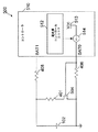
図4は、本発明における一実施形態のセルバランシング回路400を示している。図4の一実施形態における前記バランシング回路400は、セル102のバイパス経路のコンダクタンスステータスを制御するために、例えば内部電流シンク(sink)414などといった定電流レギュレータを使用している。一実施形態においては、前記電流レギュレータ414は、前記バイパス経路のコンダクタンスステータスを制御するための電流を生成するために前記バイパス経路に接続されている。一実施形態においては、前記バイパス経路は、前記電流レギュレータ414により生成される電流に応じて形成される(オンされる)。
FIG. 4 shows a
バッテリパックにおける前記セル102の正極(アノード)は、第1抵抗器408を介してコントローラ410のBAT1端子に接続されている。前記セル102の負極(カソード)は、第2抵抗器406を介して前記コントローラ410のBAT0端子に接続されている。バイパス経路は、前記セル102のバイパス電流をイネーブルするために前記セル102に並列に接続されている。
The positive electrode (anode) of the
一実施形態において、前記バイパス経路は、放出(バランシング)コントロールスイッチ404を備えるとともに、電流制限抵抗器401と直列に接続されている。一実施形態において、前記放出コントロールスイッチ404は、P型金属酸化膜半導体電界効果トランジスタ(PMOSFET)であってよい。前記放出コントロールスイッチ404は、前記電流レギュレータ414により生成される電流に応じて前記バイパス経路を形成することができる。一実施形態において、前記抵抗器408は、前記バイパス経路と前記電流シンク414の間に接続されている。前記放出コントロールスイッチ404のコンダクタンスステータスは、図4の例における抵抗器408での電圧降下に等しいゲート−ソース間電圧Vgsにより決定される。一実施形態においては、コントローラ410は、前記バッテリパックの充電および/または放電を制御するために使用されるとともに、前記バッテリパックのための保護機能(例えば、過電圧保護,過電流保護,低電圧保護,セルのバランシングなど)を果たしている。前記コントローラ410は、前記バッテリパックに組み込んでもよい。前記コントローラ410は、BAT1端子とグランドの間に接続された電流シンク414のような電流レギュレータを備えてもよい。前記電流シンク414は、前記セル102の正極から前記抵抗器408を介しグランドへ流れるシンク電流を提供するために使用可能であるとともに、前記バイパス経路のコンダクタンスステータスをコントロールするために使用可能である。言い換えれば、電流シンク414は、前記セル102の正極から電流をシンクする。前記シンク電流は、前記抵抗器408を介して流れるため、それにより前記抵抗器408での電圧降下を引き起こす。そのように(as such)、前記バイパス経路のコンダクタンスステータスは、前記抵抗器408の電圧降下により決定されうる。
In one embodiment, the bypass path comprises a discharge (balancing)
前記コントローラ410は、電流シンク414をコントロール(例えばイネーブル/ディスエーブル)するために使用可能な電流シンクコントロールユニット412をさらに具備する。一実施形態において、前記電流シンクコントロールユニット412は、前記セル102をモニターするとともに、もしセル102がアンバランスならば電流シンク414をイネーブルにする。一実施形態において、もしセル102の電圧が所定の閾値よりも大きい場合にはセル102はアンバランスである。他の実施形態において、同一バッテリパック内におけるセル102の電圧と他のセル(簡略化と明確化のために図4には示していない)の電圧差が所定の閾値よりも大きい場合には、セル102はアンバランスである。他の実施形態において、前記セル102の前記バイパス経路は、前記コントローラ410の内部に構築してもよい。
The
図示するために、前記抵抗器408の抵抗は1 KΩ,電流シンク414により供給される前記シンク電流は3 mA,そして前記放出コントロールスイッチ404の閾値電圧は-1 Vであると仮定した。しかし、本開示における前記セルバランシング回路は、そのような特定の値に限定されるものではない。
For purposes of illustration, it was assumed that the resistance of
操作中に、もしアンバランス状態が発生した場合(例えば、前記バッテリパックの充電/放電/待機段階中)には、前記電流シンク414は、前記セル102の正極から前記抵抗器408を介してグランドへ流れるシンク電流、例えば3 mA、を提供するように前記電流シンクコントロールユニット412によりイネーブルされる。前述のように、前記抵抗器408における電圧降下は3 Vである。従って、一実施形態において、前記放出コントロールスイッチ404のゲート-ソース間電圧Vgsは、-3 Vであり、前記放出コントロールスイッチ404は、オンされる。ひとたび前記放出コントロールスイッチ404がオンされると、対応するバイパス経路が形成される(オンされる)。その結果、放出電流(バランシング電流)は前記バイパス経路を通って流れ、前記バッテリパックのセル電圧をバランシングする。例えば電池の充電段階の間、もし放出電流が前記セル102のためにイネーブルとなれば、前記セル102の充電電流の一部は前記バイパス経路を介して分路され、従って前記セル102の充電速度が落ちるため、セルのアンバランスは、一定時間のバランシング後には減少/解消される。一実施形態においては、その一定時間は前記電流シンクコントロールユニット412により決定される。
During operation, if an unbalanced condition occurs (e.g., during the charge / discharge / standby phase of the battery pack), the
図5には、本発明の一実施形態におけるセルバランシング回路500が図示されている。図4と同じ符号の要素は同様の機能を有し、簡潔化と明瞭性のためにここでは詳細に説明しない。一実施形態において、図5におけるバランシング回路500は、バッテリパック内のセル102のバイパス経路におけるコンダクタンスステータスを制御するために、例えば内部電流源514といった定電流レギュレータを使用している。一実施形態において、前記電流レギュレータ514は、前記バイパス経路のコンダクタンスステータスを制御する電流を生成するために前記バイパス経路に接続されている。一実施形態において、前記バイパス経路は、前記電流源514により生成された電流に応じて形成される(オンする)。
FIG. 5 illustrates a
一実施形態においては、放出コントロールスイッチ504は、N型金属酸化膜半導体電界効果トランジスタ(NMOSFET)であってよい。前記放出コントロールスイッチ504は、電流レギュレータ514により生成された電流に応じて前記バイパス経路を形成する。前記セル102の正極は、第1抵抗器408を介してコントローラ510のBAT1端子に接続されている。前記セル102の前記負極は、第2抵抗器406を介して前記コントローラ510のBAT0端子に接続されている。前記放出コントロールスイッチ504のコンダクタンスステータスは、図5に例示した前記抵抗器406における電圧降下に等しいゲート-ソース間電圧Vgsにより決定される。一実施形態において、前記コントローラ510は、前記バッテリパックの充電および/または放電を制御するために使用されるとともに、前記バッテリパックのための保護機能(例えば、過電圧保護,過電流保護,低電圧保護,セルのバランシングなど)を果している。前記コントローラ510は、前記バッテリパックに組み込んでもよい。一実施形態において、前記コントローラ510は、BAT0端子と電力源Vcc513の間に接続された電流源514を備えてもよい。前記電流源514は、電力源513から前記抵抗器406を介して前記セル102の前記負極へ流れるソース電流を提供するために使用可能であるとともに、前記バイパス経路のコンダクタンスステータスをコントロールするためにも使用可能である。言い換えれば、前記電流源514は、前記セル102の前記負極への電流のソースである。前記ソース電流は、前記抵抗器406を流れるため、前記抵抗器406において電圧降下を生じさせる。前述のように、前記バイパス経路のコンダクタンスステータスは、前記抵抗器406にわたる電圧降下により決定されうる。
In one embodiment, the
前記コントローラ510は、前記電流源514をコントロールするため(例えば、イネーブル/ディスエーブル)に使用可能な電流源コントロールユニット512をさらに具備する。一実施形態において、前記電流源コントロールユニット512は、前記セル102をモニターし、もしセル102がアンバランスならば前記電流源514をイネーブルする。一実施形態において、もしセル102の電圧が所定の閾値よりも大きい場合にはセル102はアンバランスである。他の実施形態において、同一バッテリパック内におけるセル102の電圧と他のセル(簡略化と明確化のために図5には示していない)の電圧差が所定の閾値よりも大きい場合には、セル102はアンバランスである。他の実施形態において、前記セル102の前記バイパス経路は、前記コントローラ510の内部に構築してもよい。
The
図示するために、抵抗器406の抵抗は1 KΩ,前記電流源514により提供されるソース電流は3 mA,そして前記放出コントロールスイッチ504の閾値電圧は1 Vであると仮定した。しかし、本開示における前記セルバランシング回路は、そのような特定の値に限定されるものではない。
For purposes of illustration, it was assumed that the resistance of
もしアンバランス状態が発生した場合には、電力源513から前記抵抗器406を通って前記セル102の前記負極へ流れるソース電流、例えば3 mA、を提供するように、前記電流源514は、前記電流源コントロールユニット512によりイネーブルされる。前述したように、前記抵抗器406における前記電圧降下は3 Vである。したがって、一実施形態において、前記放出コントロールスイッチ504のゲート-ソース間電圧Vgsは、3 Vであり、前記放出コントロールスイッチ504は、オンされる。ひとたび前記放出コントロールスイッチ504がオンされると、対応するバイパス経路が形成される(オンされる)。その結果、放出電流(バランシング電流)は前記バイパス経路を介して流れ、前記バッテリパックのセル電圧をバランシングする。一実施形態においては、放出時間は、電流源コントロールユニット512により決定される。
If an unbalance condition occurs, the
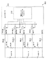
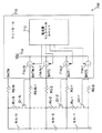
図6は、本発明の一実施形態におけるバッテリパック内の直列接続されたセルのグループであるセル-1からセル-Nのバランシングのためのセルバランシング回路を示している。セル-1〜セル-Nは、直列に接続されている。簡潔化と明瞭性のために前記セルのすべてが図6に示されているわけではない。複数のバイパス経路は、それぞれ前記セルのセル-1〜セル-Nに接続されており、複数のバイパス経路のそれぞれは、対応するセルのバイパス電流をイネーブルするために使用可能である。一実施形態において、それぞれのバイパス経路は、対応する放出コントロールスイッチQ1-1〜Q1-Nおよび直列に接続された対応する抵抗器Rc-1〜Rc-Nを具備する。したがって、バイパス経路のコンダクタンスステータスは、対応する放出コントロールスイッチQ1-1〜Q1-Nのコンダクタンスステータスにより決定される。それぞれの前記放出コントロールスイッチQ1-1〜Q1-Nは、PMOSFETであってよい。簡潔化および明瞭性のために、すべての前記放出コントロールスイッチおよび抵抗器が図6に示されているわけではない。 FIG. 6 shows a cell balancing circuit for balancing cells-1 to cell-N, which are groups of cells connected in series in a battery pack according to an embodiment of the present invention. Cell-1 to cell-N are connected in series. Not all of the cells are shown in FIG. 6 for simplicity and clarity. A plurality of bypass paths are respectively connected to the cell-1 to cell-N of the cell, and each of the plurality of bypass paths can be used to enable a bypass current of a corresponding cell. In one embodiment, each bypass path comprises a corresponding discharge control switch Q1-1 to Q1-N and a corresponding resistor Rc-1 to Rc-N connected in series. Therefore, the conductance status of the bypass path is determined by the conductance status of the corresponding discharge control switches Q1-1 to Q1-N. Each of the emission control switches Q1-1 to Q1-N may be a PMOSFET. For simplicity and clarity, not all the emission control switches and resistors are shown in FIG.
コントローラ610は、複数のセルのセル-1〜セル-Nをバランシングするために複数のセルのセル-1〜セル-Nに接続されている。前記コントローラ610は、例えば電流シンク614-1〜614-Nといった複数の電流レギュレータを具備し、複数のバイパス経路にそれぞれ接続されている。複数の電流レギュレータ614-1〜614-Nのそれぞれは、対応するバイパス経路のコンダクタンスステータスを制御するための、対応するセルの正極からグランドへ流れる電流を生成するのに使用可能である。前記対応するバイパス経路は、前記電流に応じて形成される(オンされる)。それぞれの放出コントロールスイッチQ1-1〜Q1-Nは、対応する電流レギュレータ614-1〜614-Nから生成された電流に応じて、対応するバイパス経路を形成される(オンする)。前記セルセル-1〜セル-Nの端子は、前記コントローラ610の端子BAT0〜BATNにそれぞれ抵抗器R0-0〜R0-Nを介して接続されている。一実施形態において、端子BAT1〜BATNは、前記コントローラ610の電流シンク614-1〜614-Nを介してグランドに接続されている。簡潔化および明瞭性のために、すべての端子,抵抗器,および電流シンクが図6に示されているわけではない。一実施形態において、複数の電流レギュレータ614-1〜614-Nのそれぞれは、対応する抵抗器R0-0〜R0-N-1を流れる電流を生成するために使用可能であり、対応する抵抗器R0-0〜R0-N-1における電圧降下を生じる。一実施形態において、対応する放出コントロールスイッチQ1-1〜Q1-Nの前記コンダクタンスステータスは、対応する抵抗器R0-0〜R0-N-1における電圧降下により決定される。
一実施形態において、前記コントローラ610は、電流シンク614-1〜614-Nをコントロールするために使用可能な電流シンクコントロールユニット612を具備してもよい。一実施形態において、もし対応するセルのセル-1〜セル-Nがアンバランスならば、前記コントローラ610内の前記電流シンクコントロールユニット612は、対応する電流シンク614-1〜614-Nをイネーブルする。前記電流シンク614-1〜614-Nは、前記電流シンクコントロールユニット612により個別にまたは同時にイネーブルまたはディスエーブルされる。したがって、前記バランシング回路はそれぞれのセルの状態に従ってセルのグループをバランシングするために使用可能である。
In one embodiment, the
図7は、本発明の一実施形態におけるバッテリパック内の直列接続されたセルのグループであるセル-1〜セル-Nをバランシングするためのセルバランシング回路を示している。セル-1〜セル-Nは、直列に接続されている。簡潔化と明瞭性のために前記セルのすべてが図6に示されているわけではない。複数のバイパス経路は、それぞれ前記セルのセル-1〜セル-Nに接続されており、複数のバイパス経路のそれぞれは、対応するセルのバイパス電流をイネーブルするために使用可能である。一実施形態において、それぞれのバイパス経路は、対応する放出コントロールスイッチQ1-1〜Q1-Nおよび直列に接続された抵抗器Rc-1〜Rc-Nを具備する。したがって、バイパス経路のコンダクタンスステータスは、対応する放出コントロールスイッチQ1-1〜Q1-Nのコンダクタンスステータスにより決定される。それぞれの前記放出コントロールスイッチQ1-1〜Q1-Nは、NMOSFETであってよい。簡潔化および明瞭性のために、すべての前記放出コントロールスイッチおよび抵抗器が図7に示されているわけではない。 FIG. 7 shows a cell balancing circuit for balancing cells-1 to cell-N, which are groups of cells connected in series in a battery pack according to an embodiment of the present invention. Cell-1 to cell-N are connected in series. Not all of the cells are shown in FIG. 6 for simplicity and clarity. A plurality of bypass paths are respectively connected to the cell-1 to cell-N of the cell, and each of the plurality of bypass paths can be used to enable a bypass current of a corresponding cell. In one embodiment, each bypass path comprises a corresponding emission control switch Q1-1 to Q1-N and resistors Rc-1 to Rc-N connected in series. Therefore, the conductance status of the bypass path is determined by the conductance status of the corresponding discharge control switches Q1-1 to Q1-N. Each of the emission control switches Q1-1 to Q1-N may be an NMOSFET. For simplicity and clarity, not all the emission control switches and resistors are shown in FIG.
コントローラ710は、複数のセルのセル-1〜セル-Nをバランシングするために複数のセルのセル-1〜セル-Nに接続されている。前記コントローラ710は、例えば電流源714-1〜714-Nといった複数の電流レギュレータを具備し、複数のバイパス経路にそれぞれ接続されている。複数の電流レギュレータ714-1〜714-Nのそれぞれは、対応するバイパス経路のコンダクタンスステータスを制御するための、電力源718から対応するセルの負極へ流れる電流を生成するために使用可能である。対応するバイパス経路は、前記電流に対応して形成される(オンされる)。それぞれの放出コントロールスイッチQ1-1〜Q1-Nは、対応する電流レギュレータ714-1〜714-Nから生成される電流に応じて対応するバイパス経路を形成する(オンする)。前記セルのセル-1〜セル-Nの端子は、前記コントローラ710に端子BAT0〜BATNから抵抗器R0-0〜R0-Nをそれぞれ介して接続されている。一実施形態において、端子BAT0〜BATN-1は、前記コントローラ710内の電流源714-1〜714-Nを介し電力源Vcc718に接続されている。簡潔化と明瞭性のために、すべての端子,抵抗器,および電流源が図7に示されているわけではない。一実施形態において、複数の電流レギュレータ714-1〜714-Nのそれぞれは、対応する抵抗器R0-0〜R0-N-1を流れる電流を生成するのに使用可能であり、対応する抵抗器R0-0〜R0-N-1における電圧降下を生じさせる。一実施形態において、対応する放出コントロールスイッチQ1-1〜Q1-Nの前記コンダクタンスステータスは、対応する抵抗器R0-0〜R0-N-1における電圧降下により決定される。
The
一実施形態において、前記コントローラ710は、電流源714-1〜714-Nをコントロールするために使用可能な電流源コントロールユニット712を具備してもよい。一実施形態において、もし対応するセルのセル-1〜セル-Nがアンバランスならば、前記コントローラ710内の前記電流源コントロールユニット712は対応する電流源714-1〜714-Nをイネーブルする。前記電流源714-1〜714-Nは、前記電流源コントロールユニット712により個別にまたは同時にイネーブルまたはディスエーブルされる。したがって、前記バランシング回路は、それぞれのセルの状態に従ってセルのグループをバランシングするために使用可能である。
In one embodiment, the
図8は、本発明の一実施形態におけるセルのバランシングのための方法のフローチャート800を示している。図8は、図4および図5とともに説明される。ブロック802において、もしセル102がアンバランスならば、例えば電流シンク414または電流源514といった電流レギュレータにより電流が生成される。前述したように、前記バイパス経路と前記電流レギュレータ間に接続された抵抗器408/406における電圧降下が発生する(図8のステップには示していない)。一実施形態において、放出コントロールスイッチ404/504は、前記抵抗器408/406における電圧降下に応じてオンされる(図8のステップには示していない)。したがって、ブロック804では、前記セル102に接続されているバイパス経路は、前記電流レギュレータにより生成された電流に応じて形成される(オンされる)。ブロック806では、バイパス電流が前記バイパス経路を通って流れるようにイネーブルされる。
FIG. 8 shows a
上述の実施形態で使用されるPMOSFETおよびNMOSFETは、本開示の範囲から逸脱することなくコンダクタンスステータスが電圧降下によりコントロール可能な他の種類のスイッチと置き換え可能である。前記抵抗器もまた本開示の範囲から逸脱することなく電圧降下が電流フローにより生じるような抵抗またはインピーダンスを有する他の種類の部品と置き換え可能である。本発明は、それら同等な実施形態をカバーすることを目的とする。 The PMOSFET and NMOSFET used in the above-described embodiments can be replaced with other types of switches whose conductance status can be controlled by voltage drops without departing from the scope of the present disclosure. The resistor may also be replaced with other types of components having a resistance or impedance such that a voltage drop is caused by current flow without departing from the scope of the present disclosure. The present invention aims to cover those equivalent embodiments.
本発明において有利なのは、バイパス経路をコントロールするための拡張ピンが不要であるので費用の削減が可能であるところである。さらに、本発明におけるセルバランシング回路は、異なる型のバッテリセルに応用可能である。なぜなら、放出コントロールスイッチのコンダクタンスステータスは、セル電圧により影響を受けないからである。一実施形態において、本発明はさらに、隣接したセルを同時にバランシングすることが可能である。本発明の一実施形態において、電流レギュレータは、コントローラへ流れこむか(電流シンクが図6に示すように使用される場合)、またはコントローラから流れ出すか(電流源が図7に示すように使用される場合)、という同一方向の電流を生成する。従って、電流方向の衝突は生じない。それゆえ、一実施形態において、隣接したセルか、隣接していないセルかを問わず、多数のセルが1つのコントローラにより同時にバランシング可能である。一実施形態において、前記セルバランシング回路は、電池の充電,電池の放電および待機状態で使用される。 An advantage of the present invention is that it does not require an expansion pin for controlling the bypass path, so that the cost can be reduced. Furthermore, the cell balancing circuit in the present invention can be applied to different types of battery cells. This is because the conductance status of the emission control switch is not affected by the cell voltage. In one embodiment, the present invention is further capable of balancing adjacent cells simultaneously. In one embodiment of the present invention, the current regulator flows into the controller (if a current sink is used as shown in FIG. 6) or flows out of the controller (a current source is used as shown in FIG. 7). In the same direction). Therefore, there is no current direction collision. Therefore, in one embodiment, multiple cells can be balanced simultaneously by a single controller, whether adjacent or non-adjacent cells. In one embodiment, the cell balancing circuit is used in battery charging, battery discharging and standby states.
本明細書で使用された用語および表現は、説明のために使用されたものであり、限定するためのものではない。図示され、説明された機能(またはその一部)と均等なものを除外するというような意図もない。特許請求の範囲内でさまざまな改良が可能なことが理解される。他の改良、バリエーション、および代替物もまた可能である。したがって、特許請求の範囲は、そのような均等なものすべてをカバーすることを目的としている。 The terms and expressions used herein are used for purposes of explanation and are not intended to be limiting. There is no intention to exclude equivalents to the illustrated and described functions (or portions thereof). It will be understood that various modifications can be made within the scope of the claims. Other improvements, variations, and alternatives are also possible. Accordingly, the claims are intended to cover all such equivalents.
101 電流制限抵抗器
102 セル
104 コントロールスイッチ
108 第1抵抗器
106 第2抵抗器
110 コントローラ
210 コントローラ
212 内部スイッチ
214 内部スイッチコントロールユニット
300 電気システム
302 機能モジュール
304 バッテリパック
400 セルバランシング回路
404 放出コントロールスイッチ
406 第2抵抗器
408 第1抵抗器
410 コントローラ
412 電流シンクコントロールユニット
414 電流レギュレータ、電流シンク
500 バランシング回路
504 放出コントロールスイッチ
510 コントローラ
512 電流源コントロールユニット
513 電力源
514 内部電流源
610 コントローラ
612 電流シンクコントロールユニット
614 電流レギュレータ、電流シンク
710 コントローラ
712 電流源コントロールユニット
714 電流レギュレータ、電流源
718 電力源
DESCRIPTION OF
Claims (31)
前記バイパス経路のコンダクタンスステータスをコントロールする電流を生成するために前記バイパス経路に接続された電流レギュレータと、
前記電流に応じて前記バイパス経路を形成するための放出コントロールスイッチと、
を具備することを特徴とするセルバランシング回路。 A bypass path connected to the cell to enable cell bypass current;
A current regulator connected to the bypass path to generate a current that controls a conductance status of the bypass path;
A discharge control switch for forming the bypass path in response to the current;
A cell balancing circuit comprising:
前記抵抗器を流れる前記電流は前記抵抗器における電圧降下を生じさせ、
前記バイパス経路の前記コンダクタンスステータスは、前記電圧降下により決定されることを特徴とする請求項1に記載のセルバランシング回路。 Further comprising a resistor connected between the bypass path and the current regulator;
The current flowing through the resistor causes a voltage drop across the resistor;
The cell balancing circuit according to claim 1, wherein the conductance status of the bypass path is determined by the voltage drop.
前記放出コントロールスイッチのコンダクタンスステータスは、前記抵抗器における前記電圧降下により決定されることを特徴とする請求項2に記載のセルバランシング回路。 The bypass path comprises the release control switch;
The cell balancing circuit of claim 2, wherein a conductance status of the emission control switch is determined by the voltage drop across the resistor.
対応するセルのバイパス電流をイネーブルするために前記複数のセルに対応するセルそれぞれと接続されている複数のバイパス経路と、
前記複数のセルをバランシングするために前記複数のセルと接続されたコントローラと、
を具備し、
前記コントローラは、
対応するバイパス経路のコンダクタンスステータスをコントロールする電流を生成するために前記複数のバイパス経路の対応するバイパス経路にそれぞれ接続されている複数の電流レギュレータと、
前記電流に応じて前記複数のバイパス経路の1つを形成するための複数の放出コントロールスイッチと、
を具備することを特徴とするバッテリパック。 A battery pack comprising a plurality of cells,
A plurality of bypass paths connected to each of the cells corresponding to the plurality of cells to enable bypass current of the corresponding cells;
A controller connected to the plurality of cells to balance the plurality of cells;
Comprising
The controller is
A plurality of current regulators each connected to a corresponding bypass path of the plurality of bypass paths to generate a current that controls a conductance status of the corresponding bypass path;
A plurality of discharge control switches for forming one of the plurality of bypass paths in response to the current;
A battery pack comprising:
前記電流は複数の抵抗器の対応する抵抗器に流れ、前記対応する抵抗器に電圧降下を生じさせ、
前記対応するバイパス経路の前記コンダクタンスステータスは、前記電圧降下により決定されることを特徴とする請求項9に記載のバッテリパック。 A plurality of resistors respectively connected between the plurality of bypass paths and the plurality of current regulators;
The current flows through corresponding resistors of the plurality of resistors, causing a voltage drop in the corresponding resistors;
The battery pack according to claim 9, wherein the conductance status of the corresponding bypass path is determined by the voltage drop.
前記対応する放出コントロールスイッチのコンダクタンスステータスは、前記電圧降下により決定されることを特徴とする請求項10に記載のバッテリパック。 Each of the plurality of bypass paths comprises a corresponding discharge control switch,
The battery pack according to claim 10, wherein a conductance status of the corresponding discharge control switch is determined by the voltage drop.
もし前記セルがアンバランスならば、電流レギュレータにより電流を生成するステップと、
前記電流に応じて前記セルと接続されたバイパス経路を形成するステップと、
前記バイパス経路を通って流れるように前記セルのバイパス電流をイネーブルするステップと、
を具備することを特徴とする方法。 A method for balancing cells, comprising:
If the cell is unbalanced, generating current with a current regulator;
Forming a bypass path connected to the cell in response to the current;
Enabling a bypass current of the cell to flow through the bypass path;
A method comprising the steps of:
前記電流は前記抵抗器を通って流れることを特徴とする請求項17に記載の方法。 Creating a voltage drop across a resistor connected between the bypass path and the current regulator;
The method of claim 17, wherein the current flows through the resistor.
前記機能モジュールに電力を供給するためのバッテリパックと、
を具備し、
前記バッテリパックは、
前記対応するセルのバイパス電流をイネーブルするために複数のセルの対応するセルとそれぞれ接続されている複数のバイパス経路と、
前記複数のセルをバランシングするために前記複数のセルと接続されているコントローラと、
前記電流に応じて前記複数のバイパス経路をそれぞれ形成するための複数の放出コントロールスイッチと、
を具備し、
前記コントローラは、前記対応するバイパス経路のコンダクタンスステータスをコントロールする電流を生成するために前記複数のバイパス経路の対応するバイパス経路にそれぞれ接続されている複数の電流レギュレータを具備することを特徴とする電気システム。 A function module for executing the function;
A battery pack for supplying power to the functional module;
Comprising
The battery pack is
A plurality of bypass paths respectively connected to corresponding cells of the plurality of cells to enable bypass current of the corresponding cells;
A controller connected to the plurality of cells to balance the plurality of cells;
A plurality of discharge control switches for respectively forming the plurality of bypass paths in response to the current;
Comprising
The controller comprises a plurality of current regulators each connected to a corresponding bypass path of the plurality of bypass paths to generate a current that controls a conductance status of the corresponding bypass path. system.
前記電流は、対応する抵抗器において電圧降下を生じさせるために対応する抵抗器を通って流れ、
前記バイパス経路の前記コンダクタンスステータスは、前記電圧降下により決定されることを特徴とする請求項22に記載の電気システム。 A plurality of resistors respectively connected between the plurality of bypass paths and the plurality of current regulators;
The current flows through the corresponding resistor to cause a voltage drop in the corresponding resistor;
The electrical system of claim 22, wherein the conductance status of the bypass path is determined by the voltage drop.
前記対応する放出コントロールスイッチのコンダクタンスステータスは、前記電圧降下により決定されることを特徴とする請求項23に記載の電気システム。 Each of the plurality of bypass paths has a corresponding discharge control switch,
24. The electrical system of claim 23, wherein a conductance status of the corresponding emission control switch is determined by the voltage drop.
前記電流は、前記複数のセルの1つの正極からグランドへ流れることを特徴とする請求項22に記載の電気システム。 Each of the plurality of current regulators comprises a current sink that can be used to generate the current;
23. The electrical system of claim 22, wherein the current flows from one positive electrode of the plurality of cells to ground.
前記電流は、電力源から前記複数のセルの1つの負極へ流れることを特徴とする請求項22に記載の電気システム。 Each of the plurality of current regulators comprises a current source that can be used to generate the current;
23. The electrical system of claim 22, wherein the current flows from a power source to one negative electrode of the plurality of cells.
Applications Claiming Priority (1)
| Application Number | Priority Date | Filing Date | Title |
|---|---|---|---|
| US12/005,507 US7973514B2 (en) | 2007-10-09 | 2007-12-27 | Battery cell balancing systems using current regulators |
Publications (1)
| Publication Number | Publication Date |
|---|---|
| JP2009201345A true JP2009201345A (en) | 2009-09-03 |
Family
ID=41151979
Family Applications (1)
| Application Number | Title | Priority Date | Filing Date |
|---|---|---|---|
| JP2008330833A Pending JP2009201345A (en) | 2007-12-27 | 2008-12-25 | Battery cell balancing system using current regulator |
Country Status (1)
| Country | Link |
|---|---|
| JP (1) | JP2009201345A (en) |
Cited By (5)
| Publication number | Priority date | Publication date | Assignee | Title |
|---|---|---|---|---|
| JP2011250609A (en) * | 2010-05-27 | 2011-12-08 | Lapis Semiconductor Co Ltd | Semiconductor device |
| JP2012228002A (en) * | 2011-04-15 | 2012-11-15 | Lapis Semiconductor Co Ltd | Battery monitoring system and discharging method |
| JP2013070481A (en) * | 2011-09-21 | 2013-04-18 | Lapis Semiconductor Co Ltd | Semiconductor circuit, battery monitoring system, control program, and control method |
| JP6477845B1 (en) * | 2017-12-08 | 2019-03-06 | ミツミ電機株式会社 | Battery control circuit |
| KR20200119572A (en) * | 2019-04-10 | 2020-10-20 | 한국전기연구원 | Gate driving circuit for cell balancing circuit |
Citations (10)
| Publication number | Priority date | Publication date | Assignee | Title |
|---|---|---|---|---|
| US5754027A (en) * | 1996-07-08 | 1998-05-19 | Motorola, Inc. | Battery pack and associated charging system |
| US6285161B1 (en) * | 2000-09-11 | 2001-09-04 | O2 Micro International Limited | Battery cell charging system having voltage threshold and bleeder current generating circuits |
| US20030076642A1 (en) * | 2001-10-01 | 2003-04-24 | Shiner Andrew D. | Over-voltage protection circuit |
| CN1421761A (en) * | 2001-11-23 | 2003-06-04 | 华邦电子股份有限公司 | Initiate circuit for power supply of peripheral elements |
| US20050112420A1 (en) * | 2003-11-26 | 2005-05-26 | Industrial Technology Research Institute | Power supply device |
| JP2005151720A (en) * | 2003-11-17 | 2005-06-09 | Mitsubishi Heavy Ind Ltd | Cell balance correcting device, secondary battery, method of correcting cell balance and cell balance correcting program |
| JP2005252789A (en) * | 2004-03-05 | 2005-09-15 | Denso Corp | Circuit system |
| CN2790010Y (en) * | 2005-03-25 | 2006-06-21 | 苏州星恒电源有限公司 | Executive circuit of lithium charging battery charging and discharging equalizing circuit |
| JP2009081989A (en) * | 2007-09-25 | 2009-04-16 | O2 Micro Inc | System and method for cell balancing |
| JP2009135064A (en) * | 2007-11-30 | 2009-06-18 | O2 Micro Inc | Battery system equipped with embedded cell monitor |
-
2008
- 2008-12-25 JP JP2008330833A patent/JP2009201345A/en active Pending
Patent Citations (10)
| Publication number | Priority date | Publication date | Assignee | Title |
|---|---|---|---|---|
| US5754027A (en) * | 1996-07-08 | 1998-05-19 | Motorola, Inc. | Battery pack and associated charging system |
| US6285161B1 (en) * | 2000-09-11 | 2001-09-04 | O2 Micro International Limited | Battery cell charging system having voltage threshold and bleeder current generating circuits |
| US20030076642A1 (en) * | 2001-10-01 | 2003-04-24 | Shiner Andrew D. | Over-voltage protection circuit |
| CN1421761A (en) * | 2001-11-23 | 2003-06-04 | 华邦电子股份有限公司 | Initiate circuit for power supply of peripheral elements |
| JP2005151720A (en) * | 2003-11-17 | 2005-06-09 | Mitsubishi Heavy Ind Ltd | Cell balance correcting device, secondary battery, method of correcting cell balance and cell balance correcting program |
| US20050112420A1 (en) * | 2003-11-26 | 2005-05-26 | Industrial Technology Research Institute | Power supply device |
| JP2005252789A (en) * | 2004-03-05 | 2005-09-15 | Denso Corp | Circuit system |
| CN2790010Y (en) * | 2005-03-25 | 2006-06-21 | 苏州星恒电源有限公司 | Executive circuit of lithium charging battery charging and discharging equalizing circuit |
| JP2009081989A (en) * | 2007-09-25 | 2009-04-16 | O2 Micro Inc | System and method for cell balancing |
| JP2009135064A (en) * | 2007-11-30 | 2009-06-18 | O2 Micro Inc | Battery system equipped with embedded cell monitor |
Cited By (10)
| Publication number | Priority date | Publication date | Assignee | Title |
|---|---|---|---|---|
| JP2011250609A (en) * | 2010-05-27 | 2011-12-08 | Lapis Semiconductor Co Ltd | Semiconductor device |
| JP2012228002A (en) * | 2011-04-15 | 2012-11-15 | Lapis Semiconductor Co Ltd | Battery monitoring system and discharging method |
| JP2013070481A (en) * | 2011-09-21 | 2013-04-18 | Lapis Semiconductor Co Ltd | Semiconductor circuit, battery monitoring system, control program, and control method |
| JP6477845B1 (en) * | 2017-12-08 | 2019-03-06 | ミツミ電機株式会社 | Battery control circuit |
| CN109904900A (en) * | 2017-12-08 | 2019-06-18 | 三美电机株式会社 | Battery control circuit, battery control device and battery pack |
| JP2019106747A (en) * | 2017-12-08 | 2019-06-27 | ミツミ電機株式会社 | Battery control circuit |
| US11159028B2 (en) | 2017-12-08 | 2021-10-26 | Mitsumi Electric Co., Ltd. | Battery control circuit, battery control device, and battery pack |
| CN109904900B (en) * | 2017-12-08 | 2023-03-17 | 三美电机株式会社 | Battery control circuit, battery control device and battery pack |
| KR20200119572A (en) * | 2019-04-10 | 2020-10-20 | 한국전기연구원 | Gate driving circuit for cell balancing circuit |
| KR102632404B1 (en) | 2019-04-10 | 2024-02-02 | 한국전기연구원 | Gate driving circuit for cell balancing circuit |
Similar Documents
| Publication | Publication Date | Title |
|---|---|---|
| US7973514B2 (en) | Battery cell balancing systems using current regulators | |
| US20100033128A1 (en) | Circuit and method for cell balancing | |
| US8872478B2 (en) | Circuit and method for balancing battery cells | |
| JP5957479B2 (en) | Control circuit and control method for battery branch of battery system | |
| US6992463B2 (en) | Battery protection circuit | |
| JP4130186B2 (en) | Pack battery | |
| TWI501502B (en) | Battery status monitoring circuit and battery device | |
| TWI403072B (en) | Charging and discharging control circuit and charging type power supply device | |
| JP6530586B2 (en) | Secondary protection IC, control method for secondary protection IC, protection module, and battery pack | |
| JP2019503038A (en) | Method and apparatus for connecting a plurality of battery cells in series or in parallel | |
| JP5895161B2 (en) | Battery parallel processing circuit and battery system | |
| JP2004296165A (en) | Battery pack with charge control function | |
| EP3644473B1 (en) | Battery protection circuit and battery pack comprising same | |
| KR101962777B1 (en) | Load/charger detection circuit, battery management system comprising the same and driving method thereof | |
| JP2008043009A (en) | Battery pack and control method | |
| JP2010273440A (en) | Charging circuit of series connection battery group | |
| JP2009201345A (en) | Battery cell balancing system using current regulator | |
| JP2012228002A (en) | Battery monitoring system and discharging method | |
| US20150162831A1 (en) | Integrated circuit adapted to perform power path control in a mobile equipment | |
| JP2018117438A (en) | Power source module with lithium ion capacitor | |
| US20110227538A1 (en) | Circuits for generating reference signals | |
| CN102412564A (en) | Battery pack, protection circuit and method thereof | |
| KR101060141B1 (en) | Battery protection method and structure | |
| JP2019106884A (en) | Battery control circuit, battery control device, and battery pack | |
| JP7471266B2 (en) | Mask control circuit, and controller, charge/discharge control circuit, and battery device equipped with the mask control circuit |
Legal Events
| Date | Code | Title | Description |
|---|---|---|---|
| A621 | Written request for application examination |
Free format text: JAPANESE INTERMEDIATE CODE: A621 Effective date: 20110826 |
|
| A131 | Notification of reasons for refusal |
Free format text: JAPANESE INTERMEDIATE CODE: A131 Effective date: 20121211 |
|
| A02 | Decision of refusal |
Free format text: JAPANESE INTERMEDIATE CODE: A02 Effective date: 20130507 |