JP5057787B2 - Defect correction device - Google Patents
Defect correction device Download PDFInfo
- Publication number
- JP5057787B2 JP5057787B2 JP2007002277A JP2007002277A JP5057787B2 JP 5057787 B2 JP5057787 B2 JP 5057787B2 JP 2007002277 A JP2007002277 A JP 2007002277A JP 2007002277 A JP2007002277 A JP 2007002277A JP 5057787 B2 JP5057787 B2 JP 5057787B2
- Authority
- JP
- Japan
- Prior art keywords
- optical system
- defect
- substrate
- subject
- light
- Prior art date
- Legal status (The legal status is an assumption and is not a legal conclusion. Google has not performed a legal analysis and makes no representation as to the accuracy of the status listed.)
- Expired - Fee Related
Links
Images


Description
本発明は、表面にパターンが形成された被検体の欠陥を修正する欠陥修正装置に関する。例えば、半導体ウエハや液晶基板等の配線パターン、層膜パターンが欠損した場合の欠陥を修正する欠陥修正装置に関する。 The present invention relates to a defect correction apparatus for correcting a defect of a subject having a pattern formed on a surface. For example, the present invention relates to a defect correction apparatus that corrects a defect when a wiring pattern or a layer film pattern of a semiconductor wafer or a liquid crystal substrate is lost.
半導体用シリコンウエハあるいは液晶パネル等の基板をフォト・リソグラフィ・プロセスによって製造する場合、基板表面に塗布したレジストにおいて、レジストパターンの部分的な抜け、断線等の欠陥があると、エッチング後にパターンの線幅不良やパターン内のピンホールなどの不良(以下、パターン欠陥と称する)となって現れる。
そのため、基板の生産工程においてレジストパターンにパターン欠陥が検出された場合には、パターン欠陥が生じた基板のレジストを除去し、再度元の工程をやり直すリワークを行う場合がある。
この場合、数少ない微小なパターン欠陥のために、基板全面の再加工を行うので非常に効率が悪い。このパターン欠陥に対して何もせずに次工程へ進み、次工程以降にて対応(修正)することも考えられるが、他の生産工程に対する負担が大きくなる。また、パターン欠陥を残したまま別の工程に移行することで、これ以外の欠陥を誘発させるリスクも生じる。
したがって、パターン欠陥が検出された段階でレジストを直接修正して、パターン欠陥の修正を行うことが望ましい場合がある。
従来、このようなパターン欠陥を修正する欠陥修正装置として、基板の修正部分にパターン欠陥を修正する液状の修正材料を塗布、供給し、修正材料にレーザ光を照射して、修正が必要な部分以外を除去するものが知られている。
例えば、特許文献1には、このような欠陥修正装置における電極の断線補修方法として、基板上にパターニングされた電極の断線を補修する際、電極をパターニングする際に使用したペーストを補修ペーストとして断線部分に塗布して乾燥させた後、レーザ光を照射して補修ペーストの有機分を焼失させる方法が記載されている。
また、特許文献2には、このような欠陥修正装置に用いるため、基板上で可動に保持され、先端が細く絞られたピペットによって、レジストのような揮発性の高い液体材料を基板上の欠陥部分に所定量供給する液体材料微量供給装置が記載されており、ピペットの供給状態を観察する観察光学系が配備されている実施例が開示されている。この場合、観察光学系が鉛直に配備されているときは、ピペットで観察視野を遮らないように、ピペットが基板に対して斜めに配備されている。
Therefore, when a pattern defect is detected in the resist pattern in the substrate production process, rework may be performed in which the resist on the substrate in which the pattern defect has occurred is removed and the original process is performed again.
In this case, since the entire surface of the substrate is reworked due to a few minute pattern defects, the efficiency is very low. It is conceivable to proceed to the next process without doing anything with respect to this pattern defect, and to cope (correct) in the subsequent process or later. Moreover, there is a risk of inducing other defects by moving to another process while leaving pattern defects.
Therefore, it may be desirable to correct the pattern defect by directly correcting the resist when the pattern defect is detected.
Conventionally, as a defect correction apparatus for correcting such pattern defects, a liquid correction material for correcting pattern defects is applied and supplied to the correction portion of the substrate, and the correction material is irradiated with a laser beam to require correction. What removes other than is known.
For example, in Patent Document 1, as a method for repairing the disconnection of an electrode in such a defect correction apparatus, when repairing a disconnection of an electrode patterned on a substrate, the paste used for patterning the electrode is disconnected as a repair paste. A method is described in which the organic component of the repair paste is burned off by applying laser light to the portion and drying it.
Further, in
しかしながら、上記のような従来の欠陥修正装置には以下のような問題があった。
一般に、欠陥修正装置では、欠陥修正に先立って、欠陥箇所の位置や欠陥状態の画像による確認を行う必要があるが、基板の配線パターンや層膜パターンの欠陥修正を行う場合、微細なパターンが形成されているため、顕微鏡と同様な性能を有する高精度観察光学系を用いて行われる。したがって、比較的高い倍率、高いNAの対物レンズを用い、詳細な目視検査或いは高密度撮像素子による画像取得を行い、観察者の判断またはパターンマッチング等の画像処理を行うことによって欠陥が検出される。
また、特許文献2に記載の技術によって修正材料を塗布するには、ピペットから吐出した修正材料を欠陥箇所に正確な位置に着弾するように制御する必要がある。さらに、着弾したレジストの不要部分を、特許文献1に記載の技術によってレーザ光で修正を行った後には、修正箇所の状態を上記のような高精度観察光学系により画像で確認する必要がある。
このように高倍率で観察する場合には、観察光学系の対物レンズのワーキングディスタンスが短くなり、対物レンズと基板との間隔が狭まるため、それらの間にピペットを配置することが困難になる。
このため、特許文献2のように、ピペットの先端は、観察方向に対して大きな角度で傾斜して配置される。この結果、基板とピペットの距離、吐出速度、吐出物の物性等の条件がばらつくと吐出される修正材料の着弾点が変化しやすく、高精度での塗布ができないという問題がある。
塗布精度を向上するため、ピペットと基板との距離を近接させることも考えられるが、この場合、ピペットの先端がパターン欠陥に近接するため、パターン欠陥近傍の画像を良好に観察できなくなる。また、ピペットはレーザ光も遮ることになるため、レーザ光の照射時は、照射範囲外に退避させる必要があり、この移動時間のため、修正加工の効率が悪くなるという問題がある。また、このような進退移動に伴う移動誤差などにより、かえって着弾位置の精度が悪化する可能性もある。
However, the conventional defect correction apparatus as described above has the following problems.
In general, in a defect correction apparatus, it is necessary to check the position of a defect location and the image of a defect state prior to defect correction, but when performing defect correction on a wiring pattern or a layer film pattern on a substrate, a fine pattern is required. Since it is formed, a high-precision observation optical system having performance similar to that of a microscope is used. Therefore, using a relatively high magnification and high NA objective lens, detailed visual inspection or image acquisition with a high-density image sensor is performed, and defects are detected by performing image processing such as observer judgment or pattern matching. .
In addition, in order to apply the correction material by the technique described in
Thus, when observing at a high magnification, the working distance of the objective lens of the observation optical system is shortened, and the distance between the objective lens and the substrate is narrowed, making it difficult to arrange a pipette between them.
For this reason, as in
In order to improve the coating accuracy, it is conceivable that the distance between the pipette and the substrate is close, but in this case, since the tip of the pipette is close to the pattern defect, an image near the pattern defect cannot be observed well. In addition, since the pipette also blocks the laser beam, it is necessary to evacuate the laser beam outside the irradiation range, and there is a problem that the efficiency of the correction processing is deteriorated due to this moving time. In addition, the accuracy of the landing position may be deteriorated due to such a movement error accompanying the forward / backward movement.
本発明は、上記のような問題に鑑みてなされたものであり、被検体の表面を高倍率で観察しつつ、被検体の表面上に修正材料を高精度に塗布することができるようにした欠陥修正装置を提供することを目的とする。 The present invention has been made in view of the above-described problems, and enables a correction material to be applied on a surface of a subject with high accuracy while observing the surface of the subject at a high magnification. An object is to provide a defect correcting apparatus.
上記の課題を解決するために、本発明の欠陥修正装置は、被検体の表面に形成されたパターンを拡大観察するための観察光学系と、前記被検体の表面に形成されたパターンの欠陥を修正する修正材料を前記被検体の表面に吐出する吐出ノズルを有する修正材料吐出部と、ビーム整形されたレーザ光を前記被検体の表面に照射するレーザ照射光学系とを備え、 前記観察光学系および前記レーザ照射光学系が、前記被検体側に共通の対物光学系を有し、前記修正材料吐出部の前記吐出ノズルが、前記観察光学系で観察像を形成する光の光路の最外径の範囲内において、前記対物光学系の内部に固定して設けられ、前記対物光学系の、前記被検体とは反対側の光路中に、被検体側から前記観察光学系に向かう光を反射する光路分岐素子が設けられ、前記修正材料吐出部は、前記対物光学系の光軸上および前記光路分岐素子の中心部に貫通されるとともに前記対物光学系および前記光路分岐素子に固定され、前記光路分岐素子の支持部材を兼用している構成とする。
この発明によれば、修正材料吐出部の吐出ノズルが、観察光学系で観察像を形成する光の光路の最外径の範囲内において対物光学系の内部に固定されているので、吐出ノズルが観察光学系の視野範囲内の一定位置に固定されるとともに、対物光学系と一体となって、被検体に近接して配置される。そのため、観察光学系が高倍率を有し、対物光学系が被検体の表面に近接する場合でも、観察される視野範囲内の一定位置から、被検体の表面に向けて修正材料を確実に吐出することができる。
In order to solve the above problems, a defect correction apparatus according to the present invention includes an observation optical system for magnifying and observing a pattern formed on the surface of a subject, and a defect in the pattern formed on the surface of the subject. A correction material discharge section having a discharge nozzle for discharging a correction material to be corrected onto the surface of the subject; and a laser irradiation optical system for irradiating the surface of the subject with a beam-shaped laser beam, the observation optical system And the laser irradiation optical system has a common objective optical system on the subject side, and the discharge nozzle of the correction material discharge section forms the outermost diameter of the optical path of light forming an observation image by the observation optical system within the scope of the provided fixed to the inner portion of the objective optical system, said objective optical system, said in an optical path opposite to the object, reflected light toward the observation optical system from the object side An optical path branching element is provided, The correction material discharge unit penetrates the optical axis of the objective optical system and the center of the optical path branching element and is fixed to the objective optical system and the optical path branching element, and also serves as a support member for the optical path branching element The configuration is as follows.
According to the present invention, the discharge nozzles of the modifying material discharge portion, are fixed to the inner portion of the objective optical system within the scope of the outermost diameter of the optical path of light forming the observation image in the observation optical system, discharge nozzles Is fixed at a fixed position within the visual field range of the observation optical system, and is arranged close to the subject integrally with the objective optical system. Therefore, even when the observation optical system has a high magnification and the objective optical system is close to the surface of the subject, the correction material is reliably discharged toward the surface of the subject from a certain position within the observed visual field range. can do.
本発明の欠陥修正装置によれば、観察光学系が高倍率を有し、対物光学系が被検体の表面に近接する場合でも、観察される視野範囲内の一定位置から、被検体の表面に向けて修正材料を確実に吐出することができるので、被検体の表面を高倍率で観察しつつ、被検体の表面上に修正材料を高精度に塗布することができるという効果を奏する。 According to the defect correction apparatus of the present invention, even when the observation optical system has a high magnification and the objective optical system is close to the surface of the subject, the surface of the subject is observed from a certain position within the observed visual field range. Since the correction material can be reliably discharged toward the target, the correction material can be applied to the surface of the subject with high accuracy while observing the surface of the subject at a high magnification.
以下では、本発明の実施の形態について添付図面を参照して説明する。すべての図面において、実施形態が異なる場合であっても、同一または相当する部材には同一の符号を付し、共通する説明は省略する。 Hereinafter, embodiments of the present invention will be described with reference to the accompanying drawings. In all the drawings, even if the embodiments are different, the same or corresponding members are denoted by the same reference numerals, and common description is omitted.
本発明の実施形態に係る欠陥修正装置について説明する。
図1は、本発明の実施形態に係る欠陥修正装置の概略構成を示す模式的な正面図である。図2は、本発明の実施形態に係る欠陥修正装置の主要部の光軸を含む模式的な断面図である。図3は、図2の部分拡大図である。なお、各図は、模式図のため、寸法比などは誇張されている。
A defect correction apparatus according to an embodiment of the present invention will be described.
FIG. 1 is a schematic front view showing a schematic configuration of a defect correction apparatus according to an embodiment of the present invention. FIG. 2 is a schematic cross-sectional view including the optical axis of the main part of the defect correction apparatus according to the embodiment of the present invention. FIG. 3 is a partially enlarged view of FIG. In addition, since each figure is a schematic diagram, the dimension ratio etc. are exaggerated.
本実施形態の欠陥修正装置100は、表面に金属層やレジスト層などが所定の配線パターンや層膜パターン(以下、パターンと総称する)にパターニングされた基板11を被検体として、基板11の表面を観察し、パターンに断線や欠損などのパターン欠陥が観察された場合、パターン欠陥の修正を行えるようにしたものである。
基板11としては、例えば、半導体ウエハやフラットパネルディスプレイ用の液晶ガラス基板などの例を挙げることができる。
The
Examples of the
欠陥修正装置100の概略構成は、図1に示すように、基板11を水平方向に載置し水平方向に移動させるステージ機構を兼ねる載置台17、レーザ光源30、空間変調素子6、結像レンズ7、対物光学系10、吐出部16、照明ランプ14、結像レンズ12、撮像素子13、およびモニタ40等からなる。
なお、特に図示しないが、撮像素子13によって撮像された画像からパターン欠陥を抽出し、欠陥修正を行う領域を演算したり、その演算結果に基づいて空間変調素子6を駆動制御したり、載置台17を制御して基板11を移動させたり、吐出部16の吐出機構16dを制御したりする周知の演算処理や装置駆動制御を行う制御部を備えている。制御部の装置構成としては、CPU、メモリ、入出力部、外部記憶装置などで構成されたコンピュータを採用することができる。
また図示しないが、欠陥修正装置100とレーザ光源30は、鏡枠によって一体に形成され、ガントリと呼ばれる門形の支柱に一次元または二次元の方向に移動可能な機構が設けられ、欠陥修正顕微鏡ヘッドとして搭載される。なお一次元に移動可能な場合は、移動方向に直交する方向に、ステージが基板を移動させる構成となっている。
As shown in FIG. 1, the schematic configuration of the
Although not particularly illustrated, a pattern defect is extracted from an image picked up by the
Although not shown, the
レーザ光源30は、レーザ光31bを空間変調素子6に向けて出射する欠陥修正用の光源である。本実施形態では、レーザ発振器1、結合レンズ2、光ファイバ3、および投影レンズ4からなる構成を採用している。
レーザ発振器1は、基板11上のパターン欠陥を修正するための修正材料、例えば、レジストパターンを修正する場合には修正用レジストなどを除去するため、適宜の波長、出力を備えるレーザ光31aを出力するもので、例えば、パルス発振可能なYAGレーザなどを好適に採用することができる。
レーザ光31aは、基本波の波長1.064μmだけではなく、第2高調波、第3高調波、および第4高調波である532nm、355nm、266nmの波長光も、必要に応じて選択して取り出すことができるようになっている。レジストまたは金属パターンを修正加工する場合には、光化学反応を誘導する355nmや266nmの光を用いることが有効である。
The
The laser oscillator 1 outputs a
The
レーザ発振器1から出力されるレーザ光31aは、光量分布が一般にガウシアン分布になっているので、本実施形態では、レーザ光31aの光路上に配置された結合レンズ2によって集光して光ファイバ3の一方の端部3aに光結合する。そして、光ファイバ3を通過させて、光ファイバ3の他方の端部3bから出射させることで、光量分布が均一化したレーザ光31bを出射することができる。
投影レンズ4は、ファイバ端面3bから出射されたレーザ光31bを必要なNA(開口数)として、空間変調素子6に照射するレンズまたはレンズ群である。ここで図示しない可変絞りを設けてNAを適宜必要な大きさに変更可能な構成としてもよい。
Since the
The projection lens 4 is a lens or a lens group that irradiates the spatial modulation element 6 with the
空間変調素子6は、レーザ光源30の投影レンズ4から投射されたレーザ光31bを空間変調する反射型空間変調素子である。本実施形態では、微小ミラーアレイであるDMD(Digital Micro mirror Device)を採用している。すなわち、矩形状の変調領域内に、複数の微小ミラーが、それらの反射面が基準平面内に整列して、2次元的に配列されており、各微小ミラーは制御部からの制御信号に応じて発生する静電電界によって、傾斜角をオン状態とオフ状態とに制御される。オン状態では、例えば、基準平面から+12°回転され、オフ状態では、基準平面から−12°回転される。
以下では、オン状態の微小ミラーによって反射された光をオン光、オフ状態の微小ミラーによって反射された光をオフ光と称する。
The spatial modulation element 6 is a reflective spatial modulation element that spatially modulates the
Hereinafter, the light reflected by the micro mirror in the on state is referred to as on light, and the light reflected by the micro mirror in the off state is referred to as off light.
本実施形態では、空間変調素子6が、基板11と略平行に配置され、オン光32の光軸が鉛直軸に沿って進むように、投影レンズ4の光軸が空間変調素子6の基準平面に対して傾斜されている。
In this embodiment, the spatial modulation element 6 is disposed substantially parallel to the
結像レンズ7、対物光学系10は、空間変調素子6で空間変調され、一定方向に向けて反射されたオン光32による像を、基板11の表面上に結像する光学素子群であり、結像レンズ7が空間変調素子6側、対物光学系10が基板11側に配置されている。そして、これらにより、空間変調素子6の各微小ミラーが配列された基準平面と、基板11の表面とが共役の関係とされる。
ここで、結像レンズ7のNAは、オフ光(不図示)として反射された光が、入射しない大きさとされる。
The
Here, the NA of the
対物光学系10は、本実施形態では、空間変調素子6側から基板11側に向けて、主鏡である凹面反射鏡10B、副鏡である凸面反射鏡10Aがこの順に同軸に配置されてなるシュワルツシルド型の複合反射鏡である。
凹面反射鏡10Bは、基板11側に、凹反射面10bが設けられ、光軸50を含む中心部に光束を透過させるための開口部10cが形成されている。
凸面反射鏡10Aは、外形が凹面反射鏡10Bよりも小さく、凹面反射鏡10B側に凸反射面10aを有する構成とされる。そして、凸面反射鏡10Aの中心部には、対物光学系10の光軸50に沿って延ばされ、凸面反射鏡10Aおよび凹面反射鏡10Bの開口部10cを貫通する吐出部16が固定されている。
In the present embodiment, the objective
The concave reflecting
The convex reflecting
このように、対物光学系10は、凸反射面10aと凹反射面10bとが基板11からこの順に同軸上に配置された反射光学系となっているので、凹反射面10b、凸反射面10aの正と負のパワーの組み合わせた光学系とすることによって、収差補正を良好に行うことができる。特に球面収差、コマ収差の補正に有効である。
Thus, since the objective
吐出部16は、基板11側の端部に吐出ノズル16aが設けられたガラス管などの管状部材からなり、基板11と反対側の端部に設けられた材料供給管16bを通して、材料タンク15と接続されている。
The
材料タンク15は、基板11のパターン欠陥を修正するための液状の修正材料、例えば修正用レジストを収める容器である。材料タンク15に収められた修正材料は、吐出部16の材料供給管16bとの接続部近傍に設けられた吐出機構16d(図2参照)により、押し出され、吐出ノズル16aの先端から適量ずつ吐出できるようになっている。
吐出機構16dは、周知のいかなる吐出機構を用いてもよいが、本実施形態では、小型化するため圧電素子などを用いた機構を採用している。
The
Although any known discharge mechanism may be used as the
このような構成を有する対物光学系10では、図2に示すように、顕微鏡対物の場合、基板11上の物点から対物光学系10側に向かう光線Qが、凸面反射鏡10Aの外方を進んで、凹面反射鏡10Bにより凸面反射鏡10Aに集められ、凸面反射鏡10Aから射出される光線は略平行とされ、凹面反射鏡10Bの開口部10cを透過して、遠い位置に拡大像を結ぶようになっている。
In the objective
吐出ノズル16aの先端位置は、本実施形態では、図3に示すように、凸面反射鏡10Aによる基板11側の遮光部を形成する外径Dの裏面10dの基板11からの高さをHとするとき、裏面10dから高さh(ただし、0<h<H)だけ基板11側に突出されている。
ここで、高さhは、少なくとも、基板11上の物点中心から凹面反射鏡10Bに入射する光線Qを遮らない設定とされる。すなわち、対物光学系10の光軸50と角度θ1をなして、凸面反射鏡10Aの裏面10dの外周を通過する光線Q1と、対物光学系10の光軸50と角度θ2(θ2>θ1)をなして、凹反射面10bに最大入射角で入射する光線Q2とで囲まれる範囲に出射される光線Qを遮らない設定とされる。
In the present embodiment, the tip position of the
Here, the height h is set so as not to block at least the light beam Q incident on the concave reflecting
なお、観察光学系で観察像を形成する光の光路は、観察光学系の倍率にもよるが、観察光学系の視野範囲に応じて、光線Qの範囲を含む、やや広い範囲に分布している。このため、観察像の輝度、鮮明さをより良好とするためには、基板11上の視野範囲から凹面反射鏡10Bに入射して撮像素子13上に観察像を形成するすべての光を遮らない範囲に設定することが好ましい。
Note that the optical path of the light that forms the observation image in the observation optical system is distributed over a slightly wide range including the range of the light Q depending on the field of view of the observation optical system, depending on the magnification of the observation optical system. Yes. For this reason, in order to improve the brightness and sharpness of the observation image, it does not block all the light that enters the concave reflecting
このように、本実施形態では、吐出部16を、観察光学系で観察像を形成する光の光路の最外径の範囲内に配置しているため、視野範囲との位置関係が密接でしかも対物光学系10が高倍率になって基板11との間の隙間が少ない場合でも、基板11に近接する位置に吐出ノズル16aを配置することができる。
その際、本実施形態では、基板11に最も近く、基板11と反対側の開口部10cに対向する位置にある凸面反射鏡10Aの中心に、吐出ノズル16aを貫通させているため、吐出部16は、凸面反射鏡10Aによってもともと遮蔽される領域に配置されている。そのため、吐出部16によって遮蔽部を増加させることなく、基板11に近接した領域に配置することができ、良好な画質の画像を観察しつつ、高精度に修正材料を吐出することが可能となる。
Thus, in this embodiment, since the
At this time, in the present embodiment, since the
結像レンズ7、対物光学系10の光学パラメータは、必要な倍率に応じて適宜設計することができるが、収差を低減するため、凹反射面10b、凸反射面10aは、非球面を採用することが好ましい。また、対物光学系10は無限遠設計とすることが好ましい。
対物光学系10を無限遠設計としない場合、結像レンズ7と対物光学系10との間に適宜の光学素子を配置して、この光学素子と対物光学系10とによって無限遠設計された対物光学系を構成してもよい。
The optical parameters of the
When the objective
このような構成において、レーザ光源30、空間変調素子6、結像レンズ7、および対物光学系10は、ビーム整形されたレーザ光であるオン光32を基板11の表面に照射するレーザ照射光学系を構成している。
In such a configuration, the
結像レンズ7と対物光学系10との間の光路上には、オン光32の波長光を透過し、後述する照明ランプ14から照射される観察用光33に関しては、一部を透過し、他を反射することにより、凹面反射鏡10Bの開口部10cを透過して空間変調素子6側に向かう観察用光33の光路を分岐させる光路分岐素子であるハーフミラー9が配置されている。
本実施形態では、ハーフミラー9は、吐出部16の基板11と反対側の端部において、吐出部16をハーフミラー9の中心部に貫通させた状態で、対物光学系10の光軸50に対して、一定角度だけ傾斜して取り付けられている。
このように、対物光学系10に固定された吐出部16は、ハーフミラー9の支持部材を兼用しているため、部品点数が削減されるとともに、対物光学系10に対する位置関係を容易、かつ高精度に保持することができる。
On the optical path between the
In the present embodiment, the
Thus, since the
照明ランプ14は、基板11の表面を照明して観察を行うため照明光源であり、本実施形態では、可視光域の観察用光33を略平行光として出射するものである。光源の種類は特に限定されず、例えば、適宜の白色光源などを採用することができる。
ハーフミラー9と結像レンズ7との間の光路上には、ハーフミラー9と同様な反射透過特性を有するハーフミラー8が配置されている。これにより、照明ランプ14から出射された観察用光33は、ハーフミラー8によって反射されて対物光学系10の光軸50に沿って開口部10cに入射し、対物光学系10を通して基板11を照射できるになっている。
The
On the optical path between the
結像レンズ12は、ハーフミラー9で反射される基板11からの光の光路上に配置され、基板11からの光を撮像素子13の撮像面上に適宜倍率で結像するレンズまたはレンズ群である。
撮像素子13は、撮像面上に結像された画像を光電変換するもので、例えば、CCDなどからなる。
撮像素子13で光電変換された画像信号は、制御部で画像処理され、欠陥抽出処理などを施されるとともに、モニタ40に送出される。それにより基板11の表面を拡大観察できるようになっている。
このように、対物光学系10、結像レンズ12は、基板11の表面と撮像素子13の撮像面とを共役の関係とする結像光学系であり、基板11の表面に形成されたパターンを拡大観察するための観察光学系を構成している。
本実施形態では、ハーフミラー9を吐出部16に貫通させて設けていることにより、吐出機構16d、材料供給管16bなど、光路を遮蔽する部材が、観察光学系の外部に配置される。そのため、撮像素子13により基板11の表面の画像が鮮明となり、高精度でパターン欠陥の画像を取得することができる。
The
The
The image signal photoelectrically converted by the
As described above, the objective
In the present embodiment, the
なお、対物光学系10を無限遠設計としない場合、結像レンズ12と対物光学系10との間に適宜の光学素子を配置して、この光学素子と対物光学系10とによって無限遠設計された対物光学系を構成してもよい。
When the objective
次に、欠陥修正装置100の動作について、レジストパターンを修正する場合の例で、パターン欠陥の修正工程を行う順に沿って説明する。
被検体として、表面にレジストパターンが形成された基板11が搬送され、載置台17上に載置されると、まず、すでに他の検査装置によって欠陥の位置座標が検出されており、その座標情報に従って載置台17やガントリの移動機構を制御して、欠陥が観察光学系により観察できるようにする。そして、観察光学系によって、基板11の表面を観察し、修正が必要な欠陥であるか否か判定する。
そのため、照明ランプ14を点灯し、観察用光33をハーフミラー8に向けて投射する。
観察用光33は、ハーフミラー8で反射され、対物光学系10の光軸50に沿って進み、ハーフミラー9を透過して、凹面反射鏡10Bの開口部10cから、対物光学系10に入射する。
この観察用光33は、図3に記載された光線の矢印の逆方向に進んで、基板11の表面に照射される。すなわち、観察用光33は、凸反射面10a、凹反射面10bで順次反射され、光束が絞られ、観察光学系の視野範囲を覆う状態で、基板11の表面に照射される。
Next, the operation of the
When the
Therefore, the
The
The observation light 33 travels in the direction opposite to the arrow of the light beam illustrated in FIG. 3 and is irradiated onto the surface of the
観察用光33は、基板11上で反射されると、反射光が図3の矢印の方向沿って進み、凹反射面10b、凸反射面10aで順次反射されて、略平行光として、吐出部16の外周側に沿って進み、開口部10cから出射される。
そして、図1に示すように、ハーフミラー9で反射されて、結像レンズ12に入射し、撮像素子13の撮像面上に結像され、基板11の表面の観察像が得られる。この観察像は、撮像素子13で画像信号に光電変換され、モニタ40に表示される。また、画像信号は、画像データとして、不図示の制御部に送出され、周知の画像処理が施され、パターン欠陥が抽出される。そしてパターン欠陥の位置座標や大きさなどの欠陥情報が取得される。
この欠陥抽出のアルゴリズムとしては、例えば、取得された画像データと、あらかじめ記憶された正常な状態のパターン画像データとの差分をとり、その差分データから欠陥を抽出する、といった処理を採用することができる。
そして、その欠陥が、除去が必要な欠陥か、レジストを塗布してつなぐ修正が必要な欠陥か、それとも何もせずに無視してもよい欠陥かを判定する。ここでは、欠陥が、レジストを塗布してパターンをつなぐ修正が必要な欠陥であるものとする。
When the
Then, as shown in FIG. 1, the light is reflected by the
As the defect extraction algorithm, for example, a process of taking a difference between acquired image data and pattern image data in a normal state stored in advance and extracting a defect from the difference data may be employed. it can.
Then, it is determined whether the defect is a defect that needs to be removed, a defect that needs to be corrected by applying a resist, or a defect that can be ignored without doing anything. Here, it is assumed that the defect is a defect that needs to be corrected by applying a resist and connecting the patterns.
次に、このようにして取得された欠陥情報、および吐出部16の吐出量等から決まる修正用レジストの塗布範囲に基づいて、修正すべきレジストパターンの欠損、欠落部分を覆う範囲の中心位置の直上に吐出ノズル16aが位置するように、基板11と吐出ノズル16aとの水平方向の相対位置を移動させる。
本実施形態では、対物光学系10の光軸50上に吐出ノズル16aを配置しているので、観察光学系の視野中心に修正用レジストの塗布範囲を移動させることになる。したがって、操作者は、塗布範囲の周辺の画像も確認しながら修正加工を行うことができる。また、塗布範囲や欠陥の観察行うためズーミングなどを行う場合にも、画像中心と塗布範囲、欠陥の中心位置が一致するため、効率的に操作を行うことができる。
この移動は、本実施形態の場合、載置台17の移動により行う。
Next, based on the defect information obtained in this way and the application range of the correction resist determined from the discharge amount of the
In this embodiment, since the
In the case of this embodiment, this movement is performed by moving the mounting table 17.
この移動中、モニタ40には、基板11の画像が拡大表示されており、操作者が基板11のパターンの状態を観察することができる。そのため、欠陥の有無、塗布範囲の設定をモニタ40上で確認することができる。移動位置を修正する必要があれば、手動にて載置台17を移動させる。
モニタ40に表示された欠陥部分に塗布してよい場合は、吐出部16の吐出機構16dを駆動して、修正用レジストを吐出する。これにより、材料タンク15から供給される修正用レジストが一定量だけ吐出ノズル16aから吐出され、基板11に滴下されて、基板11の表面の一定範囲に広がって塗布される。
During this movement, the image of the
When the coating may be applied to the defective portion displayed on the
吐出部16は、対物光学系10に固定されているため、吐出ノズル16aが常に観察光学系の視野範囲の一定位置に位置し、観察光学系を通した画像位置と吐出位置との相対位置が安定している。そのため、修正用レジストの基板11上での着弾位置が安定する。
また、本実施形態では、吐出ノズル16aが、対物光学系10の基板11側の外部に突出して設けられているため、基板11に近接されているため、着弾位置がより高精度となる。
さらに、本実施形態では、吐出部16が鉛直方向に沿って設けられているので、吐出された修正用レジストは、重力によって直下の基板11に滴下される。このため、放物軌道を描いて吐出される場合と異なり、吐出速度などの影響を受けないため、着弾位置がきわめて高精度となる。
Since the
Further, in the present embodiment, since the
Furthermore, in the present embodiment, since the
次に、修正用レジストと下地膜との密着性を高めるため、塗布範囲に選択的に光を照射して溶剤を蒸発させるプレベークを行う。プレベークは、スポット加熱が有効であり、その方法はIR光加熱装置、ハロゲンヒータなどを用いて行う。 Next, in order to improve the adhesion between the correction resist and the base film, pre-baking is performed to selectively irradiate the application range with light and evaporate the solvent. For pre-baking, spot heating is effective, and the method is performed using an IR light heating device, a halogen heater, or the like.
プレベーク完了後、撮像素子13により基板11の画像を取得し、最初に取得した塗布前の基板11の画像との差分をとるなどの画像処理を行って、修正用レジストの塗布範囲と修正用レジストの除去範囲の画像データを算出する。
After the pre-baking is completed, an image of the
次に、この除去範囲の画像データに基づいて、除去範囲のみにオン光32が到達するように、空間変調素子6の微小ミラーの傾斜角の制御を行う。
そして、レーザ発振器1から、レーザ光31aをパルス発振する。レーザ光31aは、結合レンズ2でファイバ端面3aを通して光ファイバ3に光結合され、光量分布が均一な発散光としてファイバ端面3bから出射され、投影レンズ4によって集光されて、レーザ光31bとして空間変調素子6を覆う範囲に照射される。
Next, based on the image data in the removal range, the tilt angle of the micro mirror of the spatial modulation element 6 is controlled so that the
Then, the
レーザ光31bは、空間変調素子6上の微小ミラーの傾斜方向に応じて、空間変調されたオン光32として、結像レンズ7に入射する。
結像レンズ7では、オン光32が略平行光とされ、ハーフミラー8、9を透過して凹面反射鏡10Bの開口部10cから対物光学系10に入射する。
そして、図3に示す光路を矢印と逆方向に進んで、凸反射面10a、凹反射面10bでそれぞれ反射され、凸面反射鏡10Aの側方を通過して、基板11上に結像される。
微小ミラーが配列された空間変調素子6の基準平面と基板11の表面とは、結像レンズ7と対物光学系10とによって共役の関係とされているので、空間変調素子6のオン光による画像が、所定の倍率で、基板11上に投影されることになる。
The
In the
Then, the light path shown in FIG. 3 travels in the direction opposite to the arrow, is reflected by the convex reflecting
Since the reference plane of the spatial modulation element 6 on which the micromirrors are arranged and the surface of the
このようにして、オン光32が修正用レジストの除去範囲に到達し、到達部分の修正用レジストが基板11上から除去される。
このとき、本実施形態では、除去範囲の画像データに合わせて、修正用レジストの塗布範囲における除去範囲に選択的にレーザ光を照射して除去させるので、通常は1回のレーザ光照射により、除去処理を終了することができる。
In this way, the
At this time, in this embodiment, the removal range in the correction resist coating range is selectively irradiated with the laser light to be removed in accordance with the image data of the removal range. The removal process can be terminated.
この除去処理によって、修正用レジストが正しく除去されたかどうかは、撮像素子13によって基板11を撮像することで、モニタ40で直ちに確認することができる。
パターン欠陥が正しく修正された場合には、必要に応じて残存する修正用レジスト層に対して選択的なポストベークを行う。これにより、基板11上のレジストパターンの修正が完了する。
そして、このレジストパターンにより、エッチング処理等を行う。
Whether or not the correction resist has been correctly removed by this removal processing can be immediately confirmed on the
When the pattern defect is correctly corrected, selective post-baking is performed on the remaining correction resist layer as necessary. Thereby, the correction of the resist pattern on the
Then, an etching process or the like is performed using this resist pattern.
このように、欠陥修正装置100によれば、観察光学系が高倍率を有し、対物光学系が被検体の表面に近接する場合でも、観察される視野範囲内の一定位置から、被検体の表面に向けて修正材料を確実に吐出することができるので、被検体の表面を高倍率で観察しつつ、被検体の表面上に修正材料を高精度に塗布することができる。
As described above, according to the
次に、本発明の実施形態の第1変形例について説明する。
図4は、本発明の実施形態の第1変形例の対物光学系の近傍の様子を模式的に示す断面図である。
Next, a first modification of the embodiment of the present invention will be described.
FIG. 4 is a cross-sectional view schematically showing the vicinity of the objective optical system according to the first modification of the embodiment of the present invention.
本変形例は、上記第1の実施形態の欠陥修正装置100の対物光学系10、吐出部16に代えて、それぞれ図4に示す対物光学系20、吐出部26を備えるものである。以下、上記実施形態と異なる点を中心に説明する。
In this modification, instead of the objective
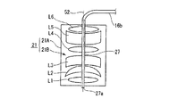
対物光学系20は、図4に示すように、レンズ鏡筒20Aに、基板11側(図4の下側)からレンズL1〜L6が順次配列されてなる対物レンズ20Bが収められたものである。対物光学系20の光軸51は、上記実施形態の欠陥修正装置100において、対物光学系10の光軸50に対応する位置に配置される。
吐出部26は、レンズ鏡筒20Aの側面を光軸50に沿って延ばされたストレート部26c、ストレート部26cからレンズ鏡筒20Aの基板11側の端部を径方向内側に横切る横断部26b、および横断部26bの先端から光軸51に沿って基板11側に向かって延ばされた吐出ノズル26aによって構成される略Z字状のガラス管などの管状部材である。ストレート部26cは、このような位置関係を保持するように、レンズ鏡筒20Aの側部に対して固定されており、ストレート部26cの基板11と反対側の端部は、上記実施形態の材料供給管16bと接続されている。
吐出機構は、特に図示しないが、上記実施形態の吐出機構16dと同様のものが、吐出部26の材料供給管16bとの接続部、または材料供給管16bの管路上に設けられている。
As shown in FIG. 4, the objective
The
Although the discharge mechanism is not particularly illustrated, the same discharge mechanism as the
このような構成によれば、吐出ノズル26aは、観察光学系で観察像を形成する光の光路の最外径の範囲内において、対物光学系の被検体側の外部に固定して設けられており、上記実施形態と同様に、観察される視野範囲内の一定位置から、被検体の表面に向けて修正材料を確実に吐出することができる。
本変形例では、吐出ノズル26aと、横断部26bとによって、対物レンズ20Bを透過する光束が遮蔽されるが、吐出部26の管径をできるだけ細くし、横断部26cをレンズL1側にできるだけ近づけることで、光束が遮蔽されることによる光量低下を必要に応じて低減することができる。
According to such a configuration, the
In this modification, the light beam transmitted through the
次に、本発明の実施形態の第2変形例について説明する。
図5は、本発明の実施形態の第2変形例の対物光学系の近傍の様子を模式的に示す断面図である。
Next, a second modification of the embodiment of the present invention will be described.
FIG. 5 is a cross-sectional view schematically showing the vicinity of the objective optical system of the second modification of the embodiment of the present invention.
本変形例は、上記第1の実施形態の欠陥修正装置100の対物光学系10、吐出部16に代えて、それぞれ図5に示す対物光学系21、吐出部27を備えるものである。以下、上記実施形態と異なる点を中心に説明する。
In this modification, instead of the objective
対物光学系21は、図5に示すように、レンズ鏡筒21Aに、基板11側(図5の下側)からレンズL1〜L6が順次配列されてなる対物レンズ21Bが収められたものである。レンズL1〜L6は、対物レンズ20Bと同様のレンズ構成を採用することができるが、各レンズの中心に貫通孔が設けられている。
対物光学系20の光軸52は、上記実施形態の欠陥修正装置100において、対物光学系10の光軸50に対応する位置に配置される。
吐出部27は、対物レンズ21Bの中心に設けられた貫通孔を光軸52に沿って貫通して、対物レンズ21Bに固定されたガラス管などの管状部材であり、最も基板11側のレンズL1の近傍の外部側に突出する先端に吐出ノズル27aが形成されている。
吐出機構は、特に図示しないが、上記実施形態の吐出機構16dと同様のものが、吐出部26の材料供給管16bとの接続部、または材料供給管16bの管路上に設けられている。
As shown in FIG. 5, the objective
The
The
Although the discharge mechanism is not particularly illustrated, the same discharge mechanism as the
本変形例は、光束の遮蔽部が、対物レンズ21Bの基板11と反対側の端部において、光路を横断する材料供給管16bとなっている点が上記第1変形例と異なる例となっている。
この場合、第1変形例に比べて、光量低下量は略同じであるが、遮蔽部が像面から十分離れた略平行光束の光路に設けられるため、観察画像に対する画質劣化の影響をより低減することができる。
This modification is an example different from the first modification in that the light shielding portion is a
In this case, the amount of light reduction is substantially the same as in the first modified example, but the influence of image quality deterioration on the observed image is further reduced because the shielding portion is provided in the optical path of a substantially parallel light beam sufficiently separated from the image plane. can do.
なお、上記の説明では、被検体が水平に載置され、対物光学系の光軸が鉛直軸に沿って配置された場合の例で説明したが、修正材料の着弾位置精度が許容できる場合には、それぞれの水平面、鉛直軸から傾斜させた配置としてもよい。 In the above description, the example in which the subject is placed horizontally and the optical axis of the objective optical system is arranged along the vertical axis has been described. However, when the landing position accuracy of the correction material is acceptable. May be arranged so as to be inclined from the respective horizontal planes and the vertical axis.
また、上記の説明では、レーザ照射光学系においてビーム整形する手段として、DMDからなる空間変調素子6を用いたが、DMD以外の空間変調素子を用いてもよい。
また、レーザ光の光路上に可変スリットを配置して開口制限を行って照射範囲を調整し、この照射範囲を被検体に対して相対移動させる構成としてもよい。
また、スキャニングに要する時間が許容できる場合には、ガルバノミラーのような偏向器を用い、レーザの投射位置を可変する構成としてもよい。
In the above description, the spatial modulation element 6 made of DMD is used as means for beam shaping in the laser irradiation optical system. However, a spatial modulation element other than DMD may be used.
Alternatively, a variable slit may be arranged on the optical path of the laser beam to limit the opening to adjust the irradiation range, and the irradiation range may be moved relative to the subject.
If the time required for scanning is acceptable, a deflector such as a galvanometer mirror may be used to vary the laser projection position.
また、上記の説明では、吐出ノズルが対物光学系の光軸近傍に設けられた場合の例で説明したが、吐出ノズルは、被検体と対物光学系との相対位置関係が固定され、観察光学系で観察像を形成する光の光路の最外径の範囲内であれば、観察光学系の視野範囲内の一定位置に吐出ノズルを位置させることができるので、配置位置は光軸の近傍には限定されない。
例えば、上記実施形態の場合、吐出ノズルは、図3に示す凸面反射鏡10Aの裏面10dと光線Q1に囲まれた三角錐の領域内の場合、どの位置でも問題なく配置することができる。
また、観察光学系の視野範囲の直上の領域に配置することも着弾精度を高精度にする点では有効である。
In the above description, the example in which the discharge nozzle is provided in the vicinity of the optical axis of the objective optical system has been described. However, the relative positional relationship between the subject and the objective optical system is fixed in the discharge nozzle, and the observation optical Since the discharge nozzle can be positioned at a fixed position within the visual field range of the observation optical system as long as it is within the outermost diameter of the optical path of the light that forms the observation image in the system, the arrangement position is close to the optical axis. Is not limited.
For example, in the above embodiment, the discharge nozzle, when the
In addition, it is also effective to arrange it in a region immediately above the visual field range of the observation optical system in order to increase the landing accuracy.
また、上記の説明では、吐出ノズルが対物光学系の被検体側の外部に設けられた場合の例で説明したが、修正材料の吐出に支障がなければ、吐出ノズルは対物光学系の内部に設けられていてもよい。例えば、図3において、吐出ノズル16aの先端が、凸面反射鏡10Aの裏面10dと同一面またはより内部側に配置されていてもよい。
In the above description, the example in which the discharge nozzle is provided outside the object side of the objective optical system has been described. However, if there is no problem in discharging the correction material, the discharge nozzle is placed inside the objective optical system. It may be provided. For example, in FIG. 3, the tip of the
また、上記の説明では、光路分岐素子を修正材料吐出部に貫通させた構成の例で説明したが、光路分岐素子は、対物光学系等を固定する適宜の筐体などによって保持することにより、修正材料吐出部に貫通させない構成としてもよい。 In the above description, the example of the configuration in which the optical path branching element is passed through the correction material discharge unit has been described, but the optical path branching element is held by an appropriate casing or the like that fixes the objective optical system, etc. It is good also as a structure which does not penetrate the correction material discharge part.
また、上記の説明では、レーザ光源から出射されるレーザ光の光量を均一化するために、光ファイバ3を透過させる構成の例で説明したが、レーザ光の均一化手段は、他の光学素子、例えば、フライアイレンズ、回折素子、非球面レンズや、カレイド型ロッドを用いたものなどの種々の構成のホモジナイザーなどを用いた構成としてもよい。 In the above description, in order to make the light quantity of the laser light emitted from the laser light source uniform, the example of the configuration that transmits the optical fiber 3 has been described. However, the means for making the laser light uniform includes other optical elements. For example, a configuration using a homogenizer having various configurations such as a fly-eye lens, a diffractive element, an aspheric lens, and a kaleido type rod may be used.
また、上記の各実施形態、各変形例に記載された構成要素は、技術的に可能であれば、本発明の技術的思想の範囲内で適宜組み合わせて実施することができる。 In addition, the constituent elements described in the above embodiments and modifications can be implemented in appropriate combination within the scope of the technical idea of the present invention, if technically possible.
次に、上記に説明した実施形態の対物光学系の実施例である数値実施例について説明する。
図6は、本発明の実施形態の対物光学系の数値実施例の光路図である。ここで、図中の光線は、FAN光線(光束中の光線)を示している。
Next, numerical examples that are examples of the objective optical system according to the embodiment described above will be described.
FIG. 6 is an optical path diagram of a numerical example of the objective optical system according to the embodiment of the present invention. Here, the light beam in the figure indicates a FAN light beam (a light beam in the light beam).
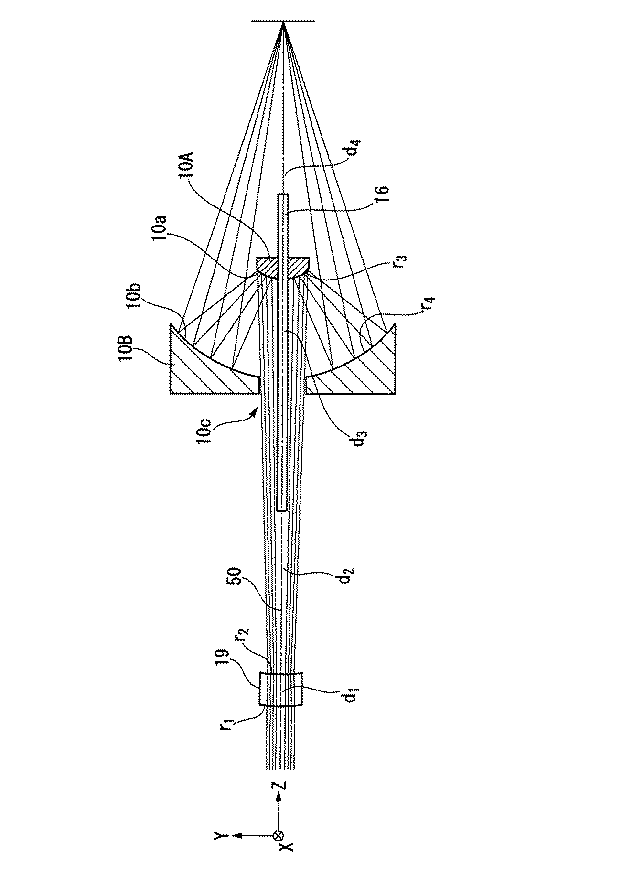
本実施例は、対物光学系10の物体側に、負のメニスカスレンズからなるレンズ19を配置することにより、対物光学系10と合わせて無限遠設計の対物光学系を構成しているものである。
In this embodiment, an objective optical system having an infinity design is configured together with the objective
下記に数値実施例の、光学系の構成パラメータを示す。図6に表記されたri、di(iは整数)は、下記に示す光学系の構成パラメータのri、diに対応する。また屈折率については、d線(波長587.56nm)に対するものを表記している。
座標系は、光線追跡において、軸上主光線に沿う方向をZ軸方向とし、物体側からレンズ19に向かう方向をZ軸正方向とし、紙面をY−Z平面とし、紙面の表から裏へ向かう方向をX軸正方向とし、X軸、Z軸と右手直交座標系を構成する軸をY軸とする。
本実施例に用いる非球面の形状は、このXYZ直交座標系を用いて、以下の定義式(a)で与えられる回転対称非球面である。なお、下記数値実施例のレンズデータは、逆光線追跡のデータとなっているので、図6の左側の−Zの方向が像側であり、右側の集光点が物体面の位置となる。
The configuration parameters of the optical system in the numerical examples are shown below. R i and d i (i is an integer) shown in FIG. 6 correspond to the configuration parameters r i and d i of the optical system shown below. The refractive index is shown for d-line (wavelength 587.56 nm).
In the ray tracing, the direction along the axial principal ray is the Z-axis direction, the direction from the object side toward the
The shape of the aspherical surface used in the present embodiment is a rotationally symmetric aspherical surface given by the following definition formula (a) using this XYZ orthogonal coordinate system. Since the lens data in the following numerical examples is data of reverse ray tracing, the direction of −Z on the left side of FIG. 6 is the image side, and the light collecting point on the right side is the position of the object plane.
ここで、h=√(X2 +Y2 )であり、cは頂点の近軸曲率半径、kはコーニック定数(円錐定数)、A、B、C、…はそれぞれ4次、6次、8次、…の非球面係数である。この定義式(a)のZ軸が回転対称非球面の軸となる。
以下に示す構成パラメータにおいて、長さの単位は(mm)である。
また、データの記載されていない非球面に関する項は0である。
Here, h = √ (X 2 + Y 2 ), c is the paraxial radius of curvature of the apex, k is the conic constant (conical constant), A, B, C,... Are 4th order, 6th order, 8th order, respectively. Are aspheric coefficients of. The Z axis of the definition formula (a) is the axis of the rotationally symmetric aspheric surface.
In the configuration parameters shown below, the unit of length is (mm).
The term relating to the aspherical surface for which no data is described is zero.
面番号 曲率半径 面間隔 屈折率 アッベ数
物体面 ∞ ∞
1 r1 = 13.77 d1 = 35.00 n1 = 1.7847 ν1 = 25.7
2 r2 = 8.88 d2 = 25.00
3 非球面[1] d3 = -5.73
4 非球面[2] (絞り) d4 = 21.66
像 面 ∞ d5 = 0.00
非球面[1]
c 2.95
k -2.0921
A 2.1388x10⁻³ B -3.2970x10⁻⁴
非球面[2]
c 10.78
k -6.5828x10⁻¹
A 3.5722x10⁻⁵ B 1.7793x10⁻⁷
焦点距離 f =2.7627mm
NA=0.33
ミラー面(凸面鏡)から試料面までの距離 15.9mm
倍率 65倍(結像レンズの焦点距離 180mm)
Surface number Curvature radius Surface spacing Refractive index Abbe number Object surface ∞ ∞
1 r 1 = 13.77 d 1 = 35.00 n 1 = 1.7847 ν 1 = 25.7
2 r 2 = 8.88 d 2 = 25.00
3 Aspherical surface [1] d 3 = -5.73
4 Aspherical surface [2] (Aperture) d 4 = 21.66
Image plane ∞ d 5 = 0.00
Aspherical [1]
c 2.95
k -2.0921
A 2.1388x10 -3 B -3.2970x10 -4
Aspherical [2]
c 10.78
k -6.5828x10 -1
A 3.5722x10 -5 B 1.7793x10 -7
Focal length f = 2.7627mm
NA = 0.33
Distance from mirror surface (convex mirror) to sample surface 15.9mm
Magnification 65 times (focal length of imaging lens 180mm)
6 空間変調素子
7、12 結像レンズ
9 ハーフミラー(光路分岐素子)
10、20、21 対物光学系
10A 凸面反射鏡
10B 凹面反射鏡
10a 凸反射面
10b 凹反射面
10c 開口部
11 基板(被検体)
13 撮像素子
14 照明ランプ
16、26、27 吐出部(修正材料吐出部)
16a、26a、27a 吐出ノズル
19 レンズ
20B、21B 対物レンズ
30 レーザ光源
31a、31b レーザ光
32 オン光
100 欠陥修正装置
6
10, 20, 21 Objective
13
16a, 26a,
Claims (5)
前記被検体の表面に形成されたパターンの欠陥を修正する修正材料を前記被検体の表面に吐出する吐出ノズルを有する修正材料吐出部と、
ビーム整形されたレーザ光を前記被検体の表面に照射するレーザ照射光学系とを備え、 前記観察光学系および前記レーザ照射光学系が、前記被検体側に共通の対物光学系を有し、
前記修正材料吐出部の前記吐出ノズルが、前記観察光学系で観察像を形成する光の光路の最外径の範囲内において、前記対物光学系の内部に固定して設けられ、
前記対物光学系の、前記被検体とは反対側の光路中に、被検体側から前記観察光学系に向かう光を反射する光路分岐素子が設けられ、
前記修正材料吐出部は、前記対物光学系の光軸上および前記光路分岐素子の中心部に貫通されるとともに前記対物光学系および前記光路分岐素子に固定され、前記光路分岐素子の支持部材を兼用していることを特徴とする欠陥修正装置。 An observation optical system for magnifying and observing a pattern formed on the surface of the subject;
A correction material discharge unit having a discharge nozzle for discharging a correction material for correcting a defect in a pattern formed on the surface of the subject to the surface of the subject;
A laser irradiation optical system that irradiates the surface of the subject with laser light that has undergone beam shaping, and the observation optical system and the laser irradiation optical system have a common objective optical system on the subject side,
The discharge nozzle of the modifying material discharge portion is in the range of the outermost diameter of the optical path of light forming the observation image in the observation optical system fixedly mounted on the inner portion of the objective optical system,
In the optical path of the objective optical system opposite to the subject, an optical path branching element that reflects light traveling from the subject side toward the observation optical system is provided,
The correction material discharge unit penetrates the optical axis of the objective optical system and the center of the optical path branching element and is fixed to the objective optical system and the optical path branching element, and also serves as a support member for the optical path branching element A defect correcting device characterized by that.
Priority Applications (1)
| Application Number | Priority Date | Filing Date | Title |
|---|---|---|---|
| JP2007002277A JP5057787B2 (en) | 2007-01-10 | 2007-01-10 | Defect correction device |
Applications Claiming Priority (1)
| Application Number | Priority Date | Filing Date | Title |
|---|---|---|---|
| JP2007002277A JP5057787B2 (en) | 2007-01-10 | 2007-01-10 | Defect correction device |
Publications (2)
| Publication Number | Publication Date |
|---|---|
| JP2008170605A JP2008170605A (en) | 2008-07-24 |
| JP5057787B2 true JP5057787B2 (en) | 2012-10-24 |
Family
ID=39698768
Family Applications (1)
| Application Number | Title | Priority Date | Filing Date |
|---|---|---|---|
| JP2007002277A Expired - Fee Related JP5057787B2 (en) | 2007-01-10 | 2007-01-10 | Defect correction device |
Country Status (1)
| Country | Link |
|---|---|
| JP (1) | JP5057787B2 (en) |
Families Citing this family (2)
| Publication number | Priority date | Publication date | Assignee | Title |
|---|---|---|---|---|
| WO2012140689A1 (en) * | 2011-04-11 | 2012-10-18 | エンジニアリングシステム株式会社 | Liquid discharging device with optical system for observation |
| JP6510768B2 (en) * | 2014-05-23 | 2019-05-08 | 株式会社オーク製作所 | Exposure device |
Family Cites Families (11)
| Publication number | Priority date | Publication date | Assignee | Title |
|---|---|---|---|---|
| JPS6047564B2 (en) * | 1979-01-19 | 1985-10-22 | オリンパス光学工業株式会社 | Micromanipulator |
| DE3854620T2 (en) * | 1987-08-12 | 1996-03-28 | Olympus Optical Co | TUNNEL SCAN MICROSCOPE. |
| US4863253A (en) * | 1987-09-25 | 1989-09-05 | Spectra-Tech, Inc. | High magnification reflecting microscope objective having a dual magnification mode and zoom magnification capability |
| JPH04307314A (en) * | 1991-04-04 | 1992-10-29 | Hitachi Ltd | Photographing apparatus of mounting pattern or electronic components in mounting machine |
| JPH0540034A (en) * | 1991-08-08 | 1993-02-19 | Nikon Corp | Compound microscope |
| JPH0735856A (en) * | 1993-05-18 | 1995-02-07 | Opt:Kk | Optical range finder |
| JPH07194557A (en) * | 1994-10-03 | 1995-08-01 | Canon Inc | Ophthalmic system |
| JPH09138117A (en) * | 1995-11-14 | 1997-05-27 | Dainippon Screen Mfg Co Ltd | Optical measuring apparatus |
| JP4542380B2 (en) * | 2004-06-29 | 2010-09-15 | 株式会社ブイ・テクノロジー | Pattern correction device |
| JP2006130460A (en) * | 2004-11-09 | 2006-05-25 | Ntn Corp | Device for correcting fine pattern |
| WO2006100780A1 (en) * | 2005-03-24 | 2006-09-28 | Olympus Corporation | Repairing method and apparatus therefor |
-
2007
- 2007-01-10 JP JP2007002277A patent/JP5057787B2/en not_active Expired - Fee Related
Also Published As
| Publication number | Publication date |
|---|---|
| JP2008170605A (en) | 2008-07-24 |
Similar Documents
| Publication | Publication Date | Title |
|---|---|---|
| JP5185617B2 (en) | Repair method and apparatus | |
| JP5137488B2 (en) | Laser irradiation apparatus and laser processing system using the same | |
| JP3996135B2 (en) | Lithographic apparatus and device manufacturing method | |
| JP2021076853A (en) | Optical system and method of correcting mask defects using the same | |
| JP2018533769A (en) | Wide-field high-resolution microscope | |
| JP2010032542A (en) | X-RAY MICROSCOPE OF REFLECTOR TYPE AND INSPECTION SYSTEM WHICH INSPECT OBJECT ON WAVELENGTH <=100 nm | |
| JP4955425B2 (en) | Laser processing equipment | |
| JP2002351055A (en) | Defect correcting method of photomask | |
| US20180275528A1 (en) | Optical system for producing lithographic structures | |
| JP2007326132A (en) | Laser beam machining apparatus | |
| JP4879619B2 (en) | Laser processing equipment | |
| KR101939876B1 (en) | Raser repair device | |
| JP5057787B2 (en) | Defect correction device | |
| CN203380507U (en) | Laser processing device | |
| JP5689952B2 (en) | Liquid ejection device with optical system for observation | |
| JP2007029959A (en) | Laser beam machining apparatus | |
| JP2014083562A (en) | Laser irradiation unit, and laser processing apparatus | |
| JP2014529734A (en) | Inspection / repair / inspection system | |
| TW202235195A (en) | Observation device and observation method performing the moving of the condensing position at high speed even if imaging region is larger | |
| JP5196778B2 (en) | Irradiation optical system and irradiation apparatus | |
| JP2006326629A (en) | Laser beam machining apparatus and its machining method | |
| US20220373778A1 (en) | Illumination arrangement for a microscope, microscope and method for illuminating a sample volume in a microscope | |
| JP2007042858A (en) | Projection aligner | |
| JP4961541B2 (en) | Defect correction method and apparatus | |
| TW202009081A (en) | Laser processing apparatus |
Legal Events
| Date | Code | Title | Description |
|---|---|---|---|
| A621 | Written request for application examination |
Free format text: JAPANESE INTERMEDIATE CODE: A621 Effective date: 20091228 |
|
| A131 | Notification of reasons for refusal |
Free format text: JAPANESE INTERMEDIATE CODE: A131 Effective date: 20111101 |
|
| A521 | Written amendment |
Free format text: JAPANESE INTERMEDIATE CODE: A821 Effective date: 20111228 Free format text: JAPANESE INTERMEDIATE CODE: A523 Effective date: 20111228 |
|
| A131 | Notification of reasons for refusal |
Free format text: JAPANESE INTERMEDIATE CODE: A131 Effective date: 20120214 |
|
| A521 | Written amendment |
Free format text: JAPANESE INTERMEDIATE CODE: A523 Effective date: 20120405 Free format text: JAPANESE INTERMEDIATE CODE: A821 Effective date: 20120405 |
|
| TRDD | Decision of grant or rejection written | ||
| A01 | Written decision to grant a patent or to grant a registration (utility model) |
Free format text: JAPANESE INTERMEDIATE CODE: A01 Effective date: 20120717 |
|
| A01 | Written decision to grant a patent or to grant a registration (utility model) |
Free format text: JAPANESE INTERMEDIATE CODE: A01 |
|
| A61 | First payment of annual fees (during grant procedure) |
Free format text: JAPANESE INTERMEDIATE CODE: A61 Effective date: 20120731 |
|
| FPAY | Renewal fee payment (event date is renewal date of database) |
Free format text: PAYMENT UNTIL: 20150810 Year of fee payment: 3 |
|
| FPAY | Renewal fee payment (event date is renewal date of database) |
Free format text: PAYMENT UNTIL: 20150810 Year of fee payment: 3 |
|
| LAPS | Cancellation because of no payment of annual fees |