JP5057778B2 - Semiconductor sensor element and manufacturing method made of group III nitride semiconductor, and measuring method using the semiconductor sensor element - Google Patents
Semiconductor sensor element and manufacturing method made of group III nitride semiconductor, and measuring method using the semiconductor sensor element Download PDFInfo
- Publication number
- JP5057778B2 JP5057778B2 JP2006504725A JP2006504725A JP5057778B2 JP 5057778 B2 JP5057778 B2 JP 5057778B2 JP 2006504725 A JP2006504725 A JP 2006504725A JP 2006504725 A JP2006504725 A JP 2006504725A JP 5057778 B2 JP5057778 B2 JP 5057778B2
- Authority
- JP
- Japan
- Prior art keywords
- semiconductor
- sensor element
- semiconductor layer
- region
- homogeneous
- Prior art date
- Legal status (The legal status is an assumption and is not a legal conclusion. Google has not performed a legal analysis and makes no representation as to the accuracy of the status listed.)
- Expired - Fee Related
Links
- 239000004065 semiconductor Substances 0.000 title claims description 283
- 238000000034 method Methods 0.000 title claims description 28
- 150000004767 nitrides Chemical class 0.000 title claims description 17
- 238000004519 manufacturing process Methods 0.000 title claims description 13
- 239000000758 substrate Substances 0.000 claims description 138
- 229910002601 GaN Inorganic materials 0.000 claims description 63
- JMASRVWKEDWRBT-UHFFFAOYSA-N Gallium nitride Chemical compound [Ga]#N JMASRVWKEDWRBT-UHFFFAOYSA-N 0.000 claims description 44
- 239000000463 material Substances 0.000 claims description 37
- 230000001133 acceleration Effects 0.000 claims description 33
- 238000005530 etching Methods 0.000 claims description 32
- XUIMIQQOPSSXEZ-UHFFFAOYSA-N Silicon Chemical compound [Si] XUIMIQQOPSSXEZ-UHFFFAOYSA-N 0.000 claims description 27
- 230000008859 change Effects 0.000 claims description 27
- 239000010703 silicon Substances 0.000 claims description 27
- 229910052710 silicon Inorganic materials 0.000 claims description 27
- 230000007704 transition Effects 0.000 claims description 19
- RNQKDQAVIXDKAG-UHFFFAOYSA-N aluminum gallium Chemical compound [Al].[Ga] RNQKDQAVIXDKAG-UHFFFAOYSA-N 0.000 claims description 18
- 239000002800 charge carrier Substances 0.000 claims description 13
- 238000001465 metallisation Methods 0.000 claims description 11
- 229910052757 nitrogen Inorganic materials 0.000 claims description 9
- 238000000926 separation method Methods 0.000 claims description 8
- 239000007789 gas Substances 0.000 claims description 7
- PXHVJJICTQNCMI-UHFFFAOYSA-N Nickel Chemical compound [Ni] PXHVJJICTQNCMI-UHFFFAOYSA-N 0.000 claims description 6
- 238000001312 dry etching Methods 0.000 claims description 5
- 229910052738 indium Inorganic materials 0.000 claims description 5
- 238000001020 plasma etching Methods 0.000 claims description 5
- 229910052782 aluminium Inorganic materials 0.000 claims description 4
- XAGFODPZIPBFFR-UHFFFAOYSA-N aluminium Chemical compound [Al] XAGFODPZIPBFFR-UHFFFAOYSA-N 0.000 claims description 4
- OKTJSMMVPCPJKN-UHFFFAOYSA-N Carbon Chemical compound [C] OKTJSMMVPCPJKN-UHFFFAOYSA-N 0.000 claims description 3
- 229910052799 carbon Inorganic materials 0.000 claims description 3
- 229910003460 diamond Inorganic materials 0.000 claims description 3
- 239000010432 diamond Substances 0.000 claims description 3
- 239000000945 filler Substances 0.000 claims description 3
- PCHJSUWPFVWCPO-UHFFFAOYSA-N gold Chemical compound [Au] PCHJSUWPFVWCPO-UHFFFAOYSA-N 0.000 claims description 3
- 229910052737 gold Inorganic materials 0.000 claims description 3
- 239000010931 gold Substances 0.000 claims description 3
- 229910052736 halogen Inorganic materials 0.000 claims description 3
- 150000002367 halogens Chemical class 0.000 claims description 3
- 239000011777 magnesium Substances 0.000 claims description 3
- 229910052759 nickel Inorganic materials 0.000 claims description 3
- 239000000126 substance Substances 0.000 claims description 3
- 229910018072 Al 2 O 3 Inorganic materials 0.000 claims description 2
- FYYHWMGAXLPEAU-UHFFFAOYSA-N Magnesium Chemical compound [Mg] FYYHWMGAXLPEAU-UHFFFAOYSA-N 0.000 claims description 2
- RTAQQCXQSZGOHL-UHFFFAOYSA-N Titanium Chemical compound [Ti] RTAQQCXQSZGOHL-UHFFFAOYSA-N 0.000 claims description 2
- 229910052731 fluorine Inorganic materials 0.000 claims description 2
- 239000011737 fluorine Substances 0.000 claims description 2
- 229910052749 magnesium Inorganic materials 0.000 claims description 2
- 239000012495 reaction gas Substances 0.000 claims description 2
- 239000010936 titanium Substances 0.000 claims description 2
- 229910052719 titanium Inorganic materials 0.000 claims description 2
- 150000001875 compounds Chemical class 0.000 claims 7
- 230000000873 masking effect Effects 0.000 claims 3
- 238000000691 measurement method Methods 0.000 claims 3
- 229910052755 nonmetal Inorganic materials 0.000 claims 3
- ZAMOUSCENKQFHK-UHFFFAOYSA-N Chlorine atom Chemical compound [Cl] ZAMOUSCENKQFHK-UHFFFAOYSA-N 0.000 claims 1
- PXGOKWXKJXAPGV-UHFFFAOYSA-N Fluorine Chemical compound FF PXGOKWXKJXAPGV-UHFFFAOYSA-N 0.000 claims 1
- 244000126211 Hericium coralloides Species 0.000 claims 1
- 229910004298 SiO 2 Inorganic materials 0.000 claims 1
- 239000000654 additive Substances 0.000 claims 1
- 230000000996 additive effect Effects 0.000 claims 1
- 229910052801 chlorine Inorganic materials 0.000 claims 1
- 239000000460 chlorine Substances 0.000 claims 1
- 239000007787 solid Substances 0.000 claims 1
- 239000012528 membrane Substances 0.000 description 18
- 230000000694 effects Effects 0.000 description 13
- 239000000872 buffer Substances 0.000 description 11
- 238000005452 bending Methods 0.000 description 8
- 238000005259 measurement Methods 0.000 description 8
- 230000010287 polarization Effects 0.000 description 6
- 239000012535 impurity Substances 0.000 description 4
- NWAIGJYBQQYSPW-UHFFFAOYSA-N azanylidyneindigane Chemical compound [In]#N NWAIGJYBQQYSPW-UHFFFAOYSA-N 0.000 description 3
- 230000008901 benefit Effects 0.000 description 3
- PMHQVHHXPFUNSP-UHFFFAOYSA-M copper(1+);methylsulfanylmethane;bromide Chemical compound Br[Cu].CSC PMHQVHHXPFUNSP-UHFFFAOYSA-M 0.000 description 3
- 230000001419 dependent effect Effects 0.000 description 3
- -1 diamond) Chemical compound 0.000 description 3
- 238000001000 micrograph Methods 0.000 description 3
- 230000005355 Hall effect Effects 0.000 description 2
- VYPSYNLAJGMNEJ-UHFFFAOYSA-N Silicium dioxide Chemical compound O=[Si]=O VYPSYNLAJGMNEJ-UHFFFAOYSA-N 0.000 description 2
- 230000003321 amplification Effects 0.000 description 2
- QVGXLLKOCUKJST-UHFFFAOYSA-N atomic oxygen Chemical compound [O] QVGXLLKOCUKJST-UHFFFAOYSA-N 0.000 description 2
- 238000005516 engineering process Methods 0.000 description 2
- 229910052751 metal Inorganic materials 0.000 description 2
- 239000002184 metal Substances 0.000 description 2
- 238000003199 nucleic acid amplification method Methods 0.000 description 2
- 229910052760 oxygen Inorganic materials 0.000 description 2
- 239000001301 oxygen Substances 0.000 description 2
- 230000008569 process Effects 0.000 description 2
- 238000010561 standard procedure Methods 0.000 description 2
- RZVAJINKPMORJF-UHFFFAOYSA-N Acetaminophen Chemical compound CC(=O)NC1=CC=C(O)C=C1 RZVAJINKPMORJF-UHFFFAOYSA-N 0.000 description 1
- 229910002704 AlGaN Inorganic materials 0.000 description 1
- 238000009623 Bosch process Methods 0.000 description 1
- BQCADISMDOOEFD-UHFFFAOYSA-N Silver Chemical compound [Ag] BQCADISMDOOEFD-UHFFFAOYSA-N 0.000 description 1
- 229910020776 SixNy Inorganic materials 0.000 description 1
- 238000009825 accumulation Methods 0.000 description 1
- 230000009471 action Effects 0.000 description 1
- 238000005275 alloying Methods 0.000 description 1
- 239000013590 bulk material Substances 0.000 description 1
- 238000003486 chemical etching Methods 0.000 description 1
- 229910052681 coesite Inorganic materials 0.000 description 1
- 239000002131 composite material Substances 0.000 description 1
- 230000006835 compression Effects 0.000 description 1
- 238000007906 compression Methods 0.000 description 1
- 238000012937 correction Methods 0.000 description 1
- 229910052906 cristobalite Inorganic materials 0.000 description 1
- 239000013078 crystal Substances 0.000 description 1
- 230000001186 cumulative effect Effects 0.000 description 1
- 239000012530 fluid Substances 0.000 description 1
- APFVFJFRJDLVQX-UHFFFAOYSA-N indium atom Chemical compound [In] APFVFJFRJDLVQX-UHFFFAOYSA-N 0.000 description 1
- 150000002500 ions Chemical class 0.000 description 1
- 230000007246 mechanism Effects 0.000 description 1
- JHJNPOSPVGRIAN-SFHVURJKSA-N n-[3-[(1s)-1-[[6-(3,4-dimethoxyphenyl)pyrazin-2-yl]amino]ethyl]phenyl]-5-methylpyridine-3-carboxamide Chemical compound C1=C(OC)C(OC)=CC=C1C1=CN=CC(N[C@@H](C)C=2C=C(NC(=O)C=3C=C(C)C=NC=3)C=CC=2)=N1 JHJNPOSPVGRIAN-SFHVURJKSA-N 0.000 description 1
- 238000005121 nitriding Methods 0.000 description 1
- 230000003071 parasitic effect Effects 0.000 description 1
- 230000000737 periodic effect Effects 0.000 description 1
- 238000010079 rubber tapping Methods 0.000 description 1
- 230000035945 sensitivity Effects 0.000 description 1
- 239000000377 silicon dioxide Substances 0.000 description 1
- 235000012239 silicon dioxide Nutrition 0.000 description 1
- 229910052709 silver Inorganic materials 0.000 description 1
- 239000004332 silver Substances 0.000 description 1
- 230000003068 static effect Effects 0.000 description 1
- 229910052682 stishovite Inorganic materials 0.000 description 1
- 238000012360 testing method Methods 0.000 description 1
- 229910052905 tridymite Inorganic materials 0.000 description 1
Images


Classifications
-
- G—PHYSICS
- G01—MEASURING; TESTING
- G01L—MEASURING FORCE, STRESS, TORQUE, WORK, MECHANICAL POWER, MECHANICAL EFFICIENCY, OR FLUID PRESSURE
- G01L9/00—Measuring steady of quasi-steady pressure of fluid or fluent solid material by electric or magnetic pressure-sensitive elements; Transmitting or indicating the displacement of mechanical pressure-sensitive elements, used to measure the steady or quasi-steady pressure of a fluid or fluent solid material, by electric or magnetic means
- G01L9/0041—Transmitting or indicating the displacement of flexible diaphragms
- G01L9/0051—Transmitting or indicating the displacement of flexible diaphragms using variations in ohmic resistance
- G01L9/0052—Transmitting or indicating the displacement of flexible diaphragms using variations in ohmic resistance of piezoresistive elements
- G01L9/0055—Transmitting or indicating the displacement of flexible diaphragms using variations in ohmic resistance of piezoresistive elements bonded on a diaphragm
-
- B—PERFORMING OPERATIONS; TRANSPORTING
- B81—MICROSTRUCTURAL TECHNOLOGY
- B81C—PROCESSES OR APPARATUS SPECIALLY ADAPTED FOR THE MANUFACTURE OR TREATMENT OF MICROSTRUCTURAL DEVICES OR SYSTEMS
- B81C1/00—Manufacture or treatment of devices or systems in or on a substrate
- B81C1/00015—Manufacture or treatment of devices or systems in or on a substrate for manufacturing microsystems
- B81C1/00134—Manufacture or treatment of devices or systems in or on a substrate for manufacturing microsystems comprising flexible or deformable structures
- B81C1/00142—Bridges
-
- G—PHYSICS
- G01—MEASURING; TESTING
- G01L—MEASURING FORCE, STRESS, TORQUE, WORK, MECHANICAL POWER, MECHANICAL EFFICIENCY, OR FLUID PRESSURE
- G01L1/00—Measuring force or stress, in general
- G01L1/20—Measuring force or stress, in general by measuring variations in ohmic resistance of solid materials or of electrically-conductive fluids; by making use of electrokinetic cells, i.e. liquid-containing cells wherein an electrical potential is produced or varied upon the application of stress
- G01L1/22—Measuring force or stress, in general by measuring variations in ohmic resistance of solid materials or of electrically-conductive fluids; by making use of electrokinetic cells, i.e. liquid-containing cells wherein an electrical potential is produced or varied upon the application of stress using resistance strain gauges
- G01L1/2287—Measuring force or stress, in general by measuring variations in ohmic resistance of solid materials or of electrically-conductive fluids; by making use of electrokinetic cells, i.e. liquid-containing cells wherein an electrical potential is produced or varied upon the application of stress using resistance strain gauges constructional details of the strain gauges
- G01L1/2293—Measuring force or stress, in general by measuring variations in ohmic resistance of solid materials or of electrically-conductive fluids; by making use of electrokinetic cells, i.e. liquid-containing cells wherein an electrical potential is produced or varied upon the application of stress using resistance strain gauges constructional details of the strain gauges of the semi-conductor type
-
- G—PHYSICS
- G01—MEASURING; TESTING
- G01P—MEASURING LINEAR OR ANGULAR SPEED, ACCELERATION, DECELERATION, OR SHOCK; INDICATING PRESENCE, ABSENCE, OR DIRECTION, OF MOVEMENT
- G01P15/00—Measuring acceleration; Measuring deceleration; Measuring shock, i.e. sudden change of acceleration
- G01P15/02—Measuring acceleration; Measuring deceleration; Measuring shock, i.e. sudden change of acceleration by making use of inertia forces using solid seismic masses
- G01P15/08—Measuring acceleration; Measuring deceleration; Measuring shock, i.e. sudden change of acceleration by making use of inertia forces using solid seismic masses with conversion into electric or magnetic values
- G01P15/09—Measuring acceleration; Measuring deceleration; Measuring shock, i.e. sudden change of acceleration by making use of inertia forces using solid seismic masses with conversion into electric or magnetic values by piezoelectric pick-up
- G01P15/0922—Measuring acceleration; Measuring deceleration; Measuring shock, i.e. sudden change of acceleration by making use of inertia forces using solid seismic masses with conversion into electric or magnetic values by piezoelectric pick-up of the bending or flexing mode type
-
- G—PHYSICS
- G01—MEASURING; TESTING
- G01P—MEASURING LINEAR OR ANGULAR SPEED, ACCELERATION, DECELERATION, OR SHOCK; INDICATING PRESENCE, ABSENCE, OR DIRECTION, OF MOVEMENT
- G01P15/00—Measuring acceleration; Measuring deceleration; Measuring shock, i.e. sudden change of acceleration
- G01P15/02—Measuring acceleration; Measuring deceleration; Measuring shock, i.e. sudden change of acceleration by making use of inertia forces using solid seismic masses
- G01P15/08—Measuring acceleration; Measuring deceleration; Measuring shock, i.e. sudden change of acceleration by making use of inertia forces using solid seismic masses with conversion into electric or magnetic values
- G01P15/12—Measuring acceleration; Measuring deceleration; Measuring shock, i.e. sudden change of acceleration by making use of inertia forces using solid seismic masses with conversion into electric or magnetic values by alteration of electrical resistance
-
- H—ELECTRICITY
- H10—SEMICONDUCTOR DEVICES; ELECTRIC SOLID-STATE DEVICES NOT OTHERWISE PROVIDED FOR
- H10N—ELECTRIC SOLID-STATE DEVICES NOT OTHERWISE PROVIDED FOR
- H10N30/00—Piezoelectric or electrostrictive devices
- H10N30/30—Piezoelectric or electrostrictive devices with mechanical input and electrical output, e.g. functioning as generators or sensors
- H10N30/302—Sensors
-
- B—PERFORMING OPERATIONS; TRANSPORTING
- B81—MICROSTRUCTURAL TECHNOLOGY
- B81B—MICROSTRUCTURAL DEVICES OR SYSTEMS, e.g. MICROMECHANICAL DEVICES
- B81B2201/00—Specific applications of microelectromechanical systems
- B81B2201/02—Sensors
- B81B2201/0228—Inertial sensors
- B81B2201/0235—Accelerometers
-
- B—PERFORMING OPERATIONS; TRANSPORTING
- B81—MICROSTRUCTURAL TECHNOLOGY
- B81B—MICROSTRUCTURAL DEVICES OR SYSTEMS, e.g. MICROMECHANICAL DEVICES
- B81B2201/00—Specific applications of microelectromechanical systems
- B81B2201/02—Sensors
- B81B2201/0264—Pressure sensors
-
- B—PERFORMING OPERATIONS; TRANSPORTING
- B81—MICROSTRUCTURAL TECHNOLOGY
- B81B—MICROSTRUCTURAL DEVICES OR SYSTEMS, e.g. MICROMECHANICAL DEVICES
- B81B2203/00—Basic microelectromechanical structures
- B81B2203/01—Suspended structures, i.e. structures allowing a movement
- B81B2203/0109—Bridges
Description
本発明は、III族窒化物(窒化ガリウム、窒化アルミニウム、窒化インジウムなどを含む)半導体構造を有するセンサ素子に関する。物理的変数の変化(音響振動、加速、偏向、または、温度などにおけるガスまたは流体の流れなどの静圧およびまたは動圧における変化)は、半導体構造が、その圧電特性により変化する物理的変数を電気出力変数または対応する出力信号に変換することによって決定される。以下、III族または第III主族元素は、元素周期表のIII族の略語を用いて説明する。 The present invention relates to a sensor element having a group III nitride (including gallium nitride, aluminum nitride, indium nitride, etc.) semiconductor structure. Changes in physical variables (acoustic vibration, acceleration, deflection, or changes in static and / or dynamic pressure, such as gas or fluid flow in temperature, etc.) can cause physical changes in the semiconductor structure due to its piezoelectric properties. It is determined by converting it into an electrical output variable or a corresponding output signal. Hereinafter, Group III or Group III main group elements will be described using Group III abbreviations in the Periodic Table of Elements.
III族窒化物半導体によるマイクロセンサは、すでに公知の技術である。特許文献1(米国特許公報6,066,319A1号)では、基板に連結された微小膜が示されている。圧力が変化すると、膜に膨らみが生じる。この膨らみは、該膜に取り付けられた応力センサにより検知され、該応力センサにより電気的に測定可能な信号に変換される。
上述した従来技術に鑑み、本発明は、カンチレバーが一体化された均質な半導体層を有する半導体センサ素子を基板上に提供することを目的とする。前記カンチレバーが一体化された均質な半導体層は、それ自体の圧電性質により、その空間状態(例えば偏向)を変化させることにより、物理的変数における変化を測定可能な電気出力信号に変換する。そしてこの信号は、均質な半導体層の上、および/または、下に直接取り付けられたコンタクトを導通させることにより、該均質な半導体から直接伝達されることができる。 本発明は、さらに、本発明に従う対応する測定方法、および、対応する半導体センサ素子の構造化方法を提供することを目的とする。 In view of the above-described prior art, an object of the present invention is to provide a semiconductor sensor element having a homogeneous semiconductor layer in which cantilevers are integrated on a substrate. The homogeneous semiconductor layer in which the cantilever is integrated converts its change in physical variables into a measurable electrical output signal by changing its spatial state (eg, deflection) due to its own piezoelectric properties. This signal can then be transmitted directly from the homogeneous semiconductor by conducting a contact directly attached on and / or below the homogeneous semiconductor layer. The invention further aims to provide a corresponding measuring method according to the invention and a corresponding structuring method for semiconductor sensor elements.
本発明の目的は、請求項1に記載のセンサ素子、請求項50に記載の測定方法、および、請求項53に記載の半導体構造化方法により達成される。本発明に従うセンサ素子、または、本発明に従う方法の改良点は、それぞれの従属請求項に記載されている。
The object of the present invention is achieved by a sensor element according to
ここでは均質な半導体層という観点から、III族窒化物(例えば窒化ガリウム)半導体材料からなる層全体が均一に構成されていると理解してよい。それに対し、ヘテロ構造は、少なくとも2つの均質な半導体層が交互に配置されている(例えば、窒化ガリウム層の上がアルミウム窒化ガリウム層である窒化アルミニウムガリウム/窒化ガリウムへテロ構造)。 Here, from the viewpoint of a homogeneous semiconductor layer, it may be understood that the entire layer made of a group III nitride (eg, gallium nitride) semiconductor material is uniformly formed. On the other hand, the heterostructure has at least two homogeneous semiconductor layers alternately arranged (for example, an aluminum gallium nitride / gallium nitride heterostructure in which an gallium nitride layer is an aluminum gallium nitride layer).
本発明に従い用いられる窒化ガリウム、窒化アルミニウム、または、窒化インジウムなどのIII族窒化物半導体構造は、従来の構造と比較して、その圧電特性により特徴付けられる。前記特性は、結晶上で等軸化され、材料の歪みに依存する分極が生じるため、機械センサ技術に用いることができる。前記分極は、例えば異なる材料(窒化アルミニウムガリウム/窒化ガリウムヘテロ構造など)の表面、または、その接合面における電荷担体密度における電荷により評価される。電荷は、分極によって直接生じる。本発明に従うセンサの原理は、格子における機械的変化であり、結果として、構造内において電気的に測定可能な変化をもたらす。論理的には、材料内の分極が変化するので、格子定数における変化を伴い、ヘテロ構造チャネルにおける電荷担体密度も変化する。本発明に従うセンサ素子を生成する1つの可能性は、ヘテロ構造チャネル内の電荷担体密度が十分になることにより確実となる。しかしながら、本発明に従うセンサ構造を得ようとする場合、ヘテロ構造の特性、または、ヘテロ構造チャネルの特性だけが限定して用いられるわけではない。均一な半導体層(例えばドープされていない窒化ガリウムからできた)を用いても、十分な高信号偏向率が達成できることが示されている。センサ用途には、1つの容量材料(窒化ガリウム、窒化インジウム、窒化アルミニウム、窒化アルミニウムガリウム、窒化インジウムガリウム)だけで十分である。圧電材料特性は、導電性を生じさせる目的で、異質な元素をドーピングすることなく構造を生成するために用いられることができる。同様に、ドーピングとの組み合わせも可能である(例えば、接触を良くするための容量材料のpまたはn型ドーピング)。材料の圧電性が容量材料または構造における自由電荷担体に影響を及ぼすことから、センサ構成要素を生成する目的で、圧電特性の操作が本発明に従い用いられる。したがって、構成要素における自由電荷担体密度への外部からの影響が利用される。 Group III nitride semiconductor structures such as gallium nitride, aluminum nitride or indium nitride used in accordance with the present invention are characterized by their piezoelectric properties compared to conventional structures. The properties are equiaxed on the crystal and can be used in mechanical sensor technology because polarization occurs depending on the strain of the material. The polarization is evaluated, for example, by the charge at the charge carrier density at the surface of a different material (such as aluminum gallium nitride / gallium nitride heterostructure) or at its junction. Charge is generated directly by polarization. The principle of the sensor according to the invention is a mechanical change in the grid, resulting in an electrically measurable change in the structure. Logically, since the polarization in the material changes, the charge carrier density in the heterostructure channel also changes with a change in the lattice constant. One possibility to produce a sensor element according to the invention is ensured by a sufficient charge carrier density in the heterostructure channel. However, when trying to obtain a sensor structure according to the present invention, only the characteristics of the heterostructure or the characteristics of the heterostructure channel are not limited. It has been shown that a sufficiently high signal deflection factor can be achieved even with a uniform semiconductor layer (eg made of undoped gallium nitride). Only one capacitive material (gallium nitride, indium nitride, aluminum nitride, aluminum gallium nitride, indium gallium nitride) is sufficient for sensor applications. Piezoelectric material properties can be used to create structures without doping foreign elements for the purpose of creating electrical conductivity. Similarly, combinations with doping are possible (eg, p- or n-type doping of capacitive materials to improve contact). Since the piezoelectricity of the material affects the free charge carriers in the capacitive material or structure, the manipulation of piezoelectric properties is used in accordance with the present invention for the purpose of generating sensor components. Thus, the external influence on the free charge carrier density in the component is exploited.
処理可能な基板(特にシリコン基板が望ましい)上に生成された構成要素は、本発明に部分的にまたは完全に従い、前記基板から取り除かれる。 Components produced on a processable substrate (especially a silicon substrate are preferred) are removed from the substrate in accordance with the invention in part or in full.
容量材料を機械的に曲げることにより、それぞれの曲げ方向に従い、前記容量材料内にpまたはn型電荷担体が生成される。したがって、それぞれの層においてp型コンタクトとn型コンタクトとを用いることができるようになる。このようなタイプのコンタクトのダイオード動作により、電流は対応する湾曲に沿い流れることができ、反対方向の湾曲に沿っては流れない。 By mechanically bending the capacitive material, p- or n-type charge carriers are generated in the capacitive material according to the respective bending direction. Therefore, p-type contacts and n-type contacts can be used in the respective layers. Due to the diode action of this type of contact, current can flow along the corresponding curve and not along the opposite curve.
また、本発明によれば、例えばIII族窒化によるダイオード構造またはトランジスタ構成要素を生成することにより、センサ構成要素と電気または電子回路とを一体化することが可能になる。これらは、例えば、補償回路(外部影響に対する)、または、増幅回路(信号増幅用の)であってよい。 In addition, according to the present invention, it is possible to integrate a sensor component and an electric or electronic circuit by generating a diode structure or a transistor component by, for example, group III nitriding. These may be, for example, compensation circuits (for external influences) or amplifier circuits (for signal amplification).
本発明に従う半導体センサ素子は、基板ベースと、該基板ベース上に配置されたIII族窒化物による均一な半導体層とを有する。基板ベースに面した均一な半導体層の表面は、該基板ベースと少なくとも部分的に当接しない部分を有するか、または、前記均一な半導体層に面した基板ベースの表面から間隔を置いて配置され、かつ、半導体センサ素子により決定される物理的変数における変化に基づき、均質な半導体層により生成され得る電気出力信号を伝達するための少なくとも2つの導電コンタクトが、前記均質な半導体層の上、および/または、下に配置されるか、あるいは、該均質な半導体層内に一体化されることにより特徴付けられる。 The semiconductor sensor element according to the present invention has a substrate base and a uniform semiconductor layer made of a group III nitride disposed on the substrate base. The surface of the uniform semiconductor layer facing the substrate base has a portion that is not at least partially in contact with the substrate base, or is spaced from the surface of the substrate base facing the uniform semiconductor layer. And at least two conductive contacts for transmitting an electrical output signal that can be generated by the homogeneous semiconductor layer based on a change in a physical variable determined by the semiconductor sensor element, on the homogeneous semiconductor layer, and It is characterized by being / or placed underneath or integrated into the homogeneous semiconductor layer.
本発明に従う半導体センサ素子の第1の好適な実施例においては、均一な半導体層の離間領域内には少なくとも1つのコンタクトが配置される。前記離間領域は、基板ベースに直接当接していないか、または、該基板ベースの表面から間隔を置いて配置されており、離間していない領域内には、少なくとも1つのコンタクトが配置される。前記離間していない領域は、基板ベースに当接しているか、または、基板ベースの表面と間隔を置かずに配置される。 In a first preferred embodiment of the semiconductor sensor element according to the invention, at least one contact is arranged in the spaced region of the uniform semiconductor layer. The spaced-apart region is not in direct contact with the substrate base or is spaced from the surface of the substrate base, and at least one contact is disposed in the non-spaced region. The non-separated regions are in contact with the substrate base or are disposed without being spaced from the surface of the substrate base.
本発明のさらなる好適な実施例においては、均質な半導体層は、該均質な半導体層に面した基板ベースの表面に対し垂直な方向に、該均質な半導体層の非メサ領域より厚みのある隆起した領域またはメサ領域を有する。この領域は、均質な半導体層に面した基板ベースの表面と平行な方向で前記非メサ領域と当接する。それによって、前記隆起した領域、または、メサ領域は、好ましくは、均質な半導体層に面した基板ベースの表面と平行な方向で該均質な半導体層の離間領域上に一部延び、かつ、該均一な半導体層の非離間領域上に一部延びるよう、配置される。また、それによって、前記離間領域から非離間領域への遷移は、隆起した領域またはメサ領域の中心領域における均一な半導体層に面した基板ベースの表面と平行な方向に実行される。さらなる好適な実施例においては、前記コンタクトの少なくとも1つは、隆起した領域またはメサ領域の外縁部の領域上、および/または、領域内に直接配置される。さらなる好適な実施例においては、均質な半導体層に面した基板ベースの表面に対し垂直な方向における非メサ領域内の均質な半導体層は、0.2ミクロンメートル以上50ミクロンメートル以下、特に、0.5ミクロンメートル以上5ミクロンメートル以下の厚みを有し、あるいは/また、隆起した領域またはメサ領域における均質な半導体層は、非メサ領域の厚みに加え、20ナノメートル以上1000ナノメートル以下、特に、50ナノメートル以上300ナノメートル以下の厚みを有する。更なる好適な実施例においては、基板ベースは、シリコンで形成される。さらなる好適な実施例においては、均質な半導体層は、AlxGa1−xN、InxGa1−xN、または、InxAl1−xNを相対原子量0<=x<=1.0で含む。均質な半導体層は、特に好ましくは、窒化ガリウムから形成される。さらなる好適な実施例においては、均質な半導体層と、基板ベースとの間の面間隔により生じた離間領域が満たされていないため、基板ベースに関し、半導体層が少なくとも部分的に片持ちされた状態になっている。さらなる実施例では、前記離間領域は、非金属および非半導体材料で少なくとも部分的に満たされることができる。よって、材料は、特に、センサ素子の熱伝導特性、および/または、機械特性、および/または、高周波特性が向上するように選択される必要がある。例えば、充填材は、以下を個別に、または、基本的に任意の組み合わせで使用してもよい。SiO2、SixNy(特にSiN)、DLC(ダイヤモンドライクカーボン:ダイヤモンドのような炭素)、ダイヤモンド、シリコンのような充填材、Al2O3、熱伝導プラスチック材料(特に、ダウコーニングQ3−3600、1−41xx、および/または、SE44xx)。前述の実施例において、均質な半導体層は、ドーピングされないか、p型不純物をドーピングするか、または、n型不純物をドーピングするかのいずれかが可能である。さらなる好適な実施例においては、容量材料に代わり、ヘテロ構造が用いられる。このため、ベース基板から距離を置いて面した側の均一な半導体層上に、AlyGa1−yN、InyGa1−yN、または、InyAl1−yNが相対元素量<=y<=1.0で配置される。その結果、カバー層は、隆起した領域またはメサ領域上にだけ好ましくは配置され、非メサ領域にはかぶさらないのが好ましい。特に好ましくは、カバー層は、元素量0.1<=y<=0.3のAlGaNから形成され、とりわけ好ましい元素量は、0.15<=y<=0.25である。その結果、カバー層は、機械的に変形される。また、前記カバー層も、ドーピングされないか、p型不純物をドーピングするか、または、n型不純物をドーピングするかが可能である。そして、さらに、対応する半導体層をカバー層の上に配置することができる。ドーピングの実施例のケースでは、ドーピング材料の含有量は、cm3あたり最高約1020であるのがよい。ドーピング材料としては、シリコンおよび/またはマグネシウムが適しており、容量ドーピング、および/または、パルスドーピングに用いることができる。 In a further preferred embodiment of the invention, the homogeneous semiconductor layer has a thicker ridge than the non-mesa region of the homogeneous semiconductor layer in a direction perpendicular to the surface of the substrate base facing the homogeneous semiconductor layer. Or a mesa region. This region abuts the non-mesa region in a direction parallel to the surface of the substrate base facing the homogeneous semiconductor layer. Thereby, the raised region or mesa region preferably extends partly over the spaced region of the homogeneous semiconductor layer in a direction parallel to the surface of the substrate base facing the homogeneous semiconductor layer, and It arrange | positions so that it may extend partially on the non-separation area | region of a uniform semiconductor layer. Also, thereby, the transition from the spaced region to the non-spaced region is performed in a direction parallel to the surface of the substrate base facing the uniform semiconductor layer in the raised region or the central region of the mesa region. In a further preferred embodiment, at least one of said contacts is arranged directly on and / or in the region of the outer edge of the raised region or mesa region. In a further preferred embodiment, the homogeneous semiconductor layer in the non-mesa region in the direction perpendicular to the surface of the substrate base facing the homogeneous semiconductor layer is not less than 0.2 microns and not more than 50 microns, in particular 0. A uniform semiconductor layer in a raised region or mesa region, in addition to the thickness of the non-mesa region, in particular 20 nanometers or more and 1000 nanometers or less, , Having a thickness of 50 nanometers to 300 nanometers. In a further preferred embodiment, the substrate base is made of silicon. In a further preferred embodiment, a homogeneous semiconductor layer, Al x Ga 1-x N , In x Ga1 -x N or, In x Al 1-x N of the relative atomic weight 0 <= x <= 1.0, Including. The homogeneous semiconductor layer is particularly preferably formed from gallium nitride. In a further preferred embodiment, the semiconductor layer is at least partially cantilevered with respect to the substrate base, because the spacing region caused by the surface spacing between the homogeneous semiconductor layer and the substrate base is not filled. It has become. In a further embodiment, the spacing region can be at least partially filled with non-metallic and non-semiconductor materials. Thus, the material has to be selected in particular so that the thermal conductivity properties and / or mechanical properties and / or high frequency properties of the sensor element are improved. For example, the fillers may be used individually or basically in any combination. SiO2, SixNy (especially SiN), DLC (diamond-like carbon: carbon, such as diamond), diamond, fillers such as silicon, Al 2 O 3, thermally conductive plastic material (in particular, Dow Corning Q3-3600,1- 41xx and / or SE44xx). In the previous embodiment, the homogeneous semiconductor layer can be either undoped, doped with p-type impurities, or doped with n-type impurities. In a further preferred embodiment, a heterostructure is used instead of a capacitive material. For this reason, Al y Ga 1-y N, In y Ga 1 -y N, or In y Al 1 -y N has a relative element amount <= on the uniform semiconductor layer facing away from the base substrate. Arranged at y <= 1.0. As a result, the cover layer is preferably disposed only over the raised or mesa regions and preferably does not cover non-mesa regions. Particularly preferably, the cover layer is made of AlGaN having an element amount of 0.1 <= y <= 0.3, and an especially preferable element amount is 0.15 <= y <= 0.25. As a result, the cover layer is mechanically deformed. The cover layer can also be undoped, doped with p-type impurities, or doped with n-type impurities. Further, a corresponding semiconductor layer can be disposed on the cover layer. In the case of doping examples, the doping material content should be up to about 10 20 per cm 3 . As the doping material, silicon and / or magnesium is suitable, and can be used for capacitive doping and / or pulse doping.
上述の導電コンタクトは、p型および/またはn型であると好都合である。ヘテロ構造の実施例においては、導電コンタクトは、それを介し、電気出力信号(ヘテロ構造チャネル内で生成されたもの)が均質な半導体層とカバー層との間の遷移領域で生成されるよう、都合よく配置され、それによってカバー層は導通される。そのために、導電コンタクトが、均質な半導体層とカバー層との間の接合面に都合よく直接配置される。また、さらに、導電コンタクトは、n型コンタクトのためのチタンおよび/またはアルミニウムを含むかそこから形成されるか、あるいは、p型コンタクトのためのニッケルおよび/または金を含むかまたはそこから形成されるメタライゼーションを有する。メタライゼーションの厚みは、ここでは、最高1000nmまでが好適であり、特に、200nmまでが好ましい。 Conveniently, the above-described conductive contacts are p-type and / or n-type. In the heterostructure embodiment, the conductive contact is through which an electrical output signal (generated in the heterostructure channel) is generated in the transition region between the homogeneous semiconductor layer and the cover layer, Conveniently placed, whereby the cover layer is conducted. For this purpose, conductive contacts are conveniently placed directly at the interface between the homogeneous semiconductor layer and the cover layer. Still further, the conductive contact includes or is formed from titanium and / or aluminum for an n-type contact, or includes or is formed from nickel and / or gold for a p-type contact. Have metallization. The metallization thickness here is preferably up to 1000 nm, in particular up to 200 nm.
決定される物理的変数は、圧力、温度、力、偏向、または、加速度などである。均一な半導体層またはヘテロ構造の空間状態における変化は、形状、容量、構造、1つの表面、または、単純に、基板ベースに関する偏向または膨張となる。出力信号は、特に、電流、電圧、または、電気抵抗の形で検出されるか、または、それらにおける変化において検出されることができる。本発明に従うさらなる好適な実施例においては、均一な半導体層は、1つまたはそれ以上のアンカーポイントで基板ベースに接続され、アンカーポイントで接続された均一な半導体層の部分の少なくとも一部が、基板ベースに関し片持ちされた状態になり、決定される物理的変数における変化により、基板ベースに対し直接偏向できる。さらなる実施例においては、センサ素子または均質な半導体層は、III族窒化物半導体構造からなる集積電気または電子回路による機能ユニットとして構成される。好ましくは、前記回路は、ダイオード構造、トランジスタ素子、または、温度センサ素子を有する。それらは、補償回路、または、特に信号増幅のための増幅回路であってよい。さらなる実施例における出力信号は、ショットキーコンタクトにより伝達されることができる。前記回路は、ホイートストンブリッジとして構成されることができる。 The physical variable to be determined is pressure, temperature, force, deflection, or acceleration. A change in the spatial state of a uniform semiconductor layer or heterostructure can be a deflection or expansion with respect to shape, capacitance, structure, single surface, or simply the substrate base. The output signal can in particular be detected in the form of current, voltage or electrical resistance or can be detected in a change in them. In a further preferred embodiment according to the invention, the uniform semiconductor layer is connected to the substrate base at one or more anchor points, at least part of the portion of the uniform semiconductor layer connected at the anchor points is It becomes cantilevered with respect to the substrate base and can be deflected directly relative to the substrate base by a change in the determined physical variable. In a further embodiment, the sensor element or homogeneous semiconductor layer is configured as a functional unit with an integrated electrical or electronic circuit consisting of a group III nitride semiconductor structure. Preferably, the circuit has a diode structure, a transistor element, or a temperature sensor element. They may be compensation circuits, or in particular amplifier circuits for signal amplification. The output signal in a further embodiment can be conveyed by a Schottky contact. The circuit can be configured as a Wheatstone bridge.
前述の本発明に従う半導体センサ素子は、以下に列挙する効果を有する。 The above-described semiconductor sensor element according to the present invention has the effects listed below.
・III族窒化物による集積電子回路を備える機能ユニットにおける新規なセンサ用途を生成できる。 -Create new sensor applications in functional units with integrated electronic circuits based on III-nitrides.
・経済的で新規なセンサ素子が、シリコン基板との組み合わせにおいて、再現的に生成可能になる。 Economical and novel sensor elements can be reproducibly generated in combination with a silicon substrate.
・センサまたはマイクロメカニクス技術分野において多用途となり得る。また、例えば高温用途の分野において、センサ素子のIII族窒化物の材料特性により、新規な適用分野が広がる。 -Can be versatile in the field of sensor or micromechanics technology. In addition, for example, in the field of high-temperature applications, new application fields are expanded due to the material characteristics of the group III nitride of the sensor element.
・センサ自体が物理的変数を電気信号に直接変換するカンチレバーに支持された能動素子であるため、該センサ自体を予め歪ませるか変形させることができる。その結果、例えば温度補償が可能になる。 Since the sensor itself is an active element supported by a cantilever that directly converts physical variables into electrical signals, the sensor itself can be pre-distorted or deformed. As a result, for example, temperature compensation becomes possible.
本発明に従うセンサ素子は、以降の例の1つにおいて具現、使用、または、生成されることができる。個別の例に対応する図面において、センサ素子の対応するかまたは同一な構成要素は、同じ参照符号を付して示す。 The sensor element according to the invention can be embodied, used or produced in one of the following examples. In the drawings corresponding to the individual examples, corresponding or identical components of the sensor elements are indicated with the same reference numerals.
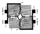
図1aのAは、本発明に従うセンサ素子の7つの異なる実施例を示す。各部分図1aのAからGにおいて、1つの実施例は、基板ベース層1上の平面図で示される。各実施例は、シリコン基板1を有し、かつ、均一な半導体層2、または、基板1を予め完全に覆っている全体層をエッチングした後に残る所望の幾何学構造の一部がその上に配置される。(残りの)均一な半導体層2の一部2aは、カンチレバーに支持された構造を有する。すなわち、一端が支持された部分2aは、決定される物理的変数の影響により偏向可能なように、基板1内にエッチングされたキャビティ6の上に配置される。一端が支持された部分2a、または、均一な半導体層2は、数量不定のアンカーポイント3を介し、基板1に接続される。一端が支持された部分2aの偏向により、材料(均質な半導体層2の容量材料)における分極が変化し、その結果、材料内における電荷担体密度が変化するか、または、均質な半導体層2の上にさらなる層が適用されることにより、材料表面、または、異なる表面との接合面にヘテロ構造が表れた場合、シリコン基板1上のキャビティ6の端に適用され、均質な半導体層2またはそのアンカーポイント3上に配置され、かつ、半導体層に当接するコンタクト5により、前記へテロ構造には、好ましくは、変化する電流が流される。図1aのAにおいて、均質な半導体層2の片持ちされた偏向可能な部分2aは、基本的にY字形のバーであるように、3つのアンカーポイント3を介し、基板ベース1に接続される。3つのアンカーポイント3と、3つの関連するコンタクト5a−5cとは、Y字または対応するバーの3つの端部に配置される。Y字バー形状は、小さな機械的偏向により電荷担体密度において大きな変化が期待できるという効果をもたらす。図1aのBにおいて、均質な半導体層2の片持ちされた偏向可能な部分2aは、基本的にU字形であるように、エッチングされたキャビティ6の同じ側にある均質な半導体層2の2つのアンカーポイント3を介し、基板ベース1に接続される。2つのアンカーポイントと、関連するコンタクト5aおよび5bとは、U字または対応するバーの両端に配置され、結果的に、キャビティ6の同じ側端部に配置されることになる。U字バーを用いることにより、直線の二重固定バーを用いた場合と同様に、反対方向の湾曲により生ずる補償なしに、基板端部近くに湾曲歪みをもたらす効果を測定することができる。図1aのCおよびEは、片持ちされた偏向可能な部分2aが、4つのアンカーポイント3を介し、基本的にXまたはH字バーとなるように基板ベースに接続されている状態を示す。4つのアンカーポイントは、XまたはH字バーの4つの端部に配置される。XまたはH形状構造は、異なる測定経路の選択を可能にするか、または、4つのコンタクト5a−5dの中から信号タッピングに用いられるコンタクトの選択を可能にする効果をもたらす。図1aのDは、均質な半導体層2の片持ちされた偏向可能な部分2aが基本的に二重の櫛形バーであるように、多数のアンカーポイント3を介し、基板ベース1に接続されるケースを示す。アンカーポイント3またはコンタクト5aおよび5bは、櫛の歯の端、または、個別のバーの端にそれぞれ配置される。櫛形のバーは、普通の直線のバーに比べ感度が優れているという利点をもつ。図1aのFは、均質な半導体層2の片持ちされた偏向可能な部分2aが、線形バーになるように、正確には1つのアンカーポイント3を介し、基板ベース1に接続されているケースを示す。アンカーポイント3は、バーの一端に配置され、該アンカーポイント3には第1のコンタクト5が配置される。対向するコンタクト(図示せず)は、自由バー端で部分2a内に一体化される。図1aのGは、片持ちされた偏向可能な部分2aが、正確には2つのアンカーポイント3を介し基板ベース1に接続されるケースを示す。ここでは、両側が固定された片持ちされた線形バーが生成される。2つのアンカーポイント3は、関連するコンタクト5aおよび5bと同じように線形バーの両端に位置する。少なくとも2つの真向かいに位置するアンカーポイント3をもつ構造、すなわち、上から見ると、エッチングされたキャビティ6の2つの対向する側に位置するアンカーポイント3は、中心の偏向により、対応するバーを介し、表面全体を歪ませることが可能であり、すなわち、曲げ半径における拡張、圧縮と同様に、バーの伸長、ひいては基本セルの拡張ができるようになるという利点をもつ。
Figure 1 a of A shows the seven different embodiment of the sensor device according to the present invention. In each
図1bおよび1cは、本発明に従うさらなる2つのセンサ構造を示す。これらのセンサ構造は、図1aのFに示されたセンサ構造と似通った構成を有する。すなわち、半導体層2の支持されていない側2a(図の右側)がキャリアに接続されていない状態で、基板1の片側(図の左側)だけに配置される。2つの図示された構造は、基板1の一部に配置され、かつ、エッチングされたキャビティ6の上で片持ちされた部分(領域2a)内に配置される窒化ガリウムバッファ層2を有する。窒化アルミニウムガリウム9からなるメサ状のカバー層9は、基板1の上の一部分と、エッチングされたキャビティ6の上の一部分とにメサがくるように、窒化ガリウムバッファ層2a上に配置される。オームコンタクト(図では5aおよび5bの2つのコンタクトとしているが、それより多数のコンタクトが適用可能である)は、支持領域(上記構造1)から支持されていない半導体領域(上記エッチングされたキャビティ6)までの遷移の端に適合される。図1bで示される構成では、2つの接点5aおよび5bは、メサ9においてバーの伸長に対し横方向(基板1のキャビティ6への方向、または、図における左から右の方向)に適合される。コンタクト5bは遷移前、コンタクト5aは、遷移後である。支持されていない領域2aにおける遷移の後ろに適合されたオームコンタクト5aは、メサ9に沿う給電線11により遷移の前の領域へと電気的に誘導される。第2のコンタクト5bにもこのような給電線11が同様に設けられる。図1cで示される構成においては、2つのオームコンタクト5aおよび5bは、バーの伸長に対し長手方向に適合される。一方は、メサ9の上端、もう一方は、メサ9の下端である。この場合、コンタクト5aおよび5bは、基板1の上の支持された領域から支持されていない領域2aへと半導体材料2が遷移する領域と交差する。トランジスタのゲート(好ましくは、ショットキーコンタクト形式)に類似した制御コンタクト10をオームコンタクト5aおよび5bの1つから一定の間隔をおいて任意に配置することも可能である(図中折線で示す)。前記間隔は、0.3ミクロンメートルから0.5ミクロンメートルが好ましい。ゲート10にも同様に給電線11が設けられる。さらなる制御コンタクトまたはゲートを同様に配置または使用することも可能である。
Figure 1 b and 1 c show two sensor structure comprising Sara according to the present invention. These sensor structure has a configuration in which similar sensor structure shown in F of FIG. 1 a. That is, the semiconductor layer 2 is disposed only on one side (left side in the figure) of the
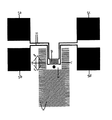
図2aは、本発明に従う加速度センサを示す。この加速度センサは、平面図に示した通りであり、その基本的な構造は、図1で示された(同一の構成要素は同一の参照番号が付されている)センサ構造に対応する。加速度センサは、窒化ガリウムからなり、かつ、四分の一円形状に形成される2つの片持ちされたバー2aを有する。前記バーは、シリコン基板1の基板端部で2つのアンカーポイント3にそれぞれ装着される。各バー2aは、図示されたセクションの四角いエッチングされないキャビティ6の端部に相互に当接する2つのアンカーポイント3を有する。アンカーポイント3またはバー2aは、均一な半導体層2の窒化ガリウムからなる部分2bを介し互いに接続される。前記部分は、片持ちされておらず、基板端部1aの近く、または、キャビティ6の端部に配置される。前記部分2bは、各バー2aの2つのアンカーポイント3をそれぞれ接続する。コンタクト5は、部分2bの上に配置される。片持ちされた部分2aの上には、図示されたセクションにおける四角い振動質量4が加速度センサの中心部分として配置される。前記質量は、エッチングされたキャビティ6の上にすべて位置し、かつ、2つの湾曲したバー2a、または、関連する4つのアンカーポイント3だけを介して基板ベースに接続される。構造8の重要性は、図2b(図2aの加速度センサの一部を示す)の説明において明らかにする。センサを加速した場合、振動質量4は、その無効位置から偏向される。振動質量4の偏向により、バー部分2aが変形し、その結果、基板端部における測定ストリップ2aの抵抗に変化が生じる。測定ストリップの抵抗における変化は、ホイートストン回路を介し、コンタクト5を用いて測定される。センサ構造または回路は、動作ポイントの調整または補償に用いられるゲート(好ましくは、ショットキー回路のような、例えば厚さ200ナノメートル、好ましくは、20ナノメートルのニッケル層および銀層のメタライゼーションによる)を任意で備えてもよい。
FIG. 2a shows an acceleration sensor according to the invention. This acceleration sensor is as shown in the plan view, and its basic structure corresponds to the sensor structure shown in FIG. 1 (the same components are given the same reference numerals). The acceleration sensor has two cantilevered
図2bは、図2aに示された加速度センサの一部を示す。均質な半導体層2の部分2aおよび2bは、領域8a、8b、および、9を除くすべての場所にメタライゼーション層を含む。それによって、領域9は、図示されたアンカーポイント3の上に直接配置され、一部片持ちされ(領域9の下部分)、一部片持ちされない(領域9の上部分またはアンカーポイントの上)。部分8a、8b、および、9は、均質な半導体層2の隆起した領域またはメサ領域を表わす。すなわち、2aおよび2bの残りの領域に対し均質な半導体層2の厚みが増す領域である。窒化ガリウムからなる均質な半導体層2の代わりに、窒化アルミニウムガリウム/窒化ガリウムからなるヘテロ構造を用いた場合、該へテロ構造は、領域9、8a、および、8b内だけに現れ、残りの領域2aおよび2bには、窒化ガリウムからなり、かつ、メタライゼーションを含むバッファ領域だけが現れる。その後、メサ部分8a、8b、および、9は、抵抗器とされる。図示された加速度センサの場合、領域9は、すべてメサであり、また、ここだけメタライゼーションが中断されるので、使用される電気信号は、メサ領域9におけるアンカーポイント3の領域内、または、支持されない領域から固定される領域までの対応する遷移領域内で半孤2aごとに生成される。基板上に固定された状態で配置された均質な半導体層2の支持されていないバー2aの残りの領域および部分2bの残りの領域には、バッファ材料(窒化ガリウム容量材料)だけが残る。前述の構成では、完全に閉じたメタライゼーションが最上部にあるので、部分9に対応しない片持ちされた部分2aの領域(領域9と振動質量への遷移領域との間の部分、および、振動質量の領域において支持されていない領域)内の信号変化は活用されない。均質な半導体層2の部分2bにおいては、半導体層2が屈曲しないので、信号は生成されない。すでに述べたように、図示された構成の測定ストリップの抵抗における変化は、ホイートストン回路を介し、コンタクト5を用いて測定される。図示された構成においては、構造および動作モードは、アンカーポイント3における未知の抵抗器と(図示された構成における合計2つの抵抗器9、図2a参照)、および、同じく未知の、前記抵抗器9と同様に生成され、同一の抵抗値を有する抵抗器8aおよび8bとを有するホイールストンブリッジに対応する。抵抗器8aおよび8b(合計4つ、図2A参照)は、並列回路におけるメタライゼーションによる、窒化ガリウムバーからなる4つの同一の支持されていない抵抗器であり、偏向されていない。振動質量4の偏向と同時に、4つの抵抗器9は、アンカーポイント3で変化するが、4つの抵抗器8は変化しないため、測定信号(または電流)は、結果として異なったものとなる。光あるいは温度といったすべての妨害の影響が抵抗器8同様抵抗器9にも同様に及ぶことにより、信号差を生じさせることなく振動質量4の本来の偏向を生じる。 抵抗器8および/または9は、任意でショットキーコンタクトのようなゲートにより構成されてもよい(図示せず)。
Figure 2 b shows a portion of the acceleration sensor shown in FIG. 2 a. The
図2cおよび2dは、さらなる加速度センサを示す。前記図で示される加速度センサの基本構造は、図2aおよび2bの加速度センサに対応するが、違いは、4つの抵抗器(9R1、9R3、9R5および9R7)をアンカーポイント3に追加した点である。前記抵抗器は、質量4の偏向と同時に生じる信号を増加させる目的で、振動質量4から支持されていないバー2aまでの遷移 (遷移領域7)において協働する。(図中、遷移領域7における抵抗器は、参照符号9R2、9R4、9R6および9R8を付して示す。)質量4の偏向と同時に、遷移領域7は、アンカーポイント3において偏向領域と正反対の方向に湾曲するため、反対方向の効果が期待できる。配線において、抵抗器は、効果が累加されるようにホイーストンブリッジ内に電気的に配置される。例えば、9R1が下方に偏向されると、9R2は、上方に偏向される。これは、9R7(下方)および9R8(上方)に関しても同様である。9R1が上述の偏向により大きくなると仮定した場合、9R7(および9R3、9R5)も同様に大きくなり、抵抗器9R2および9R8(同じく9R4および9R6も)は小さくなる。しかしながら、対の抵抗器9R1と9R7、および、9R2と9R8は、回路内の「交差点」に電気的に配置されているため、効果が累加され、偏向している間に、高電荷および高測定信号が生じることになる。これは、偏向していない状態とは対照的である。回路の原理を図2dに再び示す。参照符号5aおよび5bは、測定に必要な入力電圧(Uin)が印加されるコンタクトを示し、参照符号5cおよび5dは、測定の間に電圧または電流がタップされるコンタクトである。図示された回路内では、動作前のブリッジは、0に調整されていなければならない。そのため、例えば、測定ポイント5cおよび5dにおける電流は、コンタクト5bおよび5aに電圧が印加されるときに測定される。 その結果、偏向なしの値が生成される。電流における変化のすべては、抵抗器9の偏向に変化が起きると同時に生じ、抵抗器9またはその値が正確に知られることなしに偏向の測定値となる。(さもなければ、ホイートストン回路の平均)。また、抵抗器は、ゲート(図示せず)によって構成されてもよい。妨害の影響は、図2bの抵抗器8と同様に、偏向されない基準抵抗器を介し較正されることができる。抵抗器9が個別に電気的アクセス可能にされる場合、または、適切な配線によりいわば電気的に起動される場合、すなわち、抵抗器9の個々の抵抗値が測定される場合、質量4の対称な偏向がもう生成されず、その結果、抵抗器9もそれらの値を場所の関数として変更するので、質量4の偏向方向を示すこともできる(例えば、地面の上の車の位置など)。
Figures 2c and 2d show a further acceleration sensor. Point the basic structure of the acceleration sensor shown in the figure, but correspond to the acceleration sensor of Fig. 2 a and 2 b, the difference is added four resistors (9R1,9R3,9R5 and 9R7) to the
図2eおよび図2fは、支持されないバー形式でのさらなる加速度センサを示す。以降説明するこのセンサは、加速度以外の物理的変数を検出するセンサと類似した構造内で用いることもできる。窒化ガリウムからなる均質な半導体層2の支持されないバー2aは、矩形のメサ9、または、対応する隆起した部分9を有する。窒化アルミニウムガリウム/窒化ガリウムからなるヘテロ構造の場合、窒化アルミニウムガリウムのカバー層は、メサ領域9における窒化ガリウムからなるバッファ層上に存在する。図示されたケースにおけるコンタクトは、ファン・デル・ポーによる4ポイント構造である。すなわち、メサ9は、その4つのコーナーで、給電線11を介しコンタクト5a−5dに接続される。分離線Tの上の領域(すなわち領域To)において、均質な半導体層2は、片持ちされておらず、分離線Tの下の領域(領域Tu)では、均質な半導体層2は、片持ち状とされる。(領域2a)。メサ9は、片持ち状とされた領域から片持ちされていない領域までの遷移領域に配置されるか、または、一部が均質な半導体層2の片持ちされない側に、また、一部が片持ちされる側に配置される(均質な半導体層の領域2a)。図示された加速度センサの場合、信号は、ホール効果により決定される。層導電率およびホール抵抗が決定されると、そこから電荷担体のタイプ、電荷担体密度、および、電荷担体可動性が決定できる。ファン・デル・ポーによる4ポイント構造としての実施例に代わり、ホールバー構造として回路を構成することもできる。コンタクト5a−5dは、オームコンタクトであり、窒化ガリウムバッファ上に給電線11を走らせる。
Figure 2 e and FIG. 2 f shows a further acceleration sensor with unsupported bar format. This sensor described below can also be used in a structure similar to a sensor that detects physical variables other than acceleration. The
図2gおよび2hは、ホール効果測定方法とともに用いられるファン・デル・ポー構造の他の実施例を示す。均質な半導体構造膜2、および、上からエッチングするための4つの開口12aから12dの走査型電子顕微鏡による図であり、4つの給電線13、および、4つのオームコンタクト14も示されている(給電線13は、コンタクト14から内側方向、すなわち、開口12の領域へと先細りに延びる)。
Figure 2 g and 2 h show another embodiment of a van der Pauw structure for use with the Hall effect measuring method. FIG. 2 is a view of a homogeneous semiconductor structure film 2 and four
エッチング終了後、支持されていない膜部分2cが画像の中心領域(領域2c)に生成される。この部分は、機械力または流れ圧力などにより偏向可能である。 After the etching is completed, an unsupported film portion 2c is generated in the central region (region 2c) of the image. This portion can be deflected by mechanical force or flow pressure.
図3aは、本発明に従う圧力センサを示し、図1および2ですでに説明したセンサと同じ構成要素を有する。本実施例の圧力センサの場合、窒化ガリウムからなる均質な半導体層2の片持ちされた偏向可能な部分2aは、円形膜2cとして形成される。アンカーポイント3の領域において、膜2cは、2つのメサ、または、隆起した部分9aおよび9bを有し、この場合、窒化ガリウム層上に窒化アルミニウムガリウム層が配置される。前記メサまたは抵抗領域には、窒化アルミニウムガリウム/窒化ガリウムへテロ構造だけが存在する。膜2cの両側における圧力が異なる場合、抵抗領域9が隆起する。その下にあるエッチングされたキャビティ6も、同じく円形である。隆起により、基板端部の膜2c(基板端部1aにおける片持ちされた部分2aおよび片持ちされない部分2b)はその分極状態の変化における結果として変形する。ヘテロ構造チャネルまたはメサ領域9aおよび9bにおいて、窒化アルミニウムガリウム層と窒化ガリウム層との間の接合面で電荷担体密度および累積が生じ、コンタクト5により出力信号として伝達される。コンタクト5は、窒化アルミニウムガリウム/窒化ガリウム積層のヘテロ構造チャネルに直接配置される。
Figure 3 a shows a pressure sensor according to the present invention has the same components as sensor previously described in FIGS. 1 and 2. In the case of the pressure sensor of this embodiment, the cantilevered
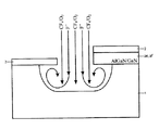
出力信号とその変化は、抵抗バー、または、メサ領域9aおよび9bを介し測定される。膜2cの上側と下側との圧力差は、抵抗バーまたはメサ領域9aおよび9bの隆起を介し測定される。センサの温度独立性は、ホイートストン回路により確立される。このホイートストンブリッジの補正機能のためには、2つの一定標準抵抗が必要である。主要膜2cの左右2つの半円膜2dのアンカーポイントにおける2つの抵抗器9cおよび9dは、この要件を満たす。膜2cの場合と同様に、膜2dにおいては、抵抗またはメサ領域9内だけにヘテロ構造が存在する(あるいは窒化ガリウムバッファ内だけ)。両方の膜2dは、窒化ガリウムバッファが除去された領域を有し(極左または極右領域6aおよび6b)、その結果、圧力差が無くなり、膜2dは歪みなしで形成されることが可能になる。結果的には、抵抗器9cおよび9bのどちらも非圧力依存性のままであるが、回路が温度の影響を受けないようする非温度依存性ではない。基板端部1a全体における歪みが均等なることにより、膜の周囲の形状が幾何学的に生じ、膜2cは、最大安定度を得ることができる。ここで任意に用いられ、かつ、好ましくはショットキーコンタクトのように構成されるゲート(図の左下10)は、動作ポイントを調整する役割を果たす。図3aに示される圧力センサの回路動作モードは、図2aから2dにおいて説明された加速度センサの回路動作モードと同じである。すなわち、4つの抵抗器9a−9dが用いられ、そのうち2つの抵抗器9aおよび9bは、アネロイドダイヤフラムまたは膜2c上にあり、他の2つの抵抗器9cおよび9dは、半円形膜2d上にある。すでに述べたように、膜2cは、アネロイドダイヤフラムまたは膜2cの下に封じ込められたガス容量に比べ、膜2cの上の圧力が高いかまたは低い場合に偏向されることができる。窒化ガリウムバッファ(6aおよび6b)が取り除かれた領域をもつことにより、膜2dには封じ込められたガス容量が存在しないので、該膜2dは、偏向されず、抵抗器9cおよび9dが基準抵抗としての役割を果たす。圧力が変化した場合、ダイヤフラム2c上の2つの抵抗器9aおよび9bは変化するが、他の2つの基準抵抗器9cおよび9dは変化しない。4つの抵抗器9a―9dのホイートストンブリッジにより、電流の変化(4つの抵抗器すべておよび2つの基準抵抗器9cおよび9dに均等に作用する、例えば温度などによる妨害は偏向されないので、それとは無関係)は、抵抗器9の値を再び実際に認識しなくても、測定することが可能になる。有効な抵抗器9a―9dは、支持された半導体2bが支持されない半導体2aに遷移する領域3に位置し、すでに述べたように、メサ状に形成される。すなわち、膜2cおよび2dそれ自体だけで窒化ガリウムバッファを構成するようになる。図2a−2dで用いられたホイートストン回路に比べ、抵抗器9aおよび9dの幅bは、より高い効果(個々のセンサ素子の並列回路がいわば抵抗器9の方向bに沿って存在するのでより高い電流)が得られるよう基本的に大きい。しかしながら、加速度センサがほとんど動作できなくなるので、このような大きい抵抗器を直ちに使用することはできない。図示されたゲート10を有する実施例に代わり、ゲートなしの他の実施例も可能である。膜の形状としては、円形または半円形(例えば矩形または四角の領域)を使用してもよい。図3bは、ダイヤフラム2cまたは基準膜2dに用いられるエッチングされないキャビティ2DIおよび2CIの走査型電子顕微鏡画像を示す。
The output signal and its change are measured via resistance bars or mesa regions 9a and 9b. The pressure difference between the upper and lower sides of the membrane 2c is measured through the bulges of the resistance bars or mesa regions 9a and 9b. Sensor temperature independence is established by a Wheatstone circuit. Two constant standard resistors are required for the correction function of the Wheatstone bridge. The two resistors 9c and 9d at the anchor points of the two left and right semicircular membranes 2d of the main membrane 2c meet this requirement. As in the case of the film 2c, in the film 2d, the heterostructure exists only in the resistor or mesa region 9 (or only in the gallium nitride buffer). Both membranes 2d have regions from which the gallium nitride buffer has been removed (extreme left or extreme
図4は、バー形状の片持ちされた能動均質半導体層を生成するために用いられる試験体の層構造を概略的に示す。試験体のベースは、約300ミクロンメートルの厚みを有するシリコン基板1を形成する。このシリコン基板上に窒化ガリウムからなる厚さ約1.7ミクロンメートルの均質な半導体層2fが適用される。次に、この半導体層2fの上に、Al0.2Ga0.8Nからなる厚さ約20ナノメートルのカバー層2eが適用される。このようにして、図示された試験体からヘテロ構造センサ素子が生成される。
FIG. 4 schematically shows the layer structure of a specimen used to produce a bar-shaped cantilevered active homogeneous semiconductor layer. The base of the specimen forms a
図5は、本発明に従うヘテロ構造センサ素子の生成における基本的ステップであるバー構造のアンダーエッチングを概略的に示す。図5を用い、本発明に従うセンサ素子を生成する半導体構造化方法の他のステップすべてを説明することもできる。まず、均質な半導体層2fとカバー層2e(窒化ガリウムまたはAl0.2Ga0.8N)の複合体から所望の表面領域のメサがエッチングされ、ベース領域の外側のヘテロ構造2eおよび2fが基板ベース1に至るまでエッチングされる。残りのメサは、図5の右上(2eおよび2fの部分)に示されている。アンダーエッチングされる領域(図右のメサ領域2eおよび2fと、図左の基板領域)は、アルミニウムマスク7で覆われる。続いて、被覆領域は、反応性ガスにハロゲンを用いる反応性イオンエッチング法によりエッチングされる。以下の例で用いられるドライエッチング法は、酸素が豊富なCF4プラズマを使用する。エッチングは、イオンの対応する加速度により生成される機械的成分(CF4/O2)、および、化学エッチング成分(フッ素イオン)により結果的に実行される。
FIG. 5 schematically shows under-etching of the bar structure, which is a basic step in the generation of a heterostructure sensor element according to the invention. FIG. 5 can also be used to describe all other steps of the semiconductor structuring method for producing the sensor element according to the invention. First, a mesa in a desired surface region is etched from a composite of a
図6は、片持ちされたバー(すなわち、非金属および非半導体材料で充填されていない離間領域を有する)、または、図5を参照して説明されたエッチングプロセスにより生成されたシリコン基板1上に、窒化ガリウムからなる片持ちされた均質な半導体層2fの基本構造を示す。片持ちされたバー2fは、シリコン基板1の左端または右端で支持される。概略的に図示されるセンサ素子の中心には、均質な半導体層2fの下のキャビティ6が示される。このキャビティは、図5で説明したエッチングプロセスにより生成されたもので、その深さdは約150ナノメートルである。片持ちされた能動均質半導体層2fの頂側部に、2つのコンタクト5a(バーの左端)、および、5b(バーの右端)が直接取り付けられることにより、バー2fの屈曲または偏向と同時に生成される電気信号をピックアップまたは伝達できるようになる。
FIG. 6 shows a cantilevered bar (i.e. having a spaced area that is not filled with non-metallic and non-semiconductor materials) or on the
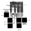
図7は、本発明に従う加速度センサの断面図である。断面は、基板表面に対し垂直である。図は、厚みd1が300ミクロンメートルであるシリコン基板1を示す。このシリコン基板1の上に均質な窒化ガリウム半導体層2fが配置される。中間部または中心部がアンダーエッチングされることにより、基板1は、層2fの下の立法形領域(キャビティ6)においては、少なくとも一部剥離し、また、該立法形領域(キャビティ6)の端部においては、完全に剥離し(その結果層2fの下側は完全に露出する)、さらに、該立法形領域の内側では、完全に剥離しないので、層2fと接している基板が残り、振動質量4を形成する。図示された構造において、均質なGaN半導体層2fは、カンチレバー保持棒または膜を形成し、該保持棒または膜は、基板1の少なくとも2つの領域(左右側に示された)と、振動質量4が半ば宙吊りになった状態で中心に装着されたその上とで支持される。振動質量4は、加速度効果により、上方または下方に偏向される(図の矢印)。基板表面から間隔を置いて面したその表面において、均質な半導体層2fは、2つの隆起した部分または2つのメサ領域を有する。各メサ領域は、基板表面と平行な方向(図では左から右)、または、半導体層2fの表面と平行な方向に延びる。各メサ領域は、均質な半導体層2fの下側が基板1から剥離する領域上で、該均質な半導体層2fが基板1によって支持される領域から、該均質な半導体層2fの下に振動質量4が配置される領域まで延びる。メサ領域外側の層2fの厚みは、図示されたケースでは、d2=1.7ミクロンメートルである(通常、好ましくは、0.5ミクロンメートルから3ミクロンメートル)。メサ領域においては、層2fの厚みは、1.93ミクロンメートルである(通常、メサ領域における層の追加の厚みは、好ましくは、170ナノメートルから290ナノメートル)。窒化アルミニウムガリウムからなるカバー層2eは、層2fのメサ上に載置され、その結果、メサ領域にヘテロ構造が形成される。カバー層2eの厚みは、20ナノメートル(通常、好ましくは、10ナノメートルから30ナノメートル)であり、その結果、メサの高さは、d3=250ナノメートルとなる(コンタクト5はなし)。図示した加速度センサは、本発明に従うヘテロ構造を有する。窒化ガリウム層2fと窒化アルミニウムガリウムカバー層2e(すなわちメサ領域)との接合面に、ヘテロ構造チャネル2gが配置される。各メサには、2つの接触領域がヘテロ構造チャネル2gと当接して配置される。それぞれの接触領域は、片持ちされない領域(すなわち基板支持1の上の領域)内、および、片持ちされる領域内の接触領域(基板層1が層2fの下から除かれる領域の上および宙吊りの振動質量4の領域内)内に配置される。図示された4つの接触領域それぞれは、半導体層2eおよび2f内のヘテロ構造チャネル2g(またはそこへの接合面)に合金することにより生成される接触領域(参照番号2hとして表される領域)と、該接触領域2hの上に適用される金属コンタクト5とを含む。金属コンタクト5には、給電線11が設けられる。振動質量4が加速度の影響により上方または下方に偏向された場合、ヘテロ構造領域内またはメサ領域内で電気信号が生成される。この電気信号が生成される領域は、参照符号Bとして表される。その後、信号は、接触領域2hを介し、伝達され、コンタクト5aから5bへ、そして給電線にも伝達される。この流れは、流れ線15として表される。その結果、接触領域は、ヘテロ構造チャネル2gに直接配置される。この場合の構造において重要な点は、抵抗領域またはメサ領域それぞれが、ヘテロ構造または層2eおよび2fの固定領域内(すなわち、ヘテロ構造または層2fがシリコン基板1により支持される領域内)に配置されること、および、抵抗領域またはメサ領域それぞれの他のコンタクトが自由に吊着された膜領域または残りのバー領域に位置していることである。図示されたケースでは、固定から自由への遷移は、メサ領域のほぼ真ん中より下である。この構造の場合、メサは、ある特定の長手方向の一部でだけ具体的に特定されるので、この長手方向の一部において生じる1つの曲線だけが結果として測定信号を生じる。メサ領域は、偏向の間に生じる曲線が最大になる領域内に好適に配置される。例えば2つのコンタクトが固定領域(すなわちシリコン基板1の上 )に配置され、かつ、膜の上に部分的に延びる閉じたヘテロ構造の長手方向部分により接続される(その結果生じた湾曲は部分的に反対方向に延びる)配置に関し、本実施例は、反対方向に延び、結果としてきわめて小さくなる曲線により生じた信号成分は考慮せず、むしろ信号成分が極めて高くなるという利点がある。図示したケースでは、膜またはバーが偏向する間に、そのために電気的閉鎖経路の長さまたは要素、あるいは、材料内の湾曲すべてが信号に寄与するわけではない。図示した配置の本発明に従う構造の場合、本質的にヘテロ構造は、メサの領域内でだけ維持され(半導体の有効な活性領域が位置する)、メサまたは対応する領域の外側において、ヘテロ構造がエッチングされ、均質層2fだけが残りの膜または残りの保持バーとして存在する。この状況では、コンタクト5は、メサ領域の外縁部に好適に配置される。図7の下部領域に図示された走査電子顕微鏡像は、立法形領域がすでにエッチングされ、振動質量4が検出できるところからシリコン基板1を見た図を示す。図7に示されたセンサ、および、その他図示されたすべてのセンサは、ヘテロ構造の形式をとらずに構成されることもできる(すなわち、均質な半導体層2fだけでもよい)。センサ機能は、メサ領域の幾何学的定義により確実なものとなる。これは、適切なエッチングによるものである。残りの膜材料(バッファまたは非メサ領域)に寄生効果が接触するのを防止するために、メサに、適切なエッチング深度(材料に従う)を与えることができる。信号または効果強度が材料のタイプに従い変化することから、効果は、バルク材料によって最大になると仮定することができる。
FIG. 7 is a cross-sectional view of an acceleration sensor according to the present invention. The cross section is perpendicular to the substrate surface. The figure shows a
図8aI、8aII、8bおよび8cは、片側に、または、アンカーポイントに装着された片持ちされたバー形式による、本発明に従うセンサ要素を示す。これらは、アンカーポイントの反対側に位置するバー端部に装着された犠牲膜により生成されたものである。予め決められた極限21を介し犠牲膜2kに最初に接続する3つのバーが図8aIおよびaIIに示されている。さらに、5aから5dの4つの電気的コンタクトが、給電線11を介し、メサ9と接続している状態が示されている。前記メサは、すでに説明したように、一部支持されていない領域に配置され、一部半導体構造層2の固定領域上に配置されている。図示された半導体構造は、以下のように生成される。まず、第1のエッチングにより、メサ9(ある割合の窒化ガリウム層2fおよび窒化アルミニウムガリウム層2e)を生成する(電流が貫流する活性領域)。第1のエッチングにおける深度は、200ナノメートルから500ナノメートルである。第2のエッチングステップにおいて、メサ9の外側に領域2f−Tがエッチングされる。前記領域は、それ自体がバー構造または片持ちされたバー構造2aを定義する(これによって窒化ガリウムの上部がエッチングされて完全に基板1に達する)。このタイプの窒化ガリウム層の構造化は、好ましくは、キャビティ6のエッチングが上述の結果もたらされるときに用いられる。キャビティ6のエッチングが裏側から行われると(図中参照符号RAとして表される)、シリコン基板を用いたICP標準方法を使用した場合と同じように、その幾何学的形状を定義する目的で、上記エッチングは十分深くまで行われる(例えば、バーまたはバー構造を定義するため部分的に「深いメサ」として指定される)。一方、前記エッチングは、2ステップで適用されることもできる。図示したケースでは、回路は、ゲート10により構成される。図示したセンサ要素は、[111]シリコン基板の上側から酸素を添加した反応ガスCF4を用いてケミカルドライエッチングすることにより生成されている。シリコン基板の[111]表面を用いるのは、III族窒化物の六角形格子構造をもつからである。エッチングは、基本的に裏側と表側から進行する。裏側からのエッチングには、標準的な方法(ICP、ボッシュプロセス)を用いることができる。裏側のエッチングは、RIE法(反応性イオンエッチング)でも実行できる。表側のエッチングは、好ましくはRIE法によって実行される。前述ように予め決められた極限21をもつ犠牲膜2kが用いられた場合、極めて長く細いバーを生成することができる。例えばバーの幅がわずか1ミクロンメートルであるのに対し長さは100ミクロンメートルにできる。このようなバーは、犠牲膜2kを次の支持されていないバー端部2aに適用して、(予め決められた極限2kをもつ膜への機械的圧力による)エッチング後に実際のバー2aから除去することにより得られる。図8bは、予め決められた極限21を介し犠牲膜2kとまだ接続した状態の2つのバー2aが見える操作電子顕微鏡像を示す。図8cは、前述のように生成された3つの細い支持されていないバー2a1、2a2、および、2a3を示す。一番上のバー2a1は、長さ100ミクロンメートル、幅1ミクロンメートルを有する。
FIGS. 8aI, 8aII, 8b and 8c show a sensor element according to the invention, in the form of a cantilever bar attached to one side or to an anchor point. These are produced by a sacrificial film attached to the end of the bar located on the opposite side of the anchor point. The three bars that initially connect to the
Claims (69)
基板ベースと、
前記基板ベース上に配置された半導体層とを含み、
前記半導体層は、前記基板ベースに対して片持ちまたは両持ちされており、接合面を介して前記基板ベースと部分的に直接接し且つ前記基板ベースと部分的に直接接しておらず、III族窒化物半導体化合物を含む均質な半導体層または互いに接した2つだけの均質な半導体層を含むIII族窒化物半導体化合物のヘテロ構造であり、
半導体センサ素子により決定される物理的変数における変化に基づき、前記半導体層により生成されることができる電気出力信号を伝達するための少なくとも2つの導電コンタクトが前記半導体層に直接接して設けられることを特徴とする、半導体センサ素子。A semiconductor sensor element,
A substrate base;
A semiconductor layer disposed on the substrate base,
The semiconductor layer is cantilevered or both-sided with respect to the substrate base, is partly in direct contact with the substrate base via a bonding surface, and is not partly in direct contact with the substrate base. A heterostructure of a III-nitride semiconductor compound comprising a homogeneous semiconductor layer comprising a nitride semiconductor compound or only two homogeneous semiconductor layers in contact with each other;
Based on a change in a physical variable determined by a semiconductor sensor element, at least two conductive contacts are provided in direct contact with the semiconductor layer for transmitting an electrical output signal that can be generated by the semiconductor layer. A semiconductor sensor element.
前記離間領域から前記非離間領域への遷移は、前記隆起した領域またはメサ領域の中心領域内で前記均質な半導体層に面した基板ベースの表面と平行な方向に実行されることを特徴とする、請求項2に記載の半導体センサ素子。 The homogeneous semiconductor layer has raised or mesa regions;
Transition from the separation region to the non-separated region, characterized in that it is performed in the raised areas or a direction parallel to the homogeneous semiconductor layer facing the substrate base surface in the central region of the mesa The semiconductor sensor element according to claim 2.
基板ベース上に配置された半導体層を含み、前記半導体層は、前記基板ベースに対して片持ちまたは両持ちされており、接合面を介して前記基板ベースと部分的に直接接し且つ前記基板ベースと部分的に直接接しておらず、
前記半導体層として、III族窒化物半導体化合物を含む均質な半導体層またはIII族窒化物半導体化合物を有する互いに接した2つだけの均質な半導体層を含むヘテロ構造が使用され、
前記半導体層により決定される物理的変数における変化に基づき、前記半導体層により生成されることができる電気出力信号を伝達するための少なくとも2つの導電コンタクトが前記半導体層に直接接して設けられ、
前記半導体層における前記物理的変数における変化に基づき、電気出力信号を生成し、該出力信号を、前記少なくとも2つの導電コンタクトを介し伝達する工程を備える、測定方法。A measurement method for determining a change in a physical variable, comprising:
A semiconductor layer disposed on the substrate base, wherein the semiconductor layer is cantilevered or both-sided with respect to the substrate base, and is in direct contact with the substrate base through a bonding surface and the substrate base; Is not directly in contact with
As the semiconductor layer, a heterostructure including a homogeneous semiconductor layer containing a group III nitride semiconductor compound or only two homogeneous semiconductor layers in contact with each other and having a group III nitride semiconductor compound is used.
Based on a change in a physical variable determined by the semiconductor layer, at least two conductive contacts for transmitting an electrical output signal that can be generated by the semiconductor layer are provided in direct contact with the semiconductor layer;
A measurement method comprising the steps of generating an electrical output signal based on a change in the physical variable in the semiconductor layer and transmitting the output signal through the at least two conductive contacts.
III族窒化物半導体化合物を含む均質な半導体層またはIII族窒化物半導体化合物を含む互いに接した2つだけの均質な半導体層から構成され、エッチングされるメサの基礎領域に対応する領域上の基板ベースと間隔を置いて面している表面にマスクが施される積層半導体を前記基板ベース上に配置する工程と、
前記積層半導体のエッチングされるメサの前記基礎領域に対応した前記領域に、生成される離間領域に当接する領域内の前記基板ベースに被さらないようにエッチングマスキングする工程と、
前記積層半導体を、前記基礎領域に対応する前記領域の外側から前記基板ベースに至るまでエッチングする工程と、
少なくとも2つの導電コンタクトまたは電気コンタクト層を前記積層半導体に直接接して設ける工程とを備え、
前記エッチングする工程において、前記離間領域に当接する領域内と、前記エッチングマスキングおよび前記均質な半導体層の下の前記離間領域内との両方において前記基板ベースをエッチングするか、または、前記離間領域において前記エッチングマスキングおよび前記均質な半導体層をアンダーエッチングし、
前記均質な半導体層は、前記基板ベースに接続されており、前記基板ベースに面した前記基礎領域においては前記基板ベースと少なくとも部分的に当接しないかまたは離れていることを特徴とする、製造方法。A method for manufacturing a semiconductor sensor element according to any one of claims 1 to 49,
A substrate on a region corresponding to the base region of the mesa to be etched, composed of a homogeneous semiconductor layer containing a group III nitride semiconductor compound or only two homogeneous semiconductor layers in contact with each other containing a group III nitride semiconductor compound Placing on the substrate base a laminated semiconductor that is masked on the surface facing the base and spaced apart;
Etching masking the region corresponding to the base region of the mesa to be etched of the stacked semiconductor so as not to cover the substrate base in a region in contact with the generated separation region;
Etching the laminated semiconductor from the outside of the region corresponding to the base region to the substrate base;
Providing at least two conductive contacts or electrical contact layers in direct contact with the laminated semiconductor,
In the etching step, the substrate base is etched both in a region abutting the spaced region and in the spaced region under the etching masking and the homogeneous semiconductor layer, or in the spaced region Underetching the etching mask and the homogeneous semiconductor layer;
Manufacturing, characterized in that the homogeneous semiconductor layer is connected to the substrate base and in the basic region facing the substrate base at least partly does not abut or is separated from the substrate base Method.
Applications Claiming Priority (3)
| Application Number | Priority Date | Filing Date | Title |
|---|---|---|---|
| DE10311757.1 | 2003-03-18 | ||
| DE10311757 | 2003-03-18 | ||
| PCT/EP2004/002817 WO2004083110A2 (en) | 2003-03-18 | 2004-03-18 | Sensor element with self-supporting bar structures made of group iii nitride based semiconductors |
Publications (2)
| Publication Number | Publication Date |
|---|---|
| JP2006520536A JP2006520536A (en) | 2006-09-07 |
| JP5057778B2 true JP5057778B2 (en) | 2012-10-24 |
Family
ID=33015904
Family Applications (1)
| Application Number | Title | Priority Date | Filing Date |
|---|---|---|---|
| JP2006504725A Expired - Fee Related JP5057778B2 (en) | 2003-03-18 | 2004-03-18 | Semiconductor sensor element and manufacturing method made of group III nitride semiconductor, and measuring method using the semiconductor sensor element |
Country Status (4)
| Country | Link |
|---|---|
| US (1) | US7504658B2 (en) |
| EP (1) | EP1606600A2 (en) |
| JP (1) | JP5057778B2 (en) |
| WO (1) | WO2004083110A2 (en) |
Families Citing this family (16)
| Publication number | Priority date | Publication date | Assignee | Title |
|---|---|---|---|---|
| JP2005300493A (en) * | 2004-04-16 | 2005-10-27 | Nippon Telegr & Teleph Corp <Ntt> | Semiconductor displacement-detecting element and detector |
| US8033178B2 (en) | 2005-12-31 | 2011-10-11 | Endress + Hauser Gmbh + Co. Kg | Pressure-measuring cell |
| US7939994B2 (en) * | 2006-05-17 | 2011-05-10 | Microgan Gmbh | Micromechanical actuators comprising semiconductors on a group III nitride basis |
| CN101583559B (en) * | 2006-11-10 | 2012-02-15 | 新加坡科技研究局 | A micromechanical structure and a method of fabricating a micromechanical structure |
| DE102008009215A1 (en) * | 2008-02-13 | 2009-08-20 | Universität Kassel | Component for displaying symbols and optical display device produced therewith |
| US9970897B2 (en) * | 2008-06-16 | 2018-05-15 | Duke University | Chemical sensors and methods for making and using the same |
| US9958442B2 (en) | 2009-02-11 | 2018-05-01 | Duke University | Sensors incorporating antibodies and methods of making and using the same |
| FR2944274B1 (en) * | 2009-04-10 | 2012-03-02 | Centre Nat Rech Scient | PIEZOELECTRIC MICROELECTROMECHANICAL DEVICE |
| JP5380754B2 (en) * | 2010-02-12 | 2014-01-08 | 日立金属株式会社 | Method for manufacturing nitride semiconductor free-standing substrate and method for manufacturing nitride semiconductor device |
| EP2461145B1 (en) * | 2010-12-01 | 2013-10-09 | Honeywell International Inc. | Pressure sensor with Schottky diode |
| FR2971243B1 (en) | 2011-02-09 | 2013-03-08 | Centre Nat Rech Scient | MICROELECTROMECHANICAL DEVICE WITH PIEZOELECTRIC ACTUATION STRUCTURE |
| US10407716B2 (en) | 2014-03-13 | 2019-09-10 | Duke University | Electronic platform for sensing and control of electrochemical reactions |
| EP3313777B1 (en) * | 2015-06-26 | 2020-11-04 | Intel Corporation | Group iii-n mems structures on a silicon substrate |
| FR3047841B1 (en) | 2016-02-17 | 2018-05-25 | Centre National De La Recherche Scientifique | ELECTROMECHANICAL TRANSDUCER BASED ON GALLIUM NITRIDE DOPE. |
| US11137310B2 (en) * | 2017-10-16 | 2021-10-05 | Thomas P. White | Micro-hall effect devices for simultaneous current and temperature measurements for both high and low temperature environments |
| JP6390807B1 (en) * | 2018-03-02 | 2018-09-19 | 富士電機株式会社 | Power converter |
Family Cites Families (12)
| Publication number | Priority date | Publication date | Assignee | Title |
|---|---|---|---|---|
| US4204185A (en) * | 1977-10-13 | 1980-05-20 | Kulite Semiconductor Products, Inc. | Integral transducer assemblies employing thin homogeneous diaphragms |
| DE68926601T2 (en) * | 1988-09-02 | 1997-01-23 | Honda Motor Co Ltd | Semiconductor sensor |
| DE19961578A1 (en) * | 1999-12-21 | 2001-06-28 | Bosch Gmbh Robert | Sensor comprises a micromechanical structure based on silicon integrated in the sensor chamber of a base wafer and a cover made of a transparent deposition layer and a sealing layer |
| US7189358B2 (en) | 2000-08-08 | 2007-03-13 | California Institute Of Technology | Integrated micropump analysis chip and method of making the same |
| US6579068B2 (en) * | 2000-08-09 | 2003-06-17 | California Institute Of Technology | Method of manufacture of a suspended nitride membrane and a microperistaltic pump using the same |
| US6355498B1 (en) * | 2000-08-11 | 2002-03-12 | Agere Systems Guartian Corp. | Thin film resonators fabricated on membranes created by front side releasing |
| US6647796B2 (en) * | 2000-08-11 | 2003-11-18 | California Institue Of Technology | Semiconductor nitride pressure microsensor and method of making and using the same |
| JP2002170962A (en) * | 2000-09-25 | 2002-06-14 | Fuji Photo Film Co Ltd | Semiconductor pressure sensor |
| JP3856750B2 (en) * | 2001-11-13 | 2006-12-13 | 松下電器産業株式会社 | Semiconductor device and manufacturing method thereof |
| US7086288B2 (en) | 2002-11-27 | 2006-08-08 | Northwestern University | Thin membrane transducer |
| JP2007516746A (en) | 2003-12-11 | 2007-06-28 | プロテウス バイオメディカル インコーポレイテッド | Implantable pressure sensor |
| US7181972B2 (en) | 2004-12-27 | 2007-02-27 | General Electric Company | Static and dynamic pressure sensor |
-
2004
- 2004-03-18 WO PCT/EP2004/002817 patent/WO2004083110A2/en active Application Filing
- 2004-03-18 EP EP04721498A patent/EP1606600A2/en not_active Withdrawn
- 2004-03-18 US US10/549,438 patent/US7504658B2/en not_active Expired - Fee Related
- 2004-03-18 JP JP2006504725A patent/JP5057778B2/en not_active Expired - Fee Related
Also Published As
| Publication number | Publication date |
|---|---|
| US7504658B2 (en) | 2009-03-17 |
| WO2004083110A3 (en) | 2005-03-24 |
| JP2006520536A (en) | 2006-09-07 |
| WO2004083110A2 (en) | 2004-09-30 |
| EP1606600A2 (en) | 2005-12-21 |
| US20070176211A1 (en) | 2007-08-02 |
Similar Documents
| Publication | Publication Date | Title |
|---|---|---|
| JP5057778B2 (en) | Semiconductor sensor element and manufacturing method made of group III nitride semiconductor, and measuring method using the semiconductor sensor element | |
| US7404247B2 (en) | Method for making a pressure sensor | |
| US5543349A (en) | Method for fabricating a beam pressure sensor employing dielectrically isolated resonant beams | |
| JP3481627B2 (en) | Dielectrically separated resonant microsensor | |
| US5702619A (en) | Method for fabricating a high pressure piezoresistive transducer | |
| US6275137B1 (en) | Semiconductor piezoresistor | |
| US9038443B1 (en) | Microfabricated resonant fluid density and viscosity sensor | |
| WO1993018382A1 (en) | Soi actuators and microsensors | |
| US8033178B2 (en) | Pressure-measuring cell | |
| WO2008013982A1 (en) | Nano electromechanical resonator | |
| WO2015049598A1 (en) | Mems pressure sensor with a high electron mobility transistor and a production method thereof | |
| Lhermet et al. | First microphones based on an in-plane deflecting micro-diaphragm and piezoresistive nano-gauges | |
| Qaradaghi et al. | Frequency output MEMS resonator on membrane pressure sensors | |
| JPH08261853A (en) | Mechanical-quantity sensor element | |
| JP5030163B2 (en) | Micromechanical resonator and manufacturing method thereof | |
| Chen et al. | Design and modeling of a silicon nitride beam resonant pressure sensor for temperature compensation | |
| US11099205B2 (en) | Prestrained vibrating accelerometer | |
| CN111157762B (en) | High-sensitivity nanowire acceleration sensor | |
| CN218633882U (en) | MEMS resonator | |
| JPH04304679A (en) | Pressure sensor | |
| JP5007912B2 (en) | Structure with semiconductor beam | |
| JPH08293615A (en) | Vibrating pressure sensor | |
| Lee et al. | Fabrication of high-temperature silicon pressure sensor using SDB-SOI technology | |
| JP2005181232A (en) | Electromechanical converter and its manufacturing method | |
| JP5849663B2 (en) | Method for manufacturing vibration transducer |
Legal Events
| Date | Code | Title | Description |
|---|---|---|---|
| A621 | Written request for application examination |
Free format text: JAPANESE INTERMEDIATE CODE: A621 Effective date: 20070202 |
|
| A131 | Notification of reasons for refusal |
Free format text: JAPANESE INTERMEDIATE CODE: A131 Effective date: 20110118 |
|
| A601 | Written request for extension of time |
Free format text: JAPANESE INTERMEDIATE CODE: A601 Effective date: 20110418 |
|
| A602 | Written permission of extension of time |
Free format text: JAPANESE INTERMEDIATE CODE: A602 Effective date: 20110425 |
|
| A601 | Written request for extension of time |
Free format text: JAPANESE INTERMEDIATE CODE: A601 Effective date: 20110518 |
|
| A602 | Written permission of extension of time |
Free format text: JAPANESE INTERMEDIATE CODE: A602 Effective date: 20110525 |
|
| A521 | Request for written amendment filed |
Free format text: JAPANESE INTERMEDIATE CODE: A523 Effective date: 20110620 |
|
| A131 | Notification of reasons for refusal |
Free format text: JAPANESE INTERMEDIATE CODE: A131 Effective date: 20120313 |
|
| A521 | Request for written amendment filed |
Free format text: JAPANESE INTERMEDIATE CODE: A523 Effective date: 20120613 |
|
| TRDD | Decision of grant or rejection written | ||
| A01 | Written decision to grant a patent or to grant a registration (utility model) |
Free format text: JAPANESE INTERMEDIATE CODE: A01 Effective date: 20120710 |
|
| A01 | Written decision to grant a patent or to grant a registration (utility model) |
Free format text: JAPANESE INTERMEDIATE CODE: A01 |
|
| A61 | First payment of annual fees (during grant procedure) |
Free format text: JAPANESE INTERMEDIATE CODE: A61 Effective date: 20120731 |
|
| FPAY | Renewal fee payment (event date is renewal date of database) |
Free format text: PAYMENT UNTIL: 20150810 Year of fee payment: 3 |
|
| R150 | Certificate of patent or registration of utility model |
Free format text: JAPANESE INTERMEDIATE CODE: R150 |
|
| R250 | Receipt of annual fees |
Free format text: JAPANESE INTERMEDIATE CODE: R250 |
|
| LAPS | Cancellation because of no payment of annual fees |