JP5049251B2 - Motor control device - Google Patents
Motor control device Download PDFInfo
- Publication number
- JP5049251B2 JP5049251B2 JP2008291921A JP2008291921A JP5049251B2 JP 5049251 B2 JP5049251 B2 JP 5049251B2 JP 2008291921 A JP2008291921 A JP 2008291921A JP 2008291921 A JP2008291921 A JP 2008291921A JP 5049251 B2 JP5049251 B2 JP 5049251B2
- Authority
- JP
- Japan
- Prior art keywords
- motor
- circuit
- control device
- resistor
- semiconductor switch
- Prior art date
- Legal status (The legal status is an assumption and is not a legal conclusion. Google has not performed a legal analysis and makes no representation as to the accuracy of the status listed.)
- Expired - Fee Related
Links
Images


Description
本発明は、モータを駆動すると共に、モータからの回生時に主回路の過電圧を防ぐ回生エネルギー処理回路と、モータを強制停止させるダイナミックブレーキ回路(以下、DB回路という)を備えるモータ制御装置の小形化に関する。 The present invention reduces the size of a motor control device that includes a regenerative energy processing circuit that drives a motor and prevents overvoltage of a main circuit during regeneration from the motor, and a dynamic brake circuit (hereinafter referred to as a DB circuit) that forcibly stops the motor. About.
モータ制御装置における回生エネルギー処理回路と、DB回路の必要性については、次のようなことが知られている。
図12は従来のモータ制御装置における回生エネルギー処理回路とDB回路とを示す図であり、図13は従来のモータ制御装置におけるDB回路の簡略化を示す図である。
モータ制御装置は、一般的に、3相交流電源を入力としダイオードを用いた整流回路と平滑コンデンサによって直流電源を作り、直流電源を3相交流に変換するインバータブリッジで3相のモータを駆動するものである。
Regarding the necessity of the regenerative energy processing circuit and the DB circuit in the motor control device, the following is known.
FIG. 12 is a diagram showing a regenerative energy processing circuit and a DB circuit in the conventional motor control device, and FIG. 13 is a diagram showing simplification of the DB circuit in the conventional motor control device.
In general, a motor control device uses a three-phase AC power supply as an input to create a DC power supply by a rectifier circuit using a diode and a smoothing capacitor, and drives a three-phase motor by an inverter bridge that converts the DC power supply to a three-phase AC. Is.
インバータブリッジ回路より電力を供給し、モータは連結された負荷を駆動するが、負荷の状態によっては負荷がモータを駆動し、モータ制御装置側へ電力が回生される場合がある。このとき、回生電力は、インバータブリッジによって直流へ変換され、平滑コンデンサに蓄えられ平滑コンデンサの電圧が上昇する。平滑コンデンサやインバータブリッジが耐えることのできる直流電圧には上限があるので、直流電圧が一定以上にならないように保護する必要がある。
この直流電圧の上昇を抑制する方法として、図12のように直流配線に抵抗3と半導体スイッチ5を直列接続し、半導体スイッチ5の保護用ダイオード12を備えた回生エネルギー処理回路が用いられる。回生エネルギー処理回路のダイオード12は、半導体スイッチ5がオフした際に、抵抗3の配線インダクタンスに起因するサージ電圧を抑制するために必要である。回生エネルギー処理回路は、直流電圧が閾値よりも上昇すると制御回路によって半導体スイッチ5をオンし、抵抗3によってサーボモータ4からの回生エネルギーを消費する。従って、回生エネルギー処理回路の抵抗3は、サーボモータ4からの回生電力量を消費しなければならず、かなり大きなサイズの抵抗が必要となるのである。
Electric power is supplied from the inverter bridge circuit, and the motor drives the connected load. However, depending on the state of the load, the load may drive the motor, and the electric power may be regenerated to the motor control device side. At this time, the regenerative power is converted into direct current by the inverter bridge, stored in the smoothing capacitor, and the voltage of the smoothing capacitor increases. Since there is an upper limit to the DC voltage that can be withstood by the smoothing capacitor and the inverter bridge, it is necessary to protect the DC voltage from exceeding a certain level.
As a method for suppressing the increase of the DC voltage, a regenerative energy processing circuit including a
また、サーボモータが負荷を駆動している際に、装置の故障や停電が起こると、サーボモータを速やかに停止しなければならない。サーボモータを迅速に停止する技術としては、図12のようなDB回路が用いられる。サーボアンプは、急速停止の際にインバータブリッジ(半導体スイッチ6乃至11およびダイオード13乃至18で構成)の動作を停止し、DB回路のリレー26などのスイッチをオンすることで、サーボモータ4内に残る残留エネルギーをDB回路の抵抗25で消費することで、サーボモータ4は停止する。前述の回生エネルギー処理回路の抵抗3と同様に、DB回路の抵抗25もサーボモータ4の容量に依存して大きなサイズの抵抗が必要となるのである。更に、DB回路は、サーボモータから出力される交流電流を整流回路(ダイオード19乃至24で構成)によって直流へ整流して抵抗25に流すので、図13のようにコストダウンのために整流回路の一部(ダイオード22乃至24)をインバータブリッジ(半導体スイッチ6乃至11およびダイオード13乃至18で構成)が備えるダイオード(ダイオード14,16,18)を利用する回路も用いられる。
このように、従来のモータ制御装置は、前述のように、回生エネルギー処理回路およびDB回路が必要なために、それぞれ追加の回路と大きなサイズの抵抗を備える必要があり、モータ制御装置自体の小形化または低価格化ができないという問題があった。
Also, when the servo motor is driving the load, if the device fails or a power failure occurs, the servo motor must be stopped immediately. As a technique for quickly stopping the servo motor, a DB circuit as shown in FIG. 12 is used. The servo amplifier stops the operation of the inverter bridge (consisting of the
As described above, since the conventional motor control device requires the regenerative energy processing circuit and the DB circuit as described above, it is necessary to provide an additional circuit and a large-sized resistor, respectively. There was a problem that it was not possible to reduce the price.
この問題を解決するために、第1の従来技術におけるモータ制御装置は、「突入電流防止回路、過電圧保護回路及びダイナミックブレーキング回路を有するモーター電源供給装置に関する」ものであって、「部品を供有することにより、部品数が減少し、製品サイズ及び製造コストを減らすことができるモーター電源供給装置を提供すること」を目的としている(例えば、特許文献1参照)。
図14は、第1の従来技術におけるモータ制御装置の概略構成図である。図において、1はAC電源供給部、3は整流部、5はコンデンサー、7はモーター、9はインバーター部、11は過電圧保護スイッチング素子、13はダイナミックブレーキング抵抗、15は抵抗、17は過電圧保護ダイオード、19は多接点リレーである。なお、図面に付した符号は、第1の従来技術である特許文献1に付された符号と同一のものを用いて説明している。
In order to solve this problem, the motor control device according to the first prior art is “related to a motor power supply device having an inrush current prevention circuit, an overvoltage protection circuit, and a dynamic braking circuit”. The purpose is to provide a motor power supply device that can reduce the number of components and reduce the product size and manufacturing cost by having the device (for example, see Patent Document 1).
FIG. 14 is a schematic configuration diagram of a motor control device according to the first prior art. In the figure, 1 is an AC power supply unit, 3 is a rectification unit, 5 is a capacitor, 7 is a motor, 9 is an inverter unit, 11 is an overvoltage protection switching element, 13 is a dynamic braking resistor, 15 is a resistor, and 17 is overvoltage protection. A
第1の従来技術におけるモータ制御装置は、「モーター7の駆動時に急停止させたり電源がオフされてモーター7の駆動が停止した場合、制御部は多接点リレー19を第3接点Cに接続させる。これにより、外力によりモーター7が回転しようとする時に発生される過多の電流がインバーター部9内に設けられたダイオードで抵抗15と流れ、抵抗15により熱で消耗されるようにして、モーター7の損傷を防止し、モーター7が回転することを防止することができる。即ち、ダイナミックブレーキング機能を行うことである。」「また、AC電源供給部1から初期電源が印加されると、制御部は、多接点リレー19を第1接点Aに接続させる。この時、AC電源供給部1から供給される交流電圧(VL1−L2)は整流部3により整流され、整流部3により整流された電圧(VD1)は抵抗15を通じてコンデンサー5に充電される。即ち、多接点リレー19が第1接点Aに接続された状態で、抵抗15は突入電流防止機能を行う」ことである。
The motor control device according to the first prior art states that “when the
また、第2の従来技術におけるモータ制御装置は、「回生制御が可能な複数のサーボモータ等を制御するモータ制御装置に関するもの」であって、「複数のモータの回生処理及びブレーキ処理を簡単な構成で実施でき」、また「専用のブレーキ回路を用いることなく、電源の停電時に複数のモータに同時にブレーキをかけることができ」、更に「回生処理回路の回生抵抗とこの回生抵抗に回生電流を流すスイッチング手段を利用して、電源の停電時に複数のモータにブレーキをかけることができ」、また更に「複数のモータに迅速にブレーキかけることができて、しかも回生処理時に回生抵抗を破損または焼損させることのないモータ制御装置を提供すること」を目的としている(例えば、特許文献2)。
図15は、第2の従来技術におけるモータ制御装置の概略構成図である。図において、1A〜1Cはモータ、2A〜2Cはインバータ回路、3は整流回路、4は主回路コンデンサ、5は電圧監視回路、6は回生抵抗、7,7´は回生用トランジスタ(スイッチング手段)、8,8´は制御回路(制御信号発生回路)、9A〜9Cはインバータ駆動回路、10は制御電源回路、11は電源監視回路、12は回生検出回路である。なお、図面に付した符号は、第2の従来技術である特許文献2に付された符号と同一のものを用いて説明している。
Further, the motor control device in the second prior art is “related to a motor control device that controls a plurality of servo motors and the like capable of regenerative control”, and “regenerative processing and braking processing of a plurality of motors are simplified. It can be implemented with a configuration ”,“ It is possible to brake multiple motors at the same time in the event of a power failure without using a dedicated brake circuit ”, and“ Regeneration resistance of the regenerative processing circuit and regenerative current to this regenerative resistor ” Using multiple switching means, multiple motors can be braked in the event of a power failure, and moreover, multiple motors can be braked quickly, and the regenerative resistor is damaged or burned out during regenerative processing. The object is to provide a motor control device that is not allowed to occur (for example, Patent Document 2).
FIG. 15 is a schematic configuration diagram of a motor control device according to the second prior art. In the figure, 1A to 1C are motors, 2A to 2C are inverter circuits, 3 is a rectifier circuit, 4 is a main circuit capacitor, 5 is a voltage monitoring circuit, 6 is a regenerative resistor, and 7 and 7 'are regenerative transistors (switching means). 8, 8 'are control circuits (control signal generation circuits), 9A to 9C are inverter drive circuits, 10 is a control power supply circuit, 11 is a power supply monitoring circuit, and 12 is a regeneration detection circuit. In addition, the code | symbol attached | subjected to drawing is demonstrated using the same thing as the code | symbol attached | subjected to
第2の従来技術におけるモータ制御装置は、「電源スイッチMSに対しては抵抗値が大きな突入防止抵抗Rが並列接続されている。またインバータ回路2A〜2Cの一方の極性の入力端子と主回路コンデンサ4の一方の端子(または共通電源の一方の出力端子)との間には、インバータ回路2A〜2Cへの電力の供給を選択的に可能にするスイッチ回路がそれぞれ配置されている。」また、「回生抵抗6と回生用トランジスタ(スイッチング手段)7の直列回路が、回生電力をジュール熱に変換する回生処理回路の一部を構成している。」回生状態とブレーキ状態とで、インバータ回路2A〜2Cへの電力の供給を選択的に可能にするスイッチ回路(TR1乃至TR3)と回生用トランジスタ(スイッチング手段)7とを適宜制御することにより、「複数のインバータ回路からの回生電力を1つの回生抵抗とスイッチング手段によって回生処理することができて、制御装置の構成が簡単になる上、回生処理回路の回生抵抗をブレーキ抵抗として利用して、電源が停電状態になったときに、複数のモータにブレーキをかけることができるので、専用のブレーキ回路を設ける必要がないという利点がある」ものである。
The motor control device according to the second prior art is “a rush prevention resistor R having a large resistance value is connected in parallel to the power switch MS. Also, the input circuit of one polarity of the
また、第3の従来技術におけるモータ制御装置は、「回生制御が可能なサーボモータ等のモータ制御装置に関するものであり、特に電源で停電が発生した際に、迅速にモータの回転を停止できるモータ制御装置に関するもの」であって、「専用のブレーキ回路を用いることなく、電源の停電時にモータにブレーキをかけることができ」、また「回生処理回路の回生抵抗とこの回生抵抗に回生電流を流すスイッチング手段を利用して、電源の停電時にモータにブレーキをかけることができ」、更に「迅速にブレーキかけることができて、しかも回生処理時に回生抵抗を破損または焼損させることのないモータ制御装置を提供すること」を目的としている(例えば、特許文献3)。図16は、第3の従来技術におけるモータ制御装置の概略構成図である。図において、1はモータ、2はインバータ回路、3は整流回路、4は主回路コンデンサ、5は電圧監視回路、6は回生抵抗、7は回生用トランジスタ(スイッチング手段)、8は制御回路(制御信号発生回路)、9はインバータ駆動回路、10は制御電源回路、11は電源監視回路、12は回生検出回路である。なお、図面に付した符号は、第3の従来技術である特許文献3に付された符号と同一のものを用いて説明している。
In addition, the motor control device according to the third prior art relates to a motor control device such as a servo motor capable of regenerative control, and particularly a motor capable of quickly stopping the rotation of the motor when a power failure occurs. "Regarding the control device", "It is possible to brake the motor in the event of a power failure without using a dedicated brake circuit", and "Regenerative resistance of the regenerative processing circuit and regenerative current to flow through this regenerative resistance" Using the switching means, it is possible to brake the motor at the time of a power failure. ”Furthermore,“ a motor control device that can brake quickly and does not damage or burn out the regenerative resistor during regenerative processing. It is intended to “provide” (for example, Patent Document 3). FIG. 16 is a schematic configuration diagram of a motor control device according to the third prior art. In the figure, 1 is a motor, 2 is an inverter circuit, 3 is a rectifier circuit, 4 is a main circuit capacitor, 5 is a voltage monitoring circuit, 6 is a regenerative resistor, 7 is a regenerative transistor (switching means), and 8 is a control circuit (control) (Signal generation circuit), 9 is an inverter drive circuit, 10 is a control power supply circuit, 11 is a power supply monitoring circuit, and 12 is a regeneration detection circuit. In addition, the code | symbol attached | subjected to drawing is demonstrated using the same thing as the code | symbol attached | subjected to
第3の従来技術におけるモータ制御装置は、「回生処理回路で用いるスイッチング手段として、制御端子に制御信号が入力されているときにはオフ状態となり、制御端子に制御信号が入力されていないときにはオン状態になるノーマリーオン構造の回生用トランジスタ7を用い」、「電源で停電が発生している間、回生用トンラジスタ7はオン状態となり、モータ1からインバータ回路2を通して供給される回生電力は、回生抵抗6でジュール熱となって消費され、モータにブレーキがかかる」ように構成するものである。
前述の通り、一般的なモータ制御装置は、回生エネルギー処理回路とDB回路が必要なために、それぞれ追加の回路と大きなサイズの抵抗が必要であり、モータ制御装置自体の小形化または低価格化ができないという問題があった。
また、第1の従来技術におけるモータ制御装置(特許文献1)では、比較的小サイズでよい突入電流防止用の抵抗は省略できるが、回生エネルギー処理回路については言及されておらず、大きなサイズの回生エネルギー処理回路とDB回路の抵抗を共用することができない。また、直流電源の配線上に接点を備えることで抵抗部品を共用して部品数を減少し、製品サイズ及び製造コストを減らすことを実現しているが、通常のサーボモータを駆動する運転時に、この接点部での損失が増加してしまい、一般的なモータ制御装置よりも効率が低下するという問題もあった。
また、第2の従来技術におけるモータ制御装置(特許文献2)では、直流電源の配線上に半導体スイッチを設けているので、通常の運転時にリレー接点よりもさらに大幅に損失が増加し、この半導体スイッチの冷却装置も必要となり、一般的なモータ制御装置よりも大幅に効率が低下し、大形化してしまうという問題があった。
また、第3の従来技術におけるモータ制御装置(特許文献3)では、「回生処理回路で用いるスイッチング手段として、制御端子に制御信号が入力されているときにはオフ状態となり、制御端子に制御信号が入力されていないときにはオン状態になるノーマリーオン構造の回生用トランジスタ7を用い」ているので、停電時でない場合にダイナミックブレーキを行うことができない。また、停電時でない場合にダイナミックブレーキ動作を行うと直流電源から抵抗へ電力が供給されるので抵抗が焼損してしまうという問題があった。
本発明はこのような問題点に鑑みてなされたものであり、回生エネルギー処理回路とDB回路を備えるものであって、回生エネルギー処理回路の抵抗とDB回路の抵抗とを共用すると共に両回路を簡単化し、また、サーボモータ駆動時の両回路における損失を抑制し、装置自体の小形化または低コスト化を図ることができるモータ制御装置を提供することを目的とする。
As described above, since a general motor control device requires a regenerative energy processing circuit and a DB circuit, each requires an additional circuit and a large-sized resistor, and the motor control device itself is downsized or reduced in price. There was a problem that could not.
In addition, in the motor control device (Patent Document 1) in the first prior art, a resistor for preventing an inrush current that may be relatively small can be omitted, but the regenerative energy processing circuit is not mentioned, and a large size is not mentioned. The resistance of the regenerative energy processing circuit and the DB circuit cannot be shared. In addition, by providing contacts on the DC power supply wiring, it is possible to reduce the number of parts by sharing resistance parts and reduce the product size and manufacturing cost, but during the operation of driving a normal servo motor, There is also a problem that the loss at the contact portion increases and the efficiency is lower than that of a general motor control device.
Further, in the motor control device (Patent Document 2) in the second prior art, since the semiconductor switch is provided on the wiring of the DC power source, the loss increases more greatly than the relay contact during normal operation. A cooling device for the switch is also required, and there is a problem that the efficiency is significantly reduced and the size is increased as compared with a general motor control device.
Further, in the motor control device (Patent Document 3) according to the third prior art, “As a switching means used in the regeneration processing circuit, when a control signal is input to the control terminal, it is turned off, and the control signal is input to the control terminal. Since the normally-on
The present invention has been made in view of such problems, and includes a regenerative energy processing circuit and a DB circuit, which share the resistance of the regenerative energy processing circuit and the resistance of the DB circuit, and both circuits. It is an object of the present invention to provide a motor control device that can be simplified, suppress loss in both circuits when the servo motor is driven, and reduce the size or cost of the device itself.
上記問題を解決するため、本発明は、次のように構成したのである。
本発明の一の観点によるモータ制御装置は、直流電源と、前記直流電源の正側負側間に接続する平滑コンデンサと、前記直流電源からの直流電力を交流電力に変換してモータへ供給するインバータブリッジを含むインバータブリッジ回路と、前記インバータブリッジ回路にPWM制御信号を出力する制御回路と、前記インバータブリッジの出力端それぞれにアノード端子を個別に接続する複数のダイオードと、複数の前記ダイオードのカソード端子をコモン接続すると共に、該コモン端子とその一端とを接続する共通抵抗と、前記共通抵抗の他端とその一端とを接続すると共に、前記直流電源の負側とその他端とを接続する半導体スイッチと、前記半導体スイッチの一端とアノード端子とを接続すると共に、前記直流電源の正側とカソード端子とを接続する他のダイオードと、を備えたモータ制御装置が適用される。
In order to solve the above problem, the present invention is configured as follows.
A motor control device according to an aspect of the present invention includes a DC power supply, a smoothing capacitor connected between the positive and negative sides of the DC power supply, and converts DC power from the DC power supply into AC power and supplies the AC power to the motor. An inverter bridge circuit including an inverter bridge; a control circuit that outputs a PWM control signal to the inverter bridge circuit; a plurality of diodes each individually connected to an output terminal of the inverter bridge; and cathodes of the plurality of diodes A common resistor for connecting the terminals, a common resistor for connecting the common terminal and one end thereof, a semiconductor for connecting the other end of the common resistor and one end thereof, and connecting the negative side of the DC power source and the other end A switch, and one end of the semiconductor switch and an anode terminal, and a positive side and a cathode end of the DC power source And other diode connection, the motor control device having a applies and.
本発明の一の観点によるモータ制御装置によると、回生エネルギー処理回路の抵抗とDB回路の抵抗とを共用すると共に両回路を簡単化でき、また、サーボモータ駆動時の両回路における損失を抑制することができる。また、大きなサイズの抵抗は、格納する大きな空間や発熱を冷却するための空間、冷却用FANなどの冷却装置が必要であったが、抵抗を共用することにより必要な空間や冷却装置を減少させることができ、装置自体の小形化または低コスト化、更には省エネルギー化を図ることができる。
また、簡単な回路の増設で回生動作とDB動作の抵抗値を調整することができるので、サーボドライブ装置の性能と安全性を向上することができる。また、回生用の抵抗とダイナミックブレーキ用の抵抗とを分けて設計したい場合や抵抗値を状況に応じて細かく調整したい場合、容易に対応することができ、最適な両回路動作をさせることができ、モータ制御装置自体の信頼性向上を図ることができる。
また、PWM動作によって回生エネルギーの消費量を調整・増加させることができるので、更に装置自体の小形化または低コスト化を図ることができる。
According to the motor control device of one aspect of the present invention, the resistance of the regenerative energy processing circuit and the resistance of the DB circuit can be shared, both circuits can be simplified, and loss in both circuits when the servo motor is driven is suppressed. be able to. In addition, a large-sized resistor requires a large space for storing, a space for cooling heat generation, and a cooling device such as a cooling FAN. However, by sharing the resistor, the necessary space and the cooling device are reduced. Therefore, it is possible to reduce the size or cost of the apparatus itself, and to save energy.
Further, the resistance value of the regenerative operation and the DB operation can be adjusted by adding a simple circuit, so that the performance and safety of the servo drive device can be improved. Also, if you want to design the resistance for regeneration and the resistance for dynamic brake separately, or if you want to finely adjust the resistance value according to the situation, you can easily cope with it and operate both circuits optimally. Thus, the reliability of the motor control device itself can be improved.
Further, since the consumption amount of regenerative energy can be adjusted / increased by the PWM operation, the apparatus itself can be further reduced in size or cost.
以下、本発明の実施の形態について図を参照して説明する。 Hereinafter, embodiments of the present invention will be described with reference to the drawings.
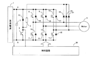
図1は、本発明のモータ制御装置の概略構成図である。図において、1はダイオード整流などの入力電源へ回生する機能のない直流電源、2は平滑コンデンサ、3は抵抗、4はモータ、5〜11は半導体スイッチ、12〜21はダイオード、30は制御回路である。なお、図において、第1乃至3の従来技術におけるモータ制御装置の図14乃至16に付された構成と同一の符号を付しているが、相互に関係するものではなく、その作用効果も全く異なるものである。
本発明における回生エネルギー処理回路またはDB回路は、抵抗3、半導体スイッチ5、ダイオード12、ダイオード19乃至21で構成されるものであり、抵抗3が両回路に共用する抵抗となるものである。
FIG. 1 is a schematic configuration diagram of a motor control device of the present invention. In the figure, 1 is a DC power supply having no function of regenerating to an input power supply such as diode rectification, 2 is a smoothing capacitor, 3 is a resistor, 4 is a motor, 5 to 11 are semiconductor switches, 12 to 21 are diodes, and 30 is a control circuit. It is. In the figure, the same reference numerals as those shown in FIGS. 14 to 16 of the motor control devices in the first to third prior arts are attached, but they are not related to each other, and their functions and effects are completely different. Is different.
The regenerative energy processing circuit or DB circuit in the present invention is composed of the
回生エネルギー処理回路またはDB回路は、モータ4と半導体スイッチ6乃至11とが繋がる出力線上にダイオード19〜21のアノードを接続し、ダイオード19〜21の全てのカソードと抵抗3とを接続する。また、抵抗3の他端は半導体スイッチ5のコレクタとダイオード12のアノードに接続され、半導体スイッチ5のエミッタは直流電源1の負端子(N)に接続され、ダイオード12のカソードは直流電源1の正端子(P)へ接続される。なお、ダイオード12は、半導体スイッチ5がオフした際に、抵抗3の配線インダクタンスに起因するサージ電圧を抑制するために必要なものである。
The regenerative energy processing circuit or the DB circuit connects the anodes of the
また、各半導体スイッチ5〜11は、制御回路30によってオンオフを制御されるものであって、制御回路30は、半導体スイッチ6〜11とダイオード13〜18で構成されるインバータブリッジを制御してモータ4を駆動する。なお、回生エネルギー処理回路またはDB回路におけるダイオード19〜21、抵抗3、半導体スイッチ5、ダイオード12には、モータ4を駆動する通常運転時に電流が流れない(制御回路30による半導体スイッチ5のオン動作をしない)ので、モータ制御装置の効率は従来に比べて低下せず、冷却装置も従来の装置と同じでよいのである。
また、制御装置30は、直流電源1のPとNの端子間電圧である主回路電圧(VPN)を監視し、適宜、半導体スイッチ5をオンオフ動作させるものである。
Each of the semiconductor switches 5 to 11 is controlled to be turned on / off by the
The
図2は本発明の回生エネルギー処理回路動作時の電流経路例を示す図であり、図3は本発明のDB回路動作時の電流経路例を示す図である。図において、図1と同一の符号を付した構成は、同一の作用効果を奏するものであるため、詳細な説明は省略する。
図2において点線矢印が回生時の電流経路であり、図1における制御回路30は、図示するように半導体スイッチ5,6,8,10をオン動作させると、平滑コンデンサ2に蓄えられたエネルギーは該電流経路を通って、抵抗3によって消費されるのである。
また、図3において点線矢印がDB時の電流経路であり、図1における制御回路30は、図示するように半導体スイッチ5のみをオン動作させると、モータ4からのDBエネルギーは該電流経路を通って、抵抗3によって消費されるのである。
このように、回生時またはDB時にオン動作させる半導体スイッチを可変することにより、抵抗3を共用できると共に、簡単な回路構成により、回生エネルギー処理回路とDB回路とを構成できるのである。
FIG. 2 is a diagram showing an example of a current path during operation of the regenerative energy processing circuit of the present invention, and FIG. 3 is a diagram showing an example of a current path during operation of the DB circuit of the present invention. In the figure, the configuration denoted by the same reference numerals as those in FIG. 1 exhibits the same operational effects, and thus detailed description thereof is omitted.
In FIG. 2, the dotted arrow indicates the current path during regeneration. When the
In FIG. 3, the dotted arrow indicates the current path during DB. When the
Thus, by changing the semiconductor switch that is turned on during regeneration or DB, the
図4は本発明の回生エネルギー処理回路動作時の各スイッチ(半導体スイッチ5〜11)動作例1を示す図であり、図5は本発明の回生エネルギー処理回路動作時の各スイッチ(半導体スイッチ5〜11)動作例2を示す図である。図において、U,V,W相電圧指令および搬送波(キャリア)は、図1における制御回路30が半導体スイッチ6乃至11をPWM制御するための信号、SW5乃至11は、図1における半導体スイッチ5乃至11に相当する各SWのオンオフ動作信号(半導体スイッチ5乃至11がIGBTやnチャンネルMOSFETの場合、ゲート電圧信号に相当)、DB制御信号および回生制御信号は、図1における制御回路30がある条件下で発生する信号、主回路電圧は、図1における直流電源1のP(正)とN(負)の端子間電圧であり、制御回路30がこの主回路電圧を監視するものである。
FIG. 4 is a diagram showing an operation example 1 of each switch (semiconductor switches 5 to 11) when the regenerative energy processing circuit of the present invention is operated, and FIG. 5 is a diagram showing each switch (semiconductor switch 5) when the regenerative energy processing circuit of the present invention is operated. FIG. 11 is a diagram illustrating an operation example 2; In the figure, U, V, and W phase voltage commands and carrier waves are signals for the
インバータブリッジ(図1における半導体スイッチ6乃至11およびダイオード13乃至18に相当)が、図4のようにPWM動作を行っている場合、回生動作時、即ちモータ4からの回生エネルギーがモータ制御装置側に移動すると、直流電源1は電源回生機能がないので、回生エネルギーは平滑コンデンサ3へ蓄えられ主回路電圧が上昇する。
しかしながら、PWM動作の中で、半導体スイッチ6、8、10がオン、半導体スイッチ7、9、11がオフであって、インバータブリッジの全ての出力電圧が直流電源1のP(正)の端子電圧となり、モータ4へ印加される線間電圧は零となる状態(線間出力零電圧状態)、または、半導体スイッチ6、8、10がオフ、半導体スイッチ7、9、11がオンであって、インバータブリッジの全ての出力電圧が直流電源1のN(負)の端子電圧となり、モータ4へ印加される線間電圧は零となる状態(線間出力零電圧状態)では、電流はモータ4の配線内で閉じてしまうので、平滑コンデンサ3への充電は行われないのである。
When the inverter bridge (corresponding to the semiconductor switches 6 to 11 and the
However, in the PWM operation, the semiconductor switches 6, 8, 10 are on, the semiconductor switches 7, 9, 11 are off, and all the output voltages of the inverter bridge are the P (positive) terminal voltage of the
ここで、主回路電圧がON Levelに達すると、制御回路30は回生制御信号をオンとし、回生制御信号とSW6、SW8、SW10の信号とが、全てオンとなる線間出力零電圧状態のタイミングで、SW5をオンとして半導体スイッチ5をオン動作させる。このようにすると、平滑コンデンサ2に蓄えられたエネルギーは、図2のような電流経路を通って、抵抗3によって消費され、これに伴って、主回路電圧が低下し、OFF Levelに達すると、制御回路30は回生制御信号をオフとし、SW5をオフとして半導体スイッチ5をオフ動作させる。なお、ON LevelとOFF Levelは、平滑コンデンサ2など主回路電圧が印加される部品が破壊しないレベルの電位を選べばよい。
Here, when the main circuit voltage reaches ON Level, the
このようなPWM動作中の回生エネルギーの移動は、図4に示す通り、インバータブリッジが線間出力零電圧状態でない時は、モータからモータ制御装置側へ回生エネルギーが移動し平滑コンデンサの電圧が上昇する。一方、線間出力零電圧状態では、モータの回生エネルギーはモータ内で閉じており外部へは出力されない。
前述のように、半導体スイッチ6、8、10がオンの線間出力零電圧状態で半導体スイッチ5がオンすると、主回路の平滑コンデンサに蓄えられたエネルギーは、抵抗に移動し消費される。このとき半導体スイッチ6、8、10には、モータの負荷電流方向によって、モータの電流と平滑コンデンサから抵抗へ流れる電流の和が流れることとなり、半導体スイッチの損失が従来のモータ制御装置よりも増加することもある。しかしながら、回生エネルギー処理は、もともとエネルギーを抵抗の損失へ変えるものであるので、この動作時に損失が増えることはモータ制御装置の効率には影響なく問題ないものである。なお、この電流増加に伴う損失増加が、半導体スイッチ5、6、8、10の冷却能力を超えないように抵抗3の値を決めるか、駆動する負荷側で回生エネルギー量を制限する必要がある。
When the inverter bridge is not in the line output zero voltage state, the regenerative energy moves from the motor to the motor controller side and the voltage of the smoothing capacitor rises as shown in FIG. To do. On the other hand, in the line output zero voltage state, the regenerative energy of the motor is closed in the motor and is not output to the outside.
As described above, when the
図4に示す例は、PWM周期中(搬送波の山から山の間)に、主回路電圧が、一旦ON Levelを超えて、回生エネルギー処理によりOFF Levelまで低下した例であるが、回生エネルギーと抵抗3で消費できるエネルギーとのバランスから、図5のように複数のPWM周期に渡って回生エネルギー処理が継続することもある。
The example shown in FIG. 4 is an example in which, during the PWM period (between the peaks of the carrier wave), the main circuit voltage once exceeds ON Level and is reduced to OFF Level by regenerative energy processing. From the balance with the energy that can be consumed by the
図6は本発明の回生エネルギー処理回路動作比率を増加させた動作例を示す図であり、図7は本発明の回生エネルギー処理回路動作比率を調整させた動作例を示す図である。図において、図4および5と同一の信号名の記載は、同一の作用をするものであるため、詳細な説明は省略する。
前述のように、抵抗3による回生エネルギー処理動作は、半導体スイッチ6、8、10が全てオンとなる線間出力零電圧状態の条件下のみで行われる。この線間出力零電圧状態の期間は、インバータブリッジの出力電圧に依存し、出力電圧が高い場合は、この期間が非常に短くなる。モータ4から電力を回生する条件では、インバータ出力電圧 < モータ電圧(モータの電圧はモータ回転速度に依存)となるため、線間出力零電圧の期間は、ある程度確保される傾向になる。
FIG. 6 is a diagram showing an operation example in which the regenerative energy processing circuit operation ratio of the present invention is increased, and FIG. 7 is a diagram showing an operation example in which the regenerative energy processing circuit operation ratio of the present invention is adjusted. In the figure, the description of the same signal name as in FIGS. 4 and 5 has the same function, and thus detailed description thereof is omitted.
As described above, the regenerative energy processing operation by the
一旦ON Levelを超えた主回路電圧を早く減少させる必要がある場合は、図6のように、半導体スイッチ6、8、10が全てオンとなる線間出力零電圧状態の期間を長くすればよい。即ち、3相の電圧指令(U,V,W相電圧指令)に同じ量のオフセット量を加えることにより、半導体スイッチ6、8、10が全てオンとなる線間出力零電圧状態の期間を長くすることができる。3相の電圧指令(U,V,W相電圧指令)に同じ量のオフセット量を加えるということは、半導体スイッチ7、9、11が全てオンとなる線間出力零電圧状態の期間を短くし、半導体スイッチ6、8、10が全てオンとなる線間出力零電圧状態の期間を長くするように調整し、一旦ON Levelを超えた主回路電圧を早く減少させるのである。なお、この場合、モータ4の端子間電圧(線間電圧)は変化しないので、モータ4の駆動・回生にはなんら影響なく、回生エネルギーの消費を多く行うことができるのである。また、この期間の調整(3相の電圧指令(U,V,W相電圧指令)に同じ量のオフセット量を加える調整)は、図7のように必要な時にのみ行い、必要ない場合は従来の期間へ戻してもよいものである。
When it is necessary to quickly reduce the main circuit voltage once exceeding the ON level, the period of the line output zero voltage state in which the semiconductor switches 6, 8, and 10 are all turned on may be lengthened as shown in FIG. . That is, by adding the same amount of offset to the three-phase voltage command (U, V, W-phase voltage command), the period of the line output zero voltage state in which the semiconductor switches 6, 8, 10 are all turned on is lengthened. can do. Adding the same amount of offset to the three-phase voltage command (U, V, W-phase voltage command) shortens the period of the line output zero voltage state in which the semiconductor switches 7, 9, and 11 are all turned on. Then, adjustment is made to lengthen the period of the line output zero voltage state in which all the semiconductor switches 6, 8, and 10 are turned on, and the main circuit voltage that once exceeds the ON level is quickly reduced. In this case, the inter-terminal voltage (line voltage) of the
図8は、本発明のDB動作時の各スイッチ動作例を示す図である。図において、図4乃至7と同一の信号名の記載は、同一の作用をするものであるため、詳細な説明は省略する。
本発明におけるモータ制御装置のダイナミックブレーキ動作は、図1における制御回路30が入力電源の停電、装置故障などを監視して、ダイナミックブレーキを用いた非常停止の必要性を判断した上で行うものである。
ダイナミックブレーキを行う場合には、制御回路は、DB制御信号をオン、かつ半導体スイッチ6〜11の信号SW6〜SW11の全てをオフとし、半導体スイッチ5の信号SW5をオンとして半導体スイッチ5をオン動作させる。この時のDB時の電流経路は、図3の例に示すような経路を通って、電力が抵抗3によって消費されるのである。
FIG. 8 is a diagram showing an example of each switch operation during the DB operation of the present invention. In the figure, the description of the same signal name as in FIGS. 4 to 7 has the same function, and thus the detailed description is omitted.
The dynamic brake operation of the motor control device according to the present invention is performed after the
When performing dynamic braking, the control circuit turns on the DB control signal, turns off all of the signals SW6 to SW11 of the semiconductor switches 6 to 11, turns on the signal SW5 of the
図9は、本発明の回生エネルギー処理回路動作からDB動作へ移行する動作例を示す図である。図において、図4乃至8と同一の信号名の記載は、同一の作用をするものであるため、詳細な説明は省略する。
前述のように、ダイナミックブレーキを行うと、モータからのエネルギーは図3に示すDB時の電流経路を介して電力が抵抗3で消費されるので、主回路電圧を下げることはできなくなる。しかしながら、モータから平滑コンデンサ2への充電がなくなるので、平滑コンデンサの電位上昇も止まり、主回路電圧がON Level以下であれば、平滑コンデンサ2等の部品の電圧破壊もないため、この電圧で保持されても問題はない。
したがって、回生エネルギー処理回路動作からDB動作へ移行する場合においても、主回路電圧がON Level以下であれば、ダイナミックブレーキを行っても何ら問題はないのである。逆に、回生エネルギー処理回路動作中の主回路電圧がON Level以上である間は、ダイナミックブレーキを行わない等のシーケンス処理か、負荷装置の保護を優先する場合はダイナミックブレーキを行い、ON Levelの値を若干超える値も平滑コンデンサ2など主回路電圧が印加される部品が破壊しないレベルに設計することが必要である。
FIG. 9 is a diagram showing an operation example of transition from the regenerative energy processing circuit operation of the present invention to the DB operation. In the figure, the description of the same signal name as in FIGS. 4 to 8 has the same function, and thus detailed description is omitted.
As described above, when dynamic braking is performed, energy from the motor is consumed by the
Therefore, even when transitioning from the regenerative energy processing circuit operation to the DB operation, if the main circuit voltage is equal to or less than ON Level, there is no problem even if dynamic braking is performed. Conversely, while the main circuit voltage during operation of the regenerative energy processing circuit is equal to or higher than ON Level, sequence processing such as dynamic braking is not performed, or if priority is given to protection of the load device, dynamic braking is performed, and ON Level A value slightly exceeding the value must be designed to a level that does not destroy the parts to which the main circuit voltage is applied, such as the smoothing
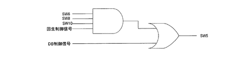
図10 は、本発明のSW5の動作信号を生成するロジック回路例を示す図であって、図4乃至9におけるSW6,8,10の動作信号および回生制御信号ならびにDB制御信号からSW5の動作信号を作り出すロジック回路の例である。このような簡単なロジック回路での構成が可能であり、モータ制御装置として安価に実現可能なものである。 FIG. 10 is a diagram showing an example of a logic circuit that generates the operation signal of SW5 of the present invention. The operation signal of SW5 from SW6, 8, and 10 and the regeneration control signal and the DB control signal in FIGS. This is an example of a logic circuit that generates A configuration with such a simple logic circuit is possible, and the motor control device can be realized at low cost.
図11(a)は本発明の抵抗回路を増加させる場合の実施例を示す図、(b)は本発明の抵抗回路を増加させる場合の他の実施例を示す図である。図において、27は半導体スイッチ、28は抵抗、29はダイオードであって、図1乃至3と同一の符号を付した構成は、同一の作用効果を奏するものであるため、詳細な説明は省略する。
回生エネルギーの消費電力とダイナミックブレーキの消費電力は、モータ制御装置が利用される負荷装置の容量や、その運転条件によって決まるので、その条件に応じて、それぞれ違う最適値が存在することが知られている。
回生エネルギーは負荷に依存するものであって、モータ制御装置の数〜数十%程度であり、モータ制御装置の利用時にその抵抗値R1が設計される。また、ダイナミックブレーキは、モータの巻線インダクタンスと巻線抵抗、回転数によって、最短時間で停止する抵抗値の最適値R2が決まるので、モータ固有の値となる。
FIG. 11A is a diagram showing an embodiment when the resistance circuit of the present invention is increased, and FIG. 11B is a diagram showing another embodiment when the resistance circuit of the present invention is increased. In the figure, reference numeral 27 denotes a semiconductor switch, 28 denotes a resistor, and 29 denotes a diode. The configurations denoted by the same reference numerals as those in FIGS. 1 to 3 have the same operational effects, and thus detailed description thereof is omitted. .
Since the power consumption of regenerative energy and the power consumption of dynamic brake are determined by the capacity of the load device used by the motor control device and its operating conditions, it is known that there are different optimum values depending on the conditions. ing.
The regenerative energy depends on the load and is about several to several tens of percent of the motor control device, and the resistance value R1 is designed when the motor control device is used. In addition, the dynamic brake has a motor-specific value because the optimum resistance value R2 for stopping in the shortest time is determined by the winding inductance, winding resistance, and rotation speed of the motor.
一般的には、ダイナミックブレーキに最適な抵抗値R2は低めの値で、R1>R2である。本発明のモータ制御装置のように、回生エネルギー処理回路とDB回路との抵抗を共用すると、回生時の抵抗はパルス動作となるので、単位時間当たりの抵抗利用率をD(<1.0)、抵抗値をR2とすると、等価的な回生用の抵抗値はR1=R2/Dとなり、R1>R2の条件を満たす。
したがって、抵抗の容量は、一般的に回生用抵抗の方が大きいので、抵抗サイズは必要な回生エネルギー消費量に合わせるように設計すればよい。
In general, the optimum resistance value R2 for the dynamic brake is a low value, and R1> R2. When the resistance of the regenerative energy processing circuit and the DB circuit is shared as in the motor control device of the present invention, the resistance at the time of regeneration is a pulse operation, so the resistance utilization rate per unit time is D (<1.0). When the resistance value is R2, the equivalent regenerative resistance value is R1 = R2 / D, which satisfies the condition of R1> R2.
Therefore, the capacity of the resistor is generally larger for the regenerative resistor, and the resistor size may be designed to match the required amount of regenerative energy consumption.
また、回生用の抵抗とダイナミックブレーキ用の抵抗とを分けて設計したい場合や、抵抗値を状況に応じて細かく調整したい場合には、図11(a)(b)のように、半導体スイッチ27と抵抗28、ダイオード29を増やし、抵抗3と抵抗4を直列または並列接続することで、各動作の抵抗値を変更し、最適値に近づけることができる。
なお、図11は抵抗回路を1つ増設する例を示したが、増設数をさらに増やしてもよい。また、抵抗を多数並列接続するよう構成すれば、各抵抗の有効あるいは無効の組み合わせにより、細かい抵抗値の調整が可能となり、ブレーキ時の力の可変もできるようになる。
Further, when it is desired to design the regenerative resistor and the dynamic brake resistor separately, or when it is desired to finely adjust the resistance value according to the situation, the semiconductor switch 27 is used as shown in FIGS. Further, the
Although FIG. 11 shows an example in which one resistor circuit is added, the number of extensions may be further increased. In addition, if a large number of resistors are connected in parallel, the resistance value can be finely adjusted and the force at the time of braking can be varied depending on whether the resistors are valid or invalid.
1 直流電源
2 平滑コンデンサ
3、25、28 抵抗
4 モータ
5〜11、27 半導体スイッチ
12〜21、29 ダイオード
30 制御回路
DESCRIPTION OF
Claims (11)
前記直流電源の正側負側間に接続する平滑コンデンサと、
前記直流電源からの直流電力を交流電力に変換してモータへ供給するインバータブリッジを含むインバータブリッジ回路と、
前記インバータブリッジ回路にPWM制御信号を出力する制御回路と、
前記インバータブリッジの出力端それぞれにアノード端子を個別に接続する複数のダイオードと、
複数の前記ダイオードのカソード端子をコモン接続すると共に、該コモン端子とその一端とを接続する共通抵抗と、
前記共通抵抗の他端とその一端とを接続すると共に、前記直流電源の負側とその他端とを接続する半導体スイッチと、
前記半導体スイッチの一端とアノード端子とを接続すると共に、前記直流電源の正側とカソード端子とを接続する他のダイオードと、を備えたことを特徴とするモータ制御装置。 DC power supply,
A smoothing capacitor connected between the positive and negative sides of the DC power supply ;
An inverter bridge circuit including an inverter bridge that converts DC power from the DC power source into AC power and supplies the motor to the motor ;
A control circuit for outputting a PWM control signal to the inverter bridge circuit;
A plurality of diodes individually connecting anode terminals to the output ends of the inverter bridge;
Commonly connecting the cathode terminals of the plurality of diodes, and a common resistor connecting the common terminal and one end thereof,
A semiconductor switch for connecting the other end of the common resistor and one end thereof, and connecting a negative side of the DC power source and the other end;
A motor control device comprising: another diode for connecting one end of the semiconductor switch and an anode terminal, and for connecting a positive side of the DC power source and a cathode terminal .
回生の場合、前記インバータブリッジの出力電圧が、全て、前記直流電源の正側電圧となる前記PWM制御信号のタイミング時に、前記半導体スイッチをオン動作させることを特徴とする請求項1または2に記載のモータ制御装置。 When the control circuit is a dynamic brake, all the inverter bridges are turned off, and the semiconductor switch is turned on.
3. The semiconductor switch according to claim 1 , wherein in the case of regeneration, the semiconductor switch is turned on at the timing of the PWM control signal in which all the output voltages of the inverter bridge become the positive side voltage of the DC power supply. the motor controller.
回生の場合、前記インバータブリッジから前記モータに印加される線間電圧がゼロ状態となる前記PWM制御信号のタイミング時に、前記半導体スイッチをオン動作させることを特徴とする請求項1または2に記載のモータ制御装置。3. The semiconductor switch according to claim 1, wherein in the case of regeneration, the semiconductor switch is turned on at a timing of the PWM control signal at which a line voltage applied from the inverter bridge to the motor becomes zero. Motor control device.
11. The control circuit according to claim 10, wherein the control circuit varies the time of the PWM control signal during a PWM cycle by adding an offset amount to a voltage command for generating the PWM control signal. Motor control device.
Priority Applications (1)
| Application Number | Priority Date | Filing Date | Title |
|---|---|---|---|
| JP2008291921A JP5049251B2 (en) | 2008-11-14 | 2008-11-14 | Motor control device |
Applications Claiming Priority (1)
| Application Number | Priority Date | Filing Date | Title |
|---|---|---|---|
| JP2008291921A JP5049251B2 (en) | 2008-11-14 | 2008-11-14 | Motor control device |
Related Child Applications (1)
| Application Number | Title | Priority Date | Filing Date |
|---|---|---|---|
| JP2012161887A Division JP2012196143A (en) | 2012-07-20 | 2012-07-20 | Motor control device |
Publications (3)
| Publication Number | Publication Date |
|---|---|
| JP2010119253A JP2010119253A (en) | 2010-05-27 |
| JP2010119253A5 JP2010119253A5 (en) | 2011-10-20 |
| JP5049251B2 true JP5049251B2 (en) | 2012-10-17 |
Family
ID=42306519
Family Applications (1)
| Application Number | Title | Priority Date | Filing Date |
|---|---|---|---|
| JP2008291921A Expired - Fee Related JP5049251B2 (en) | 2008-11-14 | 2008-11-14 | Motor control device |
Country Status (1)
| Country | Link |
|---|---|
| JP (1) | JP5049251B2 (en) |
Families Citing this family (4)
| Publication number | Priority date | Publication date | Assignee | Title |
|---|---|---|---|---|
| CN104583105A (en) * | 2012-08-22 | 2015-04-29 | 奥的斯电梯公司 | Elevator system using dynamic braking |
| JP5918406B1 (en) * | 2015-02-19 | 2016-05-18 | 株式会社荏原製作所 | Dry vacuum pump device and control method thereof |
| JP7002522B2 (en) * | 2019-12-13 | 2022-01-20 | シナノケンシ株式会社 | Motor drive |
| CN113765438A (en) * | 2020-06-01 | 2021-12-07 | 施耐德电器工业公司 | Brake control circuit, motor brake control method and system |
-
2008
- 2008-11-14 JP JP2008291921A patent/JP5049251B2/en not_active Expired - Fee Related
Also Published As
| Publication number | Publication date |
|---|---|
| JP2010119253A (en) | 2010-05-27 |
Similar Documents
| Publication | Publication Date | Title |
|---|---|---|
| JP2012196143A (en) | Motor control device | |
| JP6285477B2 (en) | Motor drive device having dynamic brake circuit protection function | |
| JP4939570B2 (en) | Power supply | |
| JP5716715B2 (en) | Rotating electric machine for vehicles | |
| JP6183460B2 (en) | Inverter device | |
| JP5641448B2 (en) | Rotating electric machine for vehicles | |
| US20090230898A1 (en) | Servo amplifier with regenerative function | |
| JP6469894B2 (en) | Power converter | |
| JP2016073127A (en) | Inverter controller, electric power converter and electric vehicle | |
| JP6944546B2 (en) | Power converter | |
| JP5049251B2 (en) | Motor control device | |
| JP6150017B2 (en) | Driving device, matrix converter and elevator system | |
| JP7424407B2 (en) | Control devices, motor drive devices and motor drive systems | |
| JP2008017649A (en) | Overcurrent detection circuit | |
| JP6119531B2 (en) | Rotating electric machine for vehicles | |
| WO2022158052A1 (en) | Gate drive circuit and power conversion device | |
| JP7421435B2 (en) | Motor control device and motor control method | |
| WO2019167427A1 (en) | Motor drive control device and motor drive control method | |
| WO2023187863A1 (en) | Driving circuit and control method for driving circuit | |
| JP5268819B2 (en) | Motor control device | |
| JP2021114851A (en) | Motor driver, motor driver control circuit, and motor driver control method | |
| JP2016226234A (en) | Inverter controller, power conversion device, and vehicle | |
| JP2006094654A (en) | Power conversion apparatus using gate control method of self arc-method for controlling gate of self arc-extinguishing type device connected in multiple series, and power conversion device using this method | |
| JP5313493B2 (en) | Motor drive device | |
| JP2021044994A (en) | Actuator and actuator system |
Legal Events
| Date | Code | Title | Description |
|---|---|---|---|
| A621 | Written request for application examination |
Free format text: JAPANESE INTERMEDIATE CODE: A621 Effective date: 20100614 |
|
| A521 | Written amendment |
Free format text: JAPANESE INTERMEDIATE CODE: A523 Effective date: 20110907 |
|
| RD02 | Notification of acceptance of power of attorney |
Free format text: JAPANESE INTERMEDIATE CODE: A7422 Effective date: 20120216 |
|
| A977 | Report on retrieval |
Free format text: JAPANESE INTERMEDIATE CODE: A971007 Effective date: 20120606 |
|
| TRDD | Decision of grant or rejection written | ||
| A01 | Written decision to grant a patent or to grant a registration (utility model) |
Free format text: JAPANESE INTERMEDIATE CODE: A01 Effective date: 20120626 |
|
| A01 | Written decision to grant a patent or to grant a registration (utility model) |
Free format text: JAPANESE INTERMEDIATE CODE: A01 |
|
| A61 | First payment of annual fees (during grant procedure) |
Free format text: JAPANESE INTERMEDIATE CODE: A61 Effective date: 20120720 |
|
| FPAY | Renewal fee payment (prs date is renewal date of database) |
Free format text: PAYMENT UNTIL: 20150727 Year of fee payment: 3 |
|
| R150 | Certificate of patent (=grant) or registration of utility model |
Free format text: JAPANESE INTERMEDIATE CODE: R150 |
|
| LAPS | Cancellation because of no payment of annual fees |