JP5048836B2 - A method for compressing and correlating valing in graphics systems - Google Patents
A method for compressing and correlating valing in graphics systems Download PDFInfo
- Publication number
- JP5048836B2 JP5048836B2 JP2010520164A JP2010520164A JP5048836B2 JP 5048836 B2 JP5048836 B2 JP 5048836B2 JP 2010520164 A JP2010520164 A JP 2010520164A JP 2010520164 A JP2010520164 A JP 2010520164A JP 5048836 B2 JP5048836 B2 JP 5048836B2
- Authority
- JP
- Japan
- Prior art keywords
- shader
- register
- shared
- vertex
- input
- Prior art date
- Legal status (The legal status is an assumption and is not a legal conclusion. Google has not performed a legal analysis and makes no representation as to the accuracy of the status listed.)
- Expired - Fee Related
Links
Images


Classifications
-
- G—PHYSICS
- G06—COMPUTING; CALCULATING OR COUNTING
- G06T—IMAGE DATA PROCESSING OR GENERATION, IN GENERAL
- G06T1/00—General purpose image data processing
- G06T1/60—Memory management
-
- G—PHYSICS
- G06—COMPUTING; CALCULATING OR COUNTING
- G06T—IMAGE DATA PROCESSING OR GENERATION, IN GENERAL
- G06T15/00—3D [Three Dimensional] image rendering
- G06T15/005—General purpose rendering architectures
Landscapes
- Engineering & Computer Science (AREA)
- Physics & Mathematics (AREA)
- General Physics & Mathematics (AREA)
- Theoretical Computer Science (AREA)
- Computer Graphics (AREA)
- Image Generation (AREA)
- Devices For Executing Special Programs (AREA)
- Memory System Of A Hierarchy Structure (AREA)
- Complex Calculations (AREA)
Description
本開示は、一般にグラフィックス処理に、さらに詳細には、グラフィック・システムにおけるヴァリング(varying)の圧縮(packing)および関連付け(linking)のための技術に関連する。 The present disclosure, in general, graphics processing, and more particularly relates to techniques for compressing the Varingu (Varying) in the graphics system (packing) and association (linking).
公のグラフィック標準、OpenGLまたはOpenGL ESは、頂点およびフラグメント・シェーダを使用する、頂点ごとのおよび画素ごとの操作の時に、変化させ得る固定された機能を持つ。頂点およびフラグメント・シェーダは、標準のOpenGL機能により達成されていない特殊な効果を与えるために開発されている。 The public graphics standard, OpenGL or OpenGL ES, has fixed functions that can be changed during per-vertex and per-pixel operations using vertex and fragment shaders. Vertex and fragment shaders have been developed to give special effects not achieved by standard OpenGL functionality.
ここで図1を参照すると、シェーダを含むグラフィックス処理ユニット(GPU)における、従来のパイプライン・ステージの一般的なフローチャートが示される。そこには、3つの主要なパイプライン・ステージ、ブロックS10で示される頂点シェーダ、ブロックS12で示されるプリィミティブ・アセンブラとラスタライザ、およびS14で示されるフラグメント・シェーダがある。さらなるブロックS16は、サンプルごとの操作のために提供される。 Referring now to FIG. 1, a general flowchart of a conventional pipeline stage in a graphics processing unit (GPU) that includes a shader is shown. There are three main pipeline stages, a vertex shader indicated by block S10, a primitive assembler and rasterizer indicated by block S12, and a fragment shader indicated by S14. A further block S16 is provided for sample-by-sample operation.
頂点シェーダ(vertex shader:VS)S10は、幾何学的な物体の各々の頂点のために実行される、プログラムまたはコンピュータ・プログラム製品である。VS S10の入力は、属性と呼ばれ、ブロックA2に示される。VS S10はまた、入力として、いくつかの頂点ユニフォーム0〜95(すなわち96個の頂点ユニフォーム)を含むことができる、頂点ユニフォームVU2を受け取る。VS S10から、および、その時の、プリィミティブ・アセンブラおよびラスタライザ(rasterizer)S12からの出力は、ブロックV3に示されるように、一般にヴァリング(varyings)として呼ばれ、一般に、(VS出力を記憶する)頂点キャッシュ、または、(ラスタライザの出力を記憶する)他の記憶メディアの中に存在する。ヴァリングV3は、幾何学的な物体の三角形のピクセルに関連付けられた値であり得る。画素に関連付けられた値は、幾何学的な物体の三角形頂点に関連付されたVSの結果に基づいて計算された、プリィミティブ・アセンブラおよびラスタライザS12の結果である。頂点に関連するVSの結果および画素に関連するヴァリングV3は、同じ名前またはID、型式と順序を持つ。画素に関連するヴァリングV3は、フラグメント・シェーダ(FS)S14への入力である。FS S14は、また、一般に、いくつかの(例えば16個の)フラグメント・ユニフォームを含む、フラグメント・ユニフォームFU3を入力として受け取る。 A vertex shader (VS) S10 is a program or computer program product that is executed for each vertex of a geometric object. The input of VS S10 is called an attribute and is shown in block A2. VS S10 also receives as input vertex vertex uniform VU2, which may include several vertex uniforms 0-95 (ie, 96 vertex uniforms). The output from VS S10 and at that time from the primitive assembler and rasterizer S12 is commonly referred to as varyings , as shown in block V3, and is generally the vertex (which stores the VS output). It resides in a cache or other storage medium (which stores the output of the rasterizer). Varing V3 may be a value associated with a triangular pixel of a geometric object. The value associated with the pixel is the result of the primitive assembler and rasterizer S12 calculated based on the VS result associated with the triangle vertices of the geometric object. The VS result associated with the vertex and the Valing V3 associated with the pixel have the same name or ID, type and order. Varing V3 associated with the pixel is an input to the fragment shader (FS) S14. The FS S14 also receives as input a fragment uniform FU3, which typically includes several (eg 16) fragment uniforms.
図2は、シェーダを含む、従来のパイプライン・ステージの一般的なブロック・ダイアグラムを示す。グラフィックス処理装置(GPU)内のVS S510のために、そこには、属性0〜7を記憶するために、一般に、8個の属性レジスタRA2がある。一般に、そこに、ヴァリング(varyings)0〜7を記憶するために、8個の出力ヴァリングレジスタRV3Aがある。ヴァリングレジスタRV3Aは、通常の場合には頂点キャッシュであり、VS出力を記憶する。そこには、一般に、ヴァリング0〜7を記憶するために、8個の出力ヴァリングレジスタRV3Bがある。ヴァリングレジスタRV3Bは、画素に関連するヴァリング(varyings)に対応する、ラスタライザの結果を記憶する。属性レジスタRA2とヴァリングレジスタRV3Aは、それぞれ、属性0〜7にインデックスをつけられた、入力レジスタと、ヴァリング0〜7にインデックスをつけられた出力ヴァリングレジスタである。これらのレジスタIDは、高級言語からマシン言語に、頂点シェーダとフラグメント・シェーダのプログラムをコンパイルする、コンパイラによって割り当てられる。高級言語における、シェーダ・プログラムで使用されるレジスタは、ID/インデックスの代わりに、名前により名づけられる。レジスタの名前は、アプリケーション開発者からだけ、見ることができる。アプリケーションは、レジスタの名前により、レジスタをアクセスする。レジスタのIDは、GPUハードウェア(HW)において、VS S10またはFS S14によってのみ、見ることができる。したがって、VS入力シンボル・テーブル、出力シンボル・テーブルおよび入力シンボル・テーブルのような、シンボル・テーブルはコンパイラによって生成されるであろう。しかしながら、VS入力または入力シンボル・テーブルは、内容、IDおよび名前に関して、出力または出力シンボル・テーブルとは関係を持たない。 FIG. 2 shows a general block diagram of a conventional pipeline stage including a shader. For VS S510 in the graphics processing unit (GPU), there are generally eight attribute registers RA2 for storing attributes 0-7. Generally, there, to store Varingu (varyings) 0 to 7, there are eight output Varingu register RV3A. The Valing register RV3A is a vertex cache in a normal case and stores a VS output. There are, generally, to store Varingu 0-7, there are eight output Varingu register RV3B. Varingu register RV3B corresponds to Varingu (varyings) associated with the pixel, storing the results of the rasterizer. Attribute register RA2 and Varingu register RV3A were each indexed to attribute 0-7, an input register, an output Varingu register indexed to Varingu 0-7. These register IDs are assigned from a high-level language to a machine language by a compiler that compiles vertex shader and fragment shader programs. Registers used in shader programs in high-level languages are named by name instead of ID / index. Register names are only visible to application developers. An application accesses a register by the name of the register. The register ID can only be seen in the GPU hardware (HW) by VS S10 or FS S14. Thus, symbol tables such as the VS input symbol table, output symbol table, and input symbol table will be generated by the compiler. However, the VS input or input symbol table has nothing to do with the output or output symbol table in terms of content, ID and name.
FS S14の入力または入力シンボル・テーブルは、VS S10の出力または出力シンボル・テーブルのサブセットであり得るかもしれないが、VS出力または出力シンボル・テーブルは、内容および名前の点で、FS S14の入力または入力シンボル・テーブルと一致しなければならない。 The input or input symbol table of FS S14 may be a subset of the output or output symbol table of VS S10, but the VS output or output symbol table is the input of FS S14 in terms of content and name. Or must match the input symbol table.
VS S10は、また、T2として示されているテクスチャ、および、TV2として示されている一時変数と同様に、記憶媒体に記憶されている頂点ユニフォームVU2を、入力として受け取る。プリィミティブ・アセンブラとラスタライザS12は、ヴァリング0〜7とパラメータgl_Position Pによってインデックスをつけられた、出力ヴァリングレジスタRV3A内のヴァリングを受け取る。プリィミティブ・アセンブラとラスタライザS12は、ヴァリング0〜7とgl_Position Pによってインデックスをつけられた、出力ヴァリングレジスタRV3Bにヴァリングを出力する。FS S14は、T3として示されているテクスチャと、TV3として示されている一時変数と同様に、記憶メディアに記憶されている、フラグメント・ユニフォームを入力として受け取る。FS S14は、ヴァリング0〜7、および、Pとして示されているパラメータgl_Position Pによってインデックスをつけられた、出力ヴァリングレジスタRV3B内のヴァリングを受け取る。FS S14は、また、追加のパラメータ、gl_Fontfacing、および、PPとして示されている、gl_PointPositionを受け取る。FS S14は、gl_FragColor FCを出力する。属性(attributes)とヴァリング(varyings)は、また、シェーダ変数とも呼ばれる。 VS S10 also receives as input the texture shown as T2 and the vertex uniform VU2 stored in the storage medium, as well as the temporary variable shown as TV2. Puryimitibu assembler and rasterizer S12, was indexed by Varingu 0-7 and parameter Gl_Position P, receive Varingu in the output Varingu register RV3A. Puryimitibu assembler and rasterizer S12, was indexed by Varingu 0-7 and Gl_Position P, and outputs the Varingu output Varingu register RV3B. The FS S14 receives as input the fragment uniform stored in the storage medium, as well as the texture shown as T3 and the temporary variable shown as TV3. FS S14 is Varingu 0-7, and were indexed by a parameter Gl_Position P, shown as P, receive Varingu in the output Varingu register RV3B. FS S14 also receives additional parameters, gl_Fontfacing, and gl_PointPosition, shown as PP. The FS S14 outputs gl_FragColor FC. Attributes and varyings are also called shader variables.
グラフィック・パイプラインにおける、ヴァリング(varying)の圧縮(packing)および関連付け(linking)の技術が、ここに説明される。シェーダ変数の圧縮は、記憶装置またはメモリがより効率的に使用されるために、モバイルのGPUにおいて有益である。シェーダ変数の圧縮は、また、トラフィックのバンド幅を減少し、電力を節約し、性能を改善し得る。 Techniques for variableing packing and linking in a graphic pipeline are described herein. Shader variable compression is beneficial in mobile GPUs because storage or memory is used more efficiently. Shader variable compression may also reduce traffic bandwidth, conserve power, and improve performance.
1つの構成において、デバイスは、複数個の共有M次元(M-dimensional:MD)レジスタを持つ、記憶媒体を含む。デバイスは、また、成分(component)の合計がMである、1つ以上のシェーダ変数を、各々の共有MDレジスタに圧縮する、1組の操作を実装するために、処理ユニットを含む。 In one configuration, the device includes a storage medium having a plurality of shared M-dimensional (MD) registers. The device also includes a processing unit to implement a set of operations that compress one or more shader variables whose total component is M into each shared MD register.
別の構成において、集積回路は、複数個の共有M次元(MD)レジスタを持つ、記憶媒体を含む。集積回路は、また、成分の合計がMである、1つ以上のシェーダ変数を、各々の共有MDレジスタに圧縮する1組の操作を実装するために、処理ユニットを含む。 In another configuration, an integrated circuit includes a storage medium having a plurality of shared M-dimensional (MD) registers. The integrated circuit also includes a processing unit to implement a set of operations that compress one or more shader variables whose sum of components is M into each shared MD register.
別の構成は、コンピュータ・プログラム製品を含む。コンピュータ・プログラム製品は、複数個のMDベクトル・レジスタの各々の共有M次元(MD)ベクトル・レジスタ内へと、成分の和がMである、1組のシェーダ変数のうちの1つ以上のシェーダ変数を、コンピュータに圧縮させる命令を含む、コンピュータ可読媒体を含む。 Another configuration includes a computer program product. The computer program product includes one or more shaders of a set of shader variables whose sum is M into each shared M-dimensional (MD) vector register of a plurality of MD vector registers. A computer readable medium containing instructions that cause the computer to compress the variables.
さらなる構成は、複数個の共有M次元(MD)レジスタを有する記憶媒体を備えるプロセッサを含んでいる。プロセッサは、また、各々の共有MDレジスタに、成分の和がMと等しい、1つ以上の共有変数を圧縮する1組の操作を実装する集積回路を含む。 A further arrangement includes a processor comprising a storage medium having a plurality of shared M-dimensional (MD) registers. The processor also includes an integrated circuit that implements in each shared MD register a set of operations that compress one or more shared variables whose sum of components is equal to M.
特に、添付された図と共に扱うことにより、追加の態様は、詳細な説明からより容易に明白になるであろう。 Additional aspects will become more readily apparent from the detailed description, particularly when taken in conjunction with the accompanying figures.
開示の態様と構成は、同じ参照文字が全体にわたって対応を識別する図と結び付けることにより、以下に示される詳細な説明から、さらに明白になるであろう。 Aspects and configurations of the disclosure will become more apparent from the detailed description set forth below when taken in conjunction with the drawings in which the same reference characters identify correspondingly throughout.
図におけるイメージは、説明の目的のために、単純化されていて、一定の縮尺で描かれていない。理解を容易にするために、そのような要素を差別化するために、適切な場合には、接尾辞が付加されても良い場合を除いて、図において共通である同一の要素を示すために、可能な場合には、同一の参照数字が使用されている。 The images in the figures are simplified for illustrative purposes and are not drawn to scale. For ease of understanding, to differentiate such elements, where appropriate, to indicate identical elements that are common in the figures, except where suffixes may be added. Wherever possible, the same reference numerals are used.
添付された図は、発明の例示の構成を示しているので、他の同様に有効な構成と認め得る発明の範囲の制限とみなされるべきではない。1つの構成の特徴またはステップが、さらなる詳述無しに、他の構成に有益に組み入れられ得ることが考慮されている。 The accompanying drawings illustrate exemplary configurations of the invention and should not be construed as limiting the scope of the invention, which may be considered other equally valid configurations. It is contemplated that features or steps of one configuration may be beneficially incorporated into other configurations without further details.
以下の種々の構成において、フローチャート・ブロックは、描かれた順に実行されてもよいし、これらのブロックまたはその部分が、同時に、並列に、または、異なる順に実行されてもよい。 In the following various configurations, the flowchart blocks may be executed in the order depicted, or these blocks or portions thereof may be executed simultaneously, in parallel, or in a different order.
「例示の」という言葉は、ここにおいては、「例、事例または実例として機能する」と意味するように、使用される。ここにおいて、「例示の」と説明される、任意の構成または設計は、他の構成または設計よりも好まれ、有利であると、必ずしも解釈されるわけではない。 The word “exemplary” is used herein to mean “serving as an example, instance, or illustration”. Any configuration or design described herein as "exemplary" is not necessarily to be construed as preferred or advantageous over other configurations or designs.
ここにおいて説明される技術は、無線通信、演算、個人のためのエレクトロニクス等に使用される。無線通信のための技術の典型的な使用が、以下に説明される。 The techniques described here are used in wireless communications, computing, personal electronics and the like. A typical use of technology for wireless communication is described below.
図3は、無線通信システムにおいて使用されるための、無線デバイス10の構成のブロック・ダイアグラムを示す。無線デバイス10は、携帯またはカメラ電話、端末、ハンドセット、個人情報端末(PDA)、または、他のいくつかのデバイスであり得る。無線通信システムは、符号分割多元接続(CDMA)システム、モバイル通信のためのグローバルシステム(GSM(登録商標))システム、または、その他のシステムであり得る。
FIG. 3 shows a block diagram of a configuration of a
無線通信デバイス10は、受信経路および送信経路を通して、双方向通信を提供することができる。受信経路において、基地局によって送信された信号は、アンテナ12により受信され、受信機(RCVR)14に供給される。受信機14は、受信した信号を調整し、ディジタル化し、更なる処理のために、ディジタル・セクション20に、サンプルを供給する。送信経路において、送信機(TMTR)16は、ディジタル・セクション20から送信すべきデータを受信し、データを処理し、調整し、アンテナ12を通して基地局に送信される、変調された信号を発生する。
The
ディジタル・セクション20は、たとえば、モデム・プロセッサ22、ビデオプロセッサ24、コントローラ/プロセッサ26、ディスプレイ・プロセッサ28、ARM/DSP32、グラフィック処理ユニット(GPU)34、内部メモリ36、外部バス・インターフェイス(EBI)38のような、種々の処理、インターフェイスとメモリ・ユニットを含む。モデム・プロセッサ22は、データ送信と受信(例えば、符号化、変調、復調と復号化)のための処理を実行する。ビデオプロセッサ24は、カムコーダ、ビデオ再生およびビデオ会議のようなビデオアプリケーションのために、ビデオコンテンツ(例えば、静止画、動画、移動テロップ)のための処理を実行する。コントローラ/プロセッサ26は、ディジタル・セクション20内の種々の処理とインターフェイス・ユニットの操作を指示することができる。ディスプレイ・プロセッサ28は、表示ユニット30上での、ビデオ、グラフィックスおよびテキストの表示を容易にするための処理を実行する。ARM/DSP32は、無線デバイス10のために、種々のタイプの処理を実行し得る。グラフィックス処理ユニット 34は、グラフィックス・パイプラインのグラフィックス処理を実行する。
The
ここに説明された技術は、ディジタル・セクション20における任意のプロセッサ、例えばグラフィックス処理ユニット34のために、使用することができる。内部メモリ36は、ディジタル・セクション20内の種々のユニットのために、データおよび/または命令を記憶する。EBI38は、バスまたはデータ・ラインDLを通した、ディジタル・セクション20(例えば内部メモリ36)とメインメモリ40の間の、データの転送を容易にする。
The techniques described herein may be used for any processor in the
ディジタル・セクション20は、1つ以上のDSP,マイクロプロセッサ、RISCs等とともに実装される。ディジタル・セクション20は、また、1つ以上の特定用途向け集積回路(ASIC)またはその他のタイプの集積回路(ICs)上に形成される。
The
ここに説明された技術は、種々のハードウェア・ユニット内に実装され得る。例えば、これらの技術は、ASICS,DSPs、RISCs、ARMs、ディジタル信号処理デバイス(DSPDs)、プログラム可能な論理デバイス(PLDs)、フィールド・プログラマブル・ゲートアレイ(FPGAs)、プロセッサ、コントローラ、マイクロ・コントローラ、マイクロプロセッサ、およびその他の電子ユニット上で実装され得る。 The techniques described herein may be implemented in various hardware units. For example, these technologies include ASICS, DSPs, RISCs, ARMs, digital signal processing devices (DSPDs), programmable logic devices (PLDs), field programmable gate arrays (FPGAs), processors, controllers, microcontrollers, It can be implemented on microprocessors and other electronic units.
GPU34は、また、OpenGL2.0,OpenGL ES2.0またはD3D9.0のような公のグラフィックス標準に準拠し得る。
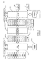
図4は、頂点シェーダと圧縮操作のための、グラフィック処理ユニット (GPU)34の一般的なブロック・ダイアグラムを示す。GPU34は、VS入力レジスタ・ファイル56に複数個の属性を出力する、ストリーム・デコーダ50を含む。これらの属性は、頂点シェーダ(VS)60により受け取られる。VS60の出力は、VS出力レジスタ・ファイル57に記憶されている、ヴァリングを含んでいる。認めていただけるように、「レジスタ」ファイルは、情報を記憶する記憶媒体のように、ハードウェア構成要素である。この場合に、「VS入力レジスタ・ファイル」は、VS60に送信されるべきである、入力ファイルを記憶する。単純にするために、大半の場合において、VS入力レジスタ・ファイル56を参照する時に、VS60への「入力ファイル」および/または「入力ファイル」を記憶するためのハードウェアが参照されている。同様に、単純にするために、大半の場合において、VS出力レジスタ・ファイル57を参照する時に、VS60からの「出力ファイル」および/または「出力ファイル」を記憶するためのハードウェアが参照されている。後に、さらに詳細に説明されるように、これらのヴァリングは、第1のレベルのヴァリング圧縮のために、コンパイラ62(図6)によってインテリジェントに圧縮される。VS出力レジスタ・ファイル57におけるヴァリングは、連続して、直列に、または、連鎖シーケンスとして、第2のレベルのヴァリング圧縮において、ヴァリングを圧縮する、圧縮バッファ58に送られる。圧縮バッファ58が満たされると、圧縮されたヴァリングは、次に、頂点キャッシュ54に記憶される。
FIG. 4 shows a general block diagram of a graphics processing unit (GPU) 34 for vertex shaders and compression operations. The
以下の説明から理解されるように、VS出力レジスタ・ファイル57とVS入力レジスタ・ファイル56は、それぞれ、複数個の共有M次元(MD)レジスタを含む。各々の圧縮バッファ58と52は、少なくとも1つの共有M次元(MD)レジスタを含む。
As will be understood from the following description, the VS
図4の構成において、ストリーム・デコーダ50は、バイパスされたストリームとバイパスされないストリームの、2つのストリームを発生する。バイパスされないストリームは、VS入力レジスタ・ファイル56に送られ、好ましくは、テーブル1に示される方法によって、また、圧縮される。バイパスされた属性は、圧縮バッファ52に圧縮される。バイパスされた属性は、図8A、8B,9A,9B、10A,10B、11A,11B,12Aと12Bに関して、後に詳細に説明される。
In the configuration of FIG. 4, the stream decoder 50 generates two streams, a bypassed stream and a non-bypassed stream. The non-bypassed stream is sent to the VS
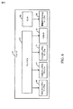
図5は、フラグメント・シェーダと関連付け操作を含む、グラフィック処理ユニット(GPU)の一般的なブロック・ダイアグラムを示す。圧縮されたヴァリングは、頂点キャッシュ54に記憶されている。プリィミティブ・アセンブラとラスタライザ90は、頂点キャッシュ54のヴァリングを、入力として受け取る。プリィミティブ・アセンブラとラスタライザ90は、圧縮されたヴァリングを、ヴァリングバッファ92に出力する。関連付けユニット88は、ヴァリング再マッピングおよびロード・モジュール84によって使用される、1組の関連付け命令82を持つ。図6のリンカ80は、ドライバ61により、図5の関連付け命令82のために、記憶装置にロードされる、関連付け(linking table)テーブル86を発生する。VS出力シンボル・テーブル(表2)に圧縮されたヴァリングを、FS入力シンボル・テーブル(表3)に関連付ける、関連付けテーブル86の例が、以下に説明される表4と表6に示される。FS入力シンボル・テーブルは、VS出力シンボル・テーブルよりも少ないシンボルを持つことができる。関連付け・ユニット88により、関連付け処理が実行された後に、ヴァリング再マッピングおよびロード・モジュール84からのヴァリングは、フラグメント・シェーダ(FS)70による使用のために、FS入力レジスタ・ファイル79に送られる。
FIG. 5 shows a general block diagram of a graphics processing unit (GPU), including fragment shaders and association operations. The compressed valing is stored in the
図6は、ドライバの一般的なブロック・ダイアグラムを示す。ドライバ61は、コンパイラ62とリンカ80を含んでいる。コンパイラ62は、VS入力シンボル・テーブル64とVS出力シンボル・テーブル66を発生する。例示のVS入力シンボル・テーブルが、以下に、表1に示される。例示のVS出力シンボル・テーブルが、以下に、表2に示される。コンパイラ62は、頂点シェーダ60とフラグメント・シェーダ70を独立にコンパイルすることができるので、コンパイラ62は、VS出力シンボル・テーブル66におけるIDごとに、FS入力シンボル・テーブル74におけるそれとは異なる、同じシンボルを割り当てることができる。このように、ドライバ61のためのリンカ80が、VS出力シンボル・テーブル66内のレジスタIDと、FS入力シンボル・テーブル74内のレジスタIDの間で、両方のテーブルで同じシンボルを見つけることによる、マッピングを実行するために存在する。リンカ80は、同じヴァリングシンボルを見つけるために、フラグメント・シェーダ70の入力レジスタ・ファイル79内の、対応する入力レジスタに、(頂点キャッシュ54またはヴァリングバッファ92の場所に対応する)ヴァリングをロードするために、GPU34と通信する。
FIG. 6 shows a general block diagram of the driver. The
ドライバ61は、1組の命令を持つ、ソフトウェア・ドライバである。コンパイラ62とリンカ80は、CPU32またはコントローラ/プロセッサ26上で動作するソフトウェア・ドライバ61の部分である。これに対して、GPU34は、ドライバ61によって命令される、特殊なコプロセッサである。
The
表1に示される、VS入力シンボル・テーブルは、以下の入力、すなわち、属性名、タイプ、もともと割り当てられた属性入力レジスタID、もともとのマスク、新たに割り当てられた属性入力レジスタID、および、新しいマスク、を含んでいる。表2に示される、VS出力シンボル・テーブルは、以下の入力、すなわち、ヴァリング名、タイプ、もともと割り当てられていたヴァリング出力レジスタID、もともとのマスク、新たに割り当てられたヴァリング出力レジスタID、および、新しいマスク、を含んでいる。テーブルにおけるマスクは、GPU34のハードウエア(HW)に割り当てられた、規定のMD(M=4)ベクトル・レジスタ記憶に対応する、属性ベクトル、または、ヴァリングベクトルのための、有効な成分を表す。もともと割り当てられていたIDとマスク、および、新たに割り当てられるIDとマスクは、両方とも、単に図示のために、以下の表内に一緒にされている。実際には、もともと割り当てられていたIDとマスクは、一時的な結果であり得るし、操作中に、同じ記憶場所を使用して、新たに割り当てられたIDとマスクになり得る。
The VS input symbol table shown in Table 1 includes the following inputs: attribute name, type, originally assigned attribute input register ID, original mask, newly assigned attribute input register ID, and new Mask. The VS output symbol table shown in Table 2 includes the following inputs: Varing name, type, originally assigned Valing output register ID, original mask, newly assigned Valing output register ID, and Includes a new mask. Mask in the table, assigned to the hardware (HW) of the
コンパイラ62は、gl_FragColor FC(図2)として示される、FS入力シンボル・テーブル74とFS出力シンボル・テーブル76を発生する。表3に示される、FS入力シンボル・テーブル74は、以下の入力、すなわち、ヴァリング名、タイプ、もともと割り当てられていたヴァリング入力レジスタID、もともとのマスク、新たに割り当てられたヴァリング入力レジスタID、および、新たなマスク、を含んでいる。
The
以下の表1と表2において、最後の2つの列は、以下に説明される圧縮処理に従って、新たに更新されている。

ヴァリング(varyings)は、実数型、二次元(2D)ベクトル、3次元(3D)ベクトル、4次元(4D)ベクトル、配列、および、2D/3D/4D行列等であり得る。OpenGL ESシェーディング言語の仕様は、モバイルGPU34でサポートされる、少なくとも32個のヴァリング成分を必要とする。各々のヴァリングは、異なる大きさを持ち、通常は、それ自身のレジスタ/バッファ空間を確保する。頂点キャッシュ54において、レジスタは、通常は、4Dベクトルである。さらに、VS入力レジスタ・ファイル56に対応するレジスタと、VS出力レジスタ・ファイル57に対応するレジスタは、通常は4Dベクトルである。ヴァリングの圧縮は、各々の頂点または画素のための連続空間に、異なるヴァリングをタイトに、一緒に入れる。例えば、ここに説明されたヴァリング圧縮は、2つの2Dベクトルを、1つの4次元ベクトル・レジスタに入れる。他の例では、ヴァリング圧縮は、1つの4Dベクトル・レジスタに、1つの3次元ベクトルと1つの実数(1D)を入れるであろう。それらをタイトに圧縮しないと、それらは、ゆったりと記憶され得る。
Varyings can be real, two-dimensional (2D) vectors, three-dimensional (3D) vectors, four-dimensional (4D) vectors, arrays, 2D / 3D / 4D matrices, and the like. The OpenGL ES shading language specification requires at least 32 Valing components supported by the
上記の説明は、ヴァリングに関連している。しかしながら、ヴァリングに加えて、属性も圧縮され得る。 The above description relates to Valing . However Na grounds, in addition to Varingu, attributes may also be compressed.
図7は、2レベルのシェーダ変数の圧縮処理100の、一般的なフローチャートを示す。処理100は、コンパイラ62に命令されて、インテリジェントな圧縮が行われるブロック102において、開始する。ブロック102では、成分の合計がMと等しい,2つ以上のシェーダ変数が、共有M次元(MD)ベクトル・レジスタに対して、割り当てられる。図示を可能にするために、VS出力レジスタ・ファイル57が列と行により示される。各々の行は、X,Y,ZとWで示される4個(4)のブロックを持つ。ブロック102の後に、ブロック104が続き、そこでは、VS出力レジスタ・ファイル57内のシェーダ変数を、頂点キャッシュ54のN×M記憶媒体ブロック内で、連続的に、直列に圧縮する、ハードウェアのヴァリング圧縮が、圧縮バッファ58において実行される。
FIG. 7 shows a general flowchart of a two-level shader
図7のシェーダ変数は、ヴァリングである。 The shader variable in FIG. 7 is Valing .
以下の説明からわかるように、バイパスされた属性は、図13Aに関して説明された、ブロック104の処理と同様に、圧縮バッファ52の中で圧縮される。バイパスされていない属性は、ブロック102に関して上に説明された処理を使用して圧縮され得る。このように、圧縮処理100は、属性のために使用され得る。したがって、シェーダ変数は、ヴァリングまたは属性を含む。
As can be seen from the following description, the bypassed attributes are compressed in the
第1のレベル:コンパイラ・レベル圧縮
コンパイラ62により命令される、ブロック102におけるインテリジェントな圧縮の、以下の説明は、表1と表2に関して説明されるであろう。インテリジェントな圧縮が、シェーダ変数(ヴァリングと属性の両方)に適用される。表1は、属性の圧縮を図示していて、表2は、ヴァリングの圧縮を図示している。コンパイラ62は、同一の、または、共通のMD(M次元)ベクトル・レジスタを再割り当てし、ここにおいて、レジスタIDを、その成分の和がM(M=4)と等しい、2つ以上のヴァリングに関連付けることにより、バイパスしない属性またはヴァリングの圧縮を実行し、これにしたがって、マスクを更新する。属性のためのMDベクトル・レジスタは、図4におけるVS入力レジスタ・ファイル57のための記憶に対応する。ヴァリングのためのMDベクトル・レジスタは、図4におけるVS出力レジスタ・ファイル57のための記憶に対応する。例示の設定M=4において、このように、ベクトルはX,Y,ZとWにより示される。それにもかかわらず、より多いまたはより少ない次元の他の設定が使用され得る。
First Level: Compiler Level Compression The following description of intelligent compression in
マスクはMビットの位置を持つ。このように、各々の再割り当てされた、および/または、結合された、特定のMDベクトル・レジスタのための、属性またはヴァリング(シェーダ変数)に関連付けられたマスクが、共通MDベクトル・レジスタのどの部分が、後の記憶と使用のために、各々の明確な属性または(組み合わせの)ヴァリングに割り当てられているかを示し、識別するために使用される。 The mask has a position of M bits. In this way, the mask associated with the attribute or varing (shader variable) for each reassigned and / or combined specific MD vector register is the one in the common MD vector register. Used to indicate and identify whether a portion is assigned to each distinct attribute or (combination) walling for later storage and use.
例えば、上記の表1の特定の参照において、texcoord0とtexcoord1は、もともとはID番号が「もともと割り当てられていた属性入力レジスタID」の列の中に、それぞれ、3と4により示される、異なる属性入力レジスタに割り当てられていた。さらに、texcoord0とtexcoord1のための、もともとのマスクは、それぞれ、0011と0011である。コンパイラ62は、texcoord0とtexcoord1の両方が、そのベクトルの合計が4D(M=4)ベクトルに等しい、2Dベクトルであることを決定する。したがって、コンパイラ62は、texcoord0とtexcoord1の、「新たに割り当てられた属性入力レジスタID」行内の、ID番号3で示される、同じ属性レジスタへの圧縮を命令する。圧縮中には、表1の「新しいマスク列」の中で、texcoord0は、マスクの最下位ビット位置0011に割り当て得るし、texcoord1は、マスクの最上位ビット位置1100に割り当て得る。マスク0011は、MDベクトル・レジスタ3のどの部分に、texcoord0に対応するデータを見つけ得るのかを示す。同様に、マスク1100は、MDベクトル・レジスタ3のどの部分に、texcoord1に対応するデータを見つけ得るのかを示す。この用語は、2つ以上の属性が、重なり合わない方法で、共通のレジスタを共有することを許容する。認識していただけるように、マスク内のビット数は、次元に依存して変化するであろう。
For example, in the specific reference in Table 1 above, texcoord0 and texcoord1 are different attributes, originally indicated by 3 and 4, respectively, in the column of attribute input register IDs originally assigned ID numbers. It was assigned to the input register. Further, the original masks for texcoord0 and texcoord1 are 0011 and 0011, respectively. The
表2により最も良くわかるように、VS出力シンボル・テーブル66のヴァリングtexcoord0とtexcoord1の特定の参照により、これらは、「新規に割り当てられたヴァリングレジスタ出力ID」の列の中に示される、ID番号0を持つ、同じヴァリングレジスタ内に圧縮される。texcoord0のための新しいマスクは、古いマスクと同じ、0011である。しかしながら、texcoord1のための新しいマスクは、古いマスクとは異なる、1100である。このように、マスクは、各々のビットが共有MDベクトル・レジスタ内での位置を表す、Mビットを持つ。 As best seen by Table 2, the specific reference to Varingu texcoord0 and texcoord1 of the VS output symbol table 66, it is shown in the column of "Varingu register output ID assigned to the new", ID number Compressed into the same Valing register with zero. The new mask for texcoord0 is 0011, the same as the old mask. However, the new mask for texcoord1 is 1100, which is different from the old mask. Thus, the mask has M bits, where each bit represents a position in the shared MD vector register.
もう1つの例において、VS入力シンボル・テーブル64の属性、「重み付け」と「標準」は、表1の「新たに割り当てられた属性入力レジスタID」と示される、ID番号2を持つ、同じ属性レジスタに圧縮される。コンパイラ62が、レジスタIDと「新しいマスク」の再割り当てを命じた後に、GPU34のハードウェア(HW)は、コンパイラ62により命令された第1のレベルの圧縮を終了する、(更新したマスクを含む)テーブルのような命令にしたがって、割り当てられたレジスタに、対応するシェーダ変数(属性とヴァリング)を、自動的にロードするであろう。
In another example, the attributes of the VS input symbol table 64, “weighting” and “standard” are the same attributes with ID number 2 shown in Table 1 as “Newly Assigned Attribute Input Register ID”. Compressed into registers. After the
配列または行列は、2D/3D/4Dベクトル、または、1つの実数型(float)に、論理的に分割され得るし、その時、コンパイラ62によって命令されるように、圧縮が実行され得る。配列は一連の実数型、2Dベクトル、3Dベクトル、または、4Dベクトルにより表すことができる。例えば、10個の実数型の配列は、1つの2Dベクトルを加えた、2個の4Dベクトルに、または、10個の独立実数型に分割することができる。2×2のマトリクスは、2つの2Dベクトルに、3×3のマトリクスは、3つの3Dベクトルに、4×4のマトリクスは、4つの4Dベクトルに、それぞれ分割し得る。したがって、コンパイラ62は、以下のような場合、2Dベクトル+2Dベクトル、3Dベクトル+実数型、2Dベクトル+実数型[+実数型]および、実数型+実数型[+実数型[+実数型]]には、圧縮を命じることができる。これらの例は、4Dベクトル・レジスタについてである。他の組み合わせは、次元の数に基づいて描かれる。入力レジスタ・ファイルと出力レジスタ・ファイルの使用は、第1のレベルの圧縮により最小化され得る。
The array or matrix can be logically divided into 2D / 3D / 4D vectors, or a single float, at which time compression can be performed as instructed by the
コンパイラ62に命令された圧縮の後に、全てのシェーダ変数(ヴァリング)は、まだ、4D(MD)ベクトルに配列されていないであろうし、例えば、いくつかの3Dベクトル、いくつかの4Dベクトル等が存在するであろう。例示の構成において、第2のレベルのヴァリング圧縮のために、ヴァリング記憶または頂点キャッシュ54内に、ヴァリングをタイトにHW圧縮するメカニズムが実行される。
After compression commanded to the
第2のレベル:HW圧縮
ヴァリングの記憶または頂点キャッシュ54において、1つの頂点または1つのピクセルのための、全てのヴァリングはN×Mのバッファ・ブロックに記憶される。Nはヴァリングの数であり、M=4は4Dベクトルであることを意味する。記憶装置ブロックは、連続的な(一連の)成分(component)の数(N×M)として取り扱われ得る。32ビット/成分とM=4の場合には、成分は0〜((Nx4)−1)で番号付けされ得る。例えば、N=8で8×4の記憶媒体ブロックは、0〜31で番号付けされる、32個の連続的な(一連の)成分として取り扱われ得る。
Second level: HW compression
In the Varing Store or
図4において、圧縮バッファ58は、2×M(M=4)のスロットの配列として表される。矢印は、圧縮バッファ58において、スロットを満たす方向を示す。圧縮バッファ58の上端の行は、一時バッファ58Aとして示され、2番目の行は、作業バッファ58Bとして示される。表5は、HW圧縮の結果を図示する。
第2のレベルの圧縮は、一時バッファ58A(圧縮バッファ58の第1行)を、連続的にかつ直列に、最初に満たすことによって、HWにおいて実行され得る。圧縮バッファ58の一時バッファ58Aが満たされると、一時バッファ58Aの内容は頂点キャッシュ54内での記憶のために転送され得る。この構成において、圧縮バッファ58は、一時バッファ58Aとして示される、Mスロットの第1の行と、作業バッファとして示されるMスロットの第2の行を含む。
A second level of compression may be performed at the HW by first filling the
表5で説明されている例を使用すると、HW圧縮は、VS出力レジスタ・ファイル57から、V0.x、V0.yとV0.zとして示される3つの成分を持つ、ヴァリングV0を読み出し、ヴァリングV0.x、V0.yとV0.zによりX,Y,ZとWの一時バッファ58A(最も上の行)のスロットを満たすことから始まる。理解され得るように、一時バッファ58AのスロットWは空である。一時バッファ58Aが満たされるまでは、ヴァリングV0.x、V0.yとV0.zは、まだ、頂点キャッシュ54に送られていない。
Using the example described in Table 5, HW compression is performed from the VS
HW圧縮は、VS出力レジスタ・ファイル57から、V1.x、V1.y、V1.z、V1.wと示される、4つの成分を持つヴァリングV1を読み出し、一時バッファ58Aにおける、残りのスロットを満たすことにより、継続する。この場合に、一時バッファ58A(上の行)のスロットWは、ヴァリングV1.xにより満たされている。残りのヴァリング成分V1.y、V1.z、V1.wは、第2の行または作業バッファ58BのスロットX,YとZ内に、連続的に満たされる。一時バッファ58Aが完全に満たされると、一時バッファ58Aを空にするために、一時バッファ58Aの内容は、頂点キャッシュ54の(第1の)行に書き込まれ得る。
HW compression is performed from the VS
一時バッファ58Aが空であると、作業バッファ58AのスロットX,YとZ内に、連続的に満たされている、残りのヴァリング成分V1.y、V1.z、V1.wの内容が、一時バッファ58Aに転送される。再び、一時バッファ58Aは満たされていない。このように、HW圧縮は、VS出力レジスタ・ファイル57から、V2.x、とV2.yにより示される、2つの成分を持つヴァリングV2を読み出し、一時バッファ58Aにおける、残りのスロットを満たすことにより、継続する。この場合には、一時バッファ58AのスロットW(上の行)は、ヴァリングV2.xにより満たされている。残りのヴァリング成分V2.yは、第2行のスロットX、または、作業バッファ58B内に満たされる。一時バッファ58Aが完全に満たされると、一時バッファ58Aを空にするために、一時バッファ58Aの内容は、頂点キャッシュ54の(第2の)行に書き込まれ得る。
If the
処理は、VS出力レジスタ・ファイル57におけるヴァリングのために、継続する。この例では、最後のヴァリングが、一時バッファ58AのX,YとZのスロットだけを満たすので、内容は、マスク=xyz、または、(111)としてヴァリング記憶、または、頂点キャッシュ54に書き込まれる。
Processing continues due to varing in the VS
圧縮バッファ58の、一時バッファ58Aと作業バッファ58Bは、性能のためにある。一時バッファ58Aが満たされていて、ヴァリング記憶、または、頂点キャッシュ54に書き出す準備ができている時に、他のバッファ(作業バッファ58B)が同時に満たされ得る。読み出しバスと書き込みバスの両方は、同時に、4個の(M個の)成分のために使用され得る。1回の読み出し、または、書き込みが4個未満の成分である場合には、読み出され、書き込まれる上で、どの成分が有効であるかを示すために、読み出しまたは書き込みマスクが使用される。
The
第2のレベルのHW圧縮が完了すると、VS出力シンボル・テーブル(表2)における圧縮されたヴァリングに対応する、表4の「新規に割り当てられたVSヴァリング出力レジスタID」に対応するレジスタIDは、表6における「新規に割り当てられたVSヴァリング出力レジスタID」の列に示される、出力ヴァリング記憶、または、頂点キャッシュ54に対応するように変更されるであろう。単純化と柔軟化のために、出力IDと頂点キャッシュ54内の位置の関係は、ベクトル・レジスタの代わりに成分ユニットに基づいて割り当てられる。この例では、ID=0であるtexcoord0と、ID=2であるtexcoord1が、ヴァリング記憶、または、頂点キャッシュ54の第1の行に、ID=4であるcolor0は第2の行に、ID=8であるcolor1Iは第3の行に、圧縮される。位置とtexcoord2は、FS70においては使用されないので、FS入力レジスタ・ファイル79においては、記憶/圧縮がこれらには割り当てられない。このように、「新規に割り当てられたFSヴァリング入力レジスタID」は、表4または表6では提供されない。
When the second level of HW compression is complete, the register ID corresponding to “Newly Assigned VS Varing Output Register ID” in Table 4 corresponding to the compressed Valing in the VS Output Symbol Table (Table 2) is , Will be modified to correspond to the output variable storage or
第2のレベルのHW圧縮は、HWによって実行されるが、表6に示されるように、関連付けテーブル86はドライバ61のリンカ80によって、更新される。ドライバ61は、図4における、同じ圧縮メカニズムに基づく各々のヴァリング成分、および、VS入力と出力シンボル・テーブル64と66、およびFS入力シンボル・テーブル74等のために、ヴァリング記憶または頂点キャッシュ54内の、新たなレジスタID/成分IDを計算することができる。表4は、関連付けテーブルが、第2のレベルのHW圧縮なしで、何を表そうとしているのかを図示する。表6は、関連付けテーブルが、HW圧縮の後で、何を表そうとしているのかを図示する。
VS60のような、プログラム可能な頂点シェーダは、PCゲーム・デバイスおよびモバイル・デバイスの両方において、最新のGPUの重要な計算ユニットである。VS60は、計算する上で電力を消費し、その上に、通常は、性能のボトルネックである。しかしながら、いくつかの応用は、シェーダ機能を使用しなくでもよい。別の考え方は、VS60への何らかの入力は、何の計算も必要としないで、直接出力に移動され得る。
Programmable vertex shaders, such as VS60, are an important computational unit for modern GPUs in both PC gaming and mobile devices. The
この機能についての、最も単純な解決策は、全ての入力を頂点シェーダ内に導き、ここにおいて、頂点シェーダが移動命令を実行することである。しかしながら、そのような解決策は、多くの計算の電力を消費し、頂点シェーダに、性能における低下を持たせるであろう。性能の低下は、1)データの入力/出力のための、不必要なトラフィック・バンド幅と、2)頂点シェーダにおいて実行される不必要な移動命令の結果である。 The simplest solution for this function is to direct all inputs into the vertex shader, where the vertex shader executes the move instruction. However, such a solution would consume a lot of computational power and cause the vertex shader to have a degradation in performance. The performance degradation is the result of 1) unnecessary traffic bandwidth for data input / output and 2) unnecessary movement instructions executed in the vertex shader.
このように、GPU34は、入力ストリーム・デコーダ50からの入力をバイパスする経路を使用して、構築され、配置される。入力をバイバスする経路は、頂点キャッシュ54に直接行くことができる。ドライバ61、または、コンパイラ62は、どの入力が、頂点キャッシュ54に、直接バイパスされ得るか、どの入力が、頂点シェーダ60にロードしなければならないかを、指定することができる。コンパイラ62は、バイパスする入力のためのシェーダ・プログラムから、全ての不必要な移動命令を取り除く。
In this manner, the
図4に一点鎖線として示される、小さなハードウェア制御ロジック51は、入力ストリーム・デコーダ50の中にある。このように、受け取った入力が、「バイパスする」と指定されている場合には、入力フォーマットの復号の後に、入力は、バイパスされた経路に沿って送られ、頂点キャッシュ54に記憶されるであろう。「バイパスする」と示されていない、受け取った入力だけが、VS入力レジスタ・ファイル56において、圧縮され、頂点シェーダ60に送られる。
A small hardware control logic 51, shown as a dashed line in FIG. 4, is in the input stream decoder 50. Thus, if the received input is designated as “bypass”, after decoding the input format, the input is sent along the bypassed path and stored in the
例示の実施例において、バイパスされた属性は、頂点キャッシュ54に記憶される前に、圧縮バッファ52において圧縮される。コンパイラ62は、圧縮バッファ58Aに関連して上に説明されたような方法で、マスク、および/または、レジスタIDを修正するであろう。キャッシュ・インデックスは、バイパスされる入力と共に、頂点キャッシュ54に渡される。頂点シェーダ 60からの出力は、同じ頂点については、同じID/インデックスを持つであろう。したがって、頂点キャッシュ54は、頂点シェーダの出力に、バイパスした入力を容易に同期させることができる。
In the illustrated embodiment, the bypassed attributes are compressed in
図8Aと8Bは、バイパスする属性を除く前と後の、頂点シェーダ・プログラムを示す。いくつかの頂点シェーダは、L3とL4で示される列上に、MOV命令を持つ。MOV命令は、属性に関連づけられた入力レジスタから、ヴァリングに関連付けられた出力レジスタへの移動をさせる。そのような属性は、頂点シェーダ60からバイパスさせ得る。例えば、図8Aにおいて、パラメータV0,V1,V2は入力属性であり、oPos,oFog,oT0とoD0は、出力ヴァリングである。この例において、L1およびL3列上の入力属性v1と、L2およびL4列上の入力属性v2は、頂点シェーダ 60での何らの計算も含まず、oT0とoD0に単に移動される。したがって、属性v1とv2は、頂点シェーダ60のプログラム(1組の命令)が実行される前に、ヴァリング記憶、または、頂点キャッシュ54に直接バイパスされる。属性v1とv2がバイパスされた後に、これらは、図8Bの列L1,L2,L3とL4の削除によって示されるように、頂点シェーダ 60の中には送られないであろう。さらに、出力ヴァリングoT0とoD0は、図8Bにおいて列L3とL4が無いことで示されるように、頂点シェーダ 60から出力されない。したがって、バイパスする機能は、トラフィックのバンド幅と頂点シェーダ の計算電力を節約する。
8A and 8B show the vertex shader program before and after removing the bypass attribute. Some vertex shaders have MOV instructions on the columns denoted L3 and L4. The MOV instruction causes a move from the input register associated with the attribute to the output register associated with Valing . Such attributes may be bypassed from the
属性をバイパスするために、第2のレベルのHW圧縮が、以下に説明されるように、調整される。バイパスされた属性は、圧縮バッファ52においてのみ、第2のレベルのHW圧縮を受ける。圧縮バッファ52は、ストリーム・デコーダ50から、バイパスされた属性を受け取る。ストリーム・デコーダ50は、頂点ストリーム(属性)を、メイン(外部)メモリ40から取得し、異なる属性フォーマットからIEEEフロート・フォーマットにフォーマット変換する、責任を負う。ドライバ61は、どの属性がバイパスされるか、どの属性が頂点シェーダのために、VS入力レジスタ・ファイル56に送られるかを、ストリーム・デコーダ50に通信するであろう。バイパスされる属性は、上記の一時バッファ58Aと作業バッファ58Bを使用して、上に説明されたのと同じ様に、圧縮されるであろう。バイパスされない属性は、頂点シェーダ 60のVS入力レジスタ・ファイル57に送られ、圧縮されるであろう。
To bypass the attribute, the second level of HW compression is adjusted as described below. The bypassed attribute undergoes a second level of HW compression only in the
バイパスした属性とVS出力レジスタ・ファイル57の両方からのヴァリングは、全体のヴァリングの足跡(footprint)として、ヴァリング記憶、または、頂点キャッシュ54の全てを満たすであろう。単純化するために、バイパスされた属性からのヴァリングは、圧縮され、ヴァリング記憶、または、頂点キャッシュ54の最初の数行に記憶され、圧縮バッファ58に圧縮されたVS出力は、その後、ヴァリング記憶、または、頂点キャッシュ54に記憶される。例えば、図8Aを再び参照すると、ヴァリング出力(バイパスされた属性)oD0(v2)は、圧縮バッファ52の一時バッファ52Aに圧縮され、ヴァリング記憶、または、頂点キャッシュ54の第1行に記憶される。ヴァリング出力(バイパスされた属性)oT0(v1)は、ヴァリング記憶、または、頂点キャッシュ54の、2番目の行の、2つの重要度の低い成分に、圧縮または記憶される。VS出力oPoとoFogは、圧縮されるか、または、その後に、2番目の行の、2つの最も重要な成分から始めて、記憶されるであろう。この場合に。oPos.xyは、一時バッファのzwスロットに圧縮され、その時、書き込みマスク=zwとして、ヴァリング記憶、または、頂点キャッシュ54の2番目の行に書き込まれる。このように、それは、同じ行ではあるが、異なる成分の位置において、oT0の後に、連続して圧縮される。oPos.zwとoFogは、xyz成分スロットの作業バッファ52Bの中で圧縮され、書き込みマスク=xyzで、ヴァリング記憶、または、頂点キャッシュの、3行目に書き込まれるであろう。関連付けテーブル(link table)86は、それに応じて、更新されるであろう。
Valing from both the bypassed attribute and the VS
図9Aと9Bは、バイパスする属性を取り除いた前と後の、別の頂点シェーダ・プログラムを示す。「矢印L5,L6,L7,L8とL9」により示された列上の、移動命令は、バイパスされ得る。例えば、「矢印L5」によって示された列上では、ヴァリング出力oT0(v1)は、バイパスされ得る。他のヴァリング出力oT1(v1)、oT2(v3)、oD0(v4)とoD1(v5)も、また、バイパスされ得る。図9Bにおいて、図9Aの「矢印L5,L6,L7,L8とL9」により示された列が取り除かれている。 FIGS. 9A and 9B show another vertex shader program before and after removing the bypass attribute. Move commands on the column indicated by “arrows L5, L6, L7, L8 and L9” may be bypassed. For example, on the column indicated by “arrow L5”, the Valing output oT0 (v1) may be bypassed. The other Valing outputs oT1 (v1), oT2 (v3), oD0 (v4) and oD1 (v5) can also be bypassed. In FIG. 9B, the columns indicated by “arrows L5, L6, L7, L8 and L9” in FIG. 9A have been removed.
図10Aと10Bは、バイパスする属性が取り除かれる前と後の、さらなる頂点シェーダ・プログラムを示す。「矢印L10とL11」で示される列上での移動命令は、バイパスされ得る。図10Bにおいて、図10Aにおいて「矢印L10とL11」で示された列は、取り除かれている。 Figures 10A and 10B show additional vertex shader programs before and after the bypassing attribute is removed. Move commands on the columns indicated by “arrows L10 and L11” may be bypassed. In FIG. 10B, the columns indicated by “arrows L10 and L11” in FIG. 10A have been removed.
図11Aと11Bは、バイパスする属性を取り除く前と後の、さらなる頂点シェーダ・プログラムを示す。「矢印L12,L13,L14,L15とL16」により示された列上の、移動命令は、バイパスされ得る。図11Bにおいて、図11Aの「矢印L12,L13,L14,L15とL16」により示された列が、取り除かれている。 FIGS. 11A and 11B show additional vertex shader programs before and after removing the bypassing attribute. Move commands on the column indicated by “arrows L12, L13, L14, L15 and L16” may be bypassed. In FIG. 11B, the columns indicated by “arrows L12, L13, L14, L15 and L16” in FIG. 11A have been removed.
図12Aと12Bは、バイパスする属性を取り除く前と後の、さらなる頂点シェーダ・プログラムを示す。「矢印L17とL18」で示される、列上での移動命令は、バイパスされ得る。図12Bにおいて、図12Aにおいて「矢印L17とL18」で示された列は、取り除かれている。図8A,8B,9A,9B,10A,10B,11A,11B、12Aと12Bに示された例は、説明の目的であり、計算を必要としない他の移動命令または属性は、「バイパス属性」として示され得る。 Figures 12A and 12B show additional vertex shader programs before and after removing the bypassing attribute. The move commands on the columns indicated by “arrows L17 and L18” may be bypassed. In FIG. 12B, the columns indicated by “arrows L17 and L18” in FIG. 12A have been removed. The examples shown in FIGS. 8A, 8B, 9A, 9B, 10A, 10B, 11A, 11B, 12A and 12B are for illustrative purposes, and other movement instructions or attributes that do not require computation are “bypass attributes”. Can be shown as
容易に理解できるように、属性処理をバイパスすることの利点は、
1)シェーダのコードの大きさと実行する命令の低減、
2)入力/出力のトラフィック・バンド幅の低減、
3)ALU(算術と論理ユニット)の遅延時間とテクスチャをロードする遅延時間を扱い、より多くの頂点を許容するための、レジスタ・ファイルの大きさの低減、
4)遅延を取り扱う、より少ない命令とより多くの頂点による、より良い性能、
5)より少ない実行される命令とより少ないトラフィックによる電力節約、
6)シェーダには一般的である、バイパス/停止、
7)CPU/DSP32とGPU34の間の負荷バランスのために、シェーダ・プログラムの一部をCPUまたはDSPに移動させることにより、性能を調整するドライバ61のためのオプション、および、
8)予期されない問題の下で働くドライバ61のためのオプション、を含む。
To make it easier to understand, the benefit of bypassing attribute processing is
1) Reduction of shader code size and instructions to be executed,
2) Reduce input / output traffic bandwidth,
3) ALU (arithmetic and logical unit) delay time and delay time to load textures, reduce register file size to allow more vertices,
4) Better performance with fewer instructions and more vertices to handle delays
5) Power savings with fewer instructions executed and less traffic,
6) Common to shaders, bypass / stop,
7) Options for
8) Includes options for
実際のゲームおよびベンチマークから、大半の頂点シェーダ(VS)は、出力に、直接、移動されているある程度の入力を持つと判定されてきている。表7は、異なるシェーダ・プログラムと、ここに説明された、バイパス機能に基づいて、節約された入力トラフィックと節約された出力トラフィックを図示する。表7は、さらに、節約された命令の割合を提供する。
図13A−13Cは、属性のバイパスと結合された、シェーダ変数の圧縮プロセス200の一般的なフローチャートを示す。シェーダ変数の圧縮プロセス200は、図4のブロック・ダイアグラムに関して説明されるであろう。シェーダ変数の圧縮プロセス200は、ストリーム・デコーダ50によるように、入力属性のフォーマットが復号される、ブロック201から開始される。ブロック202は、ブロック201に続き、ここにおいて、ストリーム・デコーダ50からの属性が「バイパスされた属性」であるかどうかについて、決定がなされる。決定が「YES」であると、有効な(バイパスされた)属性成分が、一時バッファ52Aに蓄積される、ブロック204がブロック202に続く。一時バッファ52Aが満たされているかどうかを決定する、ブロック206が、ブロック204に続く。例として、Mの限界(M=4)のバイパスされた属性の成分が、一時バッファ52Aに満たされ得る。一時バッファ52Aは、また、作業バッファ52Bを満たすことにより、満たされる。
13A-13C illustrate a general flowchart of a shader
しかしながら、ブロック206における決定が「NO」であれば、処理は、ブロック211にループする。ブロック211は、最後の入力属性に到達したかどうかを評価する、決定ブロックである。ブロック211の詳細は、後で説明される。
However, if the determination in
一時バッファ52Aが満たされている時に、ブロック208がブロック206に続き、ここでは、一時バッファ52Aに記憶、または、満たされた、バイパスされた属性成分が、頂点キャッシュに54に送られ、記憶される。以上に説明されたように、作業バッファ52B内の、バイパスされた属性は、その時、満たされるか再び記憶されるまで、一時バッファ52Aに転送される。後に説明されるブロック211が、ブロック208に続く。
When
再び、ブロック202に戻って、属性がバイパスされない属性である場合には、ブロック202での決定が「NO」であることを意味しているが、前もって定義された圧縮命令に従って、バイパスしない属性が、ブロック210において、VS入力レジスタ・ファイル56に圧縮されるであろう。ブロック211が、ブロック210に続き、ここでは、最後の入力属性に到達したかどうかの決定を下す、決定が「NO」であると、ブロック211はループし、更なる入力属性が復号される、ブロック201に戻る。その逆に、決定が「YES」である場合には、ブロック212が、ブロック211に続き、そこでは、一時バッファ52A内の、残りのバイパスされた属性が頂点キャッシュ54に送られる。
Returning to block 202 again, if the attribute is an attribute that is not bypassed, it means that the decision at
ブロック213がブロック212に続き、そこでは、何らかのバイパスしない属性が、利用可能であるかどうかの決定が下される。決定が「NO」であると、処理200は終了する。しかしながら、ブロック213における決定が「YES」であると、その時、図13Bのブロック214が、ブロック213に続く。ブロック214において、バイパスしない属性が、その時、VS60に送られる。バイパスされない属性成分が、VS60に送られると、VS60は、ブロック216において、頂点シェーディング操作を行う。VS60が終了した後に、ブロック218における第1のレベルのコンパイラ圧縮を完了するシェーダ命令の実行中に、有効である出力のヴァリング成分は、VS出力レジスタ・ファイル57に自動的に圧縮される。ブロック218における圧縮は、図7のブロック102に対応する。
図13Cのブロック222は、ブロック218に続く。表5に関して上に説明されるように、VS出力レジスタ・ファイル57からの出力ヴァリングは、一時バッファ58Aに蓄積される。一時バッファ58Aは、作業バッファ58Bと結合して、満たされる。ブロック224は、ブロック222に続き、一時バッファ52Aが満たされているかどうかを決定する。もし「NO」であれば、ブロック222に戻る。決定が「YES」であると、ブロック226がブロック224に続き、一時バッファ58Aの内容が頂点キャッシュ54に送られる、ブロック228がブロック226に続き、それが、VS出力レジスタ・ファイル57内におけるファイルの最終であるかどうかを決定する。決定が「いいえ」であると、処理はブロック222に戻る。決定が「YES」であると、ブロック230がブロック228に続き、一時バッファ58A内の残りのヴァリング成分が頂点キャッシュ54に送られる。
圧縮の後に、トラフィック/バンド幅は減少させられる。記憶装置は、大いに利用され、さらに性能が改善される。 After compression, the traffic / bandwidth is reduced. Storage devices are greatly utilized and performance is further improved.
代わりの圧縮メカニズムが使用され得る。例えば、VS出力レジスタ・ファイル57内のヴァリングは、第2のレベルのHW圧縮を用いて圧縮されない。その代わりとして、ファイル57は、頂点キャッシュに、そのままコピーされる。表5に関しては、表5の左側は、頂点キャッシュ54にコピーされる。これは、同じレイアウトと形状を維持する。ラスタライザの結果がヴァリングバッファ92に送られる、プリィミティブ・アセンブラとラスタライザ90の後に、同じ圧縮メカニズムが実行される。プリィミティブ・アセンブラとラスタライザ90は、計算を節約するために、表2のマスクに基づいて、無効である(mask=0)成分のための計算を飛ばすであろう。
Alternative compression mechanisms can be used. For example, valing in the VS
リンカと関連付け(Linker & Linking)
VS60からのヴァリングは、FS70に入力されるであろう。このように、VS60のためのヴァリングシンボルは、コンパイラ62により発生され、VS出力シンボル・テーブル66に出力される。FS70のそれぞれの入力は、そのヴァリングシンボルまたはヴァリング名称によって定義されるように、VS出力シンボル・テーブル66における、それぞれのヴァリングシンボル出力に、結び付けられる。このように、VS出力シンボル・テーブル66(表1)における、「ヴァリング名称」により示される、ヴァリングシンボルが、FS入力シンボル・テーブル74(表3)における、「FSヴァリング名称」により示される、1つのエントリと一致すると、VS60からの出力(ヴァリング)は、FS70の入力に結び付けられる。VS60における順序と圧縮は、通常の場合には、FS70とは異なるので、リンカ80は、どのVS出力が、どのFS入力に結び付けられるかを決定する。リンカ80は、図5における、ヴァリングの再マッピングとローディング・モジュール84のために、関連付け命令82、または、関連付けテーブル86を発生する、ドライバ61の一部である。
Linker & Linking
Valing from
同様な関連付けソリューションが、頂点ストリーム・デコーダ50と、VS入力シンボル・テーブル64で示される、VS入力の間の関連付けのために適用される。さらに、関連付けソリューションは、FS出力シンボル・テーブル76により示されるFS出力と、サンプルごとの操作ユニットの入力の、関連付けに適用される。リンカ80は、任意の2個の隣接したプログラム可能な処理ステージのために使用され得る。
A similar association solution is applied for the association between the vertex stream decoder 50 and the VS input as indicated by the VS input symbol table 64. Furthermore, the association solution applies to the association of the FS output indicated by the FS output symbol table 76 with the input of the operating unit for each sample. The
図14は、関連付け処理(linking process)300の一般的なフロー・ダイアグラムを示す。関連付け処理300は、ブロック302から始まるが、ブロック302において、リンカ80は、VS出力シンボル・テーブル66とFS入力シンボル・テーブル76の両方から、同じシンボルを探し、比較する。ブロック304において、一致するシンボルに関連付けられたヴァリングは、ヴァリングバッファ92から読み出される。ブロック206は、ヴァリングをFS入力レジスタ・ファイル79に送る。このようにして、関連付けは完了する。例示の、結果として生じる関連付けテーブルが、表6に示される。関連付け処理300は、FS70に必要とされる各々のヴァリングのために、繰り返される。
FIG. 14 shows a general flow diagram of a
コンパイラ62における圧縮のために、VS出力シンボル・テーブル66は、FS入力シンボル・テーブル76とは異なる。このように、好ましい関連付け命令は、それぞれのヴァリング成分を基にして、定義される。
Due to compression in the
理解されるように、2つのレベルの圧縮は、ヴァリング(varying)のタイトな圧縮を可能にし、容易にする。第1のレベルのコンパイラの圧縮は、入力と出力を減少させ、これは、レジスタ・ファイルの大きさを低減する。HW圧縮は、単純で効率的である。圧縮処理は、さらに、入力/出力のトラフィック・バンド幅を、低減する。圧縮処理100または200は、キャッシュ記憶を大いに利用し、より少ないトラフィックにより電力を節約する。
As will be appreciated, the two-level compression allows for tight compression of Varingu (Varying), to facilitate. The first level of compiler compression reduces input and output, which reduces the size of the register file. HW compression is simple and efficient. The compression process further reduces the input / output traffic bandwidth. The
図4と5に示されるGPUパイプラインは、任意の2つの隣接するプログラム可能な処理ステージのために、一般的な関連付けを使用する。これは、階層的な関連付け、すなわち、配列と行列からベクトルと実数型へのような、大きくて複雑なヴァリングの構造のためのマッピングを、可能にする。圧縮処理は、コンパイラ62に、最適化のために、自由に、レジスタの再度の順序付け、または、再割り当てをすることを許容する。処理は、ドライバ/リンカが、VS出力の一部を、それらがFSにおいて使用されていない場合には、一部の関連付け命令を修正することにより、容易に取り除くことを許容する。
The GPU pipeline shown in FIGS. 4 and 5 uses a general association for any two adjacent programmable processing stages. This allows hierarchical associations, ie mapping for large and complex varing structures, such as arrays and matrices to vectors and real types. The compression process allows the
1つ以上の例示の構成において、記述された機能は、ハードウェア、ソフトウェア、ファームウェアまたは、任意の組み合わせによって実現されるであろう。ソフトウェアとして実現されると、機能は、コンピュータ可読媒体上の1つ以上の命令またはコードとして記憶されるか、または、送信される。コンピュータ可読媒体は、コンピュータ記憶媒体と、コンピュータ・プログラムとデータを1つの場所から他への転送を容易にする、任意の媒体を含む通信媒体の両方を含む。記憶媒体は、コンピュータによりアクセスができる、任意の利用可能な媒体であり得る。例としてであり、限定するものではないが、このようなコンピュータ可読媒体には、命令またはデータの構造の形式で、要求されるプログラムコードを輸送し、または、記憶するために使用され得る、および、コンピュータによりアクセスされ得る、RAM,ROM,EEPROM,CD−ROM,または、他の光ディスク記憶、磁気ディスク記憶、または、他の磁気記憶デバイス、または、任意の他の媒体が含まれる。さらに、任意の接続は、コンピュータ可読媒体と、適切に名づけられている。例えば、同軸ケーブル、光ファイバーケーブル、ツイストペア、ディジタル加入者線(DSL)、または、赤外線、無線およびマイクロ波のような無線技術を使用して、ソフトウェアがウェブサイト、サーバー、または、他の遠隔の供給源から送信される場合、そこでは、同軸ケーブル、光ファイバーケーブル、ツイストペア、DSL、または、赤外線、無線およびマイクロ波のような無線技術は、媒体の定義に含まれている。DiskとDiscは、ここで使用されるように、コンパクトディスク(CD)、レーザーディスク(登録商標)、光ディスク、ディジタル・バーサタイル・ディスク(DVD)、フロッピー(登録商標)ディスクおよびブルーレイ・ディスクを含んでいる。Disksは、普通の場合には、磁気的にデータを再生するが、Discsは、データを、レーザーを使って光学的に再生する。上記の組み合わせも、コンピュータ可読媒体の範囲に含めるべきである。 In one or more exemplary configurations, the functions described may be implemented by hardware, software, firmware, or any combination. When implemented as software, the functions are stored on or transmitted over as one or more instructions or code on a computer-readable medium. Computer-readable media includes both computer storage media and communication media including any medium that facilitates transfer of a computer program and data from one place to another. A storage media may be any available media that can be accessed by a computer. By way of example and not limitation, such computer readable media can be used to transport or store required program code in the form of instructions or data structures, and RAM, ROM, EEPROM, CD-ROM, or other optical disk storage, magnetic disk storage, or other magnetic storage device, or any other medium that can be accessed by a computer. In addition, any connection is appropriately named a computer readable medium. For example, using a coaxial cable, fiber optic cable, twisted pair, digital subscriber line (DSL), or wireless technology such as infrared, wireless, and microwave, the software can be a website, server, or other remote feed When transmitted from a source, coaxial technology, fiber optic cable, twisted pair, DSL, or wireless technologies such as infrared, radio and microwave are included in the definition of the medium. Disk and Disc, as used herein, include compact discs (CD), laser discs, optical discs, digital versatile discs (DVD), floppy discs and Blu-ray discs. Yes. Disks normally reproduces data magnetically, while Disks optically reproduces data using a laser. Combinations of the above should also be included within the scope of computer-readable media.
開示された構成の上記の説明は、任意の当業者が開示を作成し、利用することを可能にするために提供される。これらの構成に対する種々の修正は、当業者にとっては、容易に明白であり、ここに定義された一般的な原理は、本開示の精神または範囲から外れずに、他の構成に適用されるであろう。このように、本開示は、ここに示された構成に制限されることを意図していないし、ここに開示された原理と新規の特徴に矛盾しない最も広い範囲に一致する。
以下の本件出願の当初の特許請求の範囲に記載された発明を付記する。
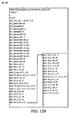
[C1]複数個の共有M次元(MD)レジスタを有する記憶媒体と、成分の合計がMに等しい1つ以上のシェーダ変数を各々の共有MDレジスタ内に圧縮する1組の操作を実行する処理ユニット、を含むデバイス。
[C2]前記1組の操作が、2つの2Dベクトル・シェーダ変数と、1つの3Dベクトル・シェーダ変数と1つの実数型シェーダ変数と、1つの2Dベクトル・シェーダ変数と2つの別の実数型シェーダ変数と、4つの実数型のシェーダ変数のうち1つを、圧縮する、C1のデバイス。
[C3]前記シェーダ変数が頂点シェーダからの1組の出力可変長を含み、前記1組の操作が、前記複数個の共有MDレジスタ内の、前記1組の出力可変長を圧縮する操作と、頂点シェーダ出力ファイルを生成するために、前記記憶媒体に任意の残りの可変長を充足する操作、を含む、C1のデバイス。
[C4]複数個のMDキャッシュ・レジスタを持つ頂点キャッシュをさらに含み、前記記憶媒体がMDレジスタを持つ圧縮バッファを含み、前記頂点シェーダ出力ファイルのM個の成分をその中に連続的に圧縮し、前記頂点キャッシュ内のそれぞれのMDキャッシュ・レジスタが満たされると、前記圧縮バッファの前記MDレジスタの内容を転送する、C3のデバイス。
[C5]前記処理ユニットが、前記頂点キャッシュ内の前記出力可変長を、フラグメント・シェーダの1組の入力可変長に関連付ける、第2の組の操作を実行する、C4のデバイス。
[C6]前記第2の組の操作が、前記頂点シェーダの前記出力可変長に対応する可変長シンボル名を、前記フラグメント・シェーダの前記組の入力可変長における対応する可変長シンボル名に一致させる操作を含む、C5のデバイス。
[C7]第2の複数個の共有MDレジスタを持つ、第2の記憶媒体をさらに含み、前記シェーダ変数が、さらに前記頂点シェーダの入力ためにバイパスされない入力属性とバイパスされる入力属性とを含み、前記1組の操作が、前記第2の複数個の共有MDレジスタ内の、前記バイパスされない入力属性を圧縮する操作と、頂点シェーダ入力ファイルを生成するために、前記第2の記憶媒体内に任意の残りのバイパスされない入力属性を充足する操作を含む、C4のデバイス。
[C8]前記頂点キャッシュが、第2の複数個のMDキャッシュ・レジスタをさらに含み、前記記憶媒体が、MDレジスタを持つ第2の圧縮バッファを含み、前記バイパスされる入力属性のM個の成分を、その中に連続的に圧縮し、前記頂点キャッシュ内の前記第2の複数個のMDキャッシュ・レジスタの各々のMDキャッシュ・レジスタが満たされると、前記第2の圧縮バッファの前記MDレジスタの内容を転送する、C7のデバイス。
[C9]第2の複数個の共有MDレジスタを持つ、第2の記憶媒体をさらに含み、前記シェーダ変数が前記頂点シェーダの入力ための1組の入力属性を含み、前記1組の操作が、圧縮された場合に、残りの圧縮されてない入力属性の成分がMを超えるまで、前記第2の複数個の共有MDレジスタ内の、前記1組の入力属性を圧縮する操作と、頂点シェーダ入力ファイルを生成するために前記第2の記憶媒体内に前記残りの入力属性を充足する操作を含む、C4のデバイス。
[C10]前記処理ユニットが、携帯電話、無線デバイス、無線通信デバイス、ビデオゲーム・コンソール、個人情報端末(PDA)、ラップトップ・コンピュータ、およびオーディオ/ビデオ対応デバイスの1つの一部である、C1のデバイス。
[C11]複数個の共有M次元(MD)レジスタを有する記憶媒体と、成分の合計がMに等しい1つ以上のシェーダ変数を各々の共有MDレジスタ内に圧縮する1組の操作を実行する処理ユニットを、含む集積回路。
[C12]前記1組の動作が、2つの2Dベクトル・シェーダ変数と、1つの3Dベクトル・シェーダ変数と1つの実数型のシェーダ変数と、1つの2Dベクトル・シェーダ変数と2つの別の実数型シェーダ変数と、4つの実数型のシェーダ変数のうち1つを、圧縮する、C11の集積回路。
[C13]前記シェーダ変数が頂点シェーダからの1組の出力可変長を含み、前記1組の操作が、前記複数個の共有MDレジスタ内の、前記1組の出力可変長を圧縮する操作と、頂点シェーダ出力ファイルを生成するために、前記記憶媒体に任意の残りの可変長を充足する操作、を含む、C11の集積回路。
[C14]複数個のMDキャッシュ・レジスタを持つ頂点キャッシュをさらに含み、前記記憶媒体が、MDレジスタを持つ圧縮バッファを含み、前記頂点シェーダ出力ファイルのM個の成分をその中に連続的に圧縮し、前記頂点キャッシュ内のそれぞれの(MD)キャッシュ・レジスタが満たされると、前記圧縮バッファの前記MDレジスタの内容を転送する、C13の集積回路。
[C15]前記処理ユニットが、前記頂点キャッシュ内の前記出力可変長を、フラグメント・シェーダのための1組の入力可変長に関連付ける、第2の組の操作を実行する、C14の集積回路。
[C16]前記第2の組の操作が、前記頂点シェーダの前記出力可変長に対応する可変長シンボル名を、前記フラグメント・シェーダのための前記組の入力可変長における対応する可変長シンボル名に一致させる操作を含む、C15の集積回路。
[C17]第2の複数個の共有MDレジスタを持つ、第2の記憶媒体をさらに含み、前記シェーダ変数が、さらに前記頂点シェーダの入力ためにバイパスされない入力属性とバイパスされる入力属性とを含み、前記1組の操作が、前記第2の複数個の共有MDレジスタ内の、前記バイパスされない入力属性を圧縮する操作と、頂点シェーダ入力ファイルを生成するために、前記第2の記憶媒体内に任意の残りのバイパスされない入力属性を充足する操作を含む、C14の集積回路。
[C18]前記頂点キャッシュが、第2の複数個のMDキャッシュ・レジスタをさらに含み、前記記憶媒体が、前記バイパスされた入力属性のM個の成分をその中に連続的に圧縮し、前記頂点キャッシュ内の前記第2の複数個のMDキャッシュ・レジスタの各々のMDキャッシュ・レジスタが満たされると、前記第2の圧縮バッファの前記MDレジスタの内容を転送する、MDレジスタを持つ第2の圧縮バッファを含む、C17の集積回路。
[C19]第2の複数個の共有MDレジスタを持つ、第2の記憶媒体をさらに含み、前記シェーダ変数が前記頂点シェーダの入力ための1組の入力属性を含み、前記1組の操作が、圧縮された場合に残りの圧縮されてない入力属性の成分がMを超えるまで、前記第2の複数個の共有MDレジスタ内の、前記1組の入力属性を圧縮する操作と、頂点シェーダ入力ファイルを生成するために前記第2の記憶媒体内に前記残りの入力属性を充足する操作を含む、C14の集積回路。
[C20]前記処理ユニットが、携帯電話、無線デバイス、無線通信デバイス、ビデオゲーム・コンソール、個人情報端末(PDA)、ラップトップ・コンピュータ、およびオーディオ/ビデオ対応デバイスの1つの一部である、C11の集積回路。
[C21]1組のシェーダ変数を記憶するために複数個の共有M次元(MD)レジスタを含む記憶する手段と、成分の合計がMに等しい前記1組のシェーダ変数の1つ以上のシェーダ変数を各々の共有MDレジスタ内に圧縮する圧縮手段を、含むデバイス。
[C22]前記圧縮手段が、2つの2Dベクトル・シェーダ変数と、1つの3Dベクトル・シェーダ変数と1つの実数型のシェーダ変数と、1つの2Dベクトル・シェーダ変数と2つの別の実数型シェーダ変数と、4つの実数型のシェーダ変数の少なくとも1つを、圧縮するための手段を含む、C21の無線デバイス。
[C23]前記1組のシェーダ変数が頂点シェーダからの1組の出力可変長を含み、前記圧縮手段が、前記複数個の共有MDレジスタ内の前記1組の出力可変長を圧縮するための可変長圧縮手段と頂点シェーダ出力ファイルを生成するために前記記憶手段に任意の残りの可変長を充足する充足手段を含む、C21の無線デバイス。
[C24]前記1組のシェーダ変数が、頂点シェーダへの1組の入力属性を含み、前記圧縮手段が、前記複数個の共有MDレジスタ内の前記1組の入力属性を圧縮するための属性圧縮手段と、頂点シェーダ入力ファイルを生成するために前記記憶手段内に任意の残りの入力属性を充足するための充足手段を含む、C21の無線デバイス。
[C25]前記圧縮ユニットが、携帯電話、無線デバイス、無線通信デバイス、ビデオゲーム・コンソール、個人情報端末(PDA)、ラップトップ・コンピュータ、およびオーディオ/ビデオ対応デバイスの1つの一部である、C21の無線デバイス。
[C26]コンピュータに、そのベクトルの合計がMに等しい1組のシェーダ変数内の1つ以上のシェーダ変数を、複数個の共有MDベクトル・レジスタにおける各々の共有M次元(MD)ベクトル・レジスタに、圧縮させる命令を有するコンピュータ可読媒体を含むコンピュータ・プログラム製品。
[C27]前記シェーダ変数の組が頂点シェーダからの1組の出力可変長を含み、前記命令が、前記コンピュータに前記1組の出力可変長を圧縮させ、残りの出力可変長により、残りのベクトル・レジスタを充足させる、C26のコンピュータ・プログラム製品。
[C28]前記コンピュータに、前記圧縮された組の出力可変長を、フラグメント・シェーダのための1組の入力可変長に関連付けさせる命令を、さらに含む、C27のコンピュータ・プログラム製品。
[C29]前記関連付けさせる命令が、前記コンピュータに、前記頂点シェーダからの前記圧縮された組の出力可変長に対応する可変長シンボル名を、前記フラグメント・シェーダのための前記組の入力可変長における対応する可変長シンボル名に一致させる命令を含む、C28のコンピュータ・プログラム製品。
[C30]前記1組のシェーダ変数が、頂点シェーダへの1組の入力属性を含み、前記命令が、前記コンピュータに前記1組の入力属性を圧縮させ、残りの入力属性で残りのベクトル・レジスタを充足させる、C26のコンピュータ・プログラム製品。
[C31]そのベクトルの合計がMに等しい1組のシェーダ変数の内の1つ以上のシェーダ変数を、複数個の共有MDベクトル・レジスタにおける各々の共有M次元(MD)ベクトル・レジスタへ圧縮することと、任意の残っているシェーダ変数が圧縮できなくなるまで、前記複数個の共有MDベクトル・レジスタにおける前記圧縮を繰り返すこと、を含む方法。
[C32]前記1組のシェーダ変数が頂点シェーダからの1組の出力可変長を含み、前記圧縮が、前記複数個の共有M次元(MD)レジスタにおける、前記1組の出力可変長の圧縮を含む、C31の無線デバイス。
[C33]前記圧縮された出力可変長の組と残りの出力可変長により頂点シェーダ出力ファイルを生成することと、前記頂点シェーダ出力ファイルのM個の成分を、圧縮バッファのMD一時レジスタに連続的に圧縮することと、頂点キャッシュのそれぞれのMDキャッシュ・レジスタが満たされるとき、前記MD一時レジスタの内容の転送すること、をさらに含む、C31の方法。
[C34]前記組のシェーダ変数が頂点シェーダへのバイパスされない1組の入力属性を含み、前記圧縮が前記複数個の共有MDレジスタにおける前記組の入力属性の圧縮を含む、C31の方法。
[C35]バイパスされた入力属性のM個の成分を、圧縮バッファのMD一時レジスタに連続的に圧縮することと、頂点キャッシュのそれぞれのMDキャッシュ・レジスタが満たされるとき、前記MD一時レジスタの内容を転送すること、をさらに含む、C34の方法。
[C36]複数個の共有M次元(MD)レジスタを有する記憶媒体と、成分の合計がMに等しい1つ以上のシェーダ変数を各々の共有MDレジスタ内に圧縮する1組の操作を実装する集積回路を、含むプロセッサ。
[C37]前記シェーダ変数が頂点シェーダからの1組の出力可変長を含み、前記1組の操作が、前記複数個の共有M次元(MD)レジスタにおいて、前記1組の出力可変長を圧縮する操作と、頂点シェーダ出力ファイルを生成するために、前記記憶媒体に任意の残りの可変長を充足する操作を含むC36のプロセッサ。
[C38]複数個のMDキャッシュ・レジスタを持つ頂点キャッシュをさらに含み、前記記憶媒体がMDレジスタを持つ圧縮バッファを含み、前記頂点シェーダ出力ファイルのM個の成分をその中に連続的に圧縮し、前記頂点キャッシュ内のそれぞれのMDキャッシュ・レジスタが満たされると、前記圧縮バッファの前記MDレジスタの内容を転送する、C37のプロセッサ。
The above description of the disclosed configurations is provided to enable any person skilled in the art to make and use the disclosure. Various modifications to these configurations will be readily apparent to those skilled in the art, and the generic principles defined herein may be applied to other configurations without departing from the spirit or scope of the disclosure. I will. Thus, this disclosure is not intended to be limited to the configurations shown herein, but is consistent with the widest scope consistent with the principles and novel features disclosed herein.
The invention described in the scope of the claims of the present application below will be appended.
[C1] Processing to execute a set of operations to compress a storage medium having a plurality of shared M-dimensional (MD) registers and one or more shader variables whose sum of components is equal to M into each shared MD register Unit, including device.
[C2] The one set of operations includes two 2D vector shader variables, one 3D vector shader variable, one real type shader variable, one 2D vector shader variable, and two other real type shaders. A C1 device that compresses the variable and one of the four real shader variables.
[C3] the shader variable includes a set of output variable lengths from the vertex shader, and the set of operations compresses the set of output variable lengths in the plurality of shared MD registers; The device of C1, comprising an operation of satisfying any remaining variable length in the storage medium to generate a vertex shader output file.
[C4] further including a vertex cache having a plurality of MD cache registers, the storage medium including a compression buffer having MD registers, and continuously compressing the M components of the vertex shader output file therein A C3 device that transfers the contents of the MD register of the compression buffer when each MD cache register in the vertex cache is filled.
[C5] The device of C4, wherein the processing unit performs a second set of operations that associates the output variable length in the vertex cache with a set of input variable lengths of a fragment shader.
[C6] The second set of operations causes the variable length symbol name corresponding to the output variable length of the vertex shader to match the corresponding variable length symbol name in the input variable length of the set of fragment shaders. C5 device, including operations.
[C7] further including a second storage medium having a second plurality of shared MD registers, wherein the shader variable further includes an input attribute that is not bypassed and an input attribute that is bypassed for input of the vertex shader The set of operations in the second storage medium to generate a vertex shader input file and an operation to compress the non-bypassed input attributes in the second plurality of shared MD registers. The C4 device, including operations that satisfy any remaining non-bypassed input attributes.
[C8] The vertex cache further includes a second plurality of MD cache registers, the storage medium includes a second compression buffer having an MD register, and M components of the bypassed input attribute Are continuously compressed therein, and each MD cache register of the second plurality of MD cache registers in the vertex cache is filled, the MD register of the second compression buffer. A C7 device that transfers content.
[C9] further including a second storage medium having a second plurality of shared MD registers, wherein the shader variable includes a set of input attributes for input of the vertex shader, and the set of operations includes: An operation to compress the set of input attributes in the second plurality of shared MD registers until the remaining uncompressed input attribute components exceed M when compressed, and vertex shader input The C4 device, comprising an operation of satisfying the remaining input attributes in the second storage medium to generate a file.
[C10] The processing unit is part of one of a mobile phone, a wireless device, a wireless communication device, a video game console, a personal information terminal (PDA), a laptop computer, and an audio / video capable device Devices.
[C11] Processing to execute a set of operations to compress a storage medium having a plurality of shared M-dimensional (MD) registers and one or more shader variables whose sum of components is equal to M into each shared MD register An integrated circuit including a unit.
[C12] The one set of operations includes two 2D vector shader variables, one 3D vector shader variable, one real type shader variable, one 2D vector shader variable, and two other real types. A C11 integrated circuit that compresses a shader variable and one of four real-type shader variables.
[C13] The shader variable includes a set of output variable lengths from the vertex shader, and the set of operations compresses the set of output variable lengths in the plurality of shared MD registers; An integrated circuit of C11, comprising an operation of satisfying any remaining variable length in the storage medium to generate a vertex shader output file.
[C14] further including a vertex cache having a plurality of MD cache registers, the storage medium including a compression buffer having MD registers, and continuously compressing the M components of the vertex shader output file therein And an integrated circuit of C13 that transfers the contents of the MD register of the compression buffer when each (MD) cache register in the vertex cache is filled.
[C15] The integrated circuit of C14, wherein the processing unit performs a second set of operations that associates the output variable length in the vertex cache with a set of input variable lengths for a fragment shader.
[C16] The second set of operations changes the variable length symbol name corresponding to the output variable length of the vertex shader to the corresponding variable length symbol name in the input variable length of the set for the fragment shader. A C15 integrated circuit including a matching operation.
[C17] further including a second storage medium having a second plurality of shared MD registers, wherein the shader variable further includes an input attribute that is not bypassed and an input attribute that is bypassed for input of the vertex shader The set of operations in the second storage medium to generate a vertex shader input file and an operation to compress the non-bypassed input attributes in the second plurality of shared MD registers. The integrated circuit of C14, including operations that satisfy any remaining non-bypassed input attributes.
[C18] the vertex cache further includes a second plurality of MD cache registers, and the storage medium continuously compresses the M components of the bypassed input attribute into the vertex cache; A second compression having an MD register that transfers the contents of the MD register of the second compression buffer when each MD cache register of the second plurality of MD cache registers in the cache is filled; C17 integrated circuit including a buffer.
[C19] further including a second storage medium having a second plurality of shared MD registers, wherein the shader variable includes a set of input attributes for input of the vertex shader, and the set of operations includes: An operation to compress the set of input attributes in the second plurality of shared MD registers until the remaining uncompressed input attribute components exceed M when compressed, and a vertex shader input file; An integrated circuit of C14 including an operation of satisfying the remaining input attributes in the second storage medium to generate
[C20] The processing unit is part of one of a mobile phone, wireless device, wireless communication device, video game console, personal information terminal (PDA), laptop computer, and audio / video capable device, C11 Integrated circuit.
[C21] means for storing a plurality of shared M-dimensional (MD) registers for storing a set of shader variables, and one or more shader variables of the set of shader variables whose sum of components is equal to M Including compression means for compressing each into a shared MD register.
[C22] The compression means includes two 2D vector shader variables, one 3D vector shader variable, one real type shader variable, one 2D vector shader variable, and two other real type shader variables. And a C21 wireless device comprising means for compressing at least one of the four real shader variables.
[C23] The set of shader variables includes a set of output variable lengths from the vertex shader, and the compression means is a variable for compressing the set of output variable lengths in the plurality of shared MD registers. A wireless device of C21, comprising a length compression means and a fulfillment means for satisfying any remaining variable length in the storage means to generate a vertex shader output file.
[C24] The set of shader variables includes a set of input attributes to the vertex shader, and the compression means compresses the set of input attributes in the plurality of shared MD registers. A C21 wireless device comprising: means; and fulfillment means for satisfying any remaining input attributes in the storage means to generate a vertex shader input file.
[C25] The compression unit is part of one of a mobile phone, wireless device, wireless communication device, video game console, personal information terminal (PDA), laptop computer, and audio / video enabled device, C21 Wireless devices.
[C26] Causes the computer to transfer one or more shader variables in a set of shader variables whose vector sum is equal to M to each shared M-dimensional (MD) vector register in the plurality of shared MD vector registers. A computer program product comprising a computer readable medium having instructions to be compressed.
[C27] The set of shader variables includes a set of output variable lengths from a vertex shader, and the instruction causes the computer to compress the set of output variable lengths, and the remaining output variable lengths result in a remaining vector. A C26 computer program product that satisfies the register.
[C28] The computer program product of C27, further comprising instructions that cause the computer to associate the compressed set of output variable lengths with a set of input variable lengths for a fragment shader.
[C29] The instruction to associate causes the computer to obtain a variable length symbol name corresponding to the compressed set of output variable lengths from the vertex shader in the set of input variable lengths for the fragment shader. A C28 computer program product comprising instructions for matching a corresponding variable length symbol name.
[C30] The set of shader variables includes a set of input attributes to the vertex shader, and the instructions cause the computer to compress the set of input attributes and the remaining vector registers with the remaining input attributes A computer program product of C26 that satisfies
[C31] Compress one or more shader variables of a set of shader variables whose sum of vectors equals M to each shared M-dimensional (MD) vector register in a plurality of shared MD vector registers. And repeating the compression in the plurality of shared MD vector registers until any remaining shader variables cannot be compressed.
[C32] The set of shader variables includes a set of output variable lengths from the vertex shader, and the compression is a compression of the set of output variable lengths in the plurality of shared M-dimensional (MD) registers. Including C31 wireless devices.
[C33] generating a vertex shader output file with the set of compressed output variable lengths and the remaining output variable lengths, and successively adding M components of the vertex shader output file to the MD temporary register of the compression buffer And the method of C31 further comprising: compressing the content of the MD temporary register as each MD cache register of the vertex cache is filled.
[C34] The method of C31, wherein the set of shader variables includes a set of input attributes that are not bypassed to the vertex shader, and wherein the compression includes compression of the set of input attributes in the plurality of shared MD registers.
[C35] Continuously compressing the M components of the bypassed input attribute into the MD temporary register of the compression buffer, and when each MD cache register of the vertex cache is filled, the contents of the MD temporary register The method of C34, further comprising: transferring.
[C36] a storage medium having a plurality of shared M-dimensional (MD) registers and an integration that implements a set of operations that compress one or more shader variables whose sum of components equals M into each shared MD register A processor including a circuit.
[C37] The shader variable includes a set of output variable lengths from the vertex shader, and the set of operations compresses the set of output variable lengths in the plurality of shared M-dimensional (MD) registers. A C36 processor comprising an operation and an operation to fill any remaining variable length in the storage medium to generate a vertex shader output file.
[C38] further including a vertex cache having a plurality of MD cache registers, the storage medium including a compression buffer having MD registers, and continuously compressing the M components of the vertex shader output file therein The processor of C37, which transfers the contents of the MD register of the compression buffer as each MD cache register in the vertex cache is filled.
Claims (37)
少なくとも1つの共有M次元(MD)レジスタを有する記憶媒体であって、前記少なくとも1つの共有MDレジスタは、少なくとも1つの行を有し、各行は、少なくともMスロットを有する、記憶媒体と、
成分の合計がMに等しい、頂点シェーダ出力ファイルからの1つ以上のシェーダ変数を、前記少なくとも1つの共有MDレジスタの第1の行に連続的に圧縮し、
前記第1の行に前記1つ以上のシェーダ変数の各々をロードした後に、前記第1の行のMスロットが満たされているかどうかを検出し、
前記第1の行の前記Mスロットが満たされていないと検出した際に、前記第1の行を連続的に圧縮することを継続し、
前記第1の行の前記Mスロットが満たされていると検出した際に、前記少なくとも1つの共有MDレジスタの前記第1の行に圧縮された前記1つ以上のシェーダ変数を、頂点キャッシュ内のそれぞれのMDキャッシュ・レジスタに転送する、
ための1組の操作を実行する処理ユニットと、
を含む、デバイス。 A device,
A storage medium having at least one shared M-dimensional (MD) registers, said at least one shared MD register has at least one row, each row has at least M slots, and storage medium,
Continuously compressing one or more shader variables from a vertex shader output file with a sum of components equal to M into the first row of the at least one shared MD register ;
After loading each of the one or more shader variables into the first row, detecting whether the M slots of the first row are filled;
Continuing to compress the first row upon detecting that the M slots of the first row are not filled,
Upon detecting said first of said M slot line is satisfied, said at least one shared MD register of the first row the one or more shader variables compressed, vertex cache transfers of the each of the MD cache register,
A processing unit for performing a set of operations for
Including the device.
前記1組の操作が、
2つの2Dベクトル・シェーダ変数、
1つの3Dベクトル・シェーダ変数と1つの実数型シェーダ変数、
1つの2Dベクトル・シェーダ変数と2つの別の実数型シェーダ変数、および
4つの実数型のシェーダ変数、
のうち1つを、前記少なくとも1つの共有MDレジスタに圧縮する、請求項1のデバイス。 M is equal to 4,
The set of operations is
Variable two 2D vector shader,
One of the 3D vector shader variable and variable one of the real type shader,
One 2D vector shader variable and variable two separate real shaders, and four real shader variables,
The device of claim 1 , wherein one is compressed into the at least one shared MD register .
前記1組の操作が、前記少なくとも1つの共有MDレジスタにおいて前記1組の出力ヴァリング(varying)を圧縮する操作を含む、
請求項1のデバイス。The one or more shader variables include a set of output varyings from the vertex shader;
The set of operations, including operations for compressing said at least one said set in a shared MD register output Varingu (Varying),
The device of claim 1.
前記複数個のMDキャッシュ・レジスタは、前記それぞれのMDキャッシュ・レジスタを含み、
前記記憶媒体が前記少なくとも1つの共有MDレジスタを持つ圧縮バッファを含む、
請求項3のデバイス。A vertex cache having a plurality of MD cache registers;
The plurality of MD cash registers include the respective MD cash registers;
Including a compression buffer in which the storage medium has said at least one shared MD register,
請 Motomeko 3 of the device.
前記1つ以上のシェーダ変数が、さらに前記頂点シェーダの入力ためにバイパスされない入力属性とバイパスされる入力属性とを含み、
前記1組の操作が、前記複数個の共有MDレジスタの各々においてM個の前記バイパスされない入力属性を圧縮する操作と、頂点シェーダ入力ファイルにおいて任意の残りのバイパスされない入力属性を充足する操作とを含む、
請求項4のデバイス。With double several shared MD registers, further comprising a second storage medium,
The one or more shader variables further include an input attribute that is not bypassed and an input attribute that is bypassed for input of the vertex shader;
The operation set of operations, to fulfill operations and for compressing the input attributes in each of the previous Kifuku several shared MD registers not the M of the bypass, the input attributes are not any remaining bypass the vertex shader input file including the door,
The device of claim 4 .
前記記憶媒体が、MDレジスタを持つ第2の圧縮バッファであって、前記バイパスされる入力属性のM個の成分を、その中に連続的に圧縮し、かつ、満たされると、前記頂点キャッシュ内の前記第2の複数個のMDキャッシュ・レジスタの各々のMDキャッシュ・レジスタに、前記第2の圧縮バッファの前記MDレジスタの内容を転送するための、MDレジスタを持つ第2の圧縮バッファを含む、
請求項7のデバイス。The vertex cache further includes a second plurality of MD cache registers;
Said storage medium, and a second compression buffer with MD register, the M component of the input attribute to be the bypass, continuously compressed therein, and, when filled, the vertex cache to the second plurality of MD each MD cache register of the cash register, for transferring the contents of the MD register of the second compression buffer includes a second compression buffer with MD register ,
The device of claim 7 .
前記1つ以上のシェーダ変数が前記頂点シェーダの入力ための1組の入力属性を含み、
前記1組の操作が、圧縮された場合に、残りの圧縮されてない入力属性の成分がMを超えるまで、前記複数個の共有MDレジスタにおいて前記1組の入力属性を圧縮する操作と、頂点シェーダ入力ファイルにおいて前記残りの入力属性を充足する操作とを含む、
請求項4のデバイス。With double several shared MD registers, further comprising a second storage medium,
The one or more shader variables include a set of input attributes for the input of the vertex shader;
Operations and wherein the set of operations, when it is compressed, component of the input attributes not remaining compressed until greater than M, to compress the set of input attributes in the previous Kifuku several shared MD register in vertex shader input file containing operations that satisfy the remaining input attributes,
The device of claim 4 .
少なくとも1つの共有M次元(MD)レジスタを有する記憶媒体であって、前記少なくとも1つの共有MDレジスタは、少なくとも1つの行を有し、各行は、少なくともMスロットを有する、記憶媒体と、
成分の合計がMに等しい1つ以上のシェーダ変数を、前記少なくとも1つの共有MDレジスタの第1の行に連続的に圧縮し、
前記第1の行に前記1つ以上のシェーダ変数の各々をロードした後に、前記第1の行のMスロットが満たされているかどうかを検出し、
前記第1の行の前記Mスロットが満たされていないと検出した際に、前記第1の行を連続的に圧縮することを継続し、
前記第1の行の前記Mスロットが満たされていると検出した際に、前記少なくとも1つの共有MDレジスタの前記第1の行に圧縮された前記1つ以上のシェーダ変数を、頂点キャッシュ内のそれぞれのMDキャッシュ・レジスタに転送する、
ための1組の操作を実行する処理ユニットと、
を含む集積回路。 An integrated circuit,
A storage medium having at least one shared M-dimensional (MD) registers, said at least one shared MD register has at least one row, each row has at least M slots, and storage medium,
Continuously compressing one or more shader variables with a sum of components equal to M into the first row of the at least one shared MD register ;
After loading each of the one or more shader variables into the first row, detecting whether the M slots of the first row are filled;
Continuing to compress the first row upon detecting that the M slots of the first row are not filled,
Upon detecting that the M slot of the first row is full, the one or more shader variables compressed into the first row of the at least one shared MD register are stored in a vertex cache. Transfer to each MD cash register,
A processing unit for performing a set of operations for
Integrated circuit including a.
前記1組の操作が、
2つの2Dベクトル・シェーダ変数、
1つの3Dベクトル・シェーダ変数と1つの実数型シェーダ変数、
1つの2Dベクトル・シェーダ変数と2つの別の実数型シェーダ変数、および
4つの実数型のシェーダ変数、
のうち1つを、前記少なくとも1つの共有MDレジスタに圧縮する、請求項11の集積回路。 M is equal to 4,
The set of operations is
Variable two 2D vector shader,
One of the 3D vector shader variable and variable one of the real type shader,
One 2D vector shader variable and variable two separate real shaders, and four real shader variables,
The integrated circuit of claim 11, wherein one is compressed into the at least one shared MD register .
前記1組の操作が、前記少なくとも1つの共有MDレジスタにおいて前記1組の出力ヴァリング(varying)を圧縮する操作を含む、
請求項11の集積回路。The one or more shader variables include a set of output varyings from the vertex shader;
The set of operations, including operations for compressing said at least one said set in a shared MD register output Varingu (Varying),
The integrated circuit of claim 11.
前記複数個のMDキャッシュ・レジスタは、前記それぞれのMDキャッシュ・レジスタを含み、
前記記憶媒体が前記少なくとも1つの共有MDレジスタを持つ圧縮バッファを含み、前記圧縮バッファは、前記頂点シェーダ出力ファイルのM個の成分を、前記頂点キャッシュ内の前記それぞれのMDキャッシュ・レジスタに連続的に圧縮するように構成される、
請求項13の集積回路。A vertex cache having a plurality of MD cache registers;
The plurality of MD cash registers include the respective MD cash registers;
The storage medium includes a compression buffer having the at least one shared MD register, the compression buffer sequentially transferring M components of the vertex shader output file to the respective MD cache registers in the vertex cache. Configured to compress,
The integrated circuit of claim 13.
前記1つ以上のシェーダ変数が、さらに前記頂点シェーダの入力ためにバイパスされない入力属性とバイパスされる入力属性とを含み、
前記1組の操作が、前記複数個の共有MDレジスタの各々において、M個の前記バイパスされない入力属性を圧縮する操作と、頂点シェーダ入力ファイルにおいて任意の残りのバイパスされない入力属性を充足する操作とを含む、
請求項14の集積回路。With double several shared MD registers, further comprising a second storage medium,
The one or more shader variables further include an input attribute that is not bypassed and an input attribute that is bypassed for input of the vertex shader;
The set of operations, in each of the previous Kifuku several shared MD registers, satisfies operations and for compressing the input attributes that are not the M of the bypass, the input attributes are not any remaining bypass the vertex shader input file including the operation and,
The integrated circuit of claim 14.
前記記憶媒体が、MDレジスタを持つ第2の圧縮バッファであって、前記バイパスされた入力属性のM個の成分をその中に連続的に圧縮し、かつ、満たされると、前記頂点キャッシュ内の前記第2の複数個のMDキャッシュ・レジスタの各々のMDキャッシュ・レジスタに、前記第2の圧縮バッファの前記MDレジスタの内容を転送するための、MDレジスタを持つ第2の圧縮バッファを含む、
請求項17の集積回路。The vertex cache further includes a second plurality of MD cache registers;
When the storage medium is a second compression buffer having an MD register and continuously compresses and fills the M components of the bypassed input attribute into the vertex cache the MD cache register of each of said second plurality of MD cache registers, the order to transfer the contents of the MD register of the second compression buffer includes a second compression buffer with MD register ,
The integrated circuit of claim 17.
前記1つ以上のシェーダ変数が前記頂点シェーダの入力ための1組の入力属性を含み、
前記1組の操作が、圧縮された場合に、残りの圧縮されてない入力属性の成分がMを超えるまで、前記複数個の共有MDレジスタにおいて、前記1組の入力属性を圧縮する操作と、頂点シェーダ入力ファイルにおいて前記残りの入力属性を充足する操作とを含む、
請求項14の集積回路。With double several shared MD registers, further comprising a second storage medium,
The one or more shader variables include a set of input attributes for the input of the vertex shader;
Operation the set of operations, when it is compressed, component of the input attributes not remaining compressed until greater than M, before Kifuku several shared MD registers, to compress the set of input attributes If, operation and which satisfy the remaining input attributes in the vertex shader input file,
The integrated circuit of claim 14.
成分の合計がMに等しい1組のシェーダ変数の1つ以上のシェーダ変数を各々の共有MDレジスタ内に連続的に圧縮する圧縮手段と、
前記複数個の共有MDレジスタが満たされているかどうかを決定する検出手段と、
1つの共有MDレジスタが満たされていると検出した際に、前記複数の共有MDレジスタのうちの前記1つの共有MDレジスタのM個の成分を、頂点キャッシュ内のそれぞれのMDキャッシュ・レジスタに転送する転送手段と、
を含む、無線デバイス。It means for storing includes a shared M-dimensional (MD) registers several double,
And compression means total continuously compressing one or more shader variables of a set of shader variables have equal to each shared MD register to M component,
Detecting means for determining whether the plurality of shared MD registers are satisfied;
When one shared MD register is detected to have been met, the M component of the single shared MD register of the plurality of shared MD registers, each of MD cache registers in vertex cache A transfer means for transferring ;
Including wireless devices.
前記圧縮手段が、
2つの2Dベクトル・シェーダ変数、
1つの3Dベクトル・シェーダ変数と1つの実数型シェーダ変数、
1つの2Dベクトル・シェーダ変数と2つの別の実数型シェーダ変数、および
4つの実数型のシェーダ変数、
のうちの少なくとも1つを、前記少なくとも1つの共有MDレジスタに圧縮するための手段を含む、請求項21の無線デバイス。 M is equal to 4,
The compression means comprises:
Variable two 2D vector shader,
One of the 3D vector shader variable and variable one of the real type shader,
One 2D vector shader variable and variable two separate real shaders, and four real shader variables,
At least one comprises means for compressing the at least one shared MD register, the wireless device of claim 21 of the.
前記圧縮手段が、前記複数個の共有MDレジスタ内において前記1組の出力ヴァリング(varying)を圧縮するためのヴァリング(varying)圧縮手段と、頂点シェーダ出力ファイルにおいて前記記憶手段に任意の残りのヴァリング(varying)を充足する充足手段とを含む、
請求項21の無線デバイス。The set of shader variables includes a set of output varyings from the vertex shader;
Said compression means, and Varingu (Varying) compression means for compressing said set of output Varingu (Varying) within said plurality of shared MD registers, optionally in the storage means in the vertex shader output file remaining Varingu and a sufficiency means that satisfies (Varying),
The wireless device of claim 21.
前記圧縮手段が、前記複数個の共有MDレジスタにおいて前記1組の入力属性を圧縮するための属性圧縮手段と、頂点シェーダ入力ファイルにおいて前記記憶手段内に任意の残りの入力属性を充足するための充足手段とを含む、
請求項21の無線デバイス。The set of shader variables includes a set of input attributes to the vertex shader;
The compression means for compressing the set of input attributes in the plurality of shared MD registers; and for satisfying any remaining input attributes in the storage means in the vertex shader input file . and a sufficiency means,
The wireless device of claim 21.
前記命令は、実行されたとき、1つ以上のコンピュータに、When executed, the instructions are executed on one or more computers,
シェーダ変数を、複数個の共有MDベクトル・レジスタのうちの1つの共有M次元(MD)ベクトル・レジスタに圧縮することであって、前記共有MDベクトル・レジスタが、Mスロットを有する、圧縮することと、Compressing a shader variable into a shared M-dimensional (MD) vector register of a plurality of shared MD vector registers, the shared MD vector register having M slots When,
前記シェーダ変数を圧縮した後に、前記共有MDベクトル・レジスタの前記Mスロットが満たされているかどうかを決定することと、Determining whether the M slot of the shared MD vector register is filled after compressing the shader variable;
前記Mスロットが満たされていないと決定した後に、別のシェーダ変数の少なくとも一部を、前記共有MDベクトル・レジスタに連続的に圧縮することと、Continuously compressing at least a portion of another shader variable into the shared MD vector register after determining that the M slot is not filled;
前記Mスロットが満たされていると決定した後に、前記共有MDベクトル・レジスタのMスロットに圧縮された前記1つ以上のシェーダ変数を、頂点キャッシュ内のそれぞれのMDキャッシュ・レジスタに転送することと、Transferring the one or more shader variables compressed into the M slots of the shared MD vector register to respective MD cache registers in the vertex cache after determining that the M slots are full; ,
を行わせる、コンピュータ可読記録媒体。A computer-readable recording medium for causing
前記命令が、前記コンピュータに前記1組の出力ヴァリング(varying)を圧縮させ、残りの出力ヴァリング(varying)により、残りのベクトル・レジスタを充足させる、
請求項26のコンピュータ可読記録媒体。The set of shader variables includes a set of output variations from the vertex shader;
The instructions cause the computer to compress the set of output variations and fill the remaining vector registers with the remaining output variations ;
The computer-readable recording medium according to claim 26.
前記命令が、前記コンピュータに前記1組の入力属性を圧縮させ、残りの入力属性で残りのベクトル・レジスタを充足させる、
請求項26のコンピュータ可読記録媒体。 Set of pre-carboxymethyl Eda variable, includes a set of input attributes to the vertex shader,
The instructions cause the computer to compress the set of input attributes and fill the remaining vector registers with the remaining input attributes;
The computer-readable recording medium according to claim 26.
そのベクトルの合計がMに等しい1組のシェーダ変数の内の1つ以上のシェーダ変数を、複数個のMDベクトル・レジスタの各共有M次元(MD)ベクトル・レジスタへ圧縮することと、
任意の残っているシェーダ変数が圧縮できなくなるまで、前記複数個の共有MDベクトル・レジスタにおける前記圧縮を繰り返すことと、
前記圧縮されたシェーダ変数の組と残りのシェーダ変数で頂点シェーダ出力ファイルを生成することと、
前記頂点シェーダ出力ファイルのM個の成分を、圧縮バッファのMD一時レジスタに連続的に圧縮することと、
前記MD一時レジスタが満たされていることを検出することと、
前記MD一時レジスタが満たされていると検出した際に、頂点キャッシュ内のそれぞれのMDキャッシュ・レジスタに前記MD一時レジスタの内容を転送することと、
を含み、
前記方法は、前記電子デバイスにおいて実行される、方法。 A method in an electronic device, comprising:
And the sum of the vectors to compress one or more shader variables of a set of shader variables equal to M, to each shared M-dimensional (MD) vector register of a double several M D vector register,
Any until remaining shader variables can not be compressed, and repeating said compression before Kifuku several shared MD vector register,
Generating a vertex shader output file with the compressed set of shader variables and the remaining shader variables;
Continuously compressing the M components of the vertex shader output file into the MD temporary register of the compression buffer;
Detecting that the MD temporary register is filled;
Transferring the contents of the MD temporary register to each MD cache register in the vertex cache upon detecting that the MD temporary register is full;
Including
The method is performed in the electronic device.
頂点キャッシュのそれぞれのMDキャッシュ・レジスタが満たされるとき、前記MD一時レジスタの内容を転送することと、
をさらに含む、請求項33の方法。Continuously compressing the M components of the bypassed input attribute into the MD temporary register of the compression buffer;
As each MD cache register of the vertex cache is filled, and to transfer the contents of the MD temporary register,
34. The method of claim 33 , further comprising:
少なくとも1つの共有M次元(MD)レジスタを有する記憶媒体であって、前記少なくとも1つの共有MDレジスタは、少なくともMスロットを有する、記憶媒体と、A storage medium having at least one shared M-dimensional (MD) register, the at least one shared MD register having at least M slots;
成分の合計がMに等しい、1つ以上のシェーダ変数を、前記少なくとも1つの共有MDレジスタに、連続的に圧縮し、Continuously compressing one or more shader variables with a sum of components equal to M into the at least one shared MD register;
前記少なくとも1つの共有MDレジスタに前記1つ以上のシェーダ変数の各々をロードした後に、前記少なくとも1つの共有MDレジスタの前記Mスロットが満たされているかどうかを決定し、Determining whether the M slots of the at least one shared MD register are filled after loading each of the one or more shader variables into the at least one shared MD register;
前記少なくとも1つの共有MDレジスタの前記Mスロットが満たされていないと検出した際に、前記少なくとも1つの共有MDレジスタを連続的に圧縮し続け、Continuing to compress the at least one shared MD register continuously upon detecting that the M slot of the at least one shared MD register is not full,
前記少なくとも1つの共有MDレジスタの前記Mスロットが満たされていると検出した際に、前記少なくとも1つのMDレジスタの前記第1の行に圧縮された前記1つ以上のシェーダ変数を、頂点キャッシュ内のそれぞれのMDキャッシュ・レジスタに転送する、Upon detecting that the M slot of the at least one shared MD register is full, the one or more shader variables compressed into the first row of the at least one MD register are stored in a vertex cache. Transfer to each of the MD cash registers,
ための1組の操作を実行する集積回路と、An integrated circuit that performs a set of operations for:
を含む、プロセッサ。Including a processor.
前記1組の操作が、前記複数個の共有M次元(MD)レジスタにおいて、前記1組の出力ヴァリング(varying)を圧縮する操作と、頂点シェーダ出力ファイルにおいて前記記憶媒体に任意の残りのヴァリング(varying)を充足する操作とを含む
請求項35のプロセッサ。The one or more shader variables include a set of output varyings from the vertex shader;
The set of operations includes compressing the set of output varyings in the plurality of shared M-dimensional (MD) registers, and any remaining varing in the storage medium in the vertex shader output file . the processor of claim 35 including the operation and that satisfies Varying).
前記複数個のMDキャッシュ・レジスタは、前記それぞれのMDキャッシュ・レジスタを含み、
前記記憶媒体が前記少なくとも1つの共有MDレジスタを持つ圧縮バッファを含む、請求項36のプロセッサ。A vertex cache having a plurality of MD cache registers;
The plurality of MD cash registers include the respective MD cash registers;
Including a compression buffer in which the storage medium has said at least one shared MD registers, processors 請 Motomeko 36.
Applications Claiming Priority (3)
| Application Number | Priority Date | Filing Date | Title |
|---|---|---|---|
| US11/830,667 | 2007-07-30 | ||
| US11/830,667 US8355028B2 (en) | 2007-07-30 | 2007-07-30 | Scheme for varying packing and linking in graphics systems |
| PCT/US2008/071655 WO2009018385A2 (en) | 2007-07-30 | 2008-07-30 | Scheme for packing and linking of variables in graphics systems |
Publications (2)
| Publication Number | Publication Date |
|---|---|
| JP2010535393A JP2010535393A (en) | 2010-11-18 |
| JP5048836B2 true JP5048836B2 (en) | 2012-10-17 |
Family
ID=39940557
Family Applications (1)
| Application Number | Title | Priority Date | Filing Date |
|---|---|---|---|
| JP2010520164A Expired - Fee Related JP5048836B2 (en) | 2007-07-30 | 2008-07-30 | A method for compressing and correlating valing in graphics systems |
Country Status (11)
| Country | Link |
|---|---|
| US (1) | US8355028B2 (en) |
| EP (1) | EP2023285B8 (en) |
| JP (1) | JP5048836B2 (en) |
| KR (1) | KR101118814B1 (en) |
| CN (1) | CN101779219B (en) |
| BR (1) | BRPI0813854B1 (en) |
| CA (1) | CA2693344C (en) |
| MX (1) | MX2010001064A (en) |
| RU (1) | RU2448369C2 (en) |
| TW (1) | TWI378355B (en) |
| WO (1) | WO2009018385A2 (en) |
Families Citing this family (21)
| Publication number | Priority date | Publication date | Assignee | Title |
|---|---|---|---|---|
| US9123151B2 (en) * | 2008-08-05 | 2015-09-01 | Autodesk, Inc. | Exchanging data between vertex shaders and fragment shaders on a graphics processing unit |
| US8947444B1 (en) * | 2008-12-09 | 2015-02-03 | Nvidia Corporation | Distributed vertex attribute fetch |
| GB201103698D0 (en) * | 2011-03-03 | 2011-04-20 | Advanced Risc Mach Ltd | Graphics processing |
| GB201103699D0 (en) | 2011-03-03 | 2011-04-20 | Advanced Risc Mach Ltd | Graphic processing |
| US9412193B2 (en) * | 2011-06-01 | 2016-08-09 | Apple Inc. | Run-time optimized shader program |
| US9214008B2 (en) * | 2013-01-18 | 2015-12-15 | Nvidia Corporation | Shader program attribute storage |
| US9395988B2 (en) * | 2013-03-08 | 2016-07-19 | Samsung Electronics Co., Ltd. | Micro-ops including packed source and destination fields |
| CN104995622B (en) * | 2013-03-14 | 2019-06-04 | 英特尔公司 | Synthesizer for graph function is supported |
| US10096079B2 (en) | 2013-06-10 | 2018-10-09 | Sony Interactive Entertainment Inc. | Fragment shaders perform vertex shader computations |
| US10102603B2 (en) * | 2013-06-10 | 2018-10-16 | Sony Interactive Entertainment Inc. | Scheme for compressing vertex shader output parameters |
| US10176621B2 (en) | 2013-06-10 | 2019-01-08 | Sony Interactive Entertainment Inc. | Using compute shaders as front end for vertex shaders |
| US10134102B2 (en) | 2013-06-10 | 2018-11-20 | Sony Interactive Entertainment Inc. | Graphics processing hardware for using compute shaders as front end for vertex shaders |
| WO2016090535A1 (en) * | 2014-12-08 | 2016-06-16 | Intel Corporation | Graphic rendering quality improvements through automated data type precision control |
| KR20160074154A (en) | 2014-12-18 | 2016-06-28 | 삼성전자주식회사 | Compiler |
| US10460513B2 (en) | 2016-09-22 | 2019-10-29 | Advanced Micro Devices, Inc. | Combined world-space pipeline shader stages |
| KR20180038793A (en) * | 2016-10-07 | 2018-04-17 | 삼성전자주식회사 | Method and apparatus for processing image data |
| CN108986014A (en) * | 2018-07-19 | 2018-12-11 | 芯视图(常州)微电子有限公司 | It is applicable in the pel assembly unit of out-of-order vertex coloring |
| US11748839B2 (en) | 2020-04-16 | 2023-09-05 | Samsung Electronics Co., Ltd. | Efficient fast random access enabled geometry attribute compression mechanism |
| US11508124B2 (en) | 2020-12-15 | 2022-11-22 | Advanced Micro Devices, Inc. | Throttling hull shaders based on tessellation factors in a graphics pipeline |
| US11776085B2 (en) | 2020-12-16 | 2023-10-03 | Advanced Micro Devices, Inc. | Throttling shaders based on resource usage in a graphics pipeline |
| US11710207B2 (en) | 2021-03-30 | 2023-07-25 | Advanced Micro Devices, Inc. | Wave throttling based on a parameter buffer |
Family Cites Families (18)
| Publication number | Priority date | Publication date | Assignee | Title |
|---|---|---|---|---|
| GB9413169D0 (en) | 1994-06-30 | 1994-08-24 | Thomson Consumer Electronics | Modulator data frame interfacing |
| GB2317464A (en) | 1996-09-23 | 1998-03-25 | Advanced Risc Mach Ltd | Register addressing in a data processing apparatus |
| US5949421A (en) * | 1997-03-31 | 1999-09-07 | Cirrus Logic, Inc. | Method and system for efficient register sorting for three dimensional graphics |
| RU2249245C2 (en) | 1999-09-01 | 2005-03-27 | Мацусита Электрик Индастриал Ко., Лтд. | Method and device for processing data with copyrights |
| WO2001016672A1 (en) | 1999-09-01 | 2001-03-08 | Matsushita Electric Industrial Co., Ltd. | Copyrighted data processing method and apparatus |
| US6717577B1 (en) | 1999-10-28 | 2004-04-06 | Nintendo Co., Ltd. | Vertex cache for 3D computer graphics |
| US6829696B1 (en) | 1999-12-30 | 2004-12-07 | Texas Instruments Incorporated | Data processing system with register store/load utilizing data packing/unpacking |
| US6900812B1 (en) | 2000-08-02 | 2005-05-31 | Ati International Srl | Logic enhanced memory and method therefore |
| US6828975B2 (en) * | 2001-03-01 | 2004-12-07 | Microsoft Corporation | Method and system for managing graphics objects in a graphics display system |
| US7017154B2 (en) | 2001-03-23 | 2006-03-21 | International Business Machines Corporation | Eliminating store/restores within hot function prolog/epilogs using volatile registers |
| US6704026B2 (en) | 2001-05-18 | 2004-03-09 | Sun Microsystems, Inc. | Graphics fragment merging for improving pixel write bandwidth |
| DE10131254A1 (en) | 2001-07-01 | 2003-01-23 | Deutsche Post Ag | Procedure for checking the validity of digital postage indicia |
| US6831653B2 (en) | 2001-07-31 | 2004-12-14 | Sun Microsystems, Inc. | Graphics pixel packing for improved fill rate performance |
| US6847369B2 (en) | 2002-01-30 | 2005-01-25 | Sun Microsystems, Inc. | Optimized packing of loose data in a graphics queue |
| US7530062B2 (en) * | 2003-05-23 | 2009-05-05 | Microsoft Corporation | Optimizing compiler transforms for a high level shader language |
| US7746347B1 (en) * | 2004-07-02 | 2010-06-29 | Nvidia Corporation | Methods and systems for processing a geometry shader program developed in a high-level shading language |
| US7681187B2 (en) | 2005-03-31 | 2010-03-16 | Nvidia Corporation | Method and apparatus for register allocation in presence of hardware constraints |
| US20080094408A1 (en) * | 2006-10-24 | 2008-04-24 | Xiaoqin Yin | System and Method for Geometry Graphics Processing |
-
2007
- 2007-07-30 US US11/830,667 patent/US8355028B2/en active Active
-
2008
- 2008-03-31 EP EP08006444.7A patent/EP2023285B8/en active Active
- 2008-07-29 TW TW097128649A patent/TWI378355B/en not_active IP Right Cessation
- 2008-07-30 CN CN2008801009326A patent/CN101779219B/en active Active
- 2008-07-30 MX MX2010001064A patent/MX2010001064A/en unknown
- 2008-07-30 KR KR1020107004551A patent/KR101118814B1/en active IP Right Grant
- 2008-07-30 CA CA2693344A patent/CA2693344C/en not_active Expired - Fee Related
- 2008-07-30 JP JP2010520164A patent/JP5048836B2/en not_active Expired - Fee Related
- 2008-07-30 BR BRPI0813854A patent/BRPI0813854B1/en active IP Right Grant
- 2008-07-30 WO PCT/US2008/071655 patent/WO2009018385A2/en active Application Filing
- 2008-07-30 RU RU2010107218/08A patent/RU2448369C2/en not_active IP Right Cessation
Also Published As
| Publication number | Publication date |
|---|---|
| TW200910110A (en) | 2009-03-01 |
| WO2009018385A2 (en) | 2009-02-05 |
| CA2693344C (en) | 2017-01-17 |
| MX2010001064A (en) | 2010-03-03 |
| TWI378355B (en) | 2012-12-01 |
| BRPI0813854B1 (en) | 2020-01-14 |
| EP2023285B8 (en) | 2018-06-27 |
| RU2448369C2 (en) | 2012-04-20 |
| CN101779219B (en) | 2013-03-27 |
| US8355028B2 (en) | 2013-01-15 |
| JP2010535393A (en) | 2010-11-18 |
| CA2693344A1 (en) | 2009-02-05 |
| WO2009018385A3 (en) | 2009-03-26 |
| EP2023285A1 (en) | 2009-02-11 |
| CN101779219A (en) | 2010-07-14 |
| RU2010107218A (en) | 2011-09-10 |
| KR20100038462A (en) | 2010-04-14 |
| KR101118814B1 (en) | 2012-03-20 |
| BRPI0813854A2 (en) | 2019-02-12 |
| EP2023285B1 (en) | 2017-12-20 |
| US20090033672A1 (en) | 2009-02-05 |
Similar Documents
| Publication | Publication Date | Title |
|---|---|---|
| JP5048836B2 (en) | A method for compressing and correlating valing in graphics systems | |
| US10706608B2 (en) | Tree traversal with backtracking in constant time | |
| US20230290035A1 (en) | Graphics library extensions | |
| US9892053B2 (en) | Compaction for memory hierarchies | |
| US11107266B2 (en) | Method and apparatus for the proper ordering and enumeration of multiple successive ray-surface intersections within a ray tracing architecture | |
| WO2014190315A1 (en) | Graphics processing using dynamic resources | |
| TWI780839B (en) | Ray intersect circuitry with parallel ray testing | |
| US11521343B2 (en) | Graphics memory space for shader core | |
| US10600142B2 (en) | Compression and decompression of indices in a graphics pipeline | |
| CN111986279A (en) | Techniques for efficiently accessing memory and avoiding unnecessary computations | |
| CN113743573A (en) | Techniques for accessing and utilizing compressed data and state information thereof | |
| US20240160889A1 (en) | Neural network processing | |
| AU9735001A (en) | Incremental update of computer graphics |
Legal Events
| Date | Code | Title | Description |
|---|---|---|---|
| A131 | Notification of reasons for refusal |
Free format text: JAPANESE INTERMEDIATE CODE: A131 Effective date: 20111129 |
|
| A601 | Written request for extension of time |
Free format text: JAPANESE INTERMEDIATE CODE: A601 Effective date: 20120229 |
|
| A602 | Written permission of extension of time |
Free format text: JAPANESE INTERMEDIATE CODE: A602 Effective date: 20120307 |
|
| A601 | Written request for extension of time |
Free format text: JAPANESE INTERMEDIATE CODE: A601 Effective date: 20120329 |
|
| A602 | Written permission of extension of time |
Free format text: JAPANESE INTERMEDIATE CODE: A602 Effective date: 20120405 |
|
| A601 | Written request for extension of time |
Free format text: JAPANESE INTERMEDIATE CODE: A601 Effective date: 20120501 |
|
| A602 | Written permission of extension of time |
Free format text: JAPANESE INTERMEDIATE CODE: A602 Effective date: 20120510 |
|
| A521 | Written amendment |
Free format text: JAPANESE INTERMEDIATE CODE: A523 Effective date: 20120529 |
|
| TRDD | Decision of grant or rejection written | ||
| A01 | Written decision to grant a patent or to grant a registration (utility model) |
Free format text: JAPANESE INTERMEDIATE CODE: A01 Effective date: 20120619 |
|
| A01 | Written decision to grant a patent or to grant a registration (utility model) |
Free format text: JAPANESE INTERMEDIATE CODE: A01 |
|
| A61 | First payment of annual fees (during grant procedure) |
Free format text: JAPANESE INTERMEDIATE CODE: A61 Effective date: 20120719 |
|
| FPAY | Renewal fee payment (event date is renewal date of database) |
Free format text: PAYMENT UNTIL: 20150727 Year of fee payment: 3 |
|
| R150 | Certificate of patent or registration of utility model |
Ref document number: 5048836 Country of ref document: JP Free format text: JAPANESE INTERMEDIATE CODE: R150 Free format text: JAPANESE INTERMEDIATE CODE: R150 |
|
| R250 | Receipt of annual fees |
Free format text: JAPANESE INTERMEDIATE CODE: R250 |
|
| R250 | Receipt of annual fees |
Free format text: JAPANESE INTERMEDIATE CODE: R250 |
|
| R250 | Receipt of annual fees |
Free format text: JAPANESE INTERMEDIATE CODE: R250 |
|
| R250 | Receipt of annual fees |
Free format text: JAPANESE INTERMEDIATE CODE: R250 |
|
| LAPS | Cancellation because of no payment of annual fees |