JP5041766B2 - Anthracene derivative, light-emitting element using the anthracene derivative, light-emitting device, and electronic device - Google Patents
Anthracene derivative, light-emitting element using the anthracene derivative, light-emitting device, and electronic device Download PDFInfo
- Publication number
- JP5041766B2 JP5041766B2 JP2006231489A JP2006231489A JP5041766B2 JP 5041766 B2 JP5041766 B2 JP 5041766B2 JP 2006231489 A JP2006231489 A JP 2006231489A JP 2006231489 A JP2006231489 A JP 2006231489A JP 5041766 B2 JP5041766 B2 JP 5041766B2
- Authority
- JP
- Japan
- Prior art keywords
- light
- carbon atoms
- anthracene derivative
- layer
- electrode
- Prior art date
- Legal status (The legal status is an assumption and is not a legal conclusion. Google has not performed a legal analysis and makes no representation as to the accuracy of the status listed.)
- Expired - Fee Related
Links
- 150000001454 anthracenes Chemical class 0.000 title claims description 106
- 125000004432 carbon atom Chemical group C* 0.000 claims description 115
- 125000003118 aryl group Chemical group 0.000 claims description 76
- 239000000126 substance Substances 0.000 claims description 76
- 125000000217 alkyl group Chemical group 0.000 claims description 57
- 239000001257 hydrogen Substances 0.000 claims description 52
- 229910052739 hydrogen Inorganic materials 0.000 claims description 52
- 125000001997 phenyl group Chemical group [H]C1=C([H])C([H])=C(*)C([H])=C1[H] 0.000 claims description 47
- 150000002431 hydrogen Chemical class 0.000 claims description 34
- UFHFLCQGNIYNRP-UHFFFAOYSA-N Hydrogen Chemical compound [H][H] UFHFLCQGNIYNRP-UHFFFAOYSA-N 0.000 claims description 18
- 125000000732 arylene group Chemical group 0.000 claims description 16
- NAWXUBYGYWOOIX-SFHVURJKSA-N (2s)-2-[[4-[2-(2,4-diaminoquinazolin-6-yl)ethyl]benzoyl]amino]-4-methylidenepentanedioic acid Chemical compound C1=CC2=NC(N)=NC(N)=C2C=C1CCC1=CC=C(C(=O)N[C@@H](CC(=C)C(O)=O)C(O)=O)C=C1 NAWXUBYGYWOOIX-SFHVURJKSA-N 0.000 claims description 3
- 239000010410 layer Substances 0.000 description 217
- YXFVVABEGXRONW-UHFFFAOYSA-N Toluene Chemical compound CC1=CC=CC=C1 YXFVVABEGXRONW-UHFFFAOYSA-N 0.000 description 75
- 239000010408 film Substances 0.000 description 69
- 239000000758 substrate Substances 0.000 description 59
- VLKZOEOYAKHREP-UHFFFAOYSA-N n-Hexane Chemical compound CCCCCC VLKZOEOYAKHREP-UHFFFAOYSA-N 0.000 description 54
- 238000000034 method Methods 0.000 description 48
- 125000001424 substituent group Chemical group 0.000 description 47
- 238000002347 injection Methods 0.000 description 38
- 239000007924 injection Substances 0.000 description 38
- 239000000243 solution Substances 0.000 description 33
- 239000000463 material Substances 0.000 description 31
- 230000015572 biosynthetic process Effects 0.000 description 29
- 238000003786 synthesis reaction Methods 0.000 description 28
- KDLHZDBZIXYQEI-UHFFFAOYSA-N Palladium Chemical compound [Pd] KDLHZDBZIXYQEI-UHFFFAOYSA-N 0.000 description 27
- 150000001875 compounds Chemical class 0.000 description 26
- 238000005160 1H NMR spectroscopy Methods 0.000 description 24
- 230000005525 hole transport Effects 0.000 description 22
- 239000000203 mixture Substances 0.000 description 22
- 239000007787 solid Substances 0.000 description 19
- CSNNHWWHGAXBCP-UHFFFAOYSA-L Magnesium sulfate Chemical compound [Mg+2].[O-][S+2]([O-])([O-])[O-] CSNNHWWHGAXBCP-UHFFFAOYSA-L 0.000 description 18
- 238000006243 chemical reaction Methods 0.000 description 17
- 238000000295 emission spectrum Methods 0.000 description 17
- 229910052751 metal Inorganic materials 0.000 description 17
- 239000002184 metal Substances 0.000 description 17
- 239000000706 filtrate Substances 0.000 description 15
- 238000000862 absorption spectrum Methods 0.000 description 14
- 238000005192 partition Methods 0.000 description 14
- VYPSYNLAJGMNEJ-UHFFFAOYSA-N Silicium dioxide Chemical compound O=[Si]=O VYPSYNLAJGMNEJ-UHFFFAOYSA-N 0.000 description 13
- -1 boronic acid compound Chemical class 0.000 description 13
- 239000003054 catalyst Substances 0.000 description 13
- 239000011259 mixed solution Substances 0.000 description 13
- MWPLVEDNUUSJAV-UHFFFAOYSA-N anthracene Chemical compound C1=CC=CC2=CC3=CC=CC=C3C=C21 MWPLVEDNUUSJAV-UHFFFAOYSA-N 0.000 description 12
- 239000011229 interlayer Substances 0.000 description 12
- 239000004065 semiconductor Substances 0.000 description 12
- LDFCHUHQZQRSHF-UHFFFAOYSA-N 9-(4-bromophenyl)-10-phenylanthracene Chemical compound C1=CC(Br)=CC=C1C(C1=CC=CC=C11)=C(C=CC=C2)C2=C1C1=CC=CC=C1 LDFCHUHQZQRSHF-UHFFFAOYSA-N 0.000 description 11
- 238000005259 measurement Methods 0.000 description 11
- 150000002367 halogens Chemical group 0.000 description 10
- 229910003437 indium oxide Inorganic materials 0.000 description 10
- PJXISJQVUVHSOJ-UHFFFAOYSA-N indium(iii) oxide Chemical compound [O-2].[O-2].[O-2].[In+3].[In+3] PJXISJQVUVHSOJ-UHFFFAOYSA-N 0.000 description 10
- BASFCYQUMIYNBI-UHFFFAOYSA-N platinum Chemical compound [Pt] BASFCYQUMIYNBI-UHFFFAOYSA-N 0.000 description 10
- 238000007789 sealing Methods 0.000 description 10
- MFRIHAYPQRLWNB-UHFFFAOYSA-N sodium tert-butoxide Chemical compound [Na+].CC(C)(C)[O-] MFRIHAYPQRLWNB-UHFFFAOYSA-N 0.000 description 10
- 238000004544 sputter deposition Methods 0.000 description 10
- IJGRMHOSHXDMSA-UHFFFAOYSA-N Atomic nitrogen Chemical compound N#N IJGRMHOSHXDMSA-UHFFFAOYSA-N 0.000 description 9
- XEKOWRVHYACXOJ-UHFFFAOYSA-N Ethyl acetate Chemical compound CCOC(C)=O XEKOWRVHYACXOJ-UHFFFAOYSA-N 0.000 description 9
- 239000002585 base Substances 0.000 description 9
- GDTBXPJZTBHREO-UHFFFAOYSA-N bromine Substances BrBr GDTBXPJZTBHREO-UHFFFAOYSA-N 0.000 description 9
- 229910052794 bromium Inorganic materials 0.000 description 9
- 230000005284 excitation Effects 0.000 description 9
- 229910052736 halogen Inorganic materials 0.000 description 9
- 229910052943 magnesium sulfate Inorganic materials 0.000 description 9
- 235000019341 magnesium sulphate Nutrition 0.000 description 9
- 239000000047 product Substances 0.000 description 9
- 239000000565 sealant Substances 0.000 description 9
- WKBOTKDWSSQWDR-UHFFFAOYSA-N Bromine atom Chemical compound [Br] WKBOTKDWSSQWDR-UHFFFAOYSA-N 0.000 description 8
- WYURNTSHIVDZCO-UHFFFAOYSA-N Tetrahydrofuran Chemical compound C1CCOC1 WYURNTSHIVDZCO-UHFFFAOYSA-N 0.000 description 8
- 239000000956 alloy Substances 0.000 description 8
- 230000005281 excited state Effects 0.000 description 8
- 229910052763 palladium Inorganic materials 0.000 description 8
- HPALAKNZSZLMCH-UHFFFAOYSA-M sodium;chloride;hydrate Chemical class O.[Na+].[Cl-] HPALAKNZSZLMCH-UHFFFAOYSA-M 0.000 description 8
- 230000002194 synthesizing effect Effects 0.000 description 8
- 238000007740 vapor deposition Methods 0.000 description 8
- XLYOFNOQVPJJNP-UHFFFAOYSA-N water Substances O XLYOFNOQVPJJNP-UHFFFAOYSA-N 0.000 description 8
- PXHVJJICTQNCMI-UHFFFAOYSA-N Nickel Chemical compound [Ni] PXHVJJICTQNCMI-UHFFFAOYSA-N 0.000 description 7
- XUIMIQQOPSSXEZ-UHFFFAOYSA-N Silicon Chemical compound [Si] XUIMIQQOPSSXEZ-UHFFFAOYSA-N 0.000 description 7
- 229910045601 alloy Inorganic materials 0.000 description 7
- 150000001543 aryl boronic acids Chemical class 0.000 description 7
- 238000005859 coupling reaction Methods 0.000 description 7
- 238000001704 evaporation Methods 0.000 description 7
- 239000011521 glass Substances 0.000 description 7
- 239000011777 magnesium Substances 0.000 description 7
- 125000002924 primary amino group Chemical group [H]N([H])* 0.000 description 7
- 229910052710 silicon Inorganic materials 0.000 description 7
- 239000010703 silicon Substances 0.000 description 7
- 239000002356 single layer Substances 0.000 description 7
- FKHIFSZMMVMEQY-UHFFFAOYSA-N talc Chemical compound [Mg+2].[O-][Si]([O-])=O FKHIFSZMMVMEQY-UHFFFAOYSA-N 0.000 description 7
- 239000010409 thin film Substances 0.000 description 7
- 0 *c(cc1)cc(c2cc(N(*)c(cc3)ccc3-c(cc3)ccc3-c(cc3)ccc3-c3c(cccc4)c4c(*)c4c3cc(*)c(*)c4)ccc22)c1[n]2-c1ccccc1 Chemical compound *c(cc1)cc(c2cc(N(*)c(cc3)ccc3-c(cc3)ccc3-c(cc3)ccc3-c3c(cccc4)c4c(*)c4c3cc(*)c(*)c4)ccc22)c1[n]2-c1ccccc1 0.000 description 6
- ZCYVEMRRCGMTRW-UHFFFAOYSA-N 7553-56-2 Chemical compound [I] ZCYVEMRRCGMTRW-UHFFFAOYSA-N 0.000 description 6
- YMWUJEATGCHHMB-UHFFFAOYSA-N Dichloromethane Chemical compound ClCCl YMWUJEATGCHHMB-UHFFFAOYSA-N 0.000 description 6
- IAZDPXIOMUYVGZ-UHFFFAOYSA-N Dimethylsulphoxide Chemical compound CS(C)=O IAZDPXIOMUYVGZ-UHFFFAOYSA-N 0.000 description 6
- 238000005481 NMR spectroscopy Methods 0.000 description 6
- PNEYBMLMFCGWSK-UHFFFAOYSA-N aluminium oxide Inorganic materials [O-2].[O-2].[O-2].[Al+3].[Al+3] PNEYBMLMFCGWSK-UHFFFAOYSA-N 0.000 description 6
- 239000011575 calcium Substances 0.000 description 6
- 239000004020 conductor Substances 0.000 description 6
- 230000005283 ground state Effects 0.000 description 6
- 239000012535 impurity Substances 0.000 description 6
- AMGQUBHHOARCQH-UHFFFAOYSA-N indium;oxotin Chemical compound [In].[Sn]=O AMGQUBHHOARCQH-UHFFFAOYSA-N 0.000 description 6
- 229910052740 iodine Inorganic materials 0.000 description 6
- 239000011630 iodine Substances 0.000 description 6
- PQXKHYXIUOZZFA-UHFFFAOYSA-M lithium fluoride Chemical compound [Li+].[F-] PQXKHYXIUOZZFA-UHFFFAOYSA-M 0.000 description 6
- QGLKJKCYBOYXKC-UHFFFAOYSA-N nonaoxidotritungsten Chemical compound O=[W]1(=O)O[W](=O)(=O)O[W](=O)(=O)O1 QGLKJKCYBOYXKC-UHFFFAOYSA-N 0.000 description 6
- 239000012044 organic layer Substances 0.000 description 6
- 238000007254 oxidation reaction Methods 0.000 description 6
- 229910001930 tungsten oxide Inorganic materials 0.000 description 6
- UKSZBOKPHAQOMP-SVLSSHOZSA-N (1e,4e)-1,5-diphenylpenta-1,4-dien-3-one;palladium Chemical compound [Pd].C=1C=CC=CC=1\C=C\C(=O)\C=C\C1=CC=CC=C1.C=1C=CC=CC=1\C=C\C(=O)\C=C\C1=CC=CC=C1 UKSZBOKPHAQOMP-SVLSSHOZSA-N 0.000 description 5
- 229940126062 Compound A Drugs 0.000 description 5
- NLDMNSXOCDLTTB-UHFFFAOYSA-N Heterophylliin A Natural products O1C2COC(=O)C3=CC(O)=C(O)C(O)=C3C3=C(O)C(O)=C(O)C=C3C(=O)OC2C(OC(=O)C=2C=C(O)C(O)=C(O)C=2)C(O)C1OC(=O)C1=CC(O)=C(O)C(O)=C1 NLDMNSXOCDLTTB-UHFFFAOYSA-N 0.000 description 5
- MZRVEZGGRBJDDB-UHFFFAOYSA-N N-Butyllithium Chemical compound [Li]CCCC MZRVEZGGRBJDDB-UHFFFAOYSA-N 0.000 description 5
- GWEVSGVZZGPLCZ-UHFFFAOYSA-N Titan oxide Chemical compound O=[Ti]=O GWEVSGVZZGPLCZ-UHFFFAOYSA-N 0.000 description 5
- 229910052782 aluminium Inorganic materials 0.000 description 5
- 150000001412 amines Chemical group 0.000 description 5
- 125000005577 anthracene group Chemical group 0.000 description 5
- 238000010549 co-Evaporation Methods 0.000 description 5
- 239000003086 colorant Substances 0.000 description 5
- 238000002484 cyclic voltammetry Methods 0.000 description 5
- KPUWHANPEXNPJT-UHFFFAOYSA-N disiloxane Chemical class [SiH3]O[SiH3] KPUWHANPEXNPJT-UHFFFAOYSA-N 0.000 description 5
- 229910010272 inorganic material Inorganic materials 0.000 description 5
- 238000004768 lowest unoccupied molecular orbital Methods 0.000 description 5
- 238000004519 manufacturing process Methods 0.000 description 5
- DZRDATNLTUIPAY-UHFFFAOYSA-N n,9-diphenylcarbazol-3-amine Chemical compound C=1C=C2N(C=3C=CC=CC=3)C3=CC=CC=C3C2=CC=1NC1=CC=CC=C1 DZRDATNLTUIPAY-UHFFFAOYSA-N 0.000 description 5
- 229910052757 nitrogen Inorganic materials 0.000 description 5
- 229910052814 silicon oxide Inorganic materials 0.000 description 5
- OGIDPMRJRNCKJF-UHFFFAOYSA-N titanium oxide Inorganic materials [Ti]=O OGIDPMRJRNCKJF-UHFFFAOYSA-N 0.000 description 5
- 238000000870 ultraviolet spectroscopy Methods 0.000 description 5
- 238000001644 13C nuclear magnetic resonance spectroscopy Methods 0.000 description 4
- KUBSCXXKQGDPPD-UHFFFAOYSA-N 3-bromo-9-phenylcarbazole Chemical compound C12=CC=CC=C2C2=CC(Br)=CC=C2N1C1=CC=CC=C1 KUBSCXXKQGDPPD-UHFFFAOYSA-N 0.000 description 4
- FTAVDDVRUTUWNY-UHFFFAOYSA-N 9-[4-(4-bromophenyl)phenyl]-10-phenylanthracene Chemical compound C1=CC(Br)=CC=C1C1=CC=C(C=2C3=CC=CC=C3C(C=3C=CC=CC=3)=C3C=CC=CC3=2)C=C1 FTAVDDVRUTUWNY-UHFFFAOYSA-N 0.000 description 4
- QNZJXQPLZAOZLQ-UHFFFAOYSA-N 9-iodo-10-phenylanthracene Chemical compound C12=CC=CC=C2C(I)=C2C=CC=CC2=C1C1=CC=CC=C1 QNZJXQPLZAOZLQ-UHFFFAOYSA-N 0.000 description 4
- UJOBWOGCFQCDNV-UHFFFAOYSA-N 9H-carbazole Chemical compound C1=CC=C2C3=CC=CC=C3NC2=C1 UJOBWOGCFQCDNV-UHFFFAOYSA-N 0.000 description 4
- QTBSBXVTEAMEQO-UHFFFAOYSA-N Acetic acid Chemical compound CC(O)=O QTBSBXVTEAMEQO-UHFFFAOYSA-N 0.000 description 4
- HEDRZPFGACZZDS-UHFFFAOYSA-N Chloroform Chemical compound ClC(Cl)Cl HEDRZPFGACZZDS-UHFFFAOYSA-N 0.000 description 4
- ZMXDDKWLCZADIW-UHFFFAOYSA-N N,N-Dimethylformamide Chemical class CN(C)C=O ZMXDDKWLCZADIW-UHFFFAOYSA-N 0.000 description 4
- UIIMBOGNXHQVGW-UHFFFAOYSA-M Sodium bicarbonate Chemical compound [Na+].OC([O-])=O UIIMBOGNXHQVGW-UHFFFAOYSA-M 0.000 description 4
- XLOMVQKBTHCTTD-UHFFFAOYSA-N Zinc monoxide Chemical compound [Zn]=O XLOMVQKBTHCTTD-UHFFFAOYSA-N 0.000 description 4
- 229910052784 alkaline earth metal Inorganic materials 0.000 description 4
- 150000001342 alkaline earth metals Chemical class 0.000 description 4
- XJHCXCQVJFPJIK-UHFFFAOYSA-M caesium fluoride Chemical compound [F-].[Cs+] XJHCXCQVJFPJIK-UHFFFAOYSA-M 0.000 description 4
- 125000000609 carbazolyl group Chemical group C1(=CC=CC=2C3=CC=CC=C3NC12)* 0.000 description 4
- 230000008859 change Effects 0.000 description 4
- 239000011651 chromium Substances 0.000 description 4
- JNGZXGGOCLZBFB-IVCQMTBJSA-N compound E Chemical compound N([C@@H](C)C(=O)N[C@@H]1C(N(C)C2=CC=CC=C2C(C=2C=CC=CC=2)=N1)=O)C(=O)CC1=CC(F)=CC(F)=C1 JNGZXGGOCLZBFB-IVCQMTBJSA-N 0.000 description 4
- 238000002425 crystallisation Methods 0.000 description 4
- 238000001914 filtration Methods 0.000 description 4
- 239000011147 inorganic material Substances 0.000 description 4
- 230000026045 iodination Effects 0.000 description 4
- 238000006192 iodination reaction Methods 0.000 description 4
- 229910052744 lithium Inorganic materials 0.000 description 4
- 229910052749 magnesium Inorganic materials 0.000 description 4
- NFHFRUOZVGFOOS-UHFFFAOYSA-N palladium;triphenylphosphane Chemical compound [Pd].C1=CC=CC=C1P(C=1C=CC=CC=1)C1=CC=CC=C1.C1=CC=CC=C1P(C=1C=CC=CC=1)C1=CC=CC=C1.C1=CC=CC=C1P(C=1C=CC=CC=1)C1=CC=CC=C1.C1=CC=CC=C1P(C=1C=CC=CC=1)C1=CC=CC=C1 NFHFRUOZVGFOOS-UHFFFAOYSA-N 0.000 description 4
- 238000005268 plasma chemical vapour deposition Methods 0.000 description 4
- 229910052697 platinum Inorganic materials 0.000 description 4
- 230000008569 process Effects 0.000 description 4
- 239000002994 raw material Substances 0.000 description 4
- 238000006722 reduction reaction Methods 0.000 description 4
- 238000010898 silica gel chromatography Methods 0.000 description 4
- 239000002904 solvent Substances 0.000 description 4
- 238000001308 synthesis method Methods 0.000 description 4
- VZGDMQKNWNREIO-UHFFFAOYSA-N tetrachloromethane Chemical compound ClC(Cl)(Cl)Cl VZGDMQKNWNREIO-UHFFFAOYSA-N 0.000 description 4
- 229910052721 tungsten Inorganic materials 0.000 description 4
- 239000010937 tungsten Substances 0.000 description 4
- YVTHLONGBIQYBO-UHFFFAOYSA-N zinc indium(3+) oxygen(2-) Chemical compound [O--].[Zn++].[In+3] YVTHLONGBIQYBO-UHFFFAOYSA-N 0.000 description 4
- SPDPTFAJSFKAMT-UHFFFAOYSA-N 1-n-[4-[4-(n-[4-(3-methyl-n-(3-methylphenyl)anilino)phenyl]anilino)phenyl]phenyl]-4-n,4-n-bis(3-methylphenyl)-1-n-phenylbenzene-1,4-diamine Chemical group CC1=CC=CC(N(C=2C=CC(=CC=2)N(C=2C=CC=CC=2)C=2C=CC(=CC=2)C=2C=CC(=CC=2)N(C=2C=CC=CC=2)C=2C=CC(=CC=2)N(C=2C=C(C)C=CC=2)C=2C=C(C)C=CC=2)C=2C=C(C)C=CC=2)=C1 SPDPTFAJSFKAMT-UHFFFAOYSA-N 0.000 description 3
- ZVFQEOPUXVPSLB-UHFFFAOYSA-N 3-(4-tert-butylphenyl)-4-phenyl-5-(4-phenylphenyl)-1,2,4-triazole Chemical compound C1=CC(C(C)(C)C)=CC=C1C(N1C=2C=CC=CC=2)=NN=C1C1=CC=C(C=2C=CC=CC=2)C=C1 ZVFQEOPUXVPSLB-UHFFFAOYSA-N 0.000 description 3
- DHDHJYNTEFLIHY-UHFFFAOYSA-N 4,7-diphenyl-1,10-phenanthroline Chemical compound C1=CC=CC=C1C1=CC=NC2=C1C=CC1=C(C=3C=CC=CC=3)C=CN=C21 DHDHJYNTEFLIHY-UHFFFAOYSA-N 0.000 description 3
- WHGGVVHVBFMGSG-UHFFFAOYSA-N 9-bromo-10-phenylanthracene Chemical compound C12=CC=CC=C2C(Br)=C2C=CC=CC2=C1C1=CC=CC=C1 WHGGVVHVBFMGSG-UHFFFAOYSA-N 0.000 description 3
- LUBXLGUQZVKOFP-UHFFFAOYSA-N 9-phenylanthracene Chemical compound C1=CC=CC=C1C1=C(C=CC=C2)C2=CC2=CC=CC=C12 LUBXLGUQZVKOFP-UHFFFAOYSA-N 0.000 description 3
- OYPRJOBELJOOCE-UHFFFAOYSA-N Calcium Chemical compound [Ca] OYPRJOBELJOOCE-UHFFFAOYSA-N 0.000 description 3
- RTZKZFJDLAIYFH-UHFFFAOYSA-N Diethyl ether Chemical compound CCOCC RTZKZFJDLAIYFH-UHFFFAOYSA-N 0.000 description 3
- XTHFKEDIFFGKHM-UHFFFAOYSA-N Dimethoxyethane Chemical compound COCCOC XTHFKEDIFFGKHM-UHFFFAOYSA-N 0.000 description 3
- WHXSMMKQMYFTQS-UHFFFAOYSA-N Lithium Chemical compound [Li] WHXSMMKQMYFTQS-UHFFFAOYSA-N 0.000 description 3
- FYYHWMGAXLPEAU-UHFFFAOYSA-N Magnesium Chemical compound [Mg] FYYHWMGAXLPEAU-UHFFFAOYSA-N 0.000 description 3
- OKKJLVBELUTLKV-UHFFFAOYSA-N Methanol Chemical compound OC OKKJLVBELUTLKV-UHFFFAOYSA-N 0.000 description 3
- CTQNGGLPUBDAKN-UHFFFAOYSA-N O-Xylene Chemical group CC1=CC=CC=C1C CTQNGGLPUBDAKN-UHFFFAOYSA-N 0.000 description 3
- HEMHJVSKTPXQMS-UHFFFAOYSA-M Sodium hydroxide Chemical compound [OH-].[Na+] HEMHJVSKTPXQMS-UHFFFAOYSA-M 0.000 description 3
- HQAGDFJHKPSZHT-UHFFFAOYSA-N [4-(4-bromophenyl)phenyl]boronic acid Chemical compound C1=CC(B(O)O)=CC=C1C1=CC=C(Br)C=C1 HQAGDFJHKPSZHT-UHFFFAOYSA-N 0.000 description 3
- 238000010521 absorption reaction Methods 0.000 description 3
- 229910052783 alkali metal Inorganic materials 0.000 description 3
- 229910001515 alkali metal fluoride Inorganic materials 0.000 description 3
- 150000001340 alkali metals Chemical class 0.000 description 3
- 229910052791 calcium Inorganic materials 0.000 description 3
- 238000000576 coating method Methods 0.000 description 3
- 230000008025 crystallization Effects 0.000 description 3
- 238000010586 diagram Methods 0.000 description 3
- 230000001747 exhibiting effect Effects 0.000 description 3
- 239000000945 filler Substances 0.000 description 3
- 238000011049 filling Methods 0.000 description 3
- 238000004770 highest occupied molecular orbital Methods 0.000 description 3
- PNDPGZBMCMUPRI-UHFFFAOYSA-N iodine Chemical compound II PNDPGZBMCMUPRI-UHFFFAOYSA-N 0.000 description 3
- 238000004518 low pressure chemical vapour deposition Methods 0.000 description 3
- 238000004020 luminiscence type Methods 0.000 description 3
- DUJHBLBNMJIXGF-UHFFFAOYSA-N n-naphthalen-1-yl-9-phenylcarbazol-3-amine Chemical compound C=1C=CC2=CC=CC=C2C=1NC(C=C1C2=CC=CC=C22)=CC=C1N2C1=CC=CC=C1 DUJHBLBNMJIXGF-UHFFFAOYSA-N 0.000 description 3
- 229910052759 nickel Inorganic materials 0.000 description 3
- 239000012299 nitrogen atmosphere Substances 0.000 description 3
- 239000011368 organic material Substances 0.000 description 3
- YJVFFLUZDVXJQI-UHFFFAOYSA-L palladium(ii) acetate Chemical compound [Pd+2].CC([O-])=O.CC([O-])=O YJVFFLUZDVXJQI-UHFFFAOYSA-L 0.000 description 3
- 238000000206 photolithography Methods 0.000 description 3
- IEQIEDJGQAUEQZ-UHFFFAOYSA-N phthalocyanine Chemical compound N1C(N=C2C3=CC=CC=C3C(N=C3C4=CC=CC=C4C(=N4)N3)=N2)=C(C=CC=C2)C2=C1N=C1C2=CC=CC=C2C4=N1 IEQIEDJGQAUEQZ-UHFFFAOYSA-N 0.000 description 3
- 239000000843 powder Substances 0.000 description 3
- 238000012545 processing Methods 0.000 description 3
- 239000011347 resin Substances 0.000 description 3
- 229920005989 resin Polymers 0.000 description 3
- AKHNMLFCWUSKQB-UHFFFAOYSA-L sodium thiosulfate Chemical compound [Na+].[Na+].[O-]S([O-])(=O)=S AKHNMLFCWUSKQB-UHFFFAOYSA-L 0.000 description 3
- 235000019345 sodium thiosulphate Nutrition 0.000 description 3
- 238000006467 substitution reaction Methods 0.000 description 3
- 125000000999 tert-butyl group Chemical group [H]C([H])([H])C(*)(C([H])([H])[H])C([H])([H])[H] 0.000 description 3
- 239000012780 transparent material Substances 0.000 description 3
- BWHDROKFUHTORW-UHFFFAOYSA-N tritert-butylphosphane Chemical compound CC(C)(C)P(C(C)(C)C)C(C)(C)C BWHDROKFUHTORW-UHFFFAOYSA-N 0.000 description 3
- WFKWXMTUELFFGS-UHFFFAOYSA-N tungsten Chemical compound [W] WFKWXMTUELFFGS-UHFFFAOYSA-N 0.000 description 3
- KZPYGQFFRCFCPP-UHFFFAOYSA-N 1,1'-bis(diphenylphosphino)ferrocene Chemical compound [Fe+2].C1=CC=C[C-]1P(C=1C=CC=CC=1)C1=CC=CC=C1.C1=CC=C[C-]1P(C=1C=CC=CC=1)C1=CC=CC=C1 KZPYGQFFRCFCPP-UHFFFAOYSA-N 0.000 description 2
- IYZMXHQDXZKNCY-UHFFFAOYSA-N 1-n,1-n-diphenyl-4-n,4-n-bis[4-(n-phenylanilino)phenyl]benzene-1,4-diamine Chemical compound C1=CC=CC=C1N(C=1C=CC(=CC=1)N(C=1C=CC(=CC=1)N(C=1C=CC=CC=1)C=1C=CC=CC=1)C=1C=CC(=CC=1)N(C=1C=CC=CC=1)C=1C=CC=CC=1)C1=CC=CC=C1 IYZMXHQDXZKNCY-UHFFFAOYSA-N 0.000 description 2
- RUFPHBVGCFYCNW-UHFFFAOYSA-N 1-naphthylamine Chemical compound C1=CC=C2C(N)=CC=CC2=C1 RUFPHBVGCFYCNW-UHFFFAOYSA-N 0.000 description 2
- STTGYIUESPWXOW-UHFFFAOYSA-N 2,9-dimethyl-4,7-diphenyl-1,10-phenanthroline Chemical compound C=12C=CC3=C(C=4C=CC=CC=4)C=C(C)N=C3C2=NC(C)=CC=1C1=CC=CC=C1 STTGYIUESPWXOW-UHFFFAOYSA-N 0.000 description 2
- FQJQNLKWTRGIEB-UHFFFAOYSA-N 2-(4-tert-butylphenyl)-5-[3-[5-(4-tert-butylphenyl)-1,3,4-oxadiazol-2-yl]phenyl]-1,3,4-oxadiazole Chemical compound C1=CC(C(C)(C)C)=CC=C1C1=NN=C(C=2C=C(C=CC=2)C=2OC(=NN=2)C=2C=CC(=CC=2)C(C)(C)C)O1 FQJQNLKWTRGIEB-UHFFFAOYSA-N 0.000 description 2
- PAYRUJLWNCNPSJ-UHFFFAOYSA-N Aniline Chemical compound NC1=CC=CC=C1 PAYRUJLWNCNPSJ-UHFFFAOYSA-N 0.000 description 2
- 229910004261 CaF 2 Inorganic materials 0.000 description 2
- VYZAMTAEIAYCRO-UHFFFAOYSA-N Chromium Chemical compound [Cr] VYZAMTAEIAYCRO-UHFFFAOYSA-N 0.000 description 2
- LFQSCWFLJHTTHZ-UHFFFAOYSA-N Ethanol Chemical compound CCO LFQSCWFLJHTTHZ-UHFFFAOYSA-N 0.000 description 2
- ZOKXTWBITQBERF-UHFFFAOYSA-N Molybdenum Chemical compound [Mo] ZOKXTWBITQBERF-UHFFFAOYSA-N 0.000 description 2
- PCLIMKBDDGJMGD-UHFFFAOYSA-N N-bromosuccinimide Chemical compound BrN1C(=O)CCC1=O PCLIMKBDDGJMGD-UHFFFAOYSA-N 0.000 description 2
- XYFCBTPGUUZFHI-UHFFFAOYSA-N Phosphine Chemical compound P XYFCBTPGUUZFHI-UHFFFAOYSA-N 0.000 description 2
- 229920001609 Poly(3,4-ethylenedioxythiophene) Polymers 0.000 description 2
- 229910052581 Si3N4 Inorganic materials 0.000 description 2
- 239000007983 Tris buffer Substances 0.000 description 2
- 229960000583 acetic acid Drugs 0.000 description 2
- 229910001618 alkaline earth metal fluoride Inorganic materials 0.000 description 2
- XAGFODPZIPBFFR-UHFFFAOYSA-N aluminium Chemical compound [Al] XAGFODPZIPBFFR-UHFFFAOYSA-N 0.000 description 2
- 239000007864 aqueous solution Substances 0.000 description 2
- 150000004982 aromatic amines Chemical class 0.000 description 2
- 230000008901 benefit Effects 0.000 description 2
- ZADPBFCGQRWHPN-UHFFFAOYSA-N boronic acid Chemical compound OBO ZADPBFCGQRWHPN-UHFFFAOYSA-N 0.000 description 2
- 230000031709 bromination Effects 0.000 description 2
- 238000005893 bromination reaction Methods 0.000 description 2
- 229910052792 caesium Inorganic materials 0.000 description 2
- TVFDJXOCXUVLDH-UHFFFAOYSA-N caesium atom Chemical compound [Cs] TVFDJXOCXUVLDH-UHFFFAOYSA-N 0.000 description 2
- 229910052804 chromium Inorganic materials 0.000 description 2
- 239000010949 copper Substances 0.000 description 2
- XCJYREBRNVKWGJ-UHFFFAOYSA-N copper(II) phthalocyanine Chemical compound [Cu+2].C12=CC=CC=C2C(N=C2[N-]C(C3=CC=CC=C32)=N2)=NC1=NC([C]1C=CC=CC1=1)=NC=1N=C1[C]3C=CC=CC3=C2[N-]1 XCJYREBRNVKWGJ-UHFFFAOYSA-N 0.000 description 2
- 238000000354 decomposition reaction Methods 0.000 description 2
- 239000002274 desiccant Substances 0.000 description 2
- 230000000694 effects Effects 0.000 description 2
- 238000005530 etching Methods 0.000 description 2
- 125000001153 fluoro group Chemical group F* 0.000 description 2
- 239000007789 gas Substances 0.000 description 2
- 239000012362 glacial acetic acid Substances 0.000 description 2
- 239000010931 gold Substances 0.000 description 2
- 230000002140 halogenating effect Effects 0.000 description 2
- RBTKNAXYKSUFRK-UHFFFAOYSA-N heliogen blue Chemical compound [Cu].[N-]1C2=C(C=CC=C3)C3=C1N=C([N-]1)C3=CC=CC=C3C1=NC([N-]1)=C(C=CC=C3)C3=C1N=C([N-]1)C3=CC=CC=C3C1=N2 RBTKNAXYKSUFRK-UHFFFAOYSA-N 0.000 description 2
- 238000003384 imaging method Methods 0.000 description 2
- 238000009413 insulation Methods 0.000 description 2
- 239000000395 magnesium oxide Substances 0.000 description 2
- CPLXHLVBOLITMK-UHFFFAOYSA-N magnesium oxide Inorganic materials [Mg]=O CPLXHLVBOLITMK-UHFFFAOYSA-N 0.000 description 2
- AXZKOIWUVFPNLO-UHFFFAOYSA-N magnesium;oxygen(2-) Chemical compound [O-2].[Mg+2] AXZKOIWUVFPNLO-UHFFFAOYSA-N 0.000 description 2
- 229910052750 molybdenum Inorganic materials 0.000 description 2
- 239000011733 molybdenum Substances 0.000 description 2
- JKQOBWVOAYFWKG-UHFFFAOYSA-N molybdenum trioxide Chemical compound O=[Mo](=O)=O JKQOBWVOAYFWKG-UHFFFAOYSA-N 0.000 description 2
- IBHBKWKFFTZAHE-UHFFFAOYSA-N n-[4-[4-(n-naphthalen-1-ylanilino)phenyl]phenyl]-n-phenylnaphthalen-1-amine Chemical group C1=CC=CC=C1N(C=1C2=CC=CC=C2C=CC=1)C1=CC=C(C=2C=CC(=CC=2)N(C=2C=CC=CC=2)C=2C3=CC=CC=C3C=CC=2)C=C1 IBHBKWKFFTZAHE-UHFFFAOYSA-N 0.000 description 2
- 125000000962 organic group Chemical group 0.000 description 2
- YRZZLAGRKZIJJI-UHFFFAOYSA-N oxyvanadium phthalocyanine Chemical compound [V+2]=O.C12=CC=CC=C2C(N=C2[N-]C(C3=CC=CC=C32)=N2)=NC1=NC([C]1C=CC=CC1=1)=NC=1N=C1[C]3C=CC=CC3=C2[N-]1 YRZZLAGRKZIJJI-UHFFFAOYSA-N 0.000 description 2
- HXITXNWTGFUOAU-UHFFFAOYSA-N phenylboronic acid Chemical compound OB(O)C1=CC=CC=C1 HXITXNWTGFUOAU-UHFFFAOYSA-N 0.000 description 2
- 239000004033 plastic Substances 0.000 description 2
- BWHMMNNQKKPAPP-UHFFFAOYSA-L potassium carbonate Chemical compound [K+].[K+].[O-]C([O-])=O BWHMMNNQKKPAPP-UHFFFAOYSA-L 0.000 description 2
- TYJJADVDDVDEDZ-UHFFFAOYSA-M potassium hydrogencarbonate Chemical compound [K+].OC([O-])=O TYJJADVDDVDEDZ-UHFFFAOYSA-M 0.000 description 2
- 230000001681 protective effect Effects 0.000 description 2
- LVTJOONKWUXEFR-FZRMHRINSA-N protoneodioscin Natural products O(C[C@@H](CC[C@]1(O)[C@H](C)[C@@H]2[C@]3(C)[C@H]([C@H]4[C@@H]([C@]5(C)C(=CC4)C[C@@H](O[C@@H]4[C@H](O[C@H]6[C@@H](O)[C@@H](O)[C@@H](O)[C@H](C)O6)[C@@H](O)[C@H](O[C@H]6[C@@H](O)[C@@H](O)[C@@H](O)[C@H](C)O6)[C@H](CO)O4)CC5)CC3)C[C@@H]2O1)C)[C@H]1[C@H](O)[C@H](O)[C@H](O)[C@@H](CO)O1 LVTJOONKWUXEFR-FZRMHRINSA-N 0.000 description 2
- 238000005215 recombination Methods 0.000 description 2
- 230000006798 recombination Effects 0.000 description 2
- 239000003870 refractory metal Substances 0.000 description 2
- 229920006395 saturated elastomer Polymers 0.000 description 2
- HQVNEWCFYHHQES-UHFFFAOYSA-N silicon nitride Chemical compound N12[Si]34N5[Si]62N3[Si]51N64 HQVNEWCFYHHQES-UHFFFAOYSA-N 0.000 description 2
- 229910052709 silver Inorganic materials 0.000 description 2
- 239000011734 sodium Substances 0.000 description 2
- 235000017557 sodium bicarbonate Nutrition 0.000 description 2
- 229910000030 sodium bicarbonate Inorganic materials 0.000 description 2
- PJANXHGTPQOBST-UHFFFAOYSA-N stilbene Chemical compound C=1C=CC=CC=1C=CC1=CC=CC=C1 PJANXHGTPQOBST-UHFFFAOYSA-N 0.000 description 2
- 238000003756 stirring Methods 0.000 description 2
- 239000000725 suspension Substances 0.000 description 2
- YLQBMQCUIZJEEH-UHFFFAOYSA-N tetrahydrofuran Natural products C=1C=COC=1 YLQBMQCUIZJEEH-UHFFFAOYSA-N 0.000 description 2
- XOLBLPGZBRYERU-UHFFFAOYSA-N tin dioxide Chemical compound O=[Sn]=O XOLBLPGZBRYERU-UHFFFAOYSA-N 0.000 description 2
- 229910001887 tin oxide Inorganic materials 0.000 description 2
- TVIVIEFSHFOWTE-UHFFFAOYSA-K tri(quinolin-8-yloxy)alumane Chemical compound [Al+3].C1=CN=C2C([O-])=CC=CC2=C1.C1=CN=C2C([O-])=CC=CC2=C1.C1=CN=C2C([O-])=CC=CC2=C1 TVIVIEFSHFOWTE-UHFFFAOYSA-K 0.000 description 2
- 239000011701 zinc Substances 0.000 description 2
- 239000011787 zinc oxide Substances 0.000 description 2
- QBLFZIBJXUQVRF-UHFFFAOYSA-N (4-bromophenyl)boronic acid Chemical compound OB(O)C1=CC=C(Br)C=C1 QBLFZIBJXUQVRF-UHFFFAOYSA-N 0.000 description 1
- OURODNXVJUWPMZ-UHFFFAOYSA-N 1,2-diphenylanthracene Chemical compound C1=CC=CC=C1C1=CC=C(C=C2C(C=CC=C2)=C2)C2=C1C1=CC=CC=C1 OURODNXVJUWPMZ-UHFFFAOYSA-N 0.000 description 1
- HQJQYILBCQPYBI-UHFFFAOYSA-N 1-bromo-4-(4-bromophenyl)benzene Chemical group C1=CC(Br)=CC=C1C1=CC=C(Br)C=C1 HQJQYILBCQPYBI-UHFFFAOYSA-N 0.000 description 1
- OBMPIWRNYHXYBC-UHFFFAOYSA-N 1-n,1-n,3-n,3-n,5-n,5-n-hexakis(3-methylphenyl)benzene-1,3,5-triamine Chemical compound CC1=CC=CC(N(C=2C=C(C)C=CC=2)C=2C=C(C=C(C=2)N(C=2C=C(C)C=CC=2)C=2C=C(C)C=CC=2)N(C=2C=C(C)C=CC=2)C=2C=C(C)C=CC=2)=C1 OBMPIWRNYHXYBC-UHFFFAOYSA-N 0.000 description 1
- 125000001637 1-naphthyl group Chemical group [H]C1=C([H])C([H])=C2C(*)=C([H])C([H])=C([H])C2=C1[H] 0.000 description 1
- UOCMXZLNHQBBOS-UHFFFAOYSA-N 2-(1,3-benzoxazol-2-yl)phenol zinc Chemical compound [Zn].Oc1ccccc1-c1nc2ccccc2o1.Oc1ccccc1-c1nc2ccccc2o1 UOCMXZLNHQBBOS-UHFFFAOYSA-N 0.000 description 1
- RKVIAZWOECXCCM-UHFFFAOYSA-N 2-carbazol-9-yl-n,n-diphenylaniline Chemical compound C1=CC=CC=C1N(C=1C(=CC=CC=1)N1C2=CC=CC=C2C2=CC=CC=C21)C1=CC=CC=C1 RKVIAZWOECXCCM-UHFFFAOYSA-N 0.000 description 1
- HONWGFNQCPRRFM-UHFFFAOYSA-N 2-n-(3-methylphenyl)-1-n,1-n,2-n-triphenylbenzene-1,2-diamine Chemical compound CC1=CC=CC(N(C=2C=CC=CC=2)C=2C(=CC=CC=2)N(C=2C=CC=CC=2)C=2C=CC=CC=2)=C1 HONWGFNQCPRRFM-UHFFFAOYSA-N 0.000 description 1
- OBAJPWYDYFEBTF-UHFFFAOYSA-N 2-tert-butyl-9,10-dinaphthalen-2-ylanthracene Chemical compound C1=CC=CC2=CC(C3=C4C=CC=CC4=C(C=4C=C5C=CC=CC5=CC=4)C4=CC=C(C=C43)C(C)(C)C)=CC=C21 OBAJPWYDYFEBTF-UHFFFAOYSA-N 0.000 description 1
- PZLZJGZGJHZQAU-UHFFFAOYSA-N 3-(4-tert-butylphenyl)-4-(4-ethylphenyl)-5-(4-phenylphenyl)-1,2,4-triazole Chemical compound C1=CC(CC)=CC=C1N1C(C=2C=CC(=CC=2)C(C)(C)C)=NN=C1C1=CC=C(C=2C=CC=CC=2)C=C1 PZLZJGZGJHZQAU-UHFFFAOYSA-N 0.000 description 1
- PJUAIXDOXUXBDR-UHFFFAOYSA-N 3-iodo-9-phenylcarbazole Chemical compound C12=CC=CC=C2C2=CC(I)=CC=C2N1C1=CC=CC=C1 PJUAIXDOXUXBDR-UHFFFAOYSA-N 0.000 description 1
- OGGKVJMNFFSDEV-UHFFFAOYSA-N 3-methyl-n-[4-[4-(n-(3-methylphenyl)anilino)phenyl]phenyl]-n-phenylaniline Chemical group CC1=CC=CC(N(C=2C=CC=CC=2)C=2C=CC(=CC=2)C=2C=CC(=CC=2)N(C=2C=CC=CC=2)C=2C=C(C)C=CC=2)=C1 OGGKVJMNFFSDEV-UHFFFAOYSA-N 0.000 description 1
- AWXGSYPUMWKTBR-UHFFFAOYSA-N 4-carbazol-9-yl-n,n-bis(4-carbazol-9-ylphenyl)aniline Chemical compound C12=CC=CC=C2C2=CC=CC=C2N1C1=CC=C(N(C=2C=CC(=CC=2)N2C3=CC=CC=C3C3=CC=CC=C32)C=2C=CC(=CC=2)N2C3=CC=CC=C3C3=CC=CC=C32)C=C1 AWXGSYPUMWKTBR-UHFFFAOYSA-N 0.000 description 1
- ZIRVQSRSPDUEOJ-UHFFFAOYSA-N 9-bromoanthracene Chemical compound C1=CC=C2C(Br)=C(C=CC=C3)C3=CC2=C1 ZIRVQSRSPDUEOJ-UHFFFAOYSA-N 0.000 description 1
- VIJYEGDOKCKUOL-UHFFFAOYSA-N 9-phenylcarbazole Chemical compound C1=CC=CC=C1N1C2=CC=CC=C2C2=CC=CC=C21 VIJYEGDOKCKUOL-UHFFFAOYSA-N 0.000 description 1
- ATHMNHLNWVLWCP-UHFFFAOYSA-N C1C=CC([n]2c(ccc(NC3C=CC=CC3)c3)c3c3ccccc23)=CC1 Chemical compound C1C=CC([n]2c(ccc(NC3C=CC=CC3)c3)c3c3ccccc23)=CC1 ATHMNHLNWVLWCP-UHFFFAOYSA-N 0.000 description 1
- ODINCKMPIJJUCX-UHFFFAOYSA-N Calcium oxide Chemical compound [Ca]=O ODINCKMPIJJUCX-UHFFFAOYSA-N 0.000 description 1
- RYGMFSIKBFXOCR-UHFFFAOYSA-N Copper Chemical compound [Cu] RYGMFSIKBFXOCR-UHFFFAOYSA-N 0.000 description 1
- 229910052693 Europium Inorganic materials 0.000 description 1
- 101000837344 Homo sapiens T-cell leukemia translocation-altered gene protein Proteins 0.000 description 1
- VEXZGXHMUGYJMC-UHFFFAOYSA-N Hydrochloric acid Chemical compound Cl VEXZGXHMUGYJMC-UHFFFAOYSA-N 0.000 description 1
- DGAQECJNVWCQMB-PUAWFVPOSA-M Ilexoside XXIX Chemical compound C[C@@H]1CC[C@@]2(CC[C@@]3(C(=CC[C@H]4[C@]3(CC[C@@H]5[C@@]4(CC[C@@H](C5(C)C)OS(=O)(=O)[O-])C)C)[C@@H]2[C@]1(C)O)C)C(=O)O[C@H]6[C@@H]([C@H]([C@@H]([C@H](O6)CO)O)O)O.[Na+] DGAQECJNVWCQMB-PUAWFVPOSA-M 0.000 description 1
- XEEYBQQBJWHFJM-UHFFFAOYSA-N Iron Chemical compound [Fe] XEEYBQQBJWHFJM-UHFFFAOYSA-N 0.000 description 1
- PHXQIAWFIIMOKG-UHFFFAOYSA-N NClO Chemical compound NClO PHXQIAWFIIMOKG-UHFFFAOYSA-N 0.000 description 1
- 239000004642 Polyimide Substances 0.000 description 1
- ZLMJMSJWJFRBEC-UHFFFAOYSA-N Potassium Chemical compound [K] ZLMJMSJWJFRBEC-UHFFFAOYSA-N 0.000 description 1
- 241000555745 Sciuridae Species 0.000 description 1
- PJANXHGTPQOBST-VAWYXSNFSA-N Stilbene Natural products C=1C=CC=CC=1/C=C/C1=CC=CC=C1 PJANXHGTPQOBST-VAWYXSNFSA-N 0.000 description 1
- 102100028692 T-cell leukemia translocation-altered gene protein Human genes 0.000 description 1
- 229910008484 TiSi Inorganic materials 0.000 description 1
- ATJFFYVFTNAWJD-UHFFFAOYSA-N Tin Chemical compound [Sn] ATJFFYVFTNAWJD-UHFFFAOYSA-N 0.000 description 1
- NRTOMJZYCJJWKI-UHFFFAOYSA-N Titanium nitride Chemical compound [Ti]#N NRTOMJZYCJJWKI-UHFFFAOYSA-N 0.000 description 1
- 229910052769 Ytterbium Inorganic materials 0.000 description 1
- HCHKCACWOHOZIP-UHFFFAOYSA-N Zinc Chemical compound [Zn] HCHKCACWOHOZIP-UHFFFAOYSA-N 0.000 description 1
- XHCLAFWTIXFWPH-UHFFFAOYSA-N [O-2].[O-2].[O-2].[O-2].[O-2].[V+5].[V+5] Chemical compound [O-2].[O-2].[O-2].[O-2].[O-2].[V+5].[V+5] XHCLAFWTIXFWPH-UHFFFAOYSA-N 0.000 description 1
- QXCPKOVYHBLWCU-UHFFFAOYSA-N [O-2].[Ti+4].[Sn+2]=O.[In+3] Chemical compound [O-2].[Ti+4].[Sn+2]=O.[In+3] QXCPKOVYHBLWCU-UHFFFAOYSA-N 0.000 description 1
- UGACIEPFGXRWCH-UHFFFAOYSA-N [Si].[Ti] Chemical compound [Si].[Ti] UGACIEPFGXRWCH-UHFFFAOYSA-N 0.000 description 1
- FZEYVTFCMJSGMP-UHFFFAOYSA-N acridone Chemical class C1=CC=C2C(=O)C3=CC=CC=C3NC2=C1 FZEYVTFCMJSGMP-UHFFFAOYSA-N 0.000 description 1
- NIXOWILDQLNWCW-UHFFFAOYSA-N acrylic acid group Chemical group C(C=C)(=O)O NIXOWILDQLNWCW-UHFFFAOYSA-N 0.000 description 1
- 229910000272 alkali metal oxide Inorganic materials 0.000 description 1
- 229910000287 alkaline earth metal oxide Inorganic materials 0.000 description 1
- 150000004945 aromatic hydrocarbons Chemical class 0.000 description 1
- 239000012298 atmosphere Substances 0.000 description 1
- QVGXLLKOCUKJST-UHFFFAOYSA-N atomic oxygen Chemical compound [O] QVGXLLKOCUKJST-UHFFFAOYSA-N 0.000 description 1
- CFJRGWXELQQLSA-UHFFFAOYSA-N azanylidyneniobium Chemical compound [Nb]#N CFJRGWXELQQLSA-UHFFFAOYSA-N 0.000 description 1
- GQVWHWAWLPCBHB-UHFFFAOYSA-L beryllium;benzo[h]quinolin-10-olate Chemical compound [Be+2].C1=CC=NC2=C3C([O-])=CC=CC3=CC=C21.C1=CC=NC2=C3C([O-])=CC=CC3=CC=C21 GQVWHWAWLPCBHB-UHFFFAOYSA-L 0.000 description 1
- 239000004305 biphenyl Substances 0.000 description 1
- 235000010290 biphenyl Nutrition 0.000 description 1
- 125000000319 biphenyl-4-yl group Chemical group [H]C1=C([H])C([H])=C([H])C([H])=C1C1=C([H])C([H])=C([*])C([H])=C1[H] 0.000 description 1
- UFVXQDWNSAGPHN-UHFFFAOYSA-K bis[(2-methylquinolin-8-yl)oxy]-(4-phenylphenoxy)alumane Chemical compound [Al+3].C1=CC=C([O-])C2=NC(C)=CC=C21.C1=CC=C([O-])C2=NC(C)=CC=C21.C1=CC([O-])=CC=C1C1=CC=CC=C1 UFVXQDWNSAGPHN-UHFFFAOYSA-K 0.000 description 1
- 125000001246 bromo group Chemical group Br* 0.000 description 1
- XZCJVWCMJYNSQO-UHFFFAOYSA-N butyl pbd Chemical compound C1=CC(C(C)(C)C)=CC=C1C1=NN=C(C=2C=CC(=CC=2)C=2C=CC=CC=2)O1 XZCJVWCMJYNSQO-UHFFFAOYSA-N 0.000 description 1
- 239000006227 byproduct Substances 0.000 description 1
- WUKWITHWXAAZEY-UHFFFAOYSA-L calcium difluoride Chemical compound [F-].[F-].[Ca+2] WUKWITHWXAAZEY-UHFFFAOYSA-L 0.000 description 1
- 230000015556 catabolic process Effects 0.000 description 1
- 230000003197 catalytic effect Effects 0.000 description 1
- 229910017052 cobalt Inorganic materials 0.000 description 1
- 239000010941 cobalt Substances 0.000 description 1
- GUTLYIVDDKVIGB-UHFFFAOYSA-N cobalt atom Chemical compound [Co] GUTLYIVDDKVIGB-UHFFFAOYSA-N 0.000 description 1
- 238000010281 constant-current constant-voltage charging Methods 0.000 description 1
- 229910052802 copper Inorganic materials 0.000 description 1
- 150000001893 coumarin derivatives Chemical class 0.000 description 1
- 230000008878 coupling Effects 0.000 description 1
- 238000010168 coupling process Methods 0.000 description 1
- 239000006071 cream Substances 0.000 description 1
- 239000013078 crystal Substances 0.000 description 1
- 230000003247 decreasing effect Effects 0.000 description 1
- 238000011161 development Methods 0.000 description 1
- SPWVRYZQLGQKGK-UHFFFAOYSA-N dichloromethane;hexane Chemical compound ClCCl.CCCCCC SPWVRYZQLGQKGK-UHFFFAOYSA-N 0.000 description 1
- 238000009792 diffusion process Methods 0.000 description 1
- XUCJHNOBJLKZNU-UHFFFAOYSA-M dilithium;hydroxide Chemical compound [Li+].[Li+].[OH-] XUCJHNOBJLKZNU-UHFFFAOYSA-M 0.000 description 1
- FZFYOUJTOSBFPQ-UHFFFAOYSA-M dipotassium;hydroxide Chemical compound [OH-].[K+].[K+] FZFYOUJTOSBFPQ-UHFFFAOYSA-M 0.000 description 1
- OGPBJKLSAFTDLK-UHFFFAOYSA-N europium atom Chemical compound [Eu] OGPBJKLSAFTDLK-UHFFFAOYSA-N 0.000 description 1
- 230000002349 favourable effect Effects 0.000 description 1
- 150000004673 fluoride salts Chemical class 0.000 description 1
- 238000005247 gettering Methods 0.000 description 1
- PCHJSUWPFVWCPO-UHFFFAOYSA-N gold Chemical compound [Au] PCHJSUWPFVWCPO-UHFFFAOYSA-N 0.000 description 1
- 229910052737 gold Inorganic materials 0.000 description 1
- 230000026030 halogenation Effects 0.000 description 1
- 238000005658 halogenation reaction Methods 0.000 description 1
- 238000009815 homocoupling reaction Methods 0.000 description 1
- IXCSERBJSXMMFS-UHFFFAOYSA-N hydrogen chloride Substances Cl.Cl IXCSERBJSXMMFS-UHFFFAOYSA-N 0.000 description 1
- 229910000041 hydrogen chloride Inorganic materials 0.000 description 1
- 239000005457 ice water Substances 0.000 description 1
- 230000001771 impaired effect Effects 0.000 description 1
- 229910052738 indium Inorganic materials 0.000 description 1
- APFVFJFRJDLVQX-UHFFFAOYSA-N indium atom Chemical compound [In] APFVFJFRJDLVQX-UHFFFAOYSA-N 0.000 description 1
- 239000011261 inert gas Substances 0.000 description 1
- 150000002484 inorganic compounds Chemical class 0.000 description 1
- 150000002497 iodine compounds Chemical class 0.000 description 1
- 239000005001 laminate film Substances 0.000 description 1
- 238000010030 laminating Methods 0.000 description 1
- 238000005499 laser crystallization Methods 0.000 description 1
- 239000004973 liquid crystal related substance Substances 0.000 description 1
- DLEDOFVPSDKWEF-UHFFFAOYSA-N lithium butane Chemical compound [Li+].CCC[CH2-] DLEDOFVPSDKWEF-UHFFFAOYSA-N 0.000 description 1
- 239000011159 matrix material Substances 0.000 description 1
- 229910044991 metal oxide Inorganic materials 0.000 description 1
- 150000004706 metal oxides Chemical class 0.000 description 1
- 150000002739 metals Chemical class 0.000 description 1
- 238000002156 mixing Methods 0.000 description 1
- 229910000476 molybdenum oxide Inorganic materials 0.000 description 1
- SDVOZSYGHFDAKX-UHFFFAOYSA-N n,4-diphenyl-n-[4-[4-(n-(4-phenylphenyl)anilino)phenyl]phenyl]aniline Chemical group C1=CC=CC=C1N(C=1C=CC(=CC=1)C=1C=CC(=CC=1)N(C=1C=CC=CC=1)C=1C=CC(=CC=1)C=1C=CC=CC=1)C1=CC=C(C=2C=CC=CC=2)C=C1 SDVOZSYGHFDAKX-UHFFFAOYSA-N 0.000 description 1
- LNFOMBWFZZDRKO-UHFFFAOYSA-N n,9-diphenyl-n-[4-[4-(10-phenylanthracen-9-yl)phenyl]phenyl]carbazol-3-amine Chemical compound C1=CC=CC=C1N(C=1C=C2C3=CC=CC=C3N(C=3C=CC=CC=3)C2=CC=1)C1=CC=C(C=2C=CC(=CC=2)C=2C3=CC=CC=C3C(C=3C=CC=CC=3)=C3C=CC=CC3=2)C=C1 LNFOMBWFZZDRKO-UHFFFAOYSA-N 0.000 description 1
- 125000004108 n-butyl group Chemical group [H]C([H])([H])C([H])([H])C([H])([H])C([H])([H])* 0.000 description 1
- HMXVKTQPEQLPOS-UHFFFAOYSA-N n-naphthalen-1-yl-9-phenyl-n-[4-(10-phenylanthracen-9-yl)phenyl]carbazol-3-amine Chemical compound C1=CC=CC=C1C(C1=CC=CC=C11)=C(C=CC=C2)C2=C1C1=CC=C(N(C=2C=C3C4=CC=CC=C4N(C=4C=CC=CC=4)C3=CC=2)C=2C3=CC=CC=C3C=CC=2)C=C1 HMXVKTQPEQLPOS-UHFFFAOYSA-N 0.000 description 1
- 150000004767 nitrides Chemical class 0.000 description 1
- QJGQUHMNIGDVPM-UHFFFAOYSA-N nitrogen group Chemical group [N] QJGQUHMNIGDVPM-UHFFFAOYSA-N 0.000 description 1
- 125000003261 o-tolyl group Chemical group [H]C1=C([H])C(*)=C(C([H])=C1[H])C([H])([H])[H] 0.000 description 1
- 239000003921 oil Substances 0.000 description 1
- 150000004866 oxadiazoles Chemical class 0.000 description 1
- 150000007978 oxazole derivatives Chemical class 0.000 description 1
- 230000003647 oxidation Effects 0.000 description 1
- 230000033116 oxidation-reduction process Effects 0.000 description 1
- PQQKPALAQIIWST-UHFFFAOYSA-N oxomolybdenum Chemical compound [Mo]=O PQQKPALAQIIWST-UHFFFAOYSA-N 0.000 description 1
- DYIZHKNUQPHNJY-UHFFFAOYSA-N oxorhenium Chemical compound [Re]=O DYIZHKNUQPHNJY-UHFFFAOYSA-N 0.000 description 1
- 239000001301 oxygen Substances 0.000 description 1
- 229910052760 oxygen Inorganic materials 0.000 description 1
- LXNAVEXFUKBNMK-UHFFFAOYSA-N palladium(II) acetate Substances [Pd].CC(O)=O.CC(O)=O LXNAVEXFUKBNMK-UHFFFAOYSA-N 0.000 description 1
- 230000000737 periodic effect Effects 0.000 description 1
- 150000002987 phenanthrenes Chemical class 0.000 description 1
- 150000005041 phenanthrolines Chemical class 0.000 description 1
- ZUOUZKKEUPVFJK-UHFFFAOYSA-N phenylbenzene Natural products C1=CC=CC=C1C1=CC=CC=C1 ZUOUZKKEUPVFJK-UHFFFAOYSA-N 0.000 description 1
- 229910000073 phosphorus hydride Inorganic materials 0.000 description 1
- 230000001699 photocatalysis Effects 0.000 description 1
- 229920000172 poly(styrenesulfonic acid) Polymers 0.000 description 1
- 229920001721 polyimide Polymers 0.000 description 1
- 229920000642 polymer Polymers 0.000 description 1
- 229910052700 potassium Inorganic materials 0.000 description 1
- 239000011591 potassium Substances 0.000 description 1
- 229910000027 potassium carbonate Inorganic materials 0.000 description 1
- 150000003220 pyrenes Chemical class 0.000 description 1
- 239000010453 quartz Substances 0.000 description 1
- 150000007660 quinolones Chemical class 0.000 description 1
- 229910052761 rare earth metal Inorganic materials 0.000 description 1
- 150000002910 rare earth metals Chemical class 0.000 description 1
- 230000035484 reaction time Effects 0.000 description 1
- 238000006479 redox reaction Methods 0.000 description 1
- 230000009467 reduction Effects 0.000 description 1
- 229910003449 rhenium oxide Inorganic materials 0.000 description 1
- 229910001925 ruthenium oxide Inorganic materials 0.000 description 1
- WOCIAKWEIIZHES-UHFFFAOYSA-N ruthenium(iv) oxide Chemical compound O=[Ru]=O WOCIAKWEIIZHES-UHFFFAOYSA-N 0.000 description 1
- 239000003566 sealing material Substances 0.000 description 1
- 238000007086 side reaction Methods 0.000 description 1
- 229910021332 silicide Inorganic materials 0.000 description 1
- FVBUAEGBCNSCDD-UHFFFAOYSA-N silicide(4-) Chemical compound [Si-4] FVBUAEGBCNSCDD-UHFFFAOYSA-N 0.000 description 1
- 239000010944 silver (metal) Substances 0.000 description 1
- 229910052708 sodium Inorganic materials 0.000 description 1
- KKCBUQHMOMHUOY-UHFFFAOYSA-N sodium oxide Chemical compound [O-2].[Na+].[Na+] KKCBUQHMOMHUOY-UHFFFAOYSA-N 0.000 description 1
- 238000003980 solgel method Methods 0.000 description 1
- 230000005236 sound signal Effects 0.000 description 1
- 235000021286 stilbenes Nutrition 0.000 description 1
- 229910052712 strontium Inorganic materials 0.000 description 1
- CIOAGBVUUVVLOB-UHFFFAOYSA-N strontium atom Chemical compound [Sr] CIOAGBVUUVVLOB-UHFFFAOYSA-N 0.000 description 1
- 238000000967 suction filtration Methods 0.000 description 1
- 239000003115 supporting electrolyte Substances 0.000 description 1
- 229910052715 tantalum Inorganic materials 0.000 description 1
- GUVRBAGPIYLISA-UHFFFAOYSA-N tantalum atom Chemical compound [Ta] GUVRBAGPIYLISA-UHFFFAOYSA-N 0.000 description 1
- MZLGASXMSKOWSE-UHFFFAOYSA-N tantalum nitride Chemical compound [Ta]#N MZLGASXMSKOWSE-UHFFFAOYSA-N 0.000 description 1
- 239000013076 target substance Substances 0.000 description 1
- JBQYATWDVHIOAR-UHFFFAOYSA-N tellanylidenegermanium Chemical compound [Te]=[Ge] JBQYATWDVHIOAR-UHFFFAOYSA-N 0.000 description 1
- KBLZDCFTQSIIOH-UHFFFAOYSA-M tetrabutylazanium;perchlorate Chemical compound [O-]Cl(=O)(=O)=O.CCCC[N+](CCCC)(CCCC)CCCC KBLZDCFTQSIIOH-UHFFFAOYSA-M 0.000 description 1
- 238000012546 transfer Methods 0.000 description 1
- 150000003918 triazines Chemical class 0.000 description 1
- WRECIMRULFAWHA-UHFFFAOYSA-N trimethyl borate Chemical compound COB(OC)OC WRECIMRULFAWHA-UHFFFAOYSA-N 0.000 description 1
- COIOYMYWGDAQPM-UHFFFAOYSA-N tris(2-methylphenyl)phosphane Chemical compound CC1=CC=CC=C1P(C=1C(=CC=CC=1)C)C1=CC=CC=C1C COIOYMYWGDAQPM-UHFFFAOYSA-N 0.000 description 1
- WQJQOUPTWCFRMM-UHFFFAOYSA-N tungsten disilicide Chemical compound [Si]#[W]#[Si] WQJQOUPTWCFRMM-UHFFFAOYSA-N 0.000 description 1
- 229910021342 tungsten silicide Inorganic materials 0.000 description 1
- 238000007738 vacuum evaporation Methods 0.000 description 1
- 229910001935 vanadium oxide Inorganic materials 0.000 description 1
- NAWDYIZEMPQZHO-UHFFFAOYSA-N ytterbium Chemical compound [Yb] NAWDYIZEMPQZHO-UHFFFAOYSA-N 0.000 description 1
- 229910052725 zinc Inorganic materials 0.000 description 1
- GWDUZCIBPDVBJM-UHFFFAOYSA-L zinc;2-(2-hydroxyphenyl)-3h-1,3-benzothiazole-2-carboxylate Chemical compound [Zn+2].OC1=CC=CC=C1C1(C([O-])=O)SC2=CC=CC=C2N1.OC1=CC=CC=C1C1(C([O-])=O)SC2=CC=CC=C2N1 GWDUZCIBPDVBJM-UHFFFAOYSA-L 0.000 description 1
Images


Description
本発明は、アントラセン誘導体に関する。また、当該アントラセン誘導体を含む発光素子に関する。また、当該アントラセン誘導体を含む発光素子を有する発光装置に関する。 The present invention relates to anthracene derivatives. Further, the present invention relates to a light-emitting element including the anthracene derivative. Further, the present invention relates to a light-emitting device having a light-emitting element including the anthracene derivative.
発光材料を用いた発光素子は薄型軽量などの特徴を有しており、次世代のディスプレイとして有力視されている。また、自発光型であるため、液晶ディスプレイ(LCD)と比較して、視野角等の問題がなく視認性に優れていると言われている。 A light-emitting element using a light-emitting material has features such as a thin and light weight, and is regarded as a promising next-generation display. Further, since it is a self-luminous type, it is said that there is no problem of viewing angle and the like, and it is excellent in visibility as compared with a liquid crystal display (LCD).
発光素子の基本構造は、一対の電極間に発光層を有する構造である。このような発光素子は、電圧を印加することにより、陽極から注入される正孔と陰極から注入される電子が発光層内の発光中心で再結合して分子を励起し、励起した分子が基底状態に戻る際にエネルギーを放出することによって発光すると言われている。なお、再結合により生成する励起状態には一重項励起状態と三重項励起状態とがある。発光はどちらの励起状態を経ても可能であると考えられており、特に一重項励起状態から直接基底状態まで戻る際の発光は蛍光、三重項励起状態から基底状態まで戻る際の発光はリン光と呼ばれている。 The basic structure of a light-emitting element is a structure having a light-emitting layer between a pair of electrodes. In such a light-emitting element, when a voltage is applied, holes injected from the anode and electrons injected from the cathode recombine at the emission center in the light-emitting layer to excite the molecules, and the excited molecules become the basis. It is said that light is emitted by releasing energy when returning to the state. Note that excited states generated by recombination include a singlet excited state and a triplet excited state. Emission is considered to be possible in either excited state, especially emission when returning from the singlet excited state directly to the ground state, and emission when returning from the triplet excited state to the ground state is phosphorescence. is called.
ところで、発光素子をバッテリからの起電力を利用した装置、例えば携帯電話機及びカメラの他、携帯型音楽再生装置等の電子機器の表示部として組み込む場合、長時間継続して使用できるようにするため、低消費電力化が求められている。低消費電力化を達成するには高効率な発光素子の開発が不可欠であり、そのために、発光効率の高い発光材料が模索され、多くの研究がなされている(特許文献1参照)。
本発明はこのような状況を鑑みてなされたものであり、発光効率が良く、信頼性の良い新規材料、当該新規材料を備えた発光素子、ならびに当該発光素子を有する発光装置を提供することを目的とする。 The present invention has been made in view of such a situation, and provides a new material with high luminous efficiency and high reliability, a light-emitting element including the new material, and a light-emitting device including the light-emitting element. Objective.
本発明は、下記一般式(1)で表されるアントラセン誘導体である。 The present invention is an anthracene derivative represented by the following general formula (1).

上記一般式(1)において、式中のR1、R2は水素または炭素数1以上4以下のアルキル基を表す。R3は水素、炭素数1以上4以下のアルキル基、または炭素数6以上25以下のアリール基のいずれかを表す。アリール基は置換基を有していてもよいし、無置換であってもよい。R4は炭素数1以上4以下のアルキル基、または炭素数6以上25以下のアリール基のいずれかを表す。アリール基は置換基を有していてもよいし、無置換であってもよい。R5は炭素数6以上25以下のアリール基を表す。R6は炭素数6以上25以下のアリール基を表す。アリール基は置換基を有していてもよいし、無置換であってもよい。X1は炭素数6以上25以下のアリーレン基を表す。アリーレン基は置換基を有していてもよいし、無置換であってもよい。 In the general formula (1), R 1 and R 2 in the formula represent hydrogen or an alkyl group having 1 to 4 carbon atoms. R 3 represents any one of hydrogen, an alkyl group having 1 to 4 carbon atoms, or an aryl group having 6 to 25 carbon atoms. The aryl group may have a substituent or may be unsubstituted. R 4 represents either an alkyl group having 1 to 4 carbon atoms or an aryl group having 6 to 25 carbon atoms. The aryl group may have a substituent or may be unsubstituted. R 5 represents an aryl group having 6 to 25 carbon atoms. R 6 represents an aryl group having 6 to 25 carbon atoms. The aryl group may have a substituent or may be unsubstituted. X 1 represents an arylene group having 6 to 25 carbon atoms. The arylene group may have a substituent or may be unsubstituted.
本発明は、下記一般式(2)で表されるアントラセン誘導体である。 The present invention is an anthracene derivative represented by the following general formula (2).
上記一般式(2)において、式中のR1、R2は水素または炭素数1以上4以下のアルキル基を表す。R3は水素、炭素数1以上4以下のアルキル基、または炭素数6以上25以下のアリール基のいずれかを表す。R5は炭素数6以上25以下のアリール基を表す。なお、アリール基は置換基を有していてもよいし、無置換であってもよい。Ph1、Ph2はフェニル基を表す。フェニル基は置換基を有していてもよいし、無置換であってもよい。X1は炭素数6以上25以下のアリーレン基を表す。アリーレン基は置換基を有していてもよいし、無置換であってもよい。 In the general formula (2), R 1 and R 2 in the formula represent hydrogen or an alkyl group having 1 to 4 carbon atoms. R 3 represents any one of hydrogen, an alkyl group having 1 to 4 carbon atoms, or an aryl group having 6 to 25 carbon atoms. R 5 represents an aryl group having 6 to 25 carbon atoms. The aryl group may have a substituent or may be unsubstituted. Ph 1 and Ph 2 represent a phenyl group. The phenyl group may have a substituent or may be unsubstituted. X 1 represents an arylene group having 6 to 25 carbon atoms. The arylene group may have a substituent or may be unsubstituted.
本発明は、下記一般式(3)で表されるアントラセン誘導体である。 The present invention is an anthracene derivative represented by the following general formula (3).
上記一般式(3)において、式中のR1、R2は水素または炭素数1以上4以下のアルキル基を表す。R3は水素、炭素数1以上4以下のアルキル基、または炭素数6以上25以下のアリール基のいずれかを表す。アリール基は置換基を有していてもよいし、無置換であってもよい。Ph1、Ph2、Ph3はフェニル基を表す。フェニル基は置換基を有していてもよいし、無置換であってもよい。X1は炭素数6以上25以下のアリーレン基を表す。アリーレン基は置換基を有していてもよいし、無置換であってもよい。 In the general formula (3), R 1 and R 2 in the formula represent hydrogen or an alkyl group having 1 to 4 carbon atoms. R 3 represents any one of hydrogen, an alkyl group having 1 to 4 carbon atoms, or an aryl group having 6 to 25 carbon atoms. The aryl group may have a substituent or may be unsubstituted. Ph 1 , Ph 2 , and Ph 3 represent a phenyl group. The phenyl group may have a substituent or may be unsubstituted. X 1 represents an arylene group having 6 to 25 carbon atoms. The arylene group may have a substituent or may be unsubstituted.
本発明は、下記一般式(4)で表されるアントラセン誘導体である。
上記一般式(4)において、式中のR1、R2は水素または炭素数1以上4以下のアルキル基を表す。R3は水素、炭素数1以上4以下のアルキル基、または炭素数6以上25以下のアリール基のいずれかを表す。なお、アリール基は置換基を有していてもよいし、無置換であってもよい。Ph1、Ph2はフェニル基を表す。フェニル基は置換基を有していてもよいし、無置換であってもよい。X1は炭素数6以上25以下のアリーレン基を表す。アリーレン基は置換基を有していてもよいし、無置換であってもよい。 In the general formula (4), R 1 and R 2 in the formula represent hydrogen or an alkyl group having 1 to 4 carbon atoms. R 3 represents any one of hydrogen, an alkyl group having 1 to 4 carbon atoms, or an aryl group having 6 to 25 carbon atoms. The aryl group may have a substituent or may be unsubstituted. Ph 1 and Ph 2 represent a phenyl group. The phenyl group may have a substituent or may be unsubstituted. X 1 represents an arylene group having 6 to 25 carbon atoms. The arylene group may have a substituent or may be unsubstituted.
本発明は、下記一般式(5)で表されるアントラセン誘導体である。 The present invention is an anthracene derivative represented by the following general formula (5).
上記一般式(5)において、式中のR1、R2は水素または炭素数1以上4以下のアルキル基を表す。R3は水素、炭素数1以上4以下のアルキル基、または炭素数6以上25以下のアリール基のいずれかを表す。アリール基は置換基を有していてもよいし、無置換であってもよい。Ph1、Ph2はフェニル基を表す。フェニル基は置換基を有していてもよいし、無置換であってもよい。 In the general formula (5), R 1 and R 2 in the formula represent hydrogen or an alkyl group having 1 to 4 carbon atoms. R 3 represents any one of hydrogen, an alkyl group having 1 to 4 carbon atoms, or an aryl group having 6 to 25 carbon atoms. The aryl group may have a substituent or may be unsubstituted. Ph 1 and Ph 2 represent a phenyl group. The phenyl group may have a substituent or may be unsubstituted.
本発明は、下記一般式(6)で表されるアントラセン誘導体である。 The present invention is an anthracene derivative represented by the following general formula (6).
上記一般式(6)において、式中のR1、R2は水素または炭素数1以上4以下のアルキル基を表す。R3は水素、炭素数1以上4以下のアルキル基、または炭素数6以上25以下のアリール基のいずれかを表す。アリール基は置換基を有していてもよいし、無置換であってもよい。Ph1、Ph2はフェニル基を表す。フェニル基は置換基を有していてもよいし、無置換であってもよい。 In the general formula (6), R 1 and R 2 in the formula represent hydrogen or an alkyl group having 1 to 4 carbon atoms. R 3 represents any one of hydrogen, an alkyl group having 1 to 4 carbon atoms, or an aryl group having 6 to 25 carbon atoms. The aryl group may have a substituent or may be unsubstituted. Ph 1 and Ph 2 represent a phenyl group. The phenyl group may have a substituent or may be unsubstituted.
本発明は、下記一般式(7)で表されるアントラセン誘導体である。 The present invention is an anthracene derivative represented by the following general formula (7).
上記一般式(7)において、式中のR1、R2は水素または炭素数1以上4以下のアルキル基を表す。R3は水素、炭素数1以上4以下のアルキル基、または炭素数6以上25以下のアリール基のいずれかを表す。なお、アリール基は置換基を有していてもよいし、無置換であってもよい。Ph1、Ph2、Ph3はフェニル基を表す。フェニル基は置換基を有していてもよいし、無置換であってもよい。 In the general formula (7), R 1 and R 2 in the formula represent hydrogen or an alkyl group having 1 to 4 carbon atoms. R 3 represents any one of hydrogen, an alkyl group having 1 to 4 carbon atoms, or an aryl group having 6 to 25 carbon atoms. The aryl group may have a substituent or may be unsubstituted. Ph 1 , Ph 2 , and Ph 3 represent a phenyl group. The phenyl group may have a substituent or may be unsubstituted.
本発明は、下記一般式(8)で表されるアントラセン誘導体である。 The present invention is an anthracene derivative represented by the following general formula (8).
上記一般式(8)において、式中のR3は水素、炭素数1以上4以下のアルキル基、または炭素数6以上25以下のアリール基のいずれかを表す。アリール基は置換基を有していてもよいし、無置換であってもよい。Ph1、Ph2、Ph3はフェニル基を表す。フェニル基は置換基を有していてもよいし、無置換であってもよい。 In the general formula (8), R 3 in the formula represents any one of hydrogen, an alkyl group having 1 to 4 carbon atoms, or an aryl group having 6 to 25 carbon atoms. The aryl group may have a substituent or may be unsubstituted. Ph 1 , Ph 2 , and Ph 3 represent a phenyl group. The phenyl group may have a substituent or may be unsubstituted.
本発明は、下記一般式(9)で表されるアントラセン誘導体である。 The present invention is an anthracene derivative represented by the following general formula (9).
上記一般式(9)において、式中のR3は水素、炭素数1以上4以下のアルキル基、または炭素数6以上25以下のアリール基のいずれかを表す。アリール基は置換基を有していてもよいし、無置換であってもよい。Ph1、Ph2はフェニル基を表す。フェニル基は置換基を有していてもよいし、無置換であってもよい。 In the general formula (9), R 3 in the formula represents any one of hydrogen, an alkyl group having 1 to 4 carbon atoms, or an aryl group having 6 to 25 carbon atoms. The aryl group may have a substituent or may be unsubstituted. Ph 1 and Ph 2 represent a phenyl group. The phenyl group may have a substituent or may be unsubstituted.
本発明は、下記一般式(10)で表されるアントラセン誘導体である。 The present invention is an anthracene derivative represented by the following general formula (10).
上記一般式(10)において、式中のR3は水素、炭素数1以上4以下のアルキル基、または炭素数6以上25以下のアリール基のいずれかを表す。アリール基は置換基を有していてもよいし、無置換であってもよい。Ph1、Ph2、Ph3はフェニル基を表す。フェニル基は置換基を有していてもよいし、無置換であってもよい。 In the general formula (10), R 3 in the formula represents any one of hydrogen, an alkyl group having 1 to 4 carbon atoms, or an aryl group having 6 to 25 carbon atoms. The aryl group may have a substituent or may be unsubstituted. Ph 1 , Ph 2 , and Ph 3 represent a phenyl group. The phenyl group may have a substituent or may be unsubstituted.
本発明は、下記一般式(11)で表されるアントラセン誘導体である。 The present invention is an anthracene derivative represented by the following general formula (11).
上記一般式(11)において、式中のR3は水素、炭素数1以上4以下のアルキル基、または炭素数6以上25以下のアリール基のいずれかを表す。アリール基は置換基を有していてもよいし、無置換であってもよい。Ph1、Ph2はフェニル基を表す。フェニル基は置換基を有していてもよいし、無置換であってもよい。 In the general formula (11), R 3 in the formula represents any one of hydrogen, an alkyl group having 1 to 4 carbon atoms, or an aryl group having 6 to 25 carbon atoms. The aryl group may have a substituent or may be unsubstituted. Ph 1 and Ph 2 represent a phenyl group. The phenyl group may have a substituent or may be unsubstituted.
本発明は、下記一般式(12)で表されるアントラセン誘導体である。 The present invention is an anthracene derivative represented by the following general formula (12).
上記一般式(12)において、式中のR3は水素、炭素数1以上4以下のアルキル基、または炭素数6以上25以下のアリール基のいずれかを表す。アリール基は置換基を有していてもよいし、無置換であってもよい。Ph1、Ph2、Ph3はフェニル基を表す。フェニル基は置換基を有していてもよいし、無置換であってもよい。 In the general formula (12), R 3 in the formula represents any one of hydrogen, an alkyl group having 1 to 4 carbon atoms, or an aryl group having 6 to 25 carbon atoms. The aryl group may have a substituent or may be unsubstituted. Ph 1 , Ph 2 , and Ph 3 represent a phenyl group. The phenyl group may have a substituent or may be unsubstituted.
本発明は、下記一般式(13)で表されるアントラセン誘導体である。 The present invention is an anthracene derivative represented by the following general formula (13).
上記一般式(13)において、式中のR3は水素、炭素数1以上4以下のアルキル基、または炭素数6以上25以下のアリール基のいずれかを表す。アリール基は置換基を有していてもよいし、無置換であってもよい。Ph1、Ph2はフェニル基を表す。フェニル基は置換基を有していてもよいし、無置換であってもよい。 In the general formula (13), R 3 in the formula represents any one of hydrogen, an alkyl group having 1 to 4 carbon atoms, or an aryl group having 6 to 25 carbon atoms. The aryl group may have a substituent or may be unsubstituted. Ph 1 and Ph 2 represent a phenyl group. The phenyl group may have a substituent or may be unsubstituted.
本発明は、下記一般式(14)で表されるアントラセン誘導体である。 The present invention is an anthracene derivative represented by the following general formula (14).
上記一般式(14)において、式中のR3は水素、炭素数1以上4以下のアルキル基、または炭素数6以上25以下のアリール基のいずれかを表す。アリール基は置換基を有していてもよいし、無置換であってもよい。Ph1、Ph2、Ph3はフェニル基を表す。フェニル基は置換基を有していてもよいし、無置換であってもよい。 In the general formula (14), R 3 in the formula represents any one of hydrogen, an alkyl group having 1 to 4 carbon atoms, or an aryl group having 6 to 25 carbon atoms. The aryl group may have a substituent or may be unsubstituted. Ph 1 , Ph 2 , and Ph 3 represent a phenyl group. The phenyl group may have a substituent or may be unsubstituted.
本発明は、下記一般式(15)で表されるアントラセン誘導体である。 The present invention is an anthracene derivative represented by the following general formula (15).
上記一般式(15)において、式中のR3は水素、炭素数1以上4以下のアルキル基、または炭素数6以上25以下のアリール基のいずれかを表す。アリール基は置換基を有していてもよいし、無置換であってもよい。Ph1、Ph2、Ph3はフェニル基を表す。フェニル基は置換基を有していてもよいし、無置換であってもよい。 In the general formula (15), R 3 in the formula represents any one of hydrogen, an alkyl group having 1 to 4 carbon atoms, or an aryl group having 6 to 25 carbon atoms. The aryl group may have a substituent or may be unsubstituted. Ph 1 , Ph 2 , and Ph 3 represent a phenyl group. The phenyl group may have a substituent or may be unsubstituted.
本発明は、下記一般式(16)で表されるアントラセン誘導体である。 The present invention is an anthracene derivative represented by the following general formula (16).
上記一般式(16)において、式中のR3は水素、炭素数1以上4以下のアルキル基、または炭素数6以上25以下のアリール基のいずれかを表す。アリール基は置換基を有していてもよいし、無置換であってもよい。Ph1、Ph2、Ph3はフェニル基を表す。フェニル基は置換基を有していてもよいし、無置換であってもよい。 In the general formula (16), R 3 in the formula represents any one of hydrogen, an alkyl group having 1 to 4 carbon atoms, or an aryl group having 6 to 25 carbon atoms. The aryl group may have a substituent or may be unsubstituted. Ph 1 , Ph 2 , and Ph 3 represent a phenyl group. The phenyl group may have a substituent or may be unsubstituted.
また、本発明は一般式(1)〜(16)に記載のいずれか一のアントラセン誘導体を含む層を、一対の電極間に有する発光素子である。 The present invention is a light-emitting element having a layer containing any one of the anthracene derivatives described in the general formulas (1) to (16) between a pair of electrodes.
また、本発明は一般式(1)〜(16)に記載のいずれか一のアントラセン誘導体と、前記アントラセン誘導体のエネルギーギャップよりも大きいエネルギーギャップを有し、また前記アントラセン誘導体の有するイオン化ポテンシャルよりも大きいイオン化ポテンシャルを有する物質であるホストとを含む層を、一対の電極間に有する発光素子である。 Further, the present invention has an energy gap larger than the energy gap of any one of the anthracene derivatives described in the general formulas (1) to (16) and the ionization potential of the anthracene derivatives. A light-emitting element having a layer including a host which is a substance having a large ionization potential between a pair of electrodes.
また、本発明は一般式(1)〜(16)に記載のいずれか一のアントラセン誘導体と、前記アントラセン誘導体のエネルギーギャップよりも小さなエネルギーギャップを有し、また前記アントラセン誘導体の有するイオン化ポテンシャルよりも小さいイオン化ポテンシャルを有する発光物質とを含む層を、一対の電極間に有する発光素子である。 Moreover, the present invention has an energy gap smaller than the energy gap of any one of the anthracene derivatives described in the general formulas (1) to (16) and the ionization potential of the anthracene derivatives. A light-emitting element having a layer containing a light-emitting substance having a small ionization potential between a pair of electrodes.
また、本発明は一般式(1)〜(16)に記載のいずれか一のアントラセン誘導体を含む発光素子を有する発光装置である。 Further, the present invention is a light emitting device having a light emitting element including any one of the anthracene derivatives described in the general formulas (1) to (16).
また、本発明は一般式(1)〜(16)に記載のいずれか一のアントラセン誘導体を含む発光素子を有する電子機器である。 In addition, the present invention is an electronic device having a light-emitting element including any one of the anthracene derivatives described in the general formulas (1) to (16).
本発明のアントラセン誘導体は、非常に高い効率で発光を得ることができるアントラセン誘導体である。 The anthracene derivative of the present invention is an anthracene derivative capable of obtaining light emission with very high efficiency.
また、本発明のアントラセン誘導体は、非常に高い効率で発光を得ることができる発光物質である。 The anthracene derivative of the present invention is a light-emitting substance that can obtain light emission with very high efficiency.
また、本発明のアントラセン誘導体は、発光層のホスト材料として用いることも可能なアントラセン誘導体である。 The anthracene derivative of the present invention is an anthracene derivative that can also be used as a host material for the light-emitting layer.
また、本発明のアントラセン誘導体を含むことにより、外部量子効率が非常に高い発光素子を得ることができ、その結果、発光効率の高い発光素子を得ることができる。 In addition, by including the anthracene derivative of the present invention, a light-emitting element with very high external quantum efficiency can be obtained, and as a result, a light-emitting element with high emission efficiency can be obtained.
また、本発明のアントラセン誘導体を含むことにより、低電圧駆動が可能となり、電流効率、電力効率の共に高い発光素子を得ることができる。 In addition, by including the anthracene derivative of the present invention, low voltage driving is possible, and a light emitting element with high current efficiency and power efficiency can be obtained.
また、本発明のアントラセン誘導体を含む発光素子を有することにより、低消費電力で、高輝度の発光を有する発光装置を得ることができる。 In addition, by including a light-emitting element including the anthracene derivative of the present invention, a light-emitting device that emits light with high power consumption and high luminance can be obtained.
以下、本発明の実施の形態について図面を用いて詳細に説明する。ただし、本発明は以下の説明に限定されず、本発明の趣旨及びその範囲から逸脱することなくその形態及び詳細を様々に変更し得ることは当業者であれば容易に理解される。従って、本発明は以下に示す実施の形態の記述内容に限定して解釈されるものではない。なお、以下に説明する本発明の構成において、同じものを指す符号は異なる図面間で共通して用いる。 Hereinafter, embodiments of the present invention will be described in detail with reference to the drawings. However, the present invention is not limited to the following description, and it is easily understood by those skilled in the art that modes and details can be variously changed without departing from the spirit and scope of the present invention. Therefore, the present invention should not be construed as being limited to the description of the embodiments below. Note that in the structures of the present invention described below, the same reference numerals are used in common in different drawings.
(実施の形態1)
本実施の形態では、本発明のアントラセン誘導体について説明する。
(Embodiment 1)
In this embodiment mode, an anthracene derivative of the present invention will be described.
本発明のアントラセン誘導体として、構造式(17)〜構造式(72)で表されるアントラセン誘導体が挙げられる。なお、本発明のアントラセン誘導体は以下の構造式に限定されるものではなく、以下の構造式で表される構造と異なる構造であってもよい。 As an anthracene derivative of this invention, the anthracene derivative represented by Structural formula (17)-Structural formula (72) is mentioned. The anthracene derivative of the present invention is not limited to the following structural formula, and may have a structure different from the structure represented by the following structural formula.
本実施の形態のアントラセン誘導体は、例えば下記合成スキーム(a−1)で表されるように、9−アリールー10−(ハロゲン化アリール)アントラセンのようなアントラセン骨格を含む化合物Aと、N−アリールーN―(3−(9−アルキル)カルバゾリル)アミン骨格、もしくはN−アリールーN―(3−(9−アリール)カルバゾリル)アミン骨格を含む化合物Bとをパラジウム触媒などの金属触媒を用いてカップリング反応させることによって得ることができる。なお、化合物Bにおいて、カルバゾールはアリール置換基またはアルキル置換基を有していてもよく、置換位置は限定しないが、置換位置は6位が好ましい。また、パラジウム触媒については特に限定はないが、ビス(ジベンジリデンアセトン)パラジウム(0)(略称:Pd(dba)2)、又は酢酸パラジウム(0)(略称:Pd(OAc)2)が好ましい。 The anthracene derivative of this embodiment includes, for example, a compound A containing an anthracene skeleton such as 9-aryl-10- (halogenated aryl) anthracene, as represented by the following synthesis scheme (a-1), and N-aryl- Coupling with N- (3- (9-alkyl) carbazolyl) amine skeleton or compound B containing N-aryl-N- (3- (9-aryl) carbazolyl) amine skeleton using a metal catalyst such as a palladium catalyst It can be obtained by reacting. In Compound B, carbazole may have an aryl substituent or an alkyl substituent, and the substitution position is not limited, but the substitution position is preferably 6-position. The palladium catalyst is not particularly limited, but bis (dibenzylideneacetone) palladium (0) (abbreviation: Pd (dba) 2 ) or palladium acetate (0) (abbreviation: Pd (OAc) 2 ) is preferable.
上記合成スキーム(a−1)において、式中のR1、R2は水素または炭素数1以上4以下のアルキル基を表す。R3は水素、炭素数1以上4以下のアルキル基、または炭素数6以上25以下のアリール基のいずれかを表す。R4は炭素数1以上4以下のアルキル基、または炭素数6以上25以下のアリール基を表す。R5は炭素数6以上25以下のアリール基を表す。R6は炭素数6以上25以下のアリール基を表す。アリール基は置換基を有していてもよいし、無置換であってもよい。X1は炭素数6以上25以下のアリーレン基を表す。アリーレン基は置換基を有していてもよいし、無置換であってもよい。また、式中のY1はハロゲンを表す。ハロゲンは特に限定されないが、臭素またはヨウ素が好ましい。 In the synthesis scheme (a-1), R 1 and R 2 in the formula represent hydrogen or an alkyl group having 1 to 4 carbon atoms. R 3 represents any one of hydrogen, an alkyl group having 1 to 4 carbon atoms, or an aryl group having 6 to 25 carbon atoms. R 4 represents an alkyl group having 1 to 4 carbon atoms or an aryl group having 6 to 25 carbon atoms. R 5 represents an aryl group having 6 to 25 carbon atoms. R 6 represents an aryl group having 6 to 25 carbon atoms. The aryl group may have a substituent or may be unsubstituted. X 1 represents an arylene group having 6 to 25 carbon atoms. The arylene group may have a substituent or may be unsubstituted. Y 1 in the formula represents halogen. The halogen is not particularly limited, but bromine or iodine is preferable.
また、上記化合物Aは、例えば下記合成スキーム(a−2)で表されるような方法で得ることができる。まず、9−ハロゲン化アントラセン骨格を含む化合物Cと、アリールボロン酸とをパラジウム触媒などの金属触媒を用いてカップリング反応させることによって、9位にアリール基が導入された9−アリールアントラセン骨格を含む化合物Dを合成する。なお、化合物Cにおけるハロゲンは臭素またはヨウ素が好ましい。また、アリールボロン酸のボロン酸はアルキル基などにより保護されていても良い。なお、パラジウム触媒については特に限定はないが、Pd(dba)2、又はPd(OAc)2が好ましい。 Moreover, the said compound A can be obtained by the method represented, for example by the following synthetic scheme (a-2). First, a compound C containing a 9-halogenated anthracene skeleton and an arylboronic acid are subjected to a coupling reaction using a metal catalyst such as a palladium catalyst to thereby convert a 9-arylanthracene skeleton having an aryl group introduced at the 9-position. Compound D containing is synthesized. The halogen in compound C is preferably bromine or iodine. The boronic acid of the aryl boronic acid may be protected with an alkyl group or the like. The palladium catalyst is not particularly limited, but Pd (dba) 2 or Pd (OAc) 2 is preferable.
次に、合成した化合物Dをハロゲン化(臭素化またはヨウ素化が好ましく、ヨウ素化がより好ましい)することによって9−アリール−10−ハロゲン化アントラセン骨格を含む化合物Eを合成し、合成した化合物Eとハロゲン化アリールボロン酸とをパラジウム触媒などの金属触媒を用いてカップリング反応させることによって、9−アリール−10−(ハロゲン化アリール)アントラセン骨格を含む化合物である化合物Aを得る。なお、ハロゲン化アリールボロン酸のボロン酸はアルキル基などにより保護されていても良い。またハロゲンは臭素又はヨウ素が好ましい。 Next, compound E containing 9-aryl-10-halogenated anthracene skeleton is synthesized by halogenating synthesized compound D (bromination or iodination is preferred, and iodination is more preferred), and synthesized compound E And a halogenated arylboronic acid are subjected to a coupling reaction using a metal catalyst such as a palladium catalyst to obtain a compound A which is a compound containing a 9-aryl-10- (halogenated aryl) anthracene skeleton. The boronic acid of the halogenated aryl boronic acid may be protected with an alkyl group or the like. The halogen is preferably bromine or iodine.
上記合成スキーム(a−2)において、式中のR1、R2は水素または炭素数1以上4以下のアルキル基を表す。R6は炭素数6以上25以下のアリール基を表す。アリール基は置換基を有していてもよいし、無置換であってもよい。X1は炭素数6以上25以下のアリーレン基を表す。アリーレン基は置換基を有していてもよいし、無置換であってもよい。また、式中のY1、Y2、Y3はハロゲンを表す。ハロゲンは特に限定されないが、臭素またはヨウ素が好ましい。特に、化合物EにおけるY3はヨウ素、ハロゲン化アリールボロン酸におけるY1は臭素とすることが好ましい。化合物Eとハロゲン化アリールボロン酸とのカップリング反応において、Y3をヨウ素、Y1を臭素とすることで、ヨウ素化合物とボロン酸化合物とを選択的にカップリング反応させることができる。すなわち、ハロゲン化アリールボロン酸のホモカップリング反応等の副反応を抑えることができるため、副生成物の生成を抑制することができる。したがって、化合物Aを高い収率で生成することが可能になり、化合物Aの生成を簡便にすることができる。 In the above synthesis scheme (a-2), R 1 and R 2 in the formula represent hydrogen or an alkyl group having 1 to 4 carbon atoms. R 6 represents an aryl group having 6 to 25 carbon atoms. The aryl group may have a substituent or may be unsubstituted. X 1 represents an arylene group having 6 to 25 carbon atoms. The arylene group may have a substituent or may be unsubstituted. Moreover, Y < 1 >, Y < 2 >, Y < 3 > in a formula represents a halogen. The halogen is not particularly limited, but bromine or iodine is preferable. In particular, Y 3 in compound E is preferably iodine, and Y 1 in the halogenated arylboronic acid is preferably bromine. In the coupling reaction of the compound E and halogenated aryl boronic acid, a Y 3 by iodine, the Y 1 and bromine, can be selectively coupling reaction with an iodine compound and a boronic acid compound. That is, side reactions such as homocoupling reactions of halogenated aryl boronic acids can be suppressed, and generation of by-products can be suppressed. Therefore, it becomes possible to produce | generate the compound A with a high yield, and the production | generation of the compound A can be simplified.
また、上記化合物Bは、例えば、下記合成スキーム(a−3)で表されるような方法で得ることができる。まず、カルバゾールを骨格に含む化合物Fをハロゲン化(臭素化またはヨウ素化が好ましく、ヨウ素化がより好ましい)することによって3位または6位の水素をハロゲン置換基に置換して化合物Gを合成する。そして、合成した化合物Gとアリールアミンとをパラジウム触媒などの金属触媒を用いてカップリング反応させることによって、N−アリール−N―(3−(9−アルキル)カルバゾリル)アミン骨格、もしくはN−アリールーN―(3−(9−アリール)カルバゾリル)アミン骨格を含む化合物Bを得る。なお、化合物Fのハロゲン化においてヨウ素に置換した場合は、臭素に置換した場合と比較して、アリールアミンとのカップリング反応の反応時間を短縮することができる。また、パラジウム触媒については特に限定はないが、Pd(dba)2、又はPd(OAc)2が好ましい。 In addition, the compound B can be obtained, for example, by a method represented by the following synthesis scheme (a-3). First, compound F is synthesized by halogenating compound F containing carbazole in the skeleton (bromination or iodination is preferred, and iodination is more preferred) to substitute the halogen at the 3- or 6-position with a halogen substituent. . Then, the synthesized compound G and arylamine are subjected to a coupling reaction using a metal catalyst such as a palladium catalyst, whereby an N-aryl-N- (3- (9-alkyl) carbazolyl) amine skeleton or N-aryl- Compound B containing an N- (3- (9-aryl) carbazolyl) amine skeleton is obtained. In the halogenation of compound F, when substituted with iodine, the reaction time of the coupling reaction with arylamine can be shortened as compared with the case where it is substituted with bromine. The palladium catalyst is not particularly limited, but Pd (dba) 2 or Pd (OAc) 2 is preferable.
上記合成スキーム(a−3)において、式中のR3は水素、炭素数1以上4以下のアルキル基、または炭素数6以上25以下のアリール基のいずれかを表す。アリール基は置換基を有していてもよいし、無置換であってもよい。R4は炭素数1以上4以下のアルキル基、または炭素数6以上25以下のアリール基のいずれかを表す。アリール基は置換基を有していてもよいし、無置換であってもよい。R5は炭素数6以上25以下のアリール基を表す。アリール基は置換基を有していてもよいし、無置換であってもよい。また、式中のY4はハロゲンを表す。ハロゲンは特に限定されないが、臭素またはヨウ素が好ましい。 In the above synthesis scheme (a-3), R 3 in the formula represents any of hydrogen, an alkyl group having 1 to 4 carbon atoms, and an aryl group having 6 to 25 carbon atoms. The aryl group may have a substituent or may be unsubstituted. R 4 represents either an alkyl group having 1 to 4 carbon atoms or an aryl group having 6 to 25 carbon atoms. The aryl group may have a substituent or may be unsubstituted. R 5 represents an aryl group having 6 to 25 carbon atoms. The aryl group may have a substituent or may be unsubstituted. Y 4 in the formula represents halogen. The halogen is not particularly limited, but bromine or iodine is preferable.
なお、本発明のアントラセン誘導体の合成方法は、上述した方法に限定されるものではなく、その他の合成方法によって合成されても構わない。 The method for synthesizing the anthracene derivative of the present invention is not limited to the method described above, and may be synthesized by other synthesis methods.
(実施の形態2)
本実施の形態では、本発明のアントラセン誘導体を用いた発光素子について説明する。
(Embodiment 2)
In this embodiment mode, a light-emitting element using the anthracene derivative of the present invention will be described.
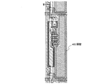
図1に、本発明の発光素子の素子構成の一例の模式図を示す。本実施の形態における発光素子の構造は、一対(陽極、及び陰極)の電極間に発光層を有するものとする。なお、素子構造についてはこれに限らず、目的に応じて、周知の構造を適宜選択すればよい。 FIG. 1 shows a schematic diagram of an example of the element structure of the light-emitting element of the present invention. In the structure of the light-emitting element in this embodiment, a light-emitting layer is provided between a pair of (anode and cathode) electrodes. Note that the element structure is not limited to this, and a known structure may be appropriately selected according to the purpose.
図1は、第1の電極101と第2の電極102との間に発光層113を有する発光素子の一例を示す。そして、発光層113は、本発明のアントラセン誘導体を含む。また、第1の電極101及び第2の電極102のいずれか一方は陽極となり、他方は陰極となる。本発明において、陽極とは発光層に正孔を注入する電極のことを示し、陰極とは発光層に電子を注入する電極のことを示す。なお、本実施の形態では第1の電極101を陽極とし、第2の電極102を陰極とする。
FIG. 1 illustrates an example of a light-emitting element having a light-emitting
本実施の形態の発光素子において、第1の電極101側から注入された正孔と、第2の電極102側から注入された電子とが発光層113において再結合し、本発明のアントラセン誘導体を励起状態にする。そして、励起状態の本発明のアントラセン誘導体は基底状態に戻る時に発光する。本発明のアントラセン誘導体は発光物質として機能する。なお、発光物質とは、励起状態から基底状態に戻る時に発光し、発光量子効率が良好で、所望の発光波長の発光を呈し得る物質である。
In the light-emitting element of this embodiment mode, holes injected from the first electrode 101 side and electrons injected from the
また、本実施の形態の発光素子は、第1の電極101と発光層113との間に、正孔注入層111と正孔輸送層112とが順に積層されて設けられている構造とする。本発明において、正孔注入層111は、第1の電極101側から正孔輸送層112へ正孔の注入を補助する機能を有する層を示す。このように正孔注入層111を設けることによって、第1の電極101と正孔輸送層112との間のイオン化ポテンシャルの差が緩和され、正孔が注入され易くなり、その結果、発光素子の駆動電圧を低減することができる。また、正孔輸送層112は、第1の電極101側から注入された正孔を発光層113へ輸送する機能を有する層を示す。このように正孔輸送層112を設けることによって、第1の電極101と発光層113との距離を離すことができ、その結果、第1の電極101等に含まれている金属に起因して発光が消光することを防ぐことができる。
In addition, the light-emitting element of this embodiment has a structure in which the hole injection layer 111 and the
さらに、本実施の形態の発光素子は、発光層113と第2の電極102との間に、電子輸送層114と電子注入層115とが順に積層されて設けられている構造とする。本発明において、電子輸送層114は、第2の電極102側から注入された電子を発光層113へ輸送する機能を有する層を示す。このように、電子輸送層114を設けることによって、第2の電極102と発光層113との距離を離すことができ、その結果、第2の電極102等に含まれている金属に起因して発光が消光することを防ぐことができる。また、電子注入層115は、第2の電極102側から電子輸送層114へ電子の注入を補助する機能を有する層を示す。このように、電子注入層を設けることによって、第2の電極102と電子輸送層114との間の電子親和力の差が緩和され、電子が注入され易くなり、その結果、発光素子の駆動電圧を低減することができる。
Further, the light-emitting element of this embodiment has a structure in which an electron-transport layer 114 and an electron-injection layer 115 are sequentially stacked between the light-emitting
以下、第1の電極101、第2の電極102、及び第1の電極101と第2の電極102との間に位置する各層について、具体的に説明する。
Hereinafter, the first electrode 101, the
陽極(第1の電極101)としては、公知の材料を用いることができるが、仕事関数の大きい(具体的には4.0eV以上)金属、合金、導電性化合物、およびこれらの混合物などを用いるのが好ましい。具体的には、透光性を有する導電性材料からなる透明導電層を用いればよく、酸化タングステンを含むインジウム酸化物、酸化タングステンを含むインジウム亜鉛酸化物、酸化チタンを含むインジウム酸化物、酸化チタンを含むインジウム錫酸化物などを用いることができる。また、インジウム錫酸化物(ITO)、インジウム亜鉛酸化物(IZO)、酸化ケイ素を添加したインジウム錫酸化物(ITSO)なども用いることができる。その他、金(Au)、白金(Pt)、ニッケル(Ni)、タングステン(W)、クロム(Cr)、亜鉛(Zn)、スズ(Sn)、インジウム(In)、モリブデン(Mo)、鉄(Fe)、コバルト(Co)、銅(Cu)、パラジウム(Pd)から選ばれた元素、または前記元素を主成分とする合金材料、例えば窒化チタン(TiN)、窒化珪素チタン(TiSiXNY)、珪化タングステン(WSiX)、窒化タングステン(WNX)、窒化珪化タングステン(WSiXNY)、窒化ニオブ(NbN)等を用いることができる。なお、陽極は、これらの材料の単層膜または積層膜を、スパッタリング法や蒸着法などの方法を用いて形成すればよい。また、導電性材料を用いる場合、ゾル−ゲル法などを応用して作製しても構わない。 A known material can be used for the anode (first electrode 101), but a metal, an alloy, a conductive compound, a mixture thereof, or the like having a high work function (specifically, 4.0 eV or more) is used. Is preferred. Specifically, a transparent conductive layer made of a light-transmitting conductive material may be used. Indium oxide containing tungsten oxide, indium zinc oxide containing tungsten oxide, indium oxide containing titanium oxide, titanium oxide Indium tin oxide containing can be used. Indium tin oxide (ITO), indium zinc oxide (IZO), indium tin oxide to which silicon oxide is added (ITSO), or the like can also be used. In addition, gold (Au), platinum (Pt), nickel (Ni), tungsten (W), chromium (Cr), zinc (Zn), tin (Sn), indium (In), molybdenum (Mo), iron (Fe ), Cobalt (Co), copper (Cu), palladium (Pd), or an alloy material containing the element as a main component, for example, titanium nitride (TiN), silicon titanium nitride (TiSi X N Y ), Tungsten silicide (WSi X ), tungsten nitride (WN X ), tungsten nitride silicide (WSi X N Y ), niobium nitride (NbN), or the like can be used. Note that the anode may be formed using a single-layer film or a stacked-layer film of these materials by a method such as a sputtering method or an evaporation method. In the case of using a conductive material, a sol-gel method or the like may be applied.
また、各透光性を有する導電性材料の、組成比の例を述べる。例えば、酸化タングステンを含むインジウム酸化物の組成比は、酸化タングステン1.0wt%、インジウム酸化物99.0wt%とすればよい。酸化タングステンを含むインジウム亜鉛酸化物の組成比は、酸化タングステン1.0wt%、酸化亜鉛0.5wt%、インジウム酸化物98.5wt%とすればよい。酸化チタンを含むインジウム酸化物の組成比は、酸化チタン1.0wt%〜5.0wt%、インジウム酸化物99.0wt%〜95.0wt%とすればよい。インジウム錫酸化物(ITO)の組成比は、酸化錫10.0wt%、インジウム酸化物90.0wt%とすればよい。インジウム亜鉛酸化物(IZO)の組成比は、酸化亜鉛10.7wt%、インジウム酸化物89.3wt%とすればよい。酸化チタンを含むインジウム錫酸化物の組成比は、酸化チタン5.0wt%、酸化錫10.0wt%、インジウム酸化物85.0wt%とすればよい。なお、上記組成比は例であり、適宜その組成比の割合は設定すればよい。 In addition, examples of the composition ratio of each light-transmitting conductive material will be described. For example, the composition ratio of indium oxide containing tungsten oxide may be 1.0 wt% tungsten oxide and 99.0 wt% indium oxide. The composition ratio of indium zinc oxide containing tungsten oxide may be 1.0 wt% tungsten oxide, 0.5 wt% zinc oxide, and 98.5 wt% indium oxide. The composition ratio of indium oxide containing titanium oxide may be 1.0 wt% to 5.0 wt% titanium oxide and 99.0 wt% to 95.0 wt% indium oxide. The composition ratio of indium tin oxide (ITO) may be 10.0 wt% tin oxide and 90.0 wt% indium oxide. The composition ratio of indium zinc oxide (IZO) may be 10.7 wt% zinc oxide and 89.3 wt% indium oxide. The composition ratio of indium tin oxide containing titanium oxide may be 5.0 wt% titanium oxide, 10.0 wt% tin oxide, and 85.0 wt% indium oxide. In addition, the said composition ratio is an example, What is necessary is just to set the ratio of the composition ratio suitably.
陰極(第2の電極102)としては、公知の材料を用いることができるが、仕事関数の小さい(具体的には3.8eV以下)金属、合金、導電性化合物、およびこれらの混合物などを用いることが好ましい。具体的には、元素周期表の1族または2族に属する金属、すなわちリチウム(Li)やセシウム(Cs)等のアルカリ金属、およびマグネシウム(Mg)、カルシウム(Ca)、ストロンチウム(Sr)等のアルカリ土類金属、およびこれらを含む合金(MgとAgの合金、AlとLiの合金等)、ユウロピウム(Er)、イッテルビウム(Yb)等の希土類金属およびこれらを含む合金などを用いることができる。ただし、高い電子注入性を有する電子注入層を用いることにより、仕事関数の高い材料、すなわち、通常は陽極に用いられている材料で陰極を形成することもできる。例えば、Al、Ag、ITO等の金属・導電性無機化合物により陰極を形成することもできる。なお、陰極は、これらの単層膜または積層膜を、スパッタリング法や蒸着法などの方法を用いて形成すればよい。
As the cathode (second electrode 102), a known material can be used, but a metal, an alloy, a conductive compound, a mixture thereof, or the like having a low work function (specifically, 3.8 eV or less) is used. It is preferable. Specifically, metals belonging to
正孔注入層111としては、正孔輸送層112を形成している物質よりもイオン化ポテンシャルが小さく、第1の電極101を形成している物質よりもイオン化ポテンシャルが大きい物質、または正孔輸送層112と第1の電極101との間に1〜2nmの薄膜として設けたときにエネルギーバンドが曲がるような物質を用いて形成することが好ましい。正孔注入層111を形成するのに用いることのできる物質の具体例として、フタロシアニン(略称:H2Pc)や銅フタロシアニン(CuPc)等のフタロシアニン系の化合物、或いはポリ(エチレンジオキシチオフェン)/ポリ(スチレンスルホン酸)水溶液(PEDOT/PSS)等の高分子等が挙げられる。つまり、正孔注入層111におけるイオン化ポテンシャルが正孔輸送層112におけるイオン化ポテンシャルよりも相対的に小さくなるような物質を正孔輸送性物質の中から選択することによって、正孔注入層111を形成することができる。なお、正孔輸送性物質とは、電子よりも正孔の移動度が高く、電子の移動度に対する正孔の移動度の比の値(=正孔移動度/電子移動度)が好ましくは100よりも大きい物質をいう。また、正孔注入層111を設ける場合、第1の電極101は、インジウム錫酸化物等の仕事関数の高い物質を用いて形成することが好ましい。
As the hole injection layer 111, a substance having a lower ionization potential than the substance forming the
正孔輸送層112としては、正孔輸送性物質を用いて形成することが好ましく、特に1×10−6cm2/Vs以上の正孔移動度を有する物質を用いて形成することが好ましい。正孔輸送層112を形成するのに用いることができる物質の具体例としては、4,4’−ビス[N−(1−ナフチル)−N−フェニルアミノ]ビフェニル(略称:NPB)、4,4’−ビス[N−(3−メチルフェニル)−N−フェニルアミノ]ビフェニル(略称:TPD)、4,4’,4’’−トリス(N,N−ジフェニルアミノ)トリフェニルアミン(略称:TDATA)、4,4’,4’’−トリス[N−(3−メチルフェニル)−N−フェニルアミノ]トリフェニルアミン(略称:MTDATA)、4,4’−ビス{N−[4−(N,N−ジ−m−トリルアミノ)フェニル]−N−フェニルアミノ}ビフェニル(略称:DNTPD)、1,3,5−トリス[N,N−ジ(m−トリル)アミノ]ベンゼン(略称:m−MTDAB)、4,4’,4’’−トリス(N−カルバゾリル)トリフェニルアミン(略称:TCTA)、フタロシアニン(略称:H2Pc)、銅フタロシアニン(略称:CuPc)、バナジルフタロシアニン(略称:VOPc)、4,4’−ビス[N−(4−ビフェニリル)−N−フェニルアミノ]ビフェニル(略称:BBPB)等が挙げられる。なお、正孔輸送性物質の中でも特にホストとして用いられる物質よりもエネルギーギャップの大きい物質を選択して正孔輸送層112を形成することがより好ましい。また、正孔輸送層112は、以上に述べた物質を用いて形成された層を二以上組み合わせて形成した多層構造の層であってもよい。
The
発光層113としては、実施の形態1に記載の本発明のアントラセン誘導体のうち、一種類のアントラセン誘導体のみを含む単層膜を用いることができる。また、実施の形態1に記載の本発明のアントラセン誘導体が、各アントラセン誘導体の有するエネルギーギャップよりも大きいエネルギーギャップを有し、また各アントラセン誘導体の有するイオン化ポテンシャルよりも大きいイオン化ポテンシャルを有する物質(ホストと称される)を主成分とする層中に、分散して含まれた層を用いることもできる。本発明のアントラセン誘導体を、ホストを主成分とする層中に分散させることによって、各アントラセン誘導体からの発光が、各アントラセン誘導体自体の濃度に起因して消光してしまうことを防ぐことができる。なお、エネルギーギャップとはLUMO準位とHOMO準位との間のエネルギーギャップをいう。
As the light-emitting
より具体的には、ホストとして用いる物質は、正孔よりも電子の輸送性が高い物質であることが好ましい。このような物質として、例えば、2−tert−ブチル−9、10−ジ(2−ナフチル)アントラセン(略称:t−BuDNA)、9−[4−(N−カルバゾリル)]フェニル−10−フェニルアントラセン(略称:CzPA)、及びジフェニルアントラセン等のアントラセン誘導体、バソキュプロイン(略称:BCP)等のフェナントロリン誘導体、オキサジアゾール誘導体、トリアジン誘導体が挙げられる。これらの物質の中から一または二以上の物質を選択し、実施の形態1に記載の本発明のアントラセン誘導体が分散状態となるように混合すればよい。発光層113をこのような構成とすることによって、実施の形態1に記載の本発明のアントラセン誘導体に効率良く正孔をトラップさせることができ、その結果、発光効率の良い発光素子を得ることができる。また、電子輸送層114はエネルギーギャップの小さい物質で形成されることが多く、発光層113から励起エネルギーが移動し易いが、発光層113を以上のような構成とすることによって、発光層113における正孔と電子の再結合領域(発光領域)が正孔輸送層112側に形成されるようになり、電子輸送層114への励起エネルギーの移動を防ぐことができる。その結果、発光層113と異なる層において発光が生じることに起因した色度の低下を防ぐことができる。なお、発光層113を複数の化合物が混合された層(例えば、本発明のアントラセン誘導体を、ホストを主成分とする層中に分散させた層)とする場合は、共蒸着法を用いて形成すればよい。ここで、共蒸着とは、一つの処理室内に設けられた複数の蒸着源からそれぞれ原料を気化させ、気化した原料を気相状態で混合し、被処理物上に堆積させる蒸着法をいう。
More specifically, the substance used as the host is preferably a substance having a higher electron transporting property than holes. As such a substance, for example, 2-tert-butyl-9,10-di (2-naphthyl) anthracene (abbreviation: t-BuDNA), 9- [4- (N-carbazolyl)] phenyl-10-phenylanthracene (Abbreviation: CzPA), anthracene derivatives such as diphenylanthracene, phenanthroline derivatives such as bathocuproin (abbreviation: BCP), oxadiazole derivatives, and triazine derivatives. One or more substances may be selected from these substances and mixed so that the anthracene derivative of the present invention described in
電子輸送層114としては、電子輸送性物質を用いて形成することが好ましく、特に1×10−6cm2/Vs以上の電子移動度を有する物質を用いて形成することが好ましい。なお、電子輸送性物質とは、正孔よりも電子の移動度が高く、正孔の移動度に対する電子の移動度の比の値(=電子移動度/正孔移動度)が好ましくは100よりも大きい物質をいう。電子輸送層114を形成するのに用いることができる物質の具体例としては、トリス(8−キノリノラト)アルミニウム(略称:Alq3)、トリス(4−メチル−8−キノリノラト)アルミニウム(略称:Almq3)、ビス(10−ヒドロキシベンゾ[h]−キノリナト)ベリリウム(略称:BeBq2)、ビス(2−メチル−8−キノリノラト)−4−フェニルフェノラト−アルミニウム(略称:BAlq)、ビス[2−(2−ヒドロキシフェニル)ベンゾオキサゾラト]亜鉛(略称:Zn(BOX)2)、ビス[2−(2−ヒドロキシフェニル)ベンゾチアゾラト]亜鉛(略称:Zn(BTZ)2)等の金属錯体の他、2−(4−ビフェニリル)−5−(4−tert−ブチルフェニル)−1,3,4−オキサジアゾール(略称:PBD)、1,3−ビス[5−(p−tert−ブチルフェニル)−1,3,4−オキサジアゾール−2−イル]ベンゼン(略称:OXD−7)、3−(4−tert−ブチルフェニル)−4−フェニル−5−(4−ビフェニリル)−1,2,4−トリアゾール(略称:TAZ)、3−(4−tert−ブチルフェニル)−4−(4−エチルフェニル)−5−(4−ビフェニリル)−1,2,4−トリアゾール(略称:p−EtTAZ)、バソフェナントロリン(略称:BPhen)、バソキュプロイン(略称:BCP)、4,4−ビス(5−メチルベンズオキサゾル−2−イル)スチルベン(略称:BzOs)等が挙げられる。なお、電子輸送性物質の中でも特にホストとして用いられる物質よりもエネルギーギャップの大きい物質を選択して電子輸送層114を形成することがより好ましい。また、電子輸送層114は、以上に述べた物質を用いて形成された層を二以上組み合わせて形成した多層構造の層であってもよい。 The electron transporting layer 114 is preferably formed using an electron transporting substance, and particularly preferably formed using a substance having an electron mobility of 1 × 10 −6 cm 2 / Vs or higher. Note that the electron transporting substance has higher electron mobility than holes, and the ratio of the electron mobility to the hole mobility (= electron mobility / hole mobility) is preferably from 100. Also refers to a large substance. Specific examples of a substance that can be used for forming the electron-transport layer 114 include tris (8-quinolinolato) aluminum (abbreviation: Alq 3 ), tris (4-methyl-8-quinolinolato) aluminum (abbreviation: Almq 3). ), Bis (10-hydroxybenzo [h] -quinolinato) beryllium (abbreviation: BeBq 2 ), bis (2-methyl-8-quinolinolato) -4-phenylphenolato-aluminum (abbreviation: BAlq), bis [2- In addition to metal complexes such as (2-hydroxyphenyl) benzoxazolate] zinc (abbreviation: Zn (BOX) 2 ), bis [2- (2-hydroxyphenyl) benzothiazolate] zinc (abbreviation: Zn (BTZ) 2 ) 2- (4-biphenylyl) -5- (4-tert-butylphenyl) -1,3,4-oxadiazole (approximately) Name: PBD), 1,3-bis [5- (p-tert-butylphenyl) -1,3,4-oxadiazol-2-yl] benzene (abbreviation: OXD-7), 3- (4- tert-butylphenyl) -4-phenyl-5- (4-biphenylyl) -1,2,4-triazole (abbreviation: TAZ), 3- (4-tert-butylphenyl) -4- (4-ethylphenyl) -5- (4-biphenylyl) -1,2,4-triazole (abbreviation: p-EtTAZ), bathophenanthroline (abbreviation: BPhen), bathocuproin (abbreviation: BCP), 4,4-bis (5-methylbenzoxa) And sol-2-yl) stilbene (abbreviation: BzOs). Note that it is more preferable to form the electron transport layer 114 by selecting a substance having an energy gap larger than that of a substance used as a host among electron transporting substances. The electron transport layer 114 may be a layer having a multilayer structure formed by combining two or more layers formed using the above-described substances.
電子注入層115としては、BPhen、BCP、p−EtTAZ、TAZ、BzOs等の電子輸送層114を形成するのに用いることのできる物質の中から、電子輸送層114の形成に用いる物質よりも電子親和力が相対的に大きい物質を選択して用いることによって形成することができる。また、電子注入層115には、リチウム(Li)、セシウム(Cs)等のアルカリ金属、リチウム酸化物(Li2O)、カリウム酸化物(K2O)、ナトリウム酸化物(Na2O)等のアルカリ金属の酸化物、カルシウム酸化物(CaO)、マグネシウム酸化物(MgO)等のアルカリ土類金属の酸化物、フッ化リチウム(LiF)、フッ化セシウム(CsF)等のアルカリ金属のフッ化物、フッ化カルシウム(CaF2)等のアルカリ土類金属のフッ化物、またはマグネシウム(Mg)、カルシウム(Ca)等のアルカリ土類金属等の無機物が含まれていてもよい。また、電子注入層115は以上に述べたような有機物を含む構成であってもよいし、または、LiF等のアルカリ金属のフッ化物、またはCaF2等のアルカリ土類金属のフッ化物等の無機物を用いた構成であってもよい。このようにLiF等のアルカリ金属のフッ化物、またはCaF2等のアルカリ土類金属のフッ化物等の無機物を用いて1〜2nmの薄膜として電子注入層115が設けられることによって、電子注入層115のエネルギーバンドが曲がる、或いはトンネル電流が流れることにより、第2の電極102側から電子輸送層114へ電子の注入が容易となる。
As the electron injecting layer 115, an electron transporting layer 114 such as BPhen, BCP, p-EtTAZ, TAZ, or BzOs can be used more than the material used for forming the electron transporting layer 114. It can be formed by selecting and using a substance having a relatively large affinity. The electron injection layer 115 includes an alkali metal such as lithium (Li) or cesium (Cs), lithium oxide (Li 2 O), potassium oxide (K 2 O), sodium oxide (Na 2 O), or the like. Alkali metal oxides, alkaline earth metal oxides such as calcium oxide (CaO) and magnesium oxide (MgO), and alkali metal fluorides such as lithium fluoride (LiF) and cesium fluoride (CsF) In addition, fluorides of alkaline earth metals such as calcium fluoride (CaF 2 ), or inorganic substances such as alkaline earth metals such as magnesium (Mg) and calcium (Ca) may be contained. Further, the electron injection layer 115 may be configured to include the organic material as described above, or an inorganic material such as an alkali metal fluoride such as LiF or an alkaline earth metal fluoride such as CaF 2. A configuration using may be used. As described above, the electron injection layer 115 is provided as a thin film having a thickness of 1 to 2 nm using an inorganic material such as an alkali metal fluoride such as LiF or an alkaline earth metal fluoride such as CaF 2. When the energy band is bent or a tunnel current flows, injection of electrons from the
また、本実施の形態の正孔注入層111に換えて、正孔発生層を設けてもよい。なお、正孔発生層とは、正孔を発生する層であり、正孔輸送性物質の中から選ばれた少なくとも一の物質と、正孔輸送性物質に対して電子受容性を示す物質とを混合することによって形成することができる。ここで、正孔輸送性物質としては、正孔輸送層112を形成するのに用いることのできる物質と同様の物質を用いることができる。また、電子受容性を示す物質としては、モリブデン酸化物、バナジウム酸化物、ルテニウム酸化物、レニウム酸化物等の金属酸化物を用いることができる。
Further, a hole generating layer may be provided instead of the hole injecting layer 111 in this embodiment. Note that the hole generating layer is a layer that generates holes, and is composed of at least one substance selected from hole transporting substances, and a substance that exhibits electron acceptability with respect to the hole transporting substance. Can be formed by mixing. Here, as the hole transporting substance, a substance similar to the substance that can be used to form the
また、本実施の形態の電子注入層115に換えて、電子発生層を設けてもよい。なお、電子発生層とは、電子を発生する層であり、電子輸送性物質の中から選ばれた少なくとも一の物質と、電子輸送性物質に対して電子供与性を示す物質とを混合することによって形成することができる。ここで、電子輸送性物質としては電子輸送層114を形成するのに用いることのできる物質と同様の物質を用いることができる。また、電子供与性を示す物質としては、アルカリ金属およびアルカリ土類金属の中から選ばれた物質、具体的にはリチウム(Li)、カルシウム(Ca)、ナトリウム(Na)、カリウム(K)、マグネシウム(Mg)等を用いることができる。 Further, an electron generating layer may be provided instead of the electron injecting layer 115 in this embodiment. The electron generating layer is a layer that generates electrons, and is a mixture of at least one substance selected from electron transporting substances and a substance that exhibits an electron donating property with respect to the electron transporting substance. Can be formed. Here, as the electron transporting substance, a substance similar to the substance that can be used to form the electron transporting layer 114 can be used. Moreover, as the substance exhibiting electron donating property, a substance selected from alkali metals and alkaline earth metals, specifically, lithium (Li), calcium (Ca), sodium (Na), potassium (K), Magnesium (Mg) or the like can be used.
以上で述べたような本実施の形態の発光素子の作製方法は特に限定されず、例えば、第1の電極101を形成後、その上に、正孔注入層111、正孔輸送層112、発光層113、電子輸送層114、電子注入層115を順次積層して形成し、最後に第2の電極102を形成することによって作製できる。または、第2の電極102を形成後、その上に、電子注入層115、電子輸送層114、発光層113、正孔輸送層112、正孔注入層111、を順次積層して形成し、最後に第1の電極101を形成することによって作製してもよい。なお、正孔注入層111、正孔輸送層112、発光層113、電子輸送層114、電子注入層115は、それぞれ、蒸着法、またはインクジェット法、または塗布法等の方法を用いて形成すればよい。また、第1の電極101または第2の電極102についても、スパッタリング法または蒸着法等の方法を用いて形成すればよい。
There is no particular limitation on the method for manufacturing the light-emitting element of this embodiment as described above. For example, after forming the first electrode 101, the hole-injection layer 111, the hole-
以上のような構成を有する本発明の発光素子は、本発明の発光効率が非常に良いアントラセン誘導体を用いて作製されているため、高効率化した発光素子を得ることができる。また、本発明のアントラセン誘導体を用いた発光素子は寿命が長く、低い電圧で駆動することができる。従って、本発明の発光素子は、電力効率が非常に高く、低消費電力化が達成できる。 Since the light-emitting element of the present invention having the above structure is manufactured using the anthracene derivative having very good light emission efficiency of the present invention, a highly efficient light-emitting element can be obtained. In addition, a light-emitting element using the anthracene derivative of the present invention has a long lifetime and can be driven at a low voltage. Therefore, the light-emitting element of the present invention has very high power efficiency and can achieve low power consumption.
また、本発明の発光素子は、本発明のアントラセン誘導体のようにアントラセン骨格およびアミン骨格を含む化合物を用いて作製されている為、酸化反応の繰り返しによる発光物質の性質の変化に伴った発光素子の特性変化が少なく、長期間、安定な発光を呈することができる。また、本発明のアントラセン誘導体を用いて作製されている為、非常に外部量子効率が高い素子が得られ、その結果、発光効率の高い素子が得られる。特に、低電圧で駆動することができるので、電流効率、電力効率の共に高い素子が得られる。さらに、本発明のアントラセン誘導体は青色発光を示すことができるので、電流効率、電力効率の高い青色発光素子が得られる。 In addition, since the light-emitting element of the present invention is manufactured using a compound containing an anthracene skeleton and an amine skeleton like the anthracene derivative of the present invention, the light-emitting element is accompanied by a change in the properties of the light-emitting substance due to repeated oxidation reactions. Thus, stable light emission can be exhibited for a long period of time. In addition, since the device is manufactured using the anthracene derivative of the present invention, a device with very high external quantum efficiency can be obtained, and as a result, a device with high light emission efficiency can be obtained. In particular, since it can be driven at a low voltage, an element with high current efficiency and high power efficiency can be obtained. Furthermore, since the anthracene derivative of the present invention can emit blue light, a blue light-emitting element with high current efficiency and power efficiency can be obtained.
(実施の形態3)
本実施の形態では、本発明のアントラセン誘導体をホスト(発光物質と共に発光層に含ませ、発光物質を分散状態にするための物質)として用いた発光素子について、図2を用いて説明する。なお、発光層213以外は実施の形態2と同じ構造であるので、説明は省略する。
(Embodiment 3)
In this embodiment, a light-emitting element using the anthracene derivative of the present invention as a host (a substance for including a light-emitting substance in a light-emitting layer and bringing the light-emitting substance into a dispersed state) will be described with reference to FIGS. Since the structure other than the light-emitting
本実施の形態の図2に示す発光素子は、第1の電極201と第2の電極202との間に発光層213を有する。また、第1の電極201と発光層213との間には、正孔注入層211、及び正孔輸送層212が設けられており、第2の電極202と発光層213との間には、電子注入層215、及び電子輸送層214が設けられている。なお、発光素子の構造についてはこれに限らず、目的に応じて、周知の構造を適宜選択すればよい。
The light-emitting element shown in FIG. 2 in this embodiment includes a light-emitting
本実施の形態において、発光層213としては、実施の形態1に記載されたアントラセン誘導体と、本発明のアントラセン誘導体のエネルギーギャップよりも小さなエネルギーギャップを有し、また前記アントラセン誘導体の有するイオン化ポテンシャルよりも小さいイオン化ポテンシャルを有する発光物質とが含まれている。この場合、本発明のアントラセン誘導体はホストとして機能している。発光物質としては、蛍光発光材料、燐光発光材料のどちらも用いることができるが、燐光発光材料を用いる場合は燐光発光材料の三重項準位が、本発明のアントラセン誘導体よりも低くなければならない。具体的には、クマリン誘導体、オリゴフェニレン誘導体、オキサゾール誘導体、スチルベン誘導体、キノロン誘導体、アクリドン誘導体、ピレン誘導体、フェナントレン誘導体などを用いることができる。なお、発光物質として用いることのできる物質はこの限りではなく、本発明のアントラセン誘導体のエネルギーギャップよりも小さなエネルギーギャップを有し、また前記アントラセン誘導体の有するイオン化ポテンシャルよりも小さいイオン化ポテンシャルを有する発光物質であればよい。これらの発光物質は、実施の形態1に記載の本発明のアントラセン誘導体から成る層に分散するように含まれている。このように、これらの発光物質とホストとして機能する本発明のアントラセン誘導体とを組み合わせて用いることによって、ホストからの発光が混ざり難く、発光物質に由来した発光を選択的に取り出すことのできる発光素子を得ることができる。
In this embodiment mode, the light-emitting
なお、発光層213のように複数の化合物が混合された層とする場合は、共蒸着法を用いて形成すればよい。ここで、共蒸着とは、一つの処理室内に設けられた複数の蒸着源からそれぞれ原料を気化させ、気化した原料を気相状態で混合し、被処理物上に堆積させる蒸着法をいう。
Note that in the case where a layer in which a plurality of compounds is mixed as in the light-emitting
(実施の形態4)
本実施の形態では、本発明の発光装置(EL発光装置)の一例について、図3、及び図4を用いて作製方法とともに説明する。なお、本実施の形態では、同一基板上に画素部と駆動回路部とが形成されたアクティブマトリクス型の発光装置の例について説明するが、本発明はこれに限らず、パッシブ型の発光装置に適用しても構わない。
(Embodiment 4)
In this embodiment mode, an example of a light-emitting device (EL light-emitting device) of the present invention will be described with a manufacturing method with reference to FIGS. Note that in this embodiment, an example of an active matrix light-emitting device in which a pixel portion and a driver circuit portion are formed over the same substrate is described; however, the present invention is not limited thereto, and the passive light-emitting device is used. You may apply.
まず、基板300上に下地絶縁膜301を形成する。基板300側を表示面として発光を取り出す場合、基板300としては、光透過性を有するガラス基板や石英基板を用いればよい。また、プロセス中の処理温度に耐えうる耐熱性を有する光透過性のプラスチック基板を用いてもよい。また、基板300側とは逆の面を表示面として発光を取り出す場合、前述の基板の他にシリコン基板、金属基板またはステンレス基板の表面に絶縁膜を形成したものを用いても良い。少なくともプロセス中に発生する熱に耐えうる基板を用いれば良く、本実施の形態では基板300としてガラス基板を用いる。なお、ガラス基板の屈折率は1.55前後である。
First, the
下地絶縁膜301としては、酸化珪素膜、窒化珪素膜または酸化窒化珪素膜などの絶縁膜を用い、スパッタ法やLPCVD法、プラズマCVD法等の手段により、単層又は2以上の複数層で形成する。また、基板の凹凸や、基板からの不純物拡散が問題にならないのであれば、特に下地絶縁膜を形成しなくてもよい。
As the
次いで、下地絶縁膜301上に半導体層を形成する。半導体層は、非晶質半導体膜をスパッタ法、LPCVD法、またはプラズマCVD法等により成膜した後、レーザー結晶化法、熱結晶化法、またはニッケルなどの触媒元素を用いた熱結晶化法等を用いて結晶化し、結晶質半導体膜を得る。なお、ニッケルなどの触媒元素を用いた熱結晶化法を用いる場合には、結晶化後ゲッタリングにより触媒元素を除去することが好ましい。その後、フォトリソグラフィー法により、結晶質半導体膜を所望の形状に形成する。
Next, a semiconductor layer is formed over the
次いで、半導体層を覆うゲート絶縁膜302を形成する。ゲート絶縁膜302は、プラズマCVD法またはスパッタ法を用いて珪素を含む絶縁膜を形成する。また、珪素を含む絶縁膜の単層または積層構造を形成した後にマイクロ波によるプラズマを用いた表面窒化処理を行って形成しても良い。
Next, a
次いで、ゲート絶縁膜302上にゲート電極を形成する。ゲート電極は、タングステン(W)、クロム(Cr)、タンタル(Ta)、窒化タンタル(TaN)またはモリブデン(Mo)などの高融点金属、又は高融点金属を主成分とする合金もしくは化合物等の導電材料を用いて、スパッタ法、蒸着法などの方法により形成すればよい。また、ゲート電極はこれらの導電材料の単層構造でも良いし、又は2以上の複数層としてもよい。
Next, a gate electrode is formed over the
次いで、画素部及び駆動回路部に形成されるそれぞれのトランジスタ310〜340の半導体層にn型またはp型の導電型を有する不純物領域を形成するため、不純物を添加する。添加する不純物は、それぞれのトランジスタにあわせて、適宜選択すればよい。
Next, an impurity is added in order to form an impurity region having n-type or p-type conductivity in the semiconductor layer of each of the
次いで、第1の層間絶縁膜303a、第1の層間絶縁膜303bを形成する。第1の層間絶縁膜303a、303bとしては、酸化珪素膜、窒化珪素膜または酸化窒化珪素膜などの無機絶縁膜、有機樹脂膜、またはシロキサンを含む膜を用いることができ、これら絶縁膜を単層又は2以上の複数層で形成すればよい。なお、シロキサンは、シリコン(Si)と酸素(O)との結合で骨格構造が構成される材料である。置換基として、少なくとも水素を含む有機基(例えばアルキル基、芳香族炭化水素)が用いられる。また、置換基としてフルオロ基を用いてもよい。または置換基として、少なくとも水素を含む有機基と、フルオロ基とを用いてもよい。また、無機絶縁膜を形成する場合はスパッタ法、LPCVD法、またはプラズマCVD法等を用いて、有機樹脂膜やシロキサンを含む膜を形成する場合には塗布法を用いればよい。ここでは第1の層間絶縁膜を2層の積層構造としたが、単層でもよいし、3以上の複数層としてもよい。
Next, a first
次いで、第1の層間絶縁膜303a、303bを選択的にエッチングして、半導体層に達するコンタクトホールを形成する。そして、コンタクトホールを介して半導体層に達するソース電極及びドレイン電極を形成する。ソース電極及びドレイン電極は、スパッタ法により金属膜を積層した後、フォトリソグラフィー法により、選択的に金属積層膜をエッチングして形成する。
Next, the first
以上のような工程で、画素部に配置される第1のトランジスタ310、第2のトランジスタ320、駆動回路部に配置される第3のトランジスタ330、第4のトランジスタ340が形成される。なお、本実施の形態では、オフ電流低減のために第1のトランジスタ310、第2のトランジスタ320をマルチゲート構造(直列に接続された2つ以上のチャネル形成領域を含んだ半導体層と、それぞれのチャネル形成領域に電界を印加する2つ以上のゲート電極とを有する構造)としたが、本発明はこれに限らず、シングルゲート構造としてもよい。また、駆動回路部に配置される第3のトランジスタ330、第4のトランジスタ340をシングルゲート構造としたが、本発明はこれに限らず、マルチゲート構造としてもよい。
Through the above process, the
また、第1のトランジスタ310、第3のトランジスタ330、及び第4のトランジスタ340はゲート絶縁膜302を介してゲート電極と重なる低濃度不純物領域(LDD領域)を有する構造としたが、これに限らず、LDD領域を有さない構造としてもよい。
In addition, the
また、第2のトランジスタ320は、ゲート絶縁膜302を介してゲート電極と重ならない低濃度不純物領域(LDD領域)を有する構造としたが、これに限らず、LDD領域を有さない構造としてもよい。
The
なお、駆動回路部において、第3のトランジスタ330をnチャネル型とし、第4のトランジスタ340をpチャネル型とし、該第3のトランジスタ330及び第4のトランジスタ340を相補的に接続することでCMOS回路を構成し、様々な種類の回路を実現することができる。
Note that in the driver circuit portion, the
次いで、発光素子350を形成する。まず、第1の電極351(有機発光素子の陽極、又は陰極)を形成する。なお、第1の電極351は、実施の形態2、及び実施の形態3と同様に形成すればよく、説明は省略する。
Next, the light-emitting
次いで、第1の電極351の端部を覆う隔壁層360を形成する。隔壁層360は、塗布法によってアクリル、シロキサン、レジスト、酸化珪素、またはポリイミド等の絶縁膜を形成し、得られた絶縁膜をフォトリソグラフィー法により所望の形状に形成すればよい。
Next, a
なお、図3では、第1の層間絶縁膜303a、303bのみがそれぞれのトランジスタ310〜340と発光素子350との間に形成されているが、第1の層間絶縁膜303a、303bの他、第2の層間絶縁膜が設けられた構造としてもよい。この場合、第1の電極351は第1の層間絶縁膜303a、303b及び第2の層間絶縁膜を介して第1のトランジスタ310と電気的に接続するものとする。
In FIG. 3, only the first
次いで、層352、第2の電極353(有機発光素子の陰極、又は陽極)を順次形成する。なお、該層352は実施の形態2、又は実施の形態3において説明したような本発明のアントラセン誘導体を有する発光層が含まれている。また、層352には発光層の他、正孔注入層、正孔輸送層、電子輸送層、電子注入層等が含まれていてもかまわない。層352、第2の電極353は、実施の形態2、及び実施の形態3と同様に形成すればよく、説明は省略する。
Next, a
以上のような工程で、第1の電極351、層352、第2の電極353を含む発光素子350が形成される。なお、発光素子350は、隔壁層360によって、隣接して設けられている別の発光素子と分離されている。
Through the above process, the light-emitting
次いで、封止基板380をシール材370で貼り合わせて発光素子350を封止する。即ち、発光装置は、表示領域の外周をシール材370で囲み、一対の基板300、380で封止される。なお、本実施の形態では、シール材370は端子部と駆動回路部に掛かるように設けたが、少なくとも表示領域の外周を囲むように設ければよく、端子部のみに設けてもよい。また、シール材370で囲まれた領域には充填材を充填してもよいし、乾燥した不活性ガスを充填してもよい。
Next, the sealing
最後にFPC393を異方性導電層392により公知の方法で端子電極391と貼りつけ、端子部390を形成する。なお、端子電極391は、第1の電極351と同じ工程で得られる電極を最上層に用いることが好ましい。
Finally, the
また、図4は、画素部の上面図を示しており、図4中の鎖線E−Fで切断した断面が、図3における画素部の第1のトランジスタ310の断面構造に対応している。また、図4中の鎖線M−Lで切断した断面が、図3における画素部の第2のトランジスタ320の断面構造に対応している。なお、図4中の400で示した実線は、隔壁層360の周縁を示している。なお、図3、4については本発明の発光装置の一例を示した図であり、レイアウトにより配線等は適宜変更されるものとする。
4 is a top view of the pixel portion, and a cross section taken along a chain line EF in FIG. 4 corresponds to the cross-sectional structure of the
また、発光装置において、発光装置の発光表示面は、一面または両面であってもよい。第1の電極351と第2の電極353とを透明導電層で形成した場合、発光素子350の光は、基板300及び封止基板380を通過して両側に取り出される。この場合、封止基板380や充填材は透明な材料を用いることが好ましい。
In the light emitting device, the light emitting display surface of the light emitting device may be one surface or both surfaces. In the case where the
また、第2の電極353を金属膜で形成し、第1の電極351を透明導電層で形成した場合、発光素子350の光は、基板300のみを通過して一方に取り出される構造、即ちボトムエミッション型となる。この場合、封止基板380や充填材は透明な材料を用いなくともよい。
In the case where the
また、第1の電極351を金属膜で形成し、第2の電極353を透明導電層で形成した場合、発光素子350の光は、封止基板380のみを通過して一方に取り出される構造、即ちトップエミッション型となる。この場合、基板300は透明な材料を用いなくともよい。
In the case where the
また、第1の電極351及び第2の電極353は仕事関数を考慮して材料を選択する必要がある。但し第1の電極351及び第2の電極353は、画素構成によりいずれも陽極、又は陰極となりうる。第1のトランジスタ310の極性がpチャネル型である場合、第1の電極351を陽極、第2の電極353を陰極とするとよい。また、第1のトランジスタ310の極性がnチャネル型である場合、第1の電極351を陰極、第2の電極353を陽極とすると好ましい。
In addition, it is necessary to select materials for the
また、フルカラー表示する場合、本実施の形態の画素部における等価回路図を図5に示す。図5中のトランジスタ510が図3の第1のトランジスタ310に対応しており、トランジスタ520が図3の第2のトランジスタ320に対応している。赤色を表示する画素は、トランジスタ510のドレイン領域に赤色を発光する発光素子550Rが接続され、ソース領域にはアノード側電源線(R)503Rが設けられている。また、発光素子550Rには、カソード側電源線500が設けられている。また、緑色を表示する画素は、トランジスタ510のドレイン領域に緑色を発光する発光素子550Gが接続され、ソース領域にはアノード側電源線(G)503Gが設けられている。また、青色を表示する画素は、トランジスタ510のドレイン領域に青色を発光する発光素子550Bが接続され、ソース領域にはアノード側電源線(B)503Bが設けられている。それぞれ色の異なる画素にはEL材料に応じて異なる電圧をそれぞれ印加する。
FIG. 5 shows an equivalent circuit diagram in the pixel portion of this embodiment in the case of full color display. A
また、発光装置において、画面表示の駆動方法は特に限定されず、例えば、点順次駆動方法や線順次駆動方法や面順次駆動方法などを用いればよい。代表的には、線順次駆動方法とし、時分割階調駆動方法や面積階調駆動方法を適宜用いればよい。また、発光装置のソース線に入力する映像信号は、アナログ信号であってもよいし、デジタル信号であってもよく、適宜、映像信号に合わせて駆動回路などを設計すればよい。 In the light emitting device, a driving method for screen display is not particularly limited, and for example, a dot sequential driving method, a line sequential driving method, a surface sequential driving method, or the like may be used. Typically, a line sequential driving method is used, and a time-division gray scale driving method or an area gray scale driving method may be used as appropriate. The video signal input to the source line of the light-emitting device may be an analog signal or a digital signal, and a drive circuit or the like may be designed in accordance with the video signal as appropriate.
さらに、ビデオ信号がデジタルの発光装置において、画素に入力されるビデオ信号が定電圧(CV)のものと、定電流(CC)のものとがある。ビデオ信号が定電圧のもの(CV)には、発光素子に印加される信号の電圧が一定のもの(CVCV)と、発光素子に印加される信号の電流が一定のもの(CVCC)とがある。また、ビデオ信号が定電流のもの(CC)には、発光素子に印加される信号の電圧が一定のもの(CCCV)と、発光素子に印加される信号の電流が一定のもの(CCCC)とがある。 Further, in a light emitting device in which a video signal is digital, there are a video signal input to a pixel having a constant voltage (CV) and a constant current (CC). A video signal having a constant voltage (CV) includes a signal having a constant voltage applied to the light emitting element (CVCV) and a signal having a constant current applied to the light emitting element (CVCC). . In addition, when the video signal has a constant current (CC), the signal voltage applied to the light emitting element is constant (CCCV), and the signal applied to the light emitting element has a constant current (CCCC). There is.
また、発光装置において、静電破壊防止のための保護回路(保護ダイオードなど)を設けてもよい。 In the light emitting device, a protection circuit (such as a protection diode) for preventing electrostatic breakdown may be provided.
本実施の形態のように、本発明のアントラセン誘導体を含む発光素子を有することにより、低消費電力で、高輝度の発光を有する発光装置を得ることができる。 By using the light-emitting element including the anthracene derivative of the present invention as in this embodiment mode, a light-emitting device that emits light with high power consumption and high luminance can be obtained.
(実施の形態5)
本実施の形態では、本発明の発光装置(EL発光装置)にFPCや、駆動用の駆動ICを実装する例について、図6を用いて説明する。なお、この発光表示パネルに搭載されている発光素子の有する構成は、実施の形態2又は3に示したような構成である。
(Embodiment 5)
In this embodiment, an example in which an FPC or a driving IC for driving is mounted on a light-emitting device (EL light-emitting device) of the present invention will be described with reference to FIGS. Note that the structure of the light-emitting element mounted on the light-emitting display panel is the structure described in
図6(a)に示す図は、FPC6009を4カ所の端子部6008に貼り付けた発光装置の上面図の一例を示している。基板6010上には発光素子及び薄膜トランジスタ(TFT)を含む画素部6002と、TFTを含むゲート側駆動回路6003と、TFTを含む第1の駆動回路6001とが形成されている。TFTの活性層は結晶構造を有する半導体膜で構成されており、同一基板上にこれらの回路を形成している。従って、システムオンパネル化を実現した発光装置(EL発光装置)を作製することができる。
6A illustrates an example of a top view of a light-emitting device in which an
なお、基板6010はコンタクト部以外において保護膜で覆われており、保護膜上に光触媒機能を有する物質を含む下地層が設けられている。
Note that the
また、画素部を挟むように2カ所に設けられた接続領域6007は、発光素子の第2の電極(陰極)を下層の配線とコンタクトさせるために設けている。なお、発光素子の第1の電極(陽極)は画素部6002に設けられたTFTと電気的に接続している。
In addition,
また、封止基板6004は、画素部6002および駆動回路6001、6003を囲むシール材6005、およびシール材6005に囲まれた充填材料によって基板6010と固定されている。また、透明な乾燥剤を含む充填材料を充填する構成としてもよい。また、画素部と重ならない領域に乾燥剤を配置してもよい。
Further, the sealing
なお、本実施の形態では、シール材6005を一部がTFTを含むゲート側駆動回路6003と重なるように設けているが、表示領域の外周を囲むように設ければよい。すなわち、ゲート側駆動回路6003と重ならないように設けても構わない。
Note that in this embodiment mode, the
また、図6(a)に示した構造は、比較的大きなサイズ(例えば対角4.3インチ)の発光装置で好適な例を示したが、図6(b)は、狭額縁化させた小型サイズ(例えば対角1.5インチ)で好適なCOG方式を採用した例である。 In addition, the structure shown in FIG. 6A is a preferable example of a light emitting device having a relatively large size (for example, 4.3 inches diagonal), but FIG. 6B has a narrow frame. This is an example of adopting a COG method suitable for a small size (for example, a diagonal of 1.5 inches).
図6(b)において、基板6610上に駆動IC6601が実装され、駆動IC6601の先に配置された端子部6608にFPC6609を実装している。実装される駆動IC6601は、生産性を向上させる観点から、一辺が300mmから1000mm以上の矩形状の基板上に複数個作り込むとよい。つまり、基板上に駆動回路部と入出力端子を一つのユニットとする回路パターンを複数個形成し、最後に分割して駆動ICを個別に取り出せばよい。駆動ICの長さは、画素部の一辺の長さや画素ピッチを考慮して、長辺が15〜80mm、短辺が1〜6mmの矩形状に形成してもよいし、画素領域の一辺、又は画素部の一辺と各駆動回路の一辺とを足した長さに形成してもよい。
In FIG. 6B, a
駆動ICのICチップに対する外形寸法の優位性は長辺の長さにあり、長辺が15〜80mmで形成された駆動ICを用いると、画素部に対応して実装するのに必要な数がICチップを用いる場合よりも少なくて済み、製造上の歩留まりを向上させることができる。また、ガラス基板上に駆動ICを形成すると、母体として用いる基板の形状に限定されないので生産性を損なうことがない。これは、円形のシリコンウエハからICチップを取り出す場合と比較すると、大きな優位点である。 The advantage of the external dimensions of the driving IC over the IC chip is the length of the long side. When a driving IC having a long side of 15 to 80 mm is used, the number required for mounting corresponding to the pixel portion is obtained. This is less than when an IC chip is used, and the manufacturing yield can be improved. Further, when the driving IC is formed over the glass substrate, the shape of the substrate used as a base is not limited, and thus productivity is not impaired. This is a great advantage compared with the case where the IC chip is taken out from the circular silicon wafer.
また、TAB方式を採用してもよく、その場合は、複数のテープを貼り付けて、該テープに駆動ICを実装すればよい。COG方式の場合と同様に、単数のテープに単数の駆動ICを実装してもよく、この場合には、強度の問題から、駆動ICを固定するための金属片等を一緒に貼り付けるとよい。 Alternatively, a TAB method may be employed. In that case, a plurality of tapes may be attached and a driving IC may be mounted on the tapes. As in the case of the COG method, a single drive IC may be mounted on a single tape. In this case, a metal piece or the like for fixing the drive IC may be attached together due to strength problems. .
また、画素部6602と駆動IC6601の間に設けられた接続領域6607は、発光素子の第2の電極を下層の配線とコンタクトさせるために設けている。なお、発光素子の第1の電極は画素部6602に設けられたTFTと電気的に接続している。
A
また、封止基板6604は、画素部6602を囲むシール材6605、およびシール材6605に囲まれた充填材料によって基板6610と固定されている。
Further, the sealing
また、画素部のTFTの活性層として非晶質半導体膜を用いる場合には、駆動回路を同一基板上に形成することは困難であるため、大きなサイズであっても図6(b)の構成となる。 In the case where an amorphous semiconductor film is used as the active layer of the TFT in the pixel portion, it is difficult to form a driver circuit on the same substrate. Therefore, the structure shown in FIG. It becomes.
以上のような本発明の発光装置は、画素部を構成する発光素子として実施の形態2又は3に記載の発光素子を有しているため、信頼性が高く、低消費電力化も達成することができる。
Since the light-emitting device of the present invention as described above includes the light-emitting element described in
(実施の形態6)
本実施の形態では、パッシブ型の発光装置の例について、図7を用いて説明する。図7(a)、(b)は、それぞれ、本発明を適用したパッシブ型の発光装置の斜視図と上面図である。特に、図7(a)は、図7(b)の点線758で囲まれた部分について斜視した図である。図7(a)、(b)のそれぞれにおいて、対応するものは同一の符号を用いて表している。図7(a)において、基板751上には、複数の第1の電極752が並列に設けられている。第1の電極752それぞれの端部は、隔壁層753で覆われている。なお、図7(a)では、第1の基板751上に設けられた第1の電極752と隔壁層753とが配置されている様子を分かり易くする為に最も手前に位置している第1の電極752を覆う隔壁層については図示していないが、実際には最も手前に位置している第1の電極752においても隔壁層によって端部は覆われている。第1の電極752の上方には複数の第2の電極755が、第1の電極752と交差するように並列に設けられている。第1の電極752と第2の電極755との間には層754が設けられている。なお、層754は、実施の形態2、又は実施の形態3において説明したような本発明のアントラセン誘導体を有する発光層が含まれている。また、層754には発光層の他、正孔注入層、正孔輸送層、電子輸送層、電子注入層等が含まれていてもかまわない。第2の電極755の上には第2の基板759が設けられている。
(Embodiment 6)
In this embodiment, an example of a passive light-emitting device is described with reference to FIGS. FIGS. 7A and 7B are a perspective view and a top view, respectively, of a passive light emitting device to which the present invention is applied. In particular, FIG. 7A is a perspective view of a portion surrounded by a dotted
図7(b)に表されるように、第1の電極752は第1の駆動回路756に接続し、第2の電極755は第2の駆動回路757に接続している。第1の電極752と第2の電極755とが交差した部分は、電極間に発光層を挟んでなる本発明の発光素子を構成している。そして、第1の駆動回路756および第2の駆動回路757からの信号によって選択された本発明の発光素子が発光する。発光は、第1の電極752及び/又は第2の電極755を介して外部へ取り出される。そして、複数の発光素子からの発光が組み合わさり映像が映し出される。なお、図7(b)では、第1の電極752及び第2の電極755それぞれの配置を分かり易くする為に隔壁層753及び第2の基板759については図示していないが、図7(a)に表されているように、実際にはこれらも設けられている。
As shown in FIG. 7B, the
第1の電極752、第2の電極755を形成する材料については特に限定はないが、いずれか一方の電極若しくは両方の電極が、可視光を透過できるように透明導電材料を用いて形成されていることが好ましい。また、第1の基板751及び第2の基板759の材質についても特に限定はなく、それぞれガラス基板等の他、プラスチック等の樹脂を用いての可撓性を有する材料を用いて形成されていてもよい。隔壁層753についても特に限定はなく、無機物若しくは有機物のいずれかを用いて形成されていてもよいし、若しくは無機物と有機物の両方を用いて形成されていてもよい。この他、シロキサンを用いて隔壁層753が形成されていてもよい。
There is no particular limitation on the material for forming the
なお、層754は、異なる色の発光を呈する発光素子ごとに独立して設けられていてもよい。例えば、赤、緑、青のそれぞれを発光する発光素子ごとに別に層754を設けることによって多色表示が可能な発光装置を得ることができる。
Note that the
本実施の形態のように、本発明のアントラセン誘導体を含む発光層を有することにより、低消費電力で、高輝度の発光を有するパッシブ型の発光装置を得ることができる。 By including the light-emitting layer including the anthracene derivative of the present invention as in this embodiment mode, a passive light-emitting device that emits light with high power consumption and high luminance can be obtained.
(実施の形態7)
本発明の発光装置、及び電子機器として、ビデオカメラ、デジタルカメラ、ゴーグル型ディスプレイ(ヘッドマウントディスプレイ)、ナビゲーションシステム、音響再生装置(カーオーディオ、オーディオコンポ等)、ノート型パーソナルコンピュータ、ゲーム機器、携帯情報端末(モバイルコンピュータ、携帯電話、携帯型ゲーム機又は電子書籍等)、記録媒体を備えた画像再生装置(具体的にはDigital Versatile Disc(DVD)等の記録媒体を再生し、その画像を表示しうるディスプレイを備えた装置)などが挙げられる。それら電子機器の具体例を図8及び図9に示す。
(Embodiment 7)
As a light emitting device and an electronic device of the present invention, a video camera, a digital camera, a goggle type display (head mounted display), a navigation system, a sound reproduction device (car audio, audio component, etc.), a notebook personal computer, a game device, a mobile phone An information terminal (mobile computer, mobile phone, portable game machine, electronic book, etc.), an image playback device (specifically, a digital versatile disc (DVD)) provided with a recording medium, and the image is displayed. And a device equipped with a display that can be used. Specific examples of these electronic devices are shown in FIGS.
図8(a)はデジタルカメラであり、本体2101、表示部2102、撮像部、操作キー2104、シャッター2106等を含む。なお、図8(a)は表示部2102側からの図であり、撮像部は示していない。本発明により、長期間に渡って良好な表示を行うことができる表示部を有し、且つ、信頼性の高いデジタルカメラが実現できる。また、低消費電力化も達成することができる。
FIG. 8A illustrates a digital camera, which includes a
図8(b)はノート型パーソナルコンピュータであり、本体2201、筐体2202、表示部2203、キーボード2204、外部接続ポート2205、ポインティングマウス2206等を含む。本発明により、長期間に渡って良好な表示を行うことができる表示部を有し、且つ、信頼性の高いノート型パーソナルコンピュータを実現することができる。また、低消費電力化も達成することができる。
FIG. 8B shows a notebook personal computer, which includes a
図8(c)は記録媒体を備えた携帯型の画像再生装置(具体的にはDVD再生装置)であり、本体2301、筐体2302、表示部A2303、表示部B2304、記録媒体(DVD等)読み込み部2305、操作キー2306、スピーカー部2307等を含む。表示部A2303は主として画像情報を表示し、表示部B2304は主として文字情報を表示する。なお、記録媒体を備えた画像再生装置には家庭用ゲーム機器なども含まれる。本発明により、長期間に渡って良好な表示を行うことができる表示部を有し、且つ、信頼性の高い画像再生装置を実現することができる。また、低消費電力化も達成することができる。
FIG. 8C shows a portable image reproducing apparatus (specifically, a DVD reproducing apparatus) provided with a recording medium, which includes a
また、図8(d)は発光装置であり、筐体2401、支持台2402、表示部2403、スピーカ2404、ビデオ入力端子2405などを含む。この発光装置は、本発明の発光素子をその表示部2403に有する。なお、発光装置としては、具体的にはコンピュータ用、テレビ受信用、広告表示用などの全ての情報表示用の表示装置が含まれる。本発明により、長期間に渡って良好な表示を行うことができる表示部を有し、且つ、信頼性の高い発光装置を実現することができる。また、低消費電力化も達成することができる。
FIG. 8D illustrates a light-emitting device, which includes a
図9で示す携帯電話機は、操作スイッチ類3004、マイクロフォン3005などが備えられた本体(a)3001と、表示パネル(a)3008、表示パネル(b)3009、スピーカ3006などが備えられた本体(b)3002とが、蝶番3010で開閉可能に連結されている。表示パネル(a)3008と表示パネル(b)3009は、回路基板3007と共に本体(b)3002の筐体3003の中に収納される。表示パネル(a)3008及び表示パネル(b)3009の画素部は筐体3003に形成された開口窓から視認できるように配置される。
The mobile phone shown in FIG. 9 includes a main body (a) 3001 provided with
表示パネル(a)3008と表示パネル(b)3009は、その携帯電話機3000の機能に応じて画素数などの仕様を適宜設定することができる。例えば、表示パネル3008(a)を主画面とし、表示パネル(b)3009を副画面として組み合わせることができる。
In the display panel (a) 3008 and the display panel (b) 3009, specifications such as the number of pixels can be set as appropriate in accordance with the function of the
また、アンテナ3011で映像信号や音声信号等の信号を受信することにより、表示パネル(a)3008をテレビ受像器などの表示媒体として機能させてもよい。
Alternatively, the display panel (a) 3008 may function as a display medium such as a television receiver by receiving a signal such as a video signal or an audio signal with the
本発明により、長期間に渡って良好な表示を行うことができる表示部を有し、且つ、信頼性の高い携帯情報端末を実現することができる。また、低消費電力化も達成することができる。 According to the present invention, a highly reliable portable information terminal having a display portion that can perform good display over a long period of time can be realized. In addition, low power consumption can be achieved.
本実施の形態に係る携帯電話機は、その機能や用途に応じてさまざまな態様に変容し得る。例えば、蝶番3010の部位に撮像素子を組み込んで、カメラ付きの携帯電話機としても良い。また、操作スイッチ類3004、表示パネル(a)3008、表示パネル(b)3009を一つの筐体内に納めた構成としても、上記した作用効果を奏することができる。また、表示部を複数個そなえた情報表示端末に本実施の形態の構成を適用しても、同様な効果を得ることができる。
The mobile phone according to the present embodiment can be transformed into various modes depending on the function and application. For example, a mobile phone with a camera may be provided by incorporating an image sensor at the
以上の様に、本発明の発光素子を有する発光装置を搭載した、信頼性の高い様々な電子機器を完成させることができる。また、電子機器の低消費電力化も達成することができる。 As described above, various highly reliable electronic devices equipped with a light-emitting device including the light-emitting element of the present invention can be completed. In addition, low power consumption of the electronic device can be achieved.
(合成例1)
本発明のアントラセン誘導体の一例として構造式(17)で表される化合物、9−フェニル−10−[(4−[N−フェニル]−4−[3−(9−フェニルカルバゾリル)])アミノ]アントラセン(略称:PCAPA)の合成方法について説明する。
(Synthesis Example 1)
As an example of the anthracene derivative of the present invention, a compound represented by the structural formula (17), 9-phenyl-10-[(4- [N-phenyl] -4- [3- (9-phenylcarbazolyl)]) A method for synthesizing amino] anthracene (abbreviation: PCAPA) will be described.
[ステップ1:9−フェニル−10−(4−ブロモフェニル)アントラセン(略称:PA)の合成方法]
(1)9−フェニルアントラセンの合成。
9−ブロモアントラセン5.4g(21.1mmol)、フェニルボロン酸2.6g(21.1mmol)、酢酸パラジウム(II)(略称:Pd(OAc)2)60mg(0.21mmol)、炭酸カリウム水溶液(2mol/L)10mL(20mmol)、トリス(オルトートリル)ホスフィン(略称:P(o−tolyl)3)263mg(0.84mmol)、1,2−ジメトキシエタン(略称:DME)20mLを200mL三口フラスコに入れ、窒素気流下で、80℃、9時間撹拌した。反応後、析出した固体を吸引ろ過で回収してから、トルエンに溶かしフロリジル、セライト、アルミナを通してろ過をした。ろ液を水、飽和食塩水で洗浄後、硫酸マグネシウムで乾燥した。混合溶液を自然ろ過し、ろ液を濃縮したところ目的物である9−フェニルアントラセンの淡褐色固体を21.5g、収率85%で得た(合成スキーム(b―1))。
[Step 1: Method for synthesizing 9-phenyl-10- (4-bromophenyl) anthracene (abbreviation: PA)]
(1) Synthesis of 9-phenylanthracene.
5.4 g (21.1 mmol) of 9-bromoanthracene, 2.6 g (21.1 mmol) of phenylboronic acid, 60 mg (0.21 mmol) of palladium (II) acetate (abbreviation: Pd (OAc) 2 ), an aqueous potassium carbonate solution ( 2 mL / L) 10 mL (20 mmol), tris (orthotolyl) phosphine (abbreviation: P (o-tolyl) 3 ) 263 mg (0.84 mmol), 1,2-dimethoxyethane (abbreviation: DME) 20 mL are placed in a 200 mL three-neck flask. The mixture was stirred at 80 ° C. for 9 hours under a nitrogen stream. After the reaction, the precipitated solid was collected by suction filtration, dissolved in toluene, and filtered through florisil, celite, and alumina. The filtrate was washed with water and saturated brine, and dried over magnesium sulfate. The mixed solution was naturally filtered, and the filtrate was concentrated to obtain 21.5 g of a light brown solid of 9-phenylanthracene, which was the object, in a yield of 85% (Synthesis scheme (b-1)).
(2)9−ブロモ−10−フェニルアントラセンの合成。
9−フェニルアントラセン6.0g(23.7mmol)を四塩化炭素80mLに溶かし、その反応溶液へ滴下ロートより、臭素3.80g(21.1mmol)を四塩化炭素10mLに溶かした溶液を滴下した。滴下終了後、室温で1時間撹拌した。反応後、チオ硫酸ナトリウム水溶液を加えて撹拌してから、有機層を水酸化ナトリウム水溶液、飽和食塩水で洗浄し、硫酸マグネシウムで乾燥した。混合溶液を自然ろ過し、ろ液を濃縮しトルエンに溶かしフロリジル、セライト、アルミナを通してろ過を行なった。ろ液を濃縮し、ジクロロメタン、ヘキサンの混合溶液により再結晶を行なったところ、目的物である9−ブロモ−10−フェニルアントラセンの淡黄色固体を7.0g、収率89%で得た。(合成スキーム(b―2))。
(2) Synthesis of 9-bromo-10-phenylanthracene.
6.0 g (23.7 mmol) of 9-phenylanthracene was dissolved in 80 mL of carbon tetrachloride, and a solution of 3.80 g (21.1 mmol) of bromine in 10 mL of carbon tetrachloride was added dropwise to the reaction solution from the dropping funnel. After completion of dropping, the mixture was stirred at room temperature for 1 hour. After the reaction, an aqueous sodium thiosulfate solution was added and stirred, and then the organic layer was washed with an aqueous sodium hydroxide solution and saturated brine and dried over magnesium sulfate. The mixed solution was naturally filtered, the filtrate was concentrated, dissolved in toluene, and filtered through florisil, celite, and alumina. The filtrate was concentrated and recrystallized with a mixed solution of dichloromethane and hexane. As a result, 7.0 g of a light yellow solid of 9-bromo-10-phenylanthracene as a target substance was obtained in a yield of 89%. (Synthesis scheme (b-2)).
(3)9−ヨード−10−フェニルアントラセンの合成。
9−ブロモ−10−フェニルアントラセン3.33g(10mmol)をテトラヒドロフラン(略称:THF)80mLに溶かし、−78℃にしてから、その反応溶液へ滴下ロートより、n−ブチルリチウム(略称:n−BuLi)(1.6mol/L ヘキサン溶液)7.5mL(12.0mmol)を滴下し、1時間撹拌した。ヨウ素5g(20.0mmol)をTHF20mLに溶かした溶液を滴下し、−78℃でさらに2時間撹拌した。反応後、チオ硫酸ナトリウム水溶液を加えて撹拌してから、有機層をチオ硫酸ナトリウム水溶液、飽和食塩水で洗浄し、硫酸マグネシウムで乾燥した。混合溶液を自然ろ過し、ろ液を濃縮し、得られた固体をエタノールにより再結晶したところ目的物である9−ヨード−10−フェニルアントラセンの淡黄色固体を3.1g、収率83%で得た(合成スキーム(b―3))。
(3) Synthesis of 9-iodo-10-phenylanthracene.
After dissolving 3.33 g (10 mmol) of 9-bromo-10-phenylanthracene in 80 mL of tetrahydrofuran (abbreviation: THF) and setting to −78 ° C., n-butyllithium (abbreviation: n-BuLi) is added to the reaction solution from the dropping funnel. ) (1.6 mol / L hexane solution) 7.5 mL (12.0 mmol) was added dropwise and stirred for 1 hour. A solution prepared by dissolving 5 g (20.0 mmol) of iodine in 20 mL of THF was added dropwise, and the mixture was further stirred at −78 ° C. for 2 hours. After the reaction, an aqueous sodium thiosulfate solution was added and stirred, and then the organic layer was washed with an aqueous sodium thiosulfate solution and saturated brine, and dried over magnesium sulfate. The mixed solution was naturally filtered, the filtrate was concentrated, and the obtained solid was recrystallized with ethanol. As a result, 3.1 g of a light yellow solid of 9-iodo-10-phenylanthracene, which was the target product, was obtained in a yield of 83%. Obtained (Synthesis scheme (b-3)).
(4)9−フェニル−10−(4−ブロモフェニル)アントラセン(略称:PA)の合成。
9−ヨード−10−フェニルアントラセン1.0g(2.63mmol)、p−ブロモフェニルボロン酸542mg(2.70mmol)、テトラキス(トリフェニルホスフィン)パラジウム(0)(略称:Pd(PPh3)4)46mg(0.03mmol)、炭酸カリウム水溶液(2mol/L)3mL(6mmol)、トルエン10mLの混合物を80℃、9時間撹拌した。反応後、トルエンを加えてからフロリジル、セライト、アルミナを通してろ過をした。ろ液を水、飽和食塩水で洗浄後、硫酸マグネシウムで乾燥した。混合溶液を自然ろ過し、ろ液を濃縮し、得られた固体をクロロホルム、ヘキサンの混合溶液により再結晶したところ目的物である9−フェニル−10−(4−ブロモフェニル)アントラセン(PA)の淡褐色固体を562mg、収率45%で得た(合成スキーム(b―4))。
(4) Synthesis of 9-phenyl-10- (4-bromophenyl) anthracene (abbreviation: PA).
9-iodo-10-phenylanthracene 1.0 g (2.63 mmol), p-bromophenylboronic acid 542 mg (2.70 mmol), tetrakis (triphenylphosphine) palladium (0) (abbreviation: Pd (PPh 3 ) 4 ) A mixture of 46 mg (0.03 mmol), aqueous potassium carbonate solution (2 mol / L) 3 mL (6 mmol), and
[ステップ2:3−(N−フェニルアミノ)−9−フェニルカルバゾール(略称:PCA)の合成方法]
(1)3−ブロモ−9−フェニルカルバゾールの合成。
N−フェニルカルバゾール24.3g(100mmol)を氷酢酸600mLに溶かし、N−ブロモコハク酸イミド17.8g(100mmol)をゆっくり加え、室温で約12時間撹拌した。この氷酢酸溶液を氷水1Lに撹拌しながら滴下した。析出した白色固体を水で3回洗浄した。この固体をジエチルエーテル150mLに溶解し、飽和炭酸水素ナトリウム水溶液、水で洗浄した。この有機層を硫酸マグネシウムで乾燥させた。混合溶液をろ過し、得られたろ液を濃縮した。得られた残渣をメタノールにより再結晶したところ、目的物である3−ブロモ−9−フェニルカルバゾールの白色粉末を28.4g、収率88%で得た(合成スキーム(c―1))。
[Step 2: Method for synthesizing 3- (N-phenylamino) -9-phenylcarbazole (abbreviation: PCA)]
(1) Synthesis of 3-bromo-9-phenylcarbazole.
N-phenylcarbazole (24.3 g, 100 mmol) was dissolved in glacial acetic acid (600 mL), N-bromosuccinimide (17.8 g, 100 mmol) was slowly added, and the mixture was stirred at room temperature for about 12 hours. This glacial acetic acid solution was added dropwise to 1 L of ice water with stirring. The precipitated white solid was washed 3 times with water. This solid was dissolved in 150 mL of diethyl ether and washed with a saturated aqueous sodium hydrogen carbonate solution and water. This organic layer was dried over magnesium sulfate. The mixed solution was filtered, and the obtained filtrate was concentrated. When the obtained residue was recrystallized from methanol, 28.4 g of a target white powder of 3-bromo-9-phenylcarbazole was obtained in a yield of 88% (Synthesis scheme (c-1)).
(2)3−(N−フェニルアミノ)−9−フェニルカルバゾール(PCA)の合成。
500mL三口フラスコに、3−ブロモ−9−フェニルカルバゾール19g(60mmol)、ビス(ジベンジリデンアセトン)パラジウム(0)(略称:Pd(dba)2)340mg(0.6mmol)、1,1−ビス(ジフェニルホスフィノ)フェロセン(略称:DPPF)1.6g(3.0mmol)、t−ブトキシナトリウム(略称:t−BuONa)13g(180mmol)を入れ、窒素置換してから、脱水キシレン110mL、アニリン7.0g(75mmol)を加え、90℃で7.5時間加熱撹拌した。反応終了後、反応溶液に50℃に温めたトルエンを約500mL加え、これをフロリジル、アルミナ、セライトを通してろ過した。ろ液を濃縮し、得られた固体をヘキサン、酢酸エチルの混合溶液により再結晶したところ、目的物である3−(N−フェニルアミノ)−9−フェニルカルバゾール(PCA)の淡黄色の粉末状固体を15g、収率75%で得た(合成スキーム(c−2))。
(2) Synthesis of 3- (N-phenylamino) -9-phenylcarbazole (PCA).
In a 500 mL three-necked flask, 19 g (60 mmol) of 3-bromo-9-phenylcarbazole, 340 mg (0.6 mmol) of bis (dibenzylideneacetone) palladium (0) (abbreviation: Pd (dba) 2 ), 1,1-bis ( Diphenylphosphino) ferrocene (abbreviation: DPPF) 1.6 g (3.0 mmol) and t-butoxy sodium (abbreviation: t-BuONa) 13 g (180 mmol) were added, and after nitrogen substitution,
得られたPCAの1H−NMRを以下に示す。また、1H−NMRのチャートを図28(a)に、図28(a)における5.0〜9.0ppmの範囲を拡大したチャートを図28(b)に示す。
1H−NMR(300MHz、CDCl3);δ=6.84(t、J=6.9、1H)、6.97(d、J=7.8、2H)、7.20−7.61(m、13H)、7.90(s、1H)、8.04(d、J=7.8、1H)
1 H-NMR of the obtained PCA is shown below. Further, FIG. 28A shows a 1 H-NMR chart, and FIG. 28B shows an enlarged chart of the range of 5.0 to 9.0 ppm in FIG.
1 H-NMR (300 MHz, CDCl 3 ); δ = 6.84 (t, J = 6.9, 1H), 6.97 (d, J = 7.8, 2H), 7.20-7.61. (M, 13H), 7.90 (s, 1H), 8.04 (d, J = 7.8, 1H)
また、得られたPCAの重溶媒にDMSOを用いた際の1H−NMRを以下に示す。また、1H−NMRのチャートを図29(a)に、図29(a)における6.5ppm〜8.5ppmの範囲を拡大したチャートを図29(b)に示す。
1H−NMR(300MHz、DMSO−d6);δ=6.73(t、J=7.5、1H)、7.02(d、J=8.1、2H)、7.16−7.70(m、12H)、7.95(s、1H)、8.06(s、1H)、8.17(d、J=7.8、1H)
Moreover, 1 H-NMR when DMSO is used as the heavy solvent of the obtained PCA is shown below. Further, FIG. 29A shows a 1 H-NMR chart, and FIG. 29B shows an enlarged chart of the range of 6.5 ppm to 8.5 ppm in FIG. 29A.
1 H-NMR (300 MHz, DMSO-d 6 ); δ = 6.73 (t, J = 7.5, 1H), 7.02 (d, J = 8.1, 2H), 7.16-7 .70 (m, 12H), 7.95 (s, 1H), 8.06 (s, 1H), 8.17 (d, J = 7.8, 1H)
また、得られたPCAの重溶媒にDMSOを用いた際の13C−NMRを以下に示す。また、13C−NMRチャートを図30(a)に、図30(a)における100ppm〜150ppmの範囲を拡大したチャートを図30(b)に示す。
13C−NMR(75.5MHz、DMSO−d6):δ=109.55、110.30、110.49、114.71、118.22、119.70、120.14、120.61、122.58、123.35、126.18、126.48、127.37、129.15、130.14、135.71、136.27、137.11、140.41、145.61
Moreover, 13 C-NMR when DMSO is used as the heavy solvent of the obtained PCA is shown below. A 13 C-NMR chart is shown in FIG. 30 (a), and a chart in which the range of 100 ppm to 150 ppm in FIG. 30 (a) is enlarged is shown in FIG. 30 (b).
13 C-NMR (75.5 MHz, DMSO-d 6 ): δ = 109.55, 110.30, 110.49, 114.71, 118.22, 119.70, 120.14, 120.61, 122 .58, 123.35, 126.18, 126.48, 127.37, 129.15, 130.14, 135.71, 136.27, 137.11, 140.41, 145.61
[ステップ3:9−フェニル−10−[(4−[N−フェニル]−4−[3−(9−フェニルカルバゾリル)])アミノ]アントラセン(PCAPA)の合成方法]
100mL三口フラスコに、9−フェニル−10−(4−ブロモフェニル)アントラセン(PA)409mg(1.0mmol)、3−(N−フェニルアミノ)−9−フェニルカルバゾール(PCA)339mg(1.0mmol)、Pd(dba)26mg(0.01mmol)、t−ブトキシナトリウム(略称:t−BuONa)500mg(5.2mol)、トリ(t−ブチル)ホスフィン(10wt% ヘキサン溶液)(略称:P(tBu)3)0.1mL、トルエン10mLを入れ、80℃で4時間撹拌した。反応後、溶液を水で洗浄し、水層をトルエンで抽出し、有機層と併せて飽和食塩水で洗浄後、硫酸マグネシウムで乾燥した。混合溶液を自然ろ過し、濃縮し得られた油状物をシリカゲルカラムクロマトグラフィー(ヘキサン:トルエン=7:3)により精製し、ジクロロメタン、ヘキサンの混合溶液により再結晶したところ目的物の黄色粉末状固体を534mg、収率81%で得た(合成スキーム(d―1))。この化合物を、核磁気共鳴法(NMR)によって測定し、9−フェニル−10−[(4−[N−フェニル]−4−[3−(9−フェニルカルバゾリル)])アミノ]アントラセン(PCAPA)であることを確認した。
[Step 3: Method for synthesizing 9-phenyl-10-[(4- [N-phenyl] -4- [3- (9-phenylcarbazolyl)]) amino] anthracene (PCAPA)]
In a 100 mL three-necked flask, 409 mg (1.0 mmol) of 9-phenyl-10- (4-bromophenyl) anthracene (PA), 339 mg (1.0 mmol) of 3- (N-phenylamino) -9-phenylcarbazole (PCA) , Pd (dba) 2 6 mg (0.01 mmol), t-butoxy sodium (abbreviation: t-BuONa) 500 mg (5.2 mol), tri (t-butyl) phosphine (10 wt% hexane solution) (abbreviation: P (tBu) 3 ) 0.1 mL and 10 mL of toluene were added and stirred at 80 ° C. for 4 hours. After the reaction, the solution was washed with water, the aqueous layer was extracted with toluene, combined with the organic layer, washed with saturated brine, and dried over magnesium sulfate. The mixed solution was naturally filtered and concentrated, and the resulting oil was purified by silica gel column chromatography (hexane: toluene = 7: 3) and recrystallized from a mixed solution of dichloromethane and hexane to obtain the desired yellow powdery solid. Was obtained in a yield of 81% (Synthesis scheme (d-1)). This compound was measured by nuclear magnetic resonance (NMR) to give 9-phenyl-10-[(4- [N-phenyl] -4- [3- (9-phenylcarbazolyl)]) amino] anthracene ( PCAPA).
この化合物の1H−NMRを以下に示す。また、1H−NMRチャートを図10(a)、(b)に示す。なお、図10(b)は、図10(a)のチャートの6.5ppm〜8.5ppmの範囲を拡大したものである。
1H−NMR(300MHz、CDCl3);δ=8.11−8.08(m、2H)、7.91−7.88(m、2H)、7.70−7.67(m、2H)、7.63−7.30(m、28H)
1 H-NMR of this compound is shown below. In addition, the 1 H-NMR chart is shown in FIGS. In addition, FIG.10 (b) expands the range of 6.5 ppm-8.5 ppm of the chart of Fig.10 (a).
1 H-NMR (300 MHz, CDCl 3 ); δ = 8.11-8.08 (m, 2H), 7.91-7.88 (m, 2H), 7.70-7.67 (m, 2H) ), 7.63-7.30 (m, 28H)
また、PCAPAの吸収スペクトルを図11に示す。測定には、紫外可視分光光度計(日本分光株式会社製、V550型)を用いた。図11において、横軸は波長(nm)、縦軸は強度(任意単位)を表す。また、図11において(a)は単膜状態における吸収スペクトルであり、(b)はトルエン溶液に溶解させた状態における吸収スペクトルである。また、PCAPAの発光スペクトルを図12に示す。図12において、横軸は波長(nm)、縦軸は強度(任意単位)を表す。また、図12において(a)は単膜状態における発光スペクトル(励起波長402nm)であり、(b)はトルエン溶液に溶解させた状態における発光スペクトル(励起波長370nm)である。図12から、PCAPAからの発光は、単膜状態において486nmにピークを有し、トルエン溶液中において471nmにピークを有することがわかる。そしてこれらの発光は、青色系の発光色として視認された。このように、PCAPAは、特に青色系の発光を呈する発光物質として適する物質であることが分かった。 Moreover, the absorption spectrum of PCAPA is shown in FIG. For the measurement, an ultraviolet-visible spectrophotometer (manufactured by JASCO Corporation, model V550) was used. In FIG. 11, the horizontal axis represents wavelength (nm) and the vertical axis represents intensity (arbitrary unit). In FIG. 11, (a) is an absorption spectrum in a single film state, and (b) is an absorption spectrum in a state dissolved in a toluene solution. In addition, FIG. 12 shows an emission spectrum of PCAPA. In FIG. 12, the horizontal axis represents wavelength (nm) and the vertical axis represents intensity (arbitrary unit). 12A shows an emission spectrum (excitation wavelength of 402 nm) in a single film state, and FIG. 12B shows an emission spectrum (excitation wavelength of 370 nm) in a state dissolved in a toluene solution. From FIG. 12, it can be seen that light emission from PCAPA has a peak at 486 nm in a single film state and a peak at 471 nm in a toluene solution. These luminescences were visually recognized as blue luminescent colors. Thus, it was found that PCAPA is a substance that is particularly suitable as a light-emitting substance that exhibits blue light emission.
また、得られたPCAPAを蒸着法によって成膜し、薄膜状態におけるPCAPAのイオン化ポテンシャルを、光電子分光装置(理研計器社製、AC−2)を用いて測定したところ、5.29eVであった。この結果からHOMO準位は−5.29eVであることが分かった。また、薄膜状態におけるPCAPAの吸収スペクトルを、紫外可視分光光度計(日本分光株式会社製、V550型)を用いて測定し、吸収スペクトル(図11における(a))の長波長側の吸収端の波長をエネルギーギャップ(2.74eV)とし、LUMO準位を求めたところ、LUMO準位は−2.55eVであった。 Moreover, when the obtained PCAPA was formed into a film by a vapor deposition method and the ionization potential of PCAPA in the thin film state was measured using the photoelectron spectrometer (AC-2, Riken Keiki Co., Ltd.), it was 5.29 eV. From this result, it was found that the HOMO level was −5.29 eV. In addition, the absorption spectrum of PCAPA in a thin film state was measured using an ultraviolet-visible spectrophotometer (manufactured by JASCO Corp., model V550), and the absorption spectrum ((a) in FIG. 11) of the absorption edge on the long wavelength side was measured. When the wavelength was the energy gap (2.74 eV) and the LUMO level was determined, the LUMO level was -2.55 eV.
さらに、得られたPCAPAの分解温度Tdを示差熱熱重量同時測定装置(セイコー電子株式会社製,TG/DTA 320型)により測定したところ、Tdは402℃以上であり、良好な耐熱性を示すことが分かった。
Further, the resulting decomposition temperature T d of the differential thermogravimetric simultaneous measurement device PCAPA (Seiko Instruments Inc., TG /
また、サイクリックボルタンメトリ(CV)測定により、PCAPAの酸化還元反応特性について調べた。なお測定には、電気化学アナライザー(ビー・エー・エス(株)製、型番:ALSモデル600A)を用いた。 Further, the oxidation-reduction characteristics of PCAPA were examined by cyclic voltammetry (CV) measurement. For the measurement, an electrochemical analyzer (manufactured by BAS Co., Ltd., model number: ALS model 600A) was used.
CV測定における溶液は、溶媒として脱水ジメチルホルムアミド(DMF)を用い、支持電解質である過塩素酸テトラ−n−ブチルアンモニウム(n−Bu4NClO4)を100mmol/Lの濃度となるように溶解させ、さらに測定対象であるPCAPAを1mmol/Lの濃度となるように溶解させて調製した。また、作用電極としては白金電極(ビー・エー・エス(株)製、PTE白金電極)を、補助電極としては白金電極(ビー・エー・エス(株)製、VC−3用Ptカウンター電極(5cm))を、基準電極としてはAg/Ag+電極(ビー・エー・エス(株)製、RE5非水溶媒系参照電極)をそれぞれ用いた。 The solution in the CV measurement uses dehydrated dimethylformamide (DMF) as a solvent and dissolves the supporting electrolyte tetra-n-butylammonium perchlorate (n-Bu 4 NClO 4 ) to a concentration of 100 mmol / L. Furthermore, PCAPA as a measurement target was prepared by dissolving it to a concentration of 1 mmol / L. In addition, as a working electrode, a platinum electrode (manufactured by BAS Co., Ltd., PTE platinum electrode), and as an auxiliary electrode, a platinum electrode (manufactured by BAS Inc., Pt counter electrode for VC-3 ( 5 cm)), and an Ag / Ag + electrode (manufactured by BAS Co., Ltd., RE5 nonaqueous solvent system reference electrode) was used as a reference electrode.
酸化反応特性については次のようにして調べた。基準電極に対する作用電極の電位を−0.27Vから0.70Vまで変化させた後、0.70Vから−0.27Vまで変化させる走査を1サイクルとし、100サイクル測定した。なお、CV測定のスキャン速度は0.1V/sに設定した。 The oxidation reaction characteristics were examined as follows. A scan in which the potential of the working electrode with respect to the reference electrode was changed from −0.27 V to 0.70 V and then changed from 0.70 V to −0.27 V was set as one cycle, and 100 cycles were measured. The scan speed for CV measurement was set to 0.1 V / s.
還元反応特性については次のようにして調べた。基準電極に対する作用電極の電位を−0.36Vから−2.60Vまで変化させた後、−2.60Vから−0.36Vまで変化させる走査を1サイクルとし、100サイクル測定した。なお、CV測定のスキャン速度は0.1V/sに設定した。 The reduction reaction characteristics were examined as follows. A scan in which the potential of the working electrode with respect to the reference electrode was changed from −0.36 V to −2.60 V and then changed from −2.60 V to −0.36 V was set as one cycle, and 100 cycles were measured. The scan speed for CV measurement was set to 0.1 V / s.
PCAPAの酸化反応特性について調べた結果を図13(a)に示す。また、PCAPAの還元反応特性について調べた結果を図13(b)に示す。図13(a)、(b)において、横軸は基準電極に対する作用電極の電位(V)を表し、縦軸は作用電極と補助電極との間に流れた電流値(1×10⁻⁵A)を表す。 FIG. 13A shows the result of examining the oxidation reaction characteristics of PCAPA. In addition, FIG. 13B shows the results of examining the reduction reaction characteristics of PCAPA. 13A and 13B, the horizontal axis represents the potential (V) of the working electrode with respect to the reference electrode, and the vertical axis represents the current value (1 × 10 −5 A) flowing between the working electrode and the auxiliary electrode. ).
図13(a)から酸化電位は0.47V(vs.Ag/Ag+電極)であることが分かった。また、図13(b)から還元電位は−2.26V(vs.Ag/Ag+電極)であることが分かった。また、100サイクルもの走査を繰り返しているにもかかわらず、酸化反応と還元反応のいずれについてもCV曲線のピークが明確に観測された。このことから、本発明のアントラセン誘導体は酸化還元反応、特に酸化反応に対して優れた可逆性を示す物質であることが分かった。 FIG. 13A shows that the oxidation potential is 0.47 V (vs. Ag / Ag + electrode). Further, from FIG. 13B, it was found that the reduction potential was −2.26 V (vs. Ag / Ag + electrode). Moreover, despite the repetition of scanning for 100 cycles, the peak of the CV curve was clearly observed for both the oxidation reaction and the reduction reaction. From this, it was found that the anthracene derivative of the present invention is a substance exhibiting excellent reversibility with respect to oxidation-reduction reactions, particularly oxidation reactions.
なお、PCAPAを本実施の形態に記載の方法によって合成すると、非常に収率良く合成することができる。 Note that when PCAPA is synthesized by the method described in this embodiment, it can be synthesized with a very high yield.
(合成例2)
本発明のアントラセン誘導体の一例として構造式(20)で表される化合物、9−フェニル−10−{4’−[N−フェニル−N−(9−フェニルカルバゾール−3−イル)アミノ]ビフェニル−4−イル}アントラセン(略称:PCAPBA)の合成方法について説明する。
(Synthesis Example 2)
As an example of the anthracene derivative of the present invention, a compound represented by the structural formula (20), 9-phenyl-10- {4 ′-[N-phenyl-N- (9-phenylcarbazol-3-yl) amino] biphenyl- A method for synthesizing 4-yl} anthracene (abbreviation: PCAPBA) will be described.
[ステップ1:9−[4−(4−ブロモフェニル)フェニル]−10−フェニルアントラセン(略称:PBA)の合成方法]
(1)4−(4−ブロモフェニル)フェニルボロン酸の合成。
4,4’−ジブロモビフェニル10.0g(0.032mol)を500mL三口フラスコに入れ窒素置換してから、テトラヒドロフラン200mLを加えて−80℃で攪拌した。反応溶液へn−ブチルリチウム (1.60M ヘキサン溶液)を20mL(0.032mol)を滴下し、−80℃のまま1時間攪拌してから、ホウ酸トリメチル40mL(0.060mol)を加え、室温に戻しながら1時間攪拌した。反応溶液へ塩化水素水(1.0mol/L)200mLを加えて約12時間攪拌した後、有機層を飽和炭酸水素ナトリウム水溶液、飽和食塩水で洗浄し、硫酸マグネシウムで乾燥した。反応溶液を自然濾過後、濃縮して得られた固体を酢酸エチル、ヘキサンの混合溶液により再結晶したところ、目的物である4−(4−ブロモフェニル)フェニルボロン酸の白色固体を、3.7g、収率41%で得た(合成スキーム(e―1))。
[Step 1: Synthesis Method of 9- [4- (4-Bromophenyl) phenyl] -10-Phenylanthracene (abbreviation: PBA)]
(1) Synthesis of 4- (4-bromophenyl) phenylboronic acid.
After putting 10.0 g (0.032 mol) of 4,4′-dibromobiphenyl into a 500 mL three-necked flask and replacing with nitrogen, 200 mL of tetrahydrofuran was added and stirred at −80 ° C. To the reaction solution, 20 mL (0.032 mol) of n-butyllithium (1.60 M hexane solution) was added dropwise and stirred at -80 ° C. for 1 hour, and then added with 40 mL (0.060 mol) of trimethyl borate, The mixture was stirred for 1 hour while returning to the normal temperature. After adding 200 mL of hydrogen chloride water (1.0 mol / L) to the reaction solution and stirring for about 12 hours, the organic layer was washed with a saturated aqueous sodium hydrogen carbonate solution and saturated brine, and dried over magnesium sulfate. The reaction solution was naturally filtered and then concentrated, and the solid obtained was recrystallized with a mixed solution of ethyl acetate and hexane. As a result, a white solid of 4- (4-bromophenyl) phenylboronic acid as the target product was obtained. 7 g, yield 41% (synthesis scheme (e-1)).
(2)9−[4−(4−ブロモフェニル)フェニル]−10−フェニルアントラセン(略称:PBA)の合成。
9−ヨード−10−フェニルアントラセン1.0g(2.63mmol)、4−(4−ブロモフェニル)フェニルボロン酸542mg(2.70mmol)、テトラキス(トリフェニルホスフィン)パラジウム(0)46mg(0.03mmol)、炭酸カリウム水溶液(2.0mol/L)3mL(6mmol)、トルエン10mLを80℃、9時間撹拌した。反応後、トルエンを加えてからフロリジル、セライト、アルミナを通してろ過をした。ろ液を水、飽和食塩水で洗浄後、硫酸マグネシウムで乾燥した。自然ろ過後、ろ液を濃縮し、クロロホルム、ヘキサンの混合溶液により再結晶したところ目的物である9−[4−(4−ブロモフェニル)フェニル]−10−フェニルアントラセン(PBA)の淡褐色固体を562mg、収率45%で得た(合成スキーム(e―2))。
(2) Synthesis of 9- [4- (4-bromophenyl) phenyl] -10-phenylanthracene (abbreviation: PBA).
9-iodo-10-phenylanthracene 1.0 g (2.63 mmol), 542 mg (2.70 mmol) of 4- (4-bromophenyl) phenylboronic acid, 46 mg (0.03 mmol) of tetrakis (triphenylphosphine) palladium (0) ), 3 mL (6 mmol) of potassium carbonate aqueous solution (2.0 mol / L) and 10 mL of toluene were stirred at 80 ° C. for 9 hours. After the reaction, toluene was added, followed by filtration through florisil, celite, and alumina. The filtrate was washed with water and saturated brine, and dried over magnesium sulfate. After natural filtration, the filtrate was concentrated and recrystallized with a mixed solution of chloroform and hexane. As a result, 9- [4- (4-bromophenyl) phenyl] -10-phenylanthracene (PBA), a light brown solid, was obtained. Was obtained in a yield of 45% (Synthesis scheme (e-2)).
[ステップ3:9−フェニル−10−{4’−[N−フェニル−N−(9−フェニルカルバゾール−3−イル)アミノ]ビフェニル−4−イル}アントラセン(略称:PCAPBA)の合成方法]
9−[4−(4−ブロモフェニル)フェニル]−10−フェニルアントラセン(PBA)730mg(1.5mmol)、3−(N−フェニルアミノ)−9−フェニルカルバゾール(PCA)500mg(1.5mmol)、ビス(ジベンジリデンアセトン)パラジウム(0)58mg(0.1mmol)、トリ(t−ブチル)ホスフィン(10wt% ヘキサン溶液)1mL(0.5mmol)、t−ブトキシナトリウム(t−BuONa)400mg(4.0mmol)の混合物に脱水キシレン15mLを加えた。これを窒素雰囲気下で110℃、5.5時間加熱撹拌した。反応終了後、この懸濁液にトルエン約200mLを加え、これをフロリジル、セライトを通して濾過した。得られたろ液を濃縮し、再結晶を行い、目的物である9−フェニル−10−{4’−[N−フェニル−N−(9−フェニルカルバゾール−3−イル)アミノ]ビフェニル−4−イル}アントラセン(略称:PCAPBA)の淡黄色粉末状固体を得た。さらに、再結晶のろ液を濃縮して得た混合物をシリカゲルカラムクロマトグラフィー(トルエン:ヘキサン=1:1)にて精製した。得られた化合物をヘキサンにより再結晶を行ったところ、目的物であるPCAPBAの淡黄色粉末状固体を得た。最初に得た目的物と合わせて700mgのPCAPBAを得て、収率は63%であった(合成スキーム(f−1))。この化合物を、核磁気共鳴法(NMR)によって測定し、9−フェニル−10−{4’−[N−フェニル−N−(9−フェニルカルバゾール−3−イル)アミノ]ビフェニル−4−イル}アントラセンであることを確認した。
[Step 3: Synthesis Method of 9-Phenyl-10- {4 ′-[N-Phenyl-N- (9-Phenylcarbazol-3-yl) amino] biphenyl-4-yl} anthracene (abbreviation: PCAPBA)]
9- [4- (4-Bromophenyl) phenyl] -10-phenylanthracene (PBA) 730 mg (1.5 mmol), 3- (N-phenylamino) -9-phenylcarbazole (PCA) 500 mg (1.5 mmol) Bis (dibenzylideneacetone) palladium (0) 58 mg (0.1 mmol), tri (t-butyl) phosphine (10 wt% hexane solution) 1 mL (0.5 mmol), t-butoxy sodium (t-BuONa) 400 mg (4 .0 mmol) was added with 15 mL of dehydrated xylene. This was heated and stirred at 110 ° C. for 5.5 hours under a nitrogen atmosphere. After completion of the reaction, about 200 mL of toluene was added to this suspension, and this was filtered through Florisil and Celite. The obtained filtrate was concentrated, recrystallized, and 9-phenyl-10- {4 ′-[N-phenyl-N- (9-phenylcarbazol-3-yl) amino] biphenyl-4- which was the target product. A light yellow powdery solid of IL} anthracene (abbreviation: PCAPBA) was obtained. Further, the mixture obtained by concentrating the recrystallized filtrate was purified by silica gel column chromatography (toluene: hexane = 1: 1). When the obtained compound was recrystallized with hexane, a pale yellow powdery solid of PCAPBA, which was the target product, was obtained. Combined with the initially obtained target product, 700 mg of PCAPBA was obtained, and the yield was 63% (Synthesis scheme (f-1)). This compound was measured by nuclear magnetic resonance (NMR), and 9-phenyl-10- {4 ′-[N-phenyl-N- (9-phenylcarbazol-3-yl) amino] biphenyl-4-yl} Confirmed to be anthracene.
この化合物の1H−NMRを以下に示す。また、1H−NMRチャートを図14(a)、(b)に示す。なお、図14(b)は、図14(a)のチャートの6.5ppm〜8.5ppmの範囲を拡大したものである。
1H−NMR(300MHz、CDCl3);δ=8.51−8.00(m、2H)、7.83−7.78(m、4H)、7.72−7.48(m、16H)、7.41−7.23(m、16H)
1 H-NMR of this compound is shown below. In addition, the 1 H-NMR chart is shown in FIGS. In addition, FIG.14 (b) expands the range of 6.5 ppm-8.5 ppm of the chart of Fig.14 (a).
1 H-NMR (300 MHz, CDCl 3 ); δ = 8.51-8.00 (m, 2H), 7.83-7.78 (m, 4H), 7.72-7.48 (m, 16H) ), 7.41-7.23 (m, 16H)
また、PCAPBAの吸収スペクトルを図15に示す。測定には、紫外可視分光光度計(日本分光株式会社製、V550型)を用いた。図15において、横軸は波長(nm)、縦軸は強度(任意単位)を表す。また、図15において(a)は単膜状態における吸収スペクトルであり、(b)はトルエン溶液に溶解させた状態における吸収スペクトルである。また、PCAPBAの発光スペクトルを図16に示す。図16において、横軸は波長(nm)、縦軸は強度(任意単位)を表す。また、図16において(a)は単膜状態における発光スペクトル(励起波長402nm)であり、(b)はトルエン溶液に溶解させた状態における発光スペクトル(励起波長395nm)である。図16から、PCAPBAからの発光は、単膜状態において482nmにピークを有し、トルエン溶液中において448nmにピークを有することがわかる。そしてこれらの発光は、青色系の発光色として視認された。このように、PCAPBAは、青色系の発光を呈する発光物質として適する物質であることが分かった。 Moreover, the absorption spectrum of PCAPBA is shown in FIG. For the measurement, an ultraviolet-visible spectrophotometer (manufactured by JASCO Corporation, model V550) was used. In FIG. 15, the horizontal axis represents wavelength (nm) and the vertical axis represents intensity (arbitrary unit). In FIG. 15, (a) is an absorption spectrum in a single film state, and (b) is an absorption spectrum in a state dissolved in a toluene solution. In addition, FIG. 16 shows an emission spectrum of PCAPBA. In FIG. 16, the horizontal axis represents wavelength (nm) and the vertical axis represents intensity (arbitrary unit). 16A shows an emission spectrum (excitation wavelength of 402 nm) in a single film state, and FIG. 16B shows an emission spectrum (excitation wavelength of 395 nm) in a state dissolved in a toluene solution. FIG. 16 shows that the emission from PCAPBA has a peak at 482 nm in the single film state and a peak at 448 nm in the toluene solution. These luminescences were visually recognized as blue luminescent colors. Thus, it was found that PCAPBA is a substance suitable as a luminescent substance that emits blue light.
また、得られたPCAPBAを蒸着法によって成膜し、薄膜状態におけるPCAPBAのイオン化ポテンシャルを、光電子分光装置(理研計器社製、AC−2)を用いて測定したところ、5.29eVであった。この結果からHOMO準位は−5.29eVであることが分かった。また、薄膜状態におけるPCAPBAの吸収スペクトルを、紫外可視分光光度計(日本分光株式会社製、V550型)を用いて測定し、吸収スペクトル(図15における(a))の長波長側の吸収端の波長をエネルギーギャップ(2.82eV)とし、LUMO準位を求めたところ、LUMO準位は−2.47eVであった。 Moreover, when the obtained PCAPBA was formed into a film by a vapor deposition method and the ionization potential of PCAPBA in the thin film state was measured using a photoelectron spectrometer (AC-2, manufactured by Riken Keiki Co., Ltd.), it was 5.29 eV. From this result, it was found that the HOMO level was −5.29 eV. Moreover, the absorption spectrum of PCAPBA in a thin film state was measured using an ultraviolet-visible spectrophotometer (manufactured by JASCO Corporation, model V550), and the absorption wavelength ((a) in FIG. 15) of the absorption edge on the long wavelength side was measured. When the wavelength was the energy gap (2.82 eV) and the LUMO level was determined, the LUMO level was -2.47 eV.
さらに、得られたPCAPBAの分解温度Tdを示差熱熱重量同時測定装置(セイコー電子株式会社製,TG/DTA 320型)により測定したところ、Tdは430℃以上であり、良好な耐熱性を示すことが分かった。
Further, the resulting decomposition temperature T d of the differential thermogravimetric simultaneous measurement device PCAPBA (Seiko Instruments Inc., TG /
なお、PCAPBAを本実施の形態に記載の方法によって合成すると、非常に収率良く合成することができる。 Note that when PCAPBA is synthesized by the method described in this embodiment, it can be synthesized with a very high yield.
(合成例3)
本発明のアントラセン誘導体の一例として、構造式(30)で表される化合物、9−{4−[N−(1−ナフチル)−N−(9−フェニルカルバゾール−3−イル)アミノ]フェニル}−10−フェニルアントラセン(略称:PCNPA)の合成方法について説明する。
(Synthesis Example 3)
As an example of the anthracene derivative of the present invention, a compound represented by the structural formula (30), 9- {4- [N- (1-naphthyl) -N- (9-phenylcarbazol-3-yl) amino] phenyl} A method for synthesizing -10-phenylanthracene (abbreviation: PCNPA) will be described.
[ステップ1:3−[N−(1−ナフチル)アミノ]−9−フェニルカルバゾール(略称:PCN)の合成方法]
窒素下で、3−ヨード−9−フェニルカルバゾール3.7g(10mmol)、1−アミノナフタレン1.6g(5 mmol)、ビス(ジベンジリデンアセトン)パラジウム(0)60mg(0.1mmol)、トリ(t−ブチル)ホスフィン(49wt% ヘキサン溶液)200μL(0.5mmol)、t−ブトキシナトリウム(略称:t−BuONa)3g(30mmol)の混合物に、脱水キシレン12mLを加えた。これを窒素雰囲気下にて90℃、7時間加熱撹拌した。反応終了後、この懸濁液に温めたトルエン約200mLを加え、これをフロリジル、アルミナ、セライトを通して濾過した。得られたろ液を濃縮し、この残渣をシリカゲルカラムクロマトグラフィー(トルエン:ヘキサン=1:1)にて分取した。得られた固体を酢酸エチル、ヘキサンの混合溶液で再結晶を行い、目的物である3−[N−(1−ナフチル)アミノ]−9−フェニルカルバゾール(PCN)のクリーム色粉末を1.5g、収率79%で得た(合成スキーム(g−1))。
[Step 1: Method for synthesizing 3- [N- (1-naphthyl) amino] -9-phenylcarbazole (abbreviation: PCN)]
Under nitrogen, 3.7 g (10 mmol) of 3-iodo-9-phenylcarbazole, 1.6 g (5 mmol) of 1-aminonaphthalene, 60 mg (0.1 mmol) of bis (dibenzylideneacetone) palladium (0), tri ( 12 mL of dehydrated xylene was added to a mixture of 200 μL (0.5 mmol) of t-butyl) phosphine (49 wt% hexane solution) and 3 g (30 mmol) of t-butoxy sodium (abbreviation: t-BuONa). This was heated and stirred at 90 ° C. for 7 hours in a nitrogen atmosphere. After completion of the reaction, about 200 mL of warm toluene was added to this suspension, and this was filtered through Florisil, alumina, and celite. The obtained filtrate was concentrated, and the residue was fractionated by silica gel column chromatography (toluene: hexane = 1: 1). The obtained solid was recrystallized with a mixed solution of ethyl acetate and hexane, and 1.5 g of cream powder of 3- [N- (1-naphthyl) amino] -9-phenylcarbazole (PCN) which is the target product was obtained. The yield was 79% (synthesis scheme (g-1)).
得られたPCNの1H−NMRを以下に示す。また、1H−NMRのチャートを図31(a)に、図31(a)における6.5〜8.5ppmの範囲を拡大したチャートを図31(b)に示す。
1H−NMR(300MHz、DMSO−d6);δ=7.13−7.71(m、15H)、7.85−7.88(m、1H)、8.03(s、1H)、8.15(d、J=7.8、1H)、8.24(s、1H)、8.36−8.39(m、1H)
1 H-NMR of the obtained PCN is shown below. In addition, FIG. 31A shows a 1 H-NMR chart, and FIG. 31B shows an enlarged chart of the range of 6.5 to 8.5 ppm in FIG.
1 H-NMR (300 MHz, DMSO-d 6 ); δ = 7.13-7.71 (m, 15H), 7.85-7.88 (m, 1H), 8.03 (s, 1H), 8.15 (d, J = 7.8, 1H), 8.24 (s, 1H), 8.36-8.39 (m, 1H)
[ステップ2:9−{4−[N−(1−ナフチル)−N−(9−フェニルカルバゾール−3−イル)アミノ]フェニル}−10−フェニルアントラセン(略称:PCNPA)の合成方法]
9−フェニル−10−(4−ブロモフェニル)アントラセン(PA)2.0g(5.0mmol)、3−[N−(1−ナフチル)アミノ]−9−フェニルカルバゾール(PCN)1.9g(5.0mmol)、t−ブトキシナトリウム(略称:t−BuONa)2.1g(20mmol)を100mL三口フラスコへ入れ、窒素置換した後、トルエン40mL、トリ(t−ブチル)ホスフィン(10wt% ヘキサン溶液)(略称:P(tBu)3)0.1mLを加えて減圧脱気した。脱気後、ビス(ジベンジリデンアセトン)パラジウム(0)30mg(0.05mmol)を加えてから、80℃で3時間撹拌した。反応後、反応溶液を、水、飽和食塩水の順に洗浄し、有機層を硫酸マグネシウムにより乾燥した。自然濾過後、ろ液を濃縮して得られた固体をシリカゲルカラムクロマトグラフィー(ヘキサン:トルエン=7:3)により精製し、目的物をジクロロメタンヘキサンにより再結晶したところ、目的物の黄色固体を1.5g、収率43%で得た(合成スキーム(g−2))。この化合物を、核磁気共鳴法(NMR)によって測定し、PCNPAであることを確認した。
[Step 2: Synthesis method of 9- {4- [N- (1-naphthyl) -N- (9-phenylcarbazol-3-yl) amino] phenyl} -10-phenylanthracene (abbreviation: PCNPA)]
9-phenyl-10- (4-bromophenyl) anthracene (PA) 2.0 g (5.0 mmol), 3- [N- (1-naphthyl) amino] -9-phenylcarbazole (PCN) 1.9 g (5 0.0 mmol) and t-butoxy sodium (abbreviation: t-BuONa) 2.1 g (20 mmol) were placed in a 100 mL three-necked flask and purged with nitrogen, followed by toluene 40 mL, tri (t-butyl) phosphine (10 wt% hexane solution) ( Abbreviation: P (tBu) 3 ) 0.1 mL was added and degassed under reduced pressure. After deaeration, 30 mg (0.05 mmol) of bis (dibenzylideneacetone) palladium (0) was added, and the mixture was stirred at 80 ° C. for 3 hours. After the reaction, the reaction solution was washed with water and saturated brine in this order, and the organic layer was dried over magnesium sulfate. After natural filtration, the solid obtained by concentrating the filtrate was purified by silica gel column chromatography (hexane: toluene = 7: 3), and the target product was recrystallized from dichloromethane hexane. 0.5 g, yield 43% (synthesis scheme (g-2)). This compound was measured by nuclear magnetic resonance (NMR) and confirmed to be PCNPA.
得られたPCNPAの1H−NMRを以下に示す。また、1H−NMRのチャートを図32(a)に、図32(a)における7.0〜8.5ppmの範囲を拡大したチャートを図32(b)に示す。
1H−NMR(300MHz,CDCl3);δ=7.13(d、J=8.7Hz、2H)、7.21−7.23(m、1H)、7.30−7.69(m、26H)、7.80−7.83(m、1H)、7.87−7.96(m、3H)、8.04(d、J=7.5Hz,1H)、8.09(d、J=2.4Hz,1H)、8.28−8.31(m、1H)
The 1 H-NMR of the obtained PCNPA is shown below. FIG. 32A shows a 1 H-NMR chart, and FIG. 32B shows an enlarged chart of the range of 7.0 to 8.5 ppm in FIG.
1 H-NMR (300 MHz, CDCl 3 ); δ = 7.13 (d, J = 8.7 Hz, 2H), 7.21-7.23 (m, 1H), 7.30-7.69 (m 26H), 7.80-7.83 (m, 1H), 7.87-7.96 (m, 3H), 8.04 (d, J = 7.5 Hz, 1H), 8.09 (d , J = 2.4 Hz, 1H), 8.28-8.31 (m, 1H)
また、PCNPAの吸収スペクトルを図33に示す。測定には、紫外可視分光光度計(日本分光株式会社製、V550型)を用いた。図33において、横軸は波長(nm)、縦軸は強度(任意単位)を表す。また、図33に示すのは、トルエン溶液に溶解させた状態における吸収スペクトルである。また、PCNPAの発光スペクトルを図34に示す。図34において、横軸は波長(nm)、縦軸は強度(任意単位)を表す。また、図34に示すのは、トルエン溶液に溶解させた状態における発光スペクトル(励起波長370nm)である。図34から、PCNPAからの発光は、トルエン溶液中において470nmにピークを有することがわかる。そしてこれらの発光は、青色系の発光色として視認された。このように、PCNPAは、青色系の発光を呈する発光物質として適する物質であることが分かった。 The absorption spectrum of PCNPA is shown in FIG. For the measurement, an ultraviolet-visible spectrophotometer (manufactured by JASCO Corporation, model V550) was used. In FIG. 33, the horizontal axis represents wavelength (nm) and the vertical axis represents intensity (arbitrary unit). Further, FIG. 33 shows an absorption spectrum in a state dissolved in a toluene solution. The emission spectrum of PCNPA is shown in FIG. In FIG. 34, the horizontal axis represents wavelength (nm) and the vertical axis represents intensity (arbitrary unit). Further, FIG. 34 shows an emission spectrum (excitation wavelength: 370 nm) in a state dissolved in a toluene solution. FIG. 34 shows that the emission from PCNPA has a peak at 470 nm in the toluene solution. These luminescences were visually recognized as blue luminescent colors. Thus, it was found that PCNPA is a substance suitable as a light-emitting substance that exhibits blue light emission.
本実施例では、本発明のアントラセン誘導体を用いた発光素子、及び作製方法の一例を説明する。また、作製された発光素子の特性について説明する。 In this example, an example of a light-emitting element using the anthracene derivative of the present invention and a manufacturing method thereof will be described. In addition, characteristics of the manufactured light-emitting element will be described.
まず、ガラス基板上に第1の電極を形成した。第1の電極は、スパッタリング法を用いて、酸化ケイ素を添加したインジウム錫酸化物(ITSO)を膜厚110nmで成膜した後、エッチングによって2mm×2mmの正方形の形状となるように形成した。 First, a first electrode was formed on a glass substrate. The first electrode was formed to have a square shape of 2 mm × 2 mm by etching after indium tin oxide (ITSO) to which silicon oxide was added was formed to a thickness of 110 nm by a sputtering method.
次いで、第1の電極を形成した面が下方となるように、ガラス基板を真空蒸着装置内に設けられたホルダーに固定した。 Next, the glass substrate was fixed to a holder provided in the vacuum evaporation apparatus so that the surface on which the first electrode was formed faced downward.
次いで、第1の電極上に正孔注入層を形成した。正孔注入層は、真空装置内を排気して10−4Paとなるように減圧した後、4,4’−ビス{N−[4−(N,N−ジ−m−トリルアミノ)フェニル]−N−フェニルアミノ}ビフェニル(略称:DNTPD)と、三酸化モリブデンとを重量比4:2になるように共蒸着し、膜厚50nmとなるように形成した。 Next, a hole injection layer was formed on the first electrode. The hole injection layer was exhausted from the vacuum apparatus and depressurized to 10 −4 Pa, and then 4,4′-bis {N- [4- (N, N-di-m-tolylamino) phenyl]. -N-phenylamino} biphenyl (abbreviation: DNTPD) and molybdenum trioxide were co-evaporated to a weight ratio of 4: 2, and the film was formed to a thickness of 50 nm.
次いで、正孔注入層上に正孔輸送層を形成した。正孔輸送層は、4,4’−ビス[N−(1−ナフチル)−N−フェニルアミノ]ビフェニル(略称:NPB)を用いて、蒸着法により膜厚10nmとなるように形成した。 Next, a hole transport layer was formed on the hole injection layer. The hole-transporting layer was formed using 4,4′-bis [N- (1-naphthyl) -N-phenylamino] biphenyl (abbreviation: NPB) so as to have a film thickness of 10 nm by an evaporation method.
次いで、正孔輸送層上に発光層を形成した。発光層は、9−[4−(N−カルバゾリル)]フェニルー10―フェニルアントラセン(略称:CzPA)と本発明のアントラセン誘導体であるPCAPAを含む層を、共蒸着法により膜厚40nmとなるように形成した。 Next, a light emitting layer was formed on the hole transport layer. As the light-emitting layer, a layer containing 9- [4- (N-carbazolyl)] phenyl-10-phenylanthracene (abbreviation: CzPA) and PCAPA which is an anthracene derivative of the present invention is formed to a thickness of 40 nm by a co-evaporation method. Formed.
次いで、発光層上に電子輸送層を形成した。電子輸送層は、トリス(8−キノリノラト)アルミニウム(略称:Alq3)を用いて、蒸着法により膜厚20nmとなるように形成した。 Next, an electron transport layer was formed on the light emitting layer. The electron transport layer was formed using Tris (8-quinolinolato) aluminum (abbreviation: Alq 3 ) so as to have a film thickness of 20 nm by an evaporation method.
次いで、電子輸送層上に電子注入層を形成した。電子注入層は、フッ化リチウム(LiF)を用いて、蒸着法により膜厚1nmとなるように形成した。 Next, an electron injection layer was formed on the electron transport layer. The electron injection layer was formed using lithium fluoride (LiF) so as to have a film thickness of 1 nm by an evaporation method.
次いで、電子注入層上に第2の電極を形成した。第2の電極は、アルミニウム(Al)を用いて、蒸着法により膜厚200nmとなるように形成した。 Next, a second electrode was formed on the electron injection layer. The second electrode was formed using aluminum (Al) so as to have a film thickness of 200 nm by an evaporation method.
以上のようにして作製した発光素子は、第1の電極の電位が第2の電極の電位よりも高くなるように電圧を印加したときに電流が流れ、発光層において電子と正孔とが再結合して励起エネルギーが生成され、励起されたPCAPAが基底状態に戻るときに発光するものである。 In the light-emitting element manufactured as described above, a current flows when a voltage is applied so that the potential of the first electrode is higher than the potential of the second electrode, and electrons and holes are regenerated in the light-emitting layer. When excited, PCAPA returns to the ground state by being excited to generate excitation energy.
なお、発光層において、含まれるCzPAとPCAPAとの質量比がCzPA:PCAPA=1:0.025となるように形成したものを発光素子1、CzPA:PCAPA=1:0.05となるように形成したものを発光素子2、CzPA:PCAPA=1:0.1となるように形成したものを発光素子3とした。
In the light emitting layer, the
なお、上記のようにして作製した発光素子は、第1の電極の電位が第2の電極の電位よりも高くなるように電圧を印加した時に電流が流れる。そして、発光層として機能する第3の層において、第1の電極側から注入された正孔と第2の電極側から注入された電子とが再結合して励起エネルギーが生成され、励起されたPCAPAが基底状態に戻る時に発光する。 Note that in the light-emitting element manufactured as described above, a current flows when a voltage is applied so that the potential of the first electrode is higher than the potential of the second electrode. Then, in the third layer functioning as the light emitting layer, the holes injected from the first electrode side and the electrons injected from the second electrode side recombined to generate excitation energy, which was excited. Lights when PCAPA returns to the ground state.
当該発光素子1〜3を、グローブボックス内において、窒素雰囲気下で、発光素子が大気に曝されないように封止する作業を行った後、発光素子の動作特性について測定した。 After performing the operation | work which sealed the said light emitting elements 1-3 in a glove box so that a light emitting element might not be exposed to air | atmosphere in nitrogen atmosphere, it measured about the operating characteristic of the light emitting element.
発光素子1の発光スペクトル、輝度−電流効率特性、電圧−輝度特性を各々図17、図18、図19に、発光素子2の発光スペクトル、輝度−電流効率特性、電圧−輝度特性を各々図20、図21、図22に、発光素子3の発光スペクトル、輝度−電流効率特性、電圧−輝度特性を各々図23、図24、図25に示す。
The emission spectrum, luminance-current efficiency characteristics, and voltage-luminance characteristics of the light-emitting
本発明の発光素子1〜3は、470nm〜472nmに最大発光波長を有し、CIE表色系における色度座標は発光素子1が(x,y)=(0.16,0.24)、発光素子2が(x,y)=(0.16,0.25)、発光素子3が(x,y)=(0.16,0.26)という色純度の青色の発光を呈している。
The light-emitting
また、発光素子1〜3の駆動時間に対する輝度変化の測定結果を図26に示す。図26のグラフには、初期輝度を500cd/m2とし、電流密度一定の条件で駆動した際の輝度の変化が表されている。図26において、横軸は駆動時間(h)、縦軸は初期輝度500cd/m2を100とした場合の輝度(規格化輝度(%))を表す。この結果より、発光素子1が初期輝度に対して84%まで輝度が低下するまでにかかった時間が430時間、発光素子2が初期輝度に対して79%まで輝度が低下するまでにかかった時間が430時間、発光素子3が初期輝度に対して82%まで輝度が低下するまでにかかった時間が430時間であることがわかった。これより、発光素子1〜3について、発光時間の経過に伴った輝度の低下が少なく、本発明の発光素子は素子寿命が良好であることが分かる。
In addition, FIG. 26 shows measurement results of luminance change with respect to driving time of the light-emitting
また、発光素子1〜3について、発光素子1〜3の駆動時間に対する動作電圧の変化の測定結果を図27に示す。図27のグラフには、初期輝度を500cd/m2とし、電流密度一定の条件で駆動した際の動作電圧の変化が表されている。これより、発光素子1〜3について、発光時間の経過に伴った電圧の増加が少なく、本発明の発光素子は発光時間の経過に伴った抵抗の増加が少ない良好な素子であることが分かる。
In addition, with respect to the light-emitting
また、発光素子1〜3において、1000cd/m2で発光させたときの電力効率[lm/W]を求めた結果を表1に示す。
Table 1 shows the results of calculating the power efficiency [lm / W] when the
表1より、発光素子1〜3は電力効率が高く、本発明の発光素子は低電圧で駆動できる素子であることが分かる。
From Table 1, it can be seen that the light-emitting
101 第1の電極
102 第2の電極
111 正孔注入層
112 正孔輸送層
113 発光層
114 電子輸送層
115 電子注入層
201 第1の電極
202 第2の電極
211 正孔注入層
212 正孔輸送層
213 発光層
214 電子輸送層
215 電子注入層
300 基板
301 下地絶縁膜
302 ゲート絶縁膜
310 トランジスタ
320 トランジスタ
330 トランジスタ
340 トランジスタ
350 発光素子
351 第1の電極
352 層
353 第2の電極
360 隔壁層
370 シール材
380 封止基板
390 端子部
391 端子電極
392 異方性導電層
393 FPC
500 カソード側電源線
510 トランジスタ
520 トランジスタ
751 基板
752 第1の電極
753 隔壁層
754 層
755 第2の電極
756 第1の駆動回路
757 第2の駆動回路
758 点線
759 基板
2101 本体
2102 表示部
2104 操作キー
2106 シャッター
2201 本体
2202 筐体
2203 表示部
2204 キーボード
2205 外部接続ポート
2206 ポインティングマウス
2301 本体
2302 筐体
2303 表示部A
2304 表示部B
2305 記録媒体(DVD等)読み込み部
2306 操作キー
2307 スピーカー部
2401 筐体
2402 支持台
2403 表示部
2404 スピーカ
2405 ビデオ入力端子
3000 携帯電話機
3001 本体(a)
3002 本体(b)
3003 筐体
3004 操作スイッチ類
3005 マイクロフォン
3006 スピーカ
3007 回路基板
3008 表示パネル(a)
3009 表示パネル(b)
3010 蝶番
3011 アンテナ
303a 層間絶縁膜
303b 層間絶縁膜
503B アノード側電源線(B)
503G アノード側電源線(G)
503R アノード側電源線(R)
550B 発光素子
550G 発光素子
550R 発光素子
6001 第1の駆動回路
6002 画素部
6003 ゲート側駆動回路
6004 封止基板
6005 シール材
6007 接続領域
6008 端子部
6009 FPC
6010 基板
6601 駆動IC
6602 画素部
6604 封止基板
6605 シール材
6607 接続領域
6608 端子部
6609 FPC
6610 基板
101
500 Cathode side
2304 Display B
2305 Recording medium (DVD etc.)
3002 Body (b)
3003
3009 Display panel (b)
3010
503G Anode power line (G)
503R Anode power line (R)
550B
6010
6602
6610 substrate
Claims (21)
前記ホストは前記アントラセン誘導体のエネルギーギャップよりも大きいエネルギーギャップを有し、また前記アントラセン誘導体の有するイオン化ポテンシャルよりも大きいイオン化ポテンシャルを有する物質であることを特徴とする発光素子。 A layer containing the anthracene derivative according to any one of claims 1 to 16 and a host is provided between a pair of electrodes,
The light-emitting element, wherein the host is a substance having an energy gap larger than that of the anthracene derivative and having an ionization potential larger than that of the anthracene derivative.
前記発光物質は前記アントラセン誘導体のエネルギーギャップよりも小さなエネルギーギャップを有し、また前記アントラセン誘導体の有するイオン化ポテンシャルよりも小さいイオン化ポテンシャルを有する物質であることを特徴とする発光素子。 A layer containing the anthracene derivative according to any one of claims 1 to 16 and a light-emitting substance is provided between a pair of electrodes,
The light-emitting element is characterized in that the light-emitting substance has an energy gap smaller than that of the anthracene derivative and has an ionization potential smaller than that of the anthracene derivative.
An electronic device having the light emitting element according to any one of claims 17 to 19.
Priority Applications (1)
| Application Number | Priority Date | Filing Date | Title |
|---|---|---|---|
| JP2006231489A JP5041766B2 (en) | 2005-09-02 | 2006-08-29 | Anthracene derivative, light-emitting element using the anthracene derivative, light-emitting device, and electronic device |
Applications Claiming Priority (3)
| Application Number | Priority Date | Filing Date | Title |
|---|---|---|---|
| JP2005254363 | 2005-09-02 | ||
| JP2005254363 | 2005-09-02 | ||
| JP2006231489A JP5041766B2 (en) | 2005-09-02 | 2006-08-29 | Anthracene derivative, light-emitting element using the anthracene derivative, light-emitting device, and electronic device |
Publications (3)
| Publication Number | Publication Date |
|---|---|
| JP2007091721A JP2007091721A (en) | 2007-04-12 |
| JP2007091721A5 JP2007091721A5 (en) | 2009-10-08 |
| JP5041766B2 true JP5041766B2 (en) | 2012-10-03 |
Family
ID=37977831
Family Applications (1)
| Application Number | Title | Priority Date | Filing Date |
|---|---|---|---|
| JP2006231489A Expired - Fee Related JP5041766B2 (en) | 2005-09-02 | 2006-08-29 | Anthracene derivative, light-emitting element using the anthracene derivative, light-emitting device, and electronic device |
Country Status (1)
| Country | Link |
|---|---|
| JP (1) | JP5041766B2 (en) |
Families Citing this family (10)
| Publication number | Priority date | Publication date | Assignee | Title |
|---|---|---|---|---|
| US8835018B2 (en) | 2007-04-25 | 2014-09-16 | Semiconductor Energy Laboratory Co., Ltd. | Organic compound, anthracene derivative, and light-emitting element, light-emitting device, and electronic device in which the anthracene derivative is used |
| KR101587867B1 (en) | 2008-03-18 | 2016-01-22 | 가부시키가이샤 한도오따이 에네루기 켄큐쇼 | Light-emitting element, light-emitting device and electronic device |
| WO2009116547A1 (en) | 2008-03-18 | 2009-09-24 | Semiconductor Energy Laboratory Co., Ltd. | Light-emitting element, light-emitting device and electronic device |
| EP2200407B1 (en) | 2008-12-17 | 2017-11-22 | Semiconductor Energy Laboratory Co., Ltd. | Light-Emitting element, light emitting device, and electronic device |
| CN101752514B (en) * | 2008-12-17 | 2015-11-25 | 株式会社半导体能源研究所 | Light-emitting component, lighting device, light-emitting device and electronic equipment |
| CN101747257A (en) * | 2008-12-19 | 2010-06-23 | 株式会社半导体能源研究所 | Organic compound and lighting devices using the same |
| EP2474204B1 (en) | 2009-09-04 | 2017-01-25 | Semiconductor Energy Laboratory Co, Ltd. | Light-emitting device |
| KR102021273B1 (en) * | 2011-05-27 | 2019-09-16 | 가부시키가이샤 한도오따이 에네루기 켄큐쇼 | Carbazole compound, light-emitting element, light-emitting device, electronic device, and lighting device |
| JP7325731B2 (en) | 2018-08-23 | 2023-08-15 | 国立大学法人九州大学 | organic electroluminescence element |
| JP7129392B2 (en) * | 2018-10-26 | 2022-09-01 | キヤノン株式会社 | COMPOSITION, ORGANIC LIGHT-EMITTING DEVICE, DISPLAY DEVICE, IMAGING DEVICE, ELECTRONIC DEVICE AND MOBILE BODY HAVING THE SAME |
Family Cites Families (11)
| Publication number | Priority date | Publication date | Assignee | Title |
|---|---|---|---|---|
| JP3511825B2 (en) * | 1996-01-29 | 2004-03-29 | 東洋インキ製造株式会社 | Light emitting material for organic electroluminescent device and organic electroluminescent device using the same |
| JP4407102B2 (en) * | 2001-08-06 | 2010-02-03 | 三菱化学株式会社 | Anthracene compound, method for producing the same, and organic electroluminescent device |
| KR100478520B1 (en) * | 2001-08-13 | 2005-03-28 | 삼성에스디아이 주식회사 | Blue light-emitting compound and display device adopting light-emitting compound as color-developing substance |
| US20030215667A1 (en) * | 2001-11-02 | 2003-11-20 | Shuang Xie | Electroluminescent devices |
| JP4122901B2 (en) * | 2002-08-28 | 2008-07-23 | 富士ゼロックス株式会社 | Organic electroluminescence device |
| JP4221973B2 (en) * | 2002-08-28 | 2009-02-12 | 富士ゼロックス株式会社 | Organic electroluminescence device |
| KR100624407B1 (en) * | 2003-01-02 | 2006-09-18 | 삼성에스디아이 주식회사 | Diphenyl anthracene derivatives and organoelectroluminescent device employing the same |
| US7541097B2 (en) * | 2003-02-19 | 2009-06-02 | Lg Display Co., Ltd. | Organic electroluminescent device and method for fabricating the same |
| US7651787B2 (en) * | 2003-02-19 | 2010-01-26 | Lg Display Co., Ltd. | Organic electroluminescent device |
| JP4392206B2 (en) * | 2003-07-30 | 2009-12-24 | 三井化学株式会社 | Anthracene compound and organic electroluminescent device containing the anthracene compound |
| JP4846982B2 (en) * | 2004-01-26 | 2011-12-28 | 三井化学株式会社 | Anthracene compound and organic electroluminescent device containing the anthracene compound |
-
2006
- 2006-08-29 JP JP2006231489A patent/JP5041766B2/en not_active Expired - Fee Related
Also Published As
| Publication number | Publication date |
|---|---|
| JP2007091721A (en) | 2007-04-12 |
Similar Documents
| Publication | Publication Date | Title |
|---|---|---|
| EP1928828B1 (en) | Anthracene derivative | |
| US11296280B2 (en) | Anthracene derivative, light emitting element using the same, and light emitting device using the same | |
| JP5041766B2 (en) | Anthracene derivative, light-emitting element using the anthracene derivative, light-emitting device, and electronic device | |
| JP5996704B2 (en) | Method for synthesizing carbazole derivatives | |
| KR101367616B1 (en) | Anthracene derivative, and light-emitting element, light-emitting device, and electronic appliance using the same | |
| JP5227510B2 (en) | Pyrazine derivatives, and light-emitting elements, display devices, and electronic devices using the pyrazine derivatives | |
| JP2007045816A (en) | Carbazole derivative, material for light emitting element, light emitting element and electronic device obtained by using the same | |
| US20080145700A1 (en) | Stilbene Derivative, Light Emitting Element, Light Emitting Device, and Electronic Appliance | |
| JP5311712B2 (en) | Anthracene derivative and light emitting element and light emitting device using the same | |
| JP5379965B2 (en) | Stilbene derivative, light emitting element and light emitting device | |
| JP2007063258A (en) | Carbazole derivative, material for light-emitting element prepared by using it, light-emitting element, and electronic device | |
| JP4809666B2 (en) | LIGHT EMITTING ELEMENT, LIGHT EMITTING DEVICE, AND ELECTRONIC DEVICE |
Legal Events
| Date | Code | Title | Description |
|---|---|---|---|
| A521 | Request for written amendment filed |
Free format text: JAPANESE INTERMEDIATE CODE: A523 Effective date: 20090824 |
|
| A621 | Written request for application examination |
Free format text: JAPANESE INTERMEDIATE CODE: A621 Effective date: 20090824 |
|
| RD02 | Notification of acceptance of power of attorney |
Free format text: JAPANESE INTERMEDIATE CODE: A7422 Effective date: 20090824 |
|
| TRDD | Decision of grant or rejection written | ||
| A01 | Written decision to grant a patent or to grant a registration (utility model) |
Free format text: JAPANESE INTERMEDIATE CODE: A01 Effective date: 20120703 |
|
| A01 | Written decision to grant a patent or to grant a registration (utility model) |
Free format text: JAPANESE INTERMEDIATE CODE: A01 |
|
| A61 | First payment of annual fees (during grant procedure) |
Free format text: JAPANESE INTERMEDIATE CODE: A61 Effective date: 20120710 |
|
| R150 | Certificate of patent or registration of utility model |
Ref document number: 5041766 Country of ref document: JP Free format text: JAPANESE INTERMEDIATE CODE: R150 Free format text: JAPANESE INTERMEDIATE CODE: R150 |
|
| FPAY | Renewal fee payment (event date is renewal date of database) |
Free format text: PAYMENT UNTIL: 20150720 Year of fee payment: 3 |
|
| FPAY | Renewal fee payment (event date is renewal date of database) |
Free format text: PAYMENT UNTIL: 20150720 Year of fee payment: 3 |
|
| R250 | Receipt of annual fees |
Free format text: JAPANESE INTERMEDIATE CODE: R250 |
|
| R250 | Receipt of annual fees |
Free format text: JAPANESE INTERMEDIATE CODE: R250 |
|
| R250 | Receipt of annual fees |
Free format text: JAPANESE INTERMEDIATE CODE: R250 |
|
| R250 | Receipt of annual fees |
Free format text: JAPANESE INTERMEDIATE CODE: R250 |
|
| R250 | Receipt of annual fees |
Free format text: JAPANESE INTERMEDIATE CODE: R250 |
|
| R250 | Receipt of annual fees |
Free format text: JAPANESE INTERMEDIATE CODE: R250 |
|
| LAPS | Cancellation because of no payment of annual fees |