JP5036552B2 - Display device - Google Patents
Display device Download PDFInfo
- Publication number
- JP5036552B2 JP5036552B2 JP2007546370A JP2007546370A JP5036552B2 JP 5036552 B2 JP5036552 B2 JP 5036552B2 JP 2007546370 A JP2007546370 A JP 2007546370A JP 2007546370 A JP2007546370 A JP 2007546370A JP 5036552 B2 JP5036552 B2 JP 5036552B2
- Authority
- JP
- Japan
- Prior art keywords
- signal
- light
- unit
- circuit
- display device
- Prior art date
- Legal status (The legal status is an assumption and is not a legal conclusion. Google has not performed a legal analysis and makes no representation as to the accuracy of the status listed.)
- Expired - Fee Related
Links
Images


Classifications
-
- G—PHYSICS
- G09—EDUCATION; CRYPTOGRAPHY; DISPLAY; ADVERTISING; SEALS
- G09G—ARRANGEMENTS OR CIRCUITS FOR CONTROL OF INDICATING DEVICES USING STATIC MEANS TO PRESENT VARIABLE INFORMATION
- G09G3/00—Control arrangements or circuits, of interest only in connection with visual indicators other than cathode-ray tubes
- G09G3/20—Control arrangements or circuits, of interest only in connection with visual indicators other than cathode-ray tubes for presentation of an assembly of a number of characters, e.g. a page, by composing the assembly by combination of individual elements arranged in a matrix no fixed position being assigned to or needed to be assigned to the individual characters or partial characters
- G09G3/2092—Details of a display terminals using a flat panel, the details relating to the control arrangement of the display terminal and to the interfaces thereto
- G09G3/2096—Details of the interface to the display terminal specific for a flat panel
-
- G—PHYSICS
- G09—EDUCATION; CRYPTOGRAPHY; DISPLAY; ADVERTISING; SEALS
- G09G—ARRANGEMENTS OR CIRCUITS FOR CONTROL OF INDICATING DEVICES USING STATIC MEANS TO PRESENT VARIABLE INFORMATION
- G09G3/00—Control arrangements or circuits, of interest only in connection with visual indicators other than cathode-ray tubes
- G09G3/20—Control arrangements or circuits, of interest only in connection with visual indicators other than cathode-ray tubes for presentation of an assembly of a number of characters, e.g. a page, by composing the assembly by combination of individual elements arranged in a matrix no fixed position being assigned to or needed to be assigned to the individual characters or partial characters
- G09G3/34—Control arrangements or circuits, of interest only in connection with visual indicators other than cathode-ray tubes for presentation of an assembly of a number of characters, e.g. a page, by composing the assembly by combination of individual elements arranged in a matrix no fixed position being assigned to or needed to be assigned to the individual characters or partial characters by control of light from an independent source
- G09G3/36—Control arrangements or circuits, of interest only in connection with visual indicators other than cathode-ray tubes for presentation of an assembly of a number of characters, e.g. a page, by composing the assembly by combination of individual elements arranged in a matrix no fixed position being assigned to or needed to be assigned to the individual characters or partial characters by control of light from an independent source using liquid crystals
-
- G—PHYSICS
- G02—OPTICS
- G02F—OPTICAL DEVICES OR ARRANGEMENTS FOR THE CONTROL OF LIGHT BY MODIFICATION OF THE OPTICAL PROPERTIES OF THE MEDIA OF THE ELEMENTS INVOLVED THEREIN; NON-LINEAR OPTICS; FREQUENCY-CHANGING OF LIGHT; OPTICAL LOGIC ELEMENTS; OPTICAL ANALOGUE/DIGITAL CONVERTERS
- G02F1/00—Devices or arrangements for the control of the intensity, colour, phase, polarisation or direction of light arriving from an independent light source, e.g. switching, gating or modulating; Non-linear optics
- G02F1/01—Devices or arrangements for the control of the intensity, colour, phase, polarisation or direction of light arriving from an independent light source, e.g. switching, gating or modulating; Non-linear optics for the control of the intensity, phase, polarisation or colour
- G02F1/13—Devices or arrangements for the control of the intensity, colour, phase, polarisation or direction of light arriving from an independent light source, e.g. switching, gating or modulating; Non-linear optics for the control of the intensity, phase, polarisation or colour based on liquid crystals, e.g. single liquid crystal display cells
- G02F1/133—Constructional arrangements; Operation of liquid crystal cells; Circuit arrangements
- G02F1/1333—Constructional arrangements; Manufacturing methods
- G02F1/1335—Structural association of cells with optical devices, e.g. polarisers or reflectors
-
- G—PHYSICS
- G02—OPTICS
- G02F—OPTICAL DEVICES OR ARRANGEMENTS FOR THE CONTROL OF LIGHT BY MODIFICATION OF THE OPTICAL PROPERTIES OF THE MEDIA OF THE ELEMENTS INVOLVED THEREIN; NON-LINEAR OPTICS; FREQUENCY-CHANGING OF LIGHT; OPTICAL LOGIC ELEMENTS; OPTICAL ANALOGUE/DIGITAL CONVERTERS
- G02F1/00—Devices or arrangements for the control of the intensity, colour, phase, polarisation or direction of light arriving from an independent light source, e.g. switching, gating or modulating; Non-linear optics
- G02F1/01—Devices or arrangements for the control of the intensity, colour, phase, polarisation or direction of light arriving from an independent light source, e.g. switching, gating or modulating; Non-linear optics for the control of the intensity, phase, polarisation or colour
- G02F1/13—Devices or arrangements for the control of the intensity, colour, phase, polarisation or direction of light arriving from an independent light source, e.g. switching, gating or modulating; Non-linear optics for the control of the intensity, phase, polarisation or colour based on liquid crystals, e.g. single liquid crystal display cells
- G02F1/133—Constructional arrangements; Operation of liquid crystal cells; Circuit arrangements
- G02F1/1333—Constructional arrangements; Manufacturing methods
- G02F1/1345—Conductors connecting electrodes to cell terminals
- G02F1/13452—Conductors connecting driver circuitry and terminals of panels
-
- G—PHYSICS
- G06—COMPUTING OR CALCULATING; COUNTING
- G06F—ELECTRIC DIGITAL DATA PROCESSING
- G06F3/00—Input arrangements for transferring data to be processed into a form capable of being handled by the computer; Output arrangements for transferring data from processing unit to output unit, e.g. interface arrangements
- G06F3/14—Digital output to display device ; Cooperation and interconnection of the display device with other functional units
-
- G—PHYSICS
- G09—EDUCATION; CRYPTOGRAPHY; DISPLAY; ADVERTISING; SEALS
- G09G—ARRANGEMENTS OR CIRCUITS FOR CONTROL OF INDICATING DEVICES USING STATIC MEANS TO PRESENT VARIABLE INFORMATION
- G09G3/00—Control arrangements or circuits, of interest only in connection with visual indicators other than cathode-ray tubes
- G09G3/20—Control arrangements or circuits, of interest only in connection with visual indicators other than cathode-ray tubes for presentation of an assembly of a number of characters, e.g. a page, by composing the assembly by combination of individual elements arranged in a matrix no fixed position being assigned to or needed to be assigned to the individual characters or partial characters
- G09G3/34—Control arrangements or circuits, of interest only in connection with visual indicators other than cathode-ray tubes for presentation of an assembly of a number of characters, e.g. a page, by composing the assembly by combination of individual elements arranged in a matrix no fixed position being assigned to or needed to be assigned to the individual characters or partial characters by control of light from an independent source
- G09G3/3406—Control of illumination source
-
- G—PHYSICS
- G02—OPTICS
- G02F—OPTICAL DEVICES OR ARRANGEMENTS FOR THE CONTROL OF LIGHT BY MODIFICATION OF THE OPTICAL PROPERTIES OF THE MEDIA OF THE ELEMENTS INVOLVED THEREIN; NON-LINEAR OPTICS; FREQUENCY-CHANGING OF LIGHT; OPTICAL LOGIC ELEMENTS; OPTICAL ANALOGUE/DIGITAL CONVERTERS
- G02F1/00—Devices or arrangements for the control of the intensity, colour, phase, polarisation or direction of light arriving from an independent light source, e.g. switching, gating or modulating; Non-linear optics
- G02F1/01—Devices or arrangements for the control of the intensity, colour, phase, polarisation or direction of light arriving from an independent light source, e.g. switching, gating or modulating; Non-linear optics for the control of the intensity, phase, polarisation or colour
- G02F1/13—Devices or arrangements for the control of the intensity, colour, phase, polarisation or direction of light arriving from an independent light source, e.g. switching, gating or modulating; Non-linear optics for the control of the intensity, phase, polarisation or colour based on liquid crystals, e.g. single liquid crystal display cells
- G02F1/133—Constructional arrangements; Operation of liquid crystal cells; Circuit arrangements
- G02F1/1333—Constructional arrangements; Manufacturing methods
- G02F1/1335—Structural association of cells with optical devices, e.g. polarisers or reflectors
- G02F1/1336—Illuminating devices
- G02F1/133602—Direct backlight
- G02F1/133612—Electrical details
-
- G—PHYSICS
- G09—EDUCATION; CRYPTOGRAPHY; DISPLAY; ADVERTISING; SEALS
- G09G—ARRANGEMENTS OR CIRCUITS FOR CONTROL OF INDICATING DEVICES USING STATIC MEANS TO PRESENT VARIABLE INFORMATION
- G09G2320/00—Control of display operating conditions
- G09G2320/06—Adjustment of display parameters
- G09G2320/0626—Adjustment of display parameters for control of overall brightness
-
- G—PHYSICS
- G09—EDUCATION; CRYPTOGRAPHY; DISPLAY; ADVERTISING; SEALS
- G09G—ARRANGEMENTS OR CIRCUITS FOR CONTROL OF INDICATING DEVICES USING STATIC MEANS TO PRESENT VARIABLE INFORMATION
- G09G2360/00—Aspects of the architecture of display systems
- G09G2360/14—Detecting light within display terminals, e.g. using a single or a plurality of photosensors
- G09G2360/145—Detecting light within display terminals, e.g. using a single or a plurality of photosensors the light originating from the display screen
-
- G—PHYSICS
- G09—EDUCATION; CRYPTOGRAPHY; DISPLAY; ADVERTISING; SEALS
- G09G—ARRANGEMENTS OR CIRCUITS FOR CONTROL OF INDICATING DEVICES USING STATIC MEANS TO PRESENT VARIABLE INFORMATION
- G09G2370/00—Aspects of data communication
- G09G2370/04—Exchange of auxiliary data, i.e. other than image data, between monitor and graphics controller
-
- G—PHYSICS
- G09—EDUCATION; CRYPTOGRAPHY; DISPLAY; ADVERTISING; SEALS
- G09G—ARRANGEMENTS OR CIRCUITS FOR CONTROL OF INDICATING DEVICES USING STATIC MEANS TO PRESENT VARIABLE INFORMATION
- G09G2370/00—Aspects of data communication
- G09G2370/08—Details of image data interface between the display device controller and the data line driver circuit
Landscapes
- Physics & Mathematics (AREA)
- Engineering & Computer Science (AREA)
- General Physics & Mathematics (AREA)
- Theoretical Computer Science (AREA)
- Nonlinear Science (AREA)
- Computer Hardware Design (AREA)
- Crystallography & Structural Chemistry (AREA)
- Chemical & Material Sciences (AREA)
- Optics & Photonics (AREA)
- Mathematical Physics (AREA)
- Human Computer Interaction (AREA)
- General Engineering & Computer Science (AREA)
- Control Of Indicators Other Than Cathode Ray Tubes (AREA)
- Liquid Crystal (AREA)
- Liquid Crystal Display Device Control (AREA)
- Optical Communication System (AREA)
Description
本発明は、表示装置に関するものであり、更に詳しくは、装置内部において光通信方式を採用する表示装置に関する。 The present invention relates to a display device, and more particularly, to a display device that employs an optical communication system inside the device.
一般的な表示装置として、従来より、スイッチング素子としてTFT(Thin Film Transistor:薄膜トランジスタ)を備えるアクティブマトリクス型液晶表示装置が知られている。この液晶表示装置は、互いに対向する2枚の絶縁性の基板(典型的にはガラス基板)から構成される液晶パネルを備えている。液晶パネルの一方の基板(以下「TFT基板」という)には、走査信号線(ゲートバスライン)と映像信号線(ソースバスライン)とが格子状に設けられ、走査信号線と映像信号線との交差部近傍にTFTが設けられている。TFTは、走査信号線に接続されたゲート電極、映像信号線に接続されたソース電極、およびドレイン電極を有する。ドレイン電極は、画像を形成するために基板上にマトリクス状に配置された画素電極と接続されている。 As a general display device, an active matrix type liquid crystal display device having a TFT (Thin Film Transistor) as a switching element is conventionally known. This liquid crystal display device includes a liquid crystal panel composed of two insulating substrates (typically glass substrates) facing each other. On one substrate of the liquid crystal panel (hereinafter referred to as “TFT substrate”), scanning signal lines (gate bus lines) and video signal lines (source bus lines) are provided in a grid pattern. A TFT is provided in the vicinity of the intersection. The TFT has a gate electrode connected to the scanning signal line, a source electrode connected to the video signal line, and a drain electrode. The drain electrode is connected to pixel electrodes arranged in a matrix on the substrate in order to form an image.
このTFT基板には、上記走査信号線および上記映像信号線を駆動するための駆動回路およびこれらの駆動回路を駆動するためのタイミング信号などを生成する表示制御回路が一体的に形成され、またはこれらの回路の一部または全部が集積回路チップとして載置されることが多い。この表示制御回路を介して映像信号線に与えられる映像信号は、TFT基板に接続されるFPC(Flexible Printed Circuit)基板を介して装置外部から与えられる。このFPC基板の出力端子は、具体的にはガラス基板であるTFT基板に形成されたパネル入力端子に圧着接続される。 The TFT substrate is integrally formed with a drive circuit for driving the scanning signal line and the video signal line and a display control circuit for generating a timing signal for driving these drive circuits, or the like. In many cases, a part or all of the circuit is mounted as an integrated circuit chip. A video signal given to the video signal line through this display control circuit is given from the outside of the apparatus through an FPC (Flexible Printed Circuit) substrate connected to the TFT substrate. Specifically, the output terminal of the FPC board is crimped to a panel input terminal formed on a TFT substrate which is a glass substrate.
また、液晶パネルの他方の基板(以下「CF基板」という)には、液晶層を介して画素電極との間に電圧を印加するための電極(以下「共通電極」という)が設けられており、画素電極と共通電極と液晶層とによって個々の画素形成部が実現されている。さらに、このCF基板には、画素形成部が形成すべき画素色に対応する色を部分的に有するカラーフィルタが配置されている。 The other substrate of the liquid crystal panel (hereinafter referred to as “CF substrate”) is provided with an electrode (hereinafter referred to as “common electrode”) for applying a voltage to the pixel electrode through the liquid crystal layer. Individual pixel forming portions are realized by the pixel electrode, the common electrode, and the liquid crystal layer. Further, on this CF substrate, a color filter partially having a color corresponding to the pixel color to be formed by the pixel forming portion is disposed.
そして、各TFTのゲート電極が走査信号線からアクティブな走査信号(ゲート信号)を受けたときに当該TFTのソース電極が映像信号線から受ける映像信号(ソース信号)と、共通電極に供給される共通電極信号とに基づいて、画素形成部の液晶層に電圧が印加される。これにより液晶が駆動され、画面上に所望の画像が表示される。なお、表示装置の表示面は、TFT基板に対向する側と反対側のCF基板面となる。 Then, when the gate electrode of each TFT receives an active scanning signal (gate signal) from the scanning signal line, the video signal (source signal) received by the source electrode of the TFT from the video signal line is supplied to the common electrode. A voltage is applied to the liquid crystal layer of the pixel formation portion based on the common electrode signal. As a result, the liquid crystal is driven and a desired image is displayed on the screen. The display surface of the display device is the CF substrate surface opposite to the side facing the TFT substrate.
このような液晶表示装置は、専ら装置外部からCF基板を通して入射する外光を利用した表示(以下「反射表示」という)を行う反射型液晶表示装置と、TFT基板に対向する位置であってCF基板とは逆側の位置に設けられるバックライト照明装置からの透過光を利用した表示(以下「透過表示」という)を利用する透過型液晶表示装置とに大別できる。なお、暗い場所では主として透過表示を行い、明るい場所では主として反射表示を行う半透過表示型液晶表示装置もある。 Such a liquid crystal display device includes a reflection type liquid crystal display device that performs display using external light incident from the outside of the device through the CF substrate (hereinafter referred to as “reflective display”), a position facing the TFT substrate, and the CF substrate. It can be broadly classified into a transmissive liquid crystal display device that uses a display using transmitted light from a backlight illumination device provided at a position opposite to the substrate (hereinafter referred to as “transmissive display”). There is also a transflective liquid crystal display device that mainly performs transmissive display in a dark place and mainly performs reflective display in a bright place.
この透過型(または半透過型)の液晶表示装置に設けられるバックライト照明装置は、光源となる白色の発光ダイオード(LED:Light Emitting Diode)や冷陰極蛍光管(CCFT:Cold Cathode Fluorescent Tube)と、光源からの入射光を所定面から面状に放射する導光板とを備えている。なお、このバックライト照明装置(の光源)には、装置外部の電源からFPC基板を介して所定の電流が与えられている。 The backlight illumination device provided in the transmissive (or transflective) liquid crystal display device includes a white light emitting diode (LED) or a cold cathode fluorescent tube (CCFT) serving as a light source. And a light guide plate that radiates incident light from the light source in a planar shape from a predetermined surface. Note that a predetermined current is applied to the backlight illumination device (light source) from a power source outside the device via the FPC board.
この液晶表示装置は、前述したように、液晶パネルのTFT基板に接続されるFPC基板と、バックライト照明装置(の光源)に接続されるFPC基板とを備えているが、これらのうちTFT基板に接続されるFPC基板は接続線数(端子数すなわちピン数)が非常に多く、例えば携帯電話に使用される2型の大きさの液晶パネルでは映像信号を与えるために40ピン弱の接続線数が必要とされる。 As described above, the liquid crystal display device includes the FPC substrate connected to the TFT substrate of the liquid crystal panel and the FPC substrate connected to the backlight illumination device (light source thereof). The FPC board connected to the PC has a very large number of connection lines (number of terminals, that is, the number of pins). For example, in a 2-inch liquid crystal panel used for a mobile phone, a connection line of less than 40 pins is used to provide a video signal. Number is needed.
このように多数のピン数を有するFPC基板をガラス基板上の入力端子に圧着接続するため、接続不良が生じやすく、また良好に接続された後もモバイル機器へ搭載した場合の振動や修理の際などに端子の剥離が生じることがある。 Since the FPC board having a large number of pins is crimped and connected to the input terminal on the glass board in this way, connection failure is likely to occur, and vibration and repair when mounted on a mobile device even after being connected well The terminal may be peeled off.
そこで、例えばTFT基板の入力端子が配置されていない部分にパターニングを施してFPC基板を圧着接続する際に生じる応力集中を軽減してクラックの発生を抑制した液晶表示装置がある(特許文献1を参照)。
しかし、上記特許文献1に示される従来の装置では、多数のピン数を有するFPC基板を接続することによるリスクを低減することができるとしても回避することはできない。また、FPC基板を接続する工程自体が煩雑であり、FPC基板を使用することによる設計コストや製造コストなども必要となる。したがって、FPC基板は、特にピン数が多い場合、信号伝送部として好適でないことがある。
However, the conventional apparatus disclosed in
さらに近年では、TFT基板に映像表示以外の機能を有する回路(例えば音声出力回路および励振源など)を集積配置するいわゆるシステム液晶パネルが増加しており、この場合にはさらにFPC基板のピン数が増加することになる。例えば、上記2型の小型液晶パネルの短辺に対して形成可能な入力端子の数は60ピン程度である。これに対してTFT基板上に音声回路を設ける場合に必要となる音声入力用の端子数は20ピン程度である。従って、映像信号の入力に必要となる端子数が40ピン弱であることから、TFT基板をFPC基板に接続することが困難となり、配線を引き回す場合には接続することが不可能となる場合も考えられる。このような場合には特にFPC基板は信号伝送部として好適でないといえる。
In recent years, so-called system liquid crystal panels in which circuits having functions other than video display (for example, an audio output circuit and an excitation source) are integrated and arranged on the TFT substrate are increasing. In this case, the number of pins of the FPC substrate is further increased. Will increase. For example, the number of input terminals that can be formed with respect to the short side of the
そこで、本発明の目的は、TFT基板に接続されるFPC基板のピン数を少なくし、または当該FPC基板を不要とすることができる信号伝送機構であって、かつ小型の装置にも容易に適用可能な信号伝送機構を備える表示装置を提供することである。 Accordingly, an object of the present invention is a signal transmission mechanism that can reduce the number of pins of an FPC board connected to a TFT substrate or can eliminate the need for the FPC board, and can be easily applied to a small device. It is to provide a display device having a possible signal transmission mechanism.
本発明の第1の局面は、複数の映像信号線と複数の走査信号線との交差部にそれぞれ対応してマトリクス状に配置された複数の画素形成部を備えるアクティブマトリクス型の表示装置であって、
前記複数の画素形成部と所定の回路とが設けられる第1のユニットと、
前記第1のユニットに対向する位置に固定されており、前記第1のユニットに含まれる回路に与えるべき信号を装置外部から受け取る第2のユニットとを備え、
前記第2のユニットは、前記回路に与えるべき信号を前記第1のユニットへ光伝送するための光送信部を含み、
前記第1のユニットは、前記光送信部により光伝送される信号を受け取り前記回路に与える光受信部を含み、
前記光送信部は、
前記第1のユニットにおける表示面とは反対側の面に対して表示のための照明光を発するバックライト光源と、
前記回路に与えるべき信号に基づき、前記バックライト光源を駆動する駆動部と
を含み、
前記駆動部は、前記バックライト光源が表示のための照明光を発している期間のみ、前記回路に与えるべき信号に基づき、前記バックライト光源を駆動し、
前記光受信部は、前記バックライト光源が表示のための照明光を発している期間のみ、前記バックライト光源からの光によって光伝送される信号を受け取ることを特徴とする。
A first aspect of the present invention is an active matrix display device including a plurality of pixel formation portions arranged in a matrix corresponding to intersections of a plurality of video signal lines and a plurality of scanning signal lines. And
A first unit provided with the plurality of pixel forming portions and a predetermined circuit;
A second unit that is fixed at a position facing the first unit and receives a signal to be supplied to a circuit included in the first unit from the outside of the device;
The second unit includes an optical transmitter for optically transmitting a signal to be supplied to the circuit to the first unit;
The first unit includes an optical receiver that receives a signal optically transmitted by the optical transmitter and applies the signal to the circuit,
The optical transmitter is
A backlight source that emits illumination light for display on a surface opposite to the display surface in the first unit;
A drive unit for driving the backlight light source based on a signal to be given to the circuit;
The drive unit, only while the backlight light source is emitting the illumination light for display, based on a signal to be provided to the circuit, and drives the backlight source,
The light receiving unit, the backlight source only during a period that emitting the illumination light for display, characterized in that receiving a signal light transmitted by the light from the backlight source.
本発明の第2の局面は、本発明の第1の局面において、
前記駆動部は、前記回路に与えるべき信号に対してベースバンド伝送するための変換を行い、変換された信号により前記バックライト光源を駆動することを特徴とする。
According to a second aspect of the present invention, in the first aspect of the present invention,
The driving unit performs conversion for baseband transmission on a signal to be supplied to the circuit, and drives the backlight light source by the converted signal.
本発明の第3の局面は、本発明の第1の局面において、
前記駆動部は、前記回路に与えるべき信号を変調信号とする帯域伝送するための所定の変調を行い、変調された信号により前記バックライト光源を駆動することを特徴とする。
According to a third aspect of the present invention, in the first aspect of the present invention,
The driving unit performs predetermined modulation for band transmission using a signal to be supplied to the circuit as a modulation signal, and drives the backlight light source by the modulated signal.
本発明の第4の局面は、本発明の第1の局面において、
前記バックライト光源は、前記第1のユニットにおける表示面とは反対側の面のほぼ全面にわたって照明光を照射する面状発光体であり、
前記光受信部は、前記バックライト光源からの照明光を受け取ることを特徴とする。
According to a fourth aspect of the present invention, in the first aspect of the present invention,
The backlight light source is a planar light emitter that irradiates illumination light over substantially the entire surface of the first unit opposite to the display surface;
The light receiving unit receives illumination light from the backlight light source.
本発明の第5の局面は、本発明の第1の局面において、
前記光送信部は、前記バックライト光源からの照明光を前記第1のユニットにおける表示面とは反対側の面のほぼ全面にわたって照射するように導く導光体を備え、
前記光受信部は、前記導光体を通る照明光を受け取ることを特徴とする。
According to a fifth aspect of the present invention, in the first aspect of the present invention,
The light transmitter includes a light guide that guides the illumination light from the backlight light source so as to irradiate substantially the entire surface of the first unit opposite to the display surface;
The light receiving unit receives illumination light passing through the light guide.
本発明の第6の局面は、本発明の第1の局面において、
前記バックライト光源は、発光ダイオードを含むことを特徴とする。
According to a sixth aspect of the present invention, in the first aspect of the present invention,
The backlight light source includes a light emitting diode.
本発明の第7の局面は、本発明の第6の局面において、
前記バックライト光源は、白色光を発する発光ダイオードのみを含むことを特徴とする。
A seventh aspect of the present invention is the sixth aspect of the present invention,
The backlight source includes only a light emitting diode that emits white light.
本発明の第8の局面は、本発明の第6の局面において、
前記バックライト光源は、複数の発光ダイオードを含むことを特徴とする。
According to an eighth aspect of the present invention, in the sixth aspect of the present invention,
The backlight light source includes a plurality of light emitting diodes.
本発明の第9の局面は、本発明の第8の局面において、
前記駆動部は、前記回路に与えるべき信号を、前記複数の発光ダイオードと前記光受信部との間でマルチリンクを行うための複数の信号に分離し、当該複数の信号に基づき前記複数の発光ダイオードを駆動し、
前記光受信部は、
前記複数の発光ダイオードに一意に対応する複数の受光素子と、
前記複数の受光素子においてそれぞれ受け取られた信号から前記回路に与えるべき信号を復元する復元部と
を含むことを特徴とする。
A ninth aspect of the present invention is the eighth aspect of the present invention,
The driving unit separates a signal to be given to the circuit into a plurality of signals for performing multilink between the plurality of light emitting diodes and the optical receiving unit, and the plurality of light emission based on the plurality of signals. Drive the diode,
The optical receiver is
A plurality of light receiving elements uniquely corresponding to the plurality of light emitting diodes;
And a restoration unit that restores a signal to be supplied to the circuit from signals received by the plurality of light receiving elements.
本発明の第10の局面は、本発明の第8の局面において、
前記駆動部は、前記回路に与えるべき信号を、前記信号を伝送するための伝送期間が前記光受信部においてそれぞれ重複しないよう前記伝送期間および非伝送期間を定めた複数の分離信号に分離し、前記分離信号に基づき前記複数の発光ダイオードを駆動し、
前記光受信部は、
前記複数の発光ダイオードからの光を受け取る1つの受光素子と、
前記受光素子においてそれぞれ受け取られた信号から前記回路に与えるべき信号を復元する復元部と
を含むことを特徴とする。
A tenth aspect of the present invention is the eighth aspect of the present invention,
The drive unit separates a signal to be supplied to the circuit into a plurality of separated signals that define the transmission period and the non-transmission period so that transmission periods for transmitting the signal do not overlap each other in the optical reception unit, Driving the plurality of light emitting diodes based on the separation signal;
The optical receiver is
One light receiving element for receiving light from the plurality of light emitting diodes;
And a restoration unit that restores a signal to be given to the circuit from a signal received by each of the light receiving elements.
本発明の第11の局面は、本発明の第10の局面において、
前記複数の発光ダイオードは、互いに所定の間隔をあけて配置されており、
前記駆動部は、前記回路に与えるべき信号を、前記信号を伝送するための伝送期間が前記光受信部においてそれぞれ重複しないよう互いに同一の前記伝送期間および非伝送期間を定めた複数の分離信号に分離し、前記分離信号に基づき前記複数の発光ダイオードを駆動し、
前記受光素子は、前記複数の発光ダイオードからの光を、それぞれの発光ダイオードの配置位置からの距離に応じた時間差で受け取ることを特徴とする。
An eleventh aspect of the present invention is the tenth aspect of the present invention,
The plurality of light emitting diodes are arranged at a predetermined interval from each other,
The driving unit converts the signal to be supplied to the circuit into a plurality of separated signals that define the same transmission period and non-transmission period so that transmission periods for transmitting the signal do not overlap each other in the optical receiver. Separating and driving the plurality of light emitting diodes based on the separated signal;
The light receiving element receives light from the plurality of light emitting diodes with a time difference corresponding to a distance from an arrangement position of each light emitting diode.
本発明の第12の局面は、本発明の第8の局面において、
前記複数の発光ダイオードは、互いに異なる色の光を発する複数の発光ダイオードを含むことを特徴とする。
A twelfth aspect of the present invention is the eighth aspect of the present invention,
The plurality of light emitting diodes include a plurality of light emitting diodes that emit light of different colors.
本発明の第13の局面は、本発明の第12の局面において、
前記駆動部は、前記異なる色を発する複数の発光ダイオードのうち、前記光受信部における受光感度が最も高い色を発する発光ダイオードのみを、前記回路に与えるべき信号に基づき駆動することを特徴とする。
A thirteenth aspect of the present invention is the twelfth aspect of the present invention,
The drive unit drives only a light emitting diode emitting a color having the highest light receiving sensitivity in the light receiving unit among the plurality of light emitting diodes emitting different colors based on a signal to be given to the circuit. .
本発明の第14の局面は、本発明の第12の局面において、
前記複数の発光ダイオードから前記光受信部までのそれぞれの光経路上に、対応する発光ダイオードから発せられる光のみを透過する色フィルタをさらに備えることを特徴とする。
A fourteenth aspect of the present invention is the twelfth aspect of the present invention,
A color filter that transmits only light emitted from a corresponding light emitting diode is further provided on each light path from the plurality of light emitting diodes to the light receiving unit.
本発明の第15の局面は、本発明の第12の局面において、
前記第1のユニットまたは前記第2のユニットを支持するため、前記第1のユニットと第2のユニットとの間に設けられるシャーシをさらに備え、
前記シャーシは、前記光送信部から前記光受信部までの光経路を形成する貫通孔が設けられていることを特徴とする。
A fifteenth aspect of the present invention is the twelfth aspect of the present invention,
A chassis provided between the first unit and the second unit to support the first unit or the second unit;
The chassis is provided with a through hole that forms an optical path from the optical transmitter to the optical receiver.
本発明の第16の局面は、本発明の第1の局面において、
前記光受信部は、前記光送信部からの光を検知する検知部を含み、当該検知部により光が検知される期間のみ、光伝送される信号を受け取ることを特徴とする。
According to a sixteenth aspect of the present invention, in the first aspect of the present invention,
The optical reception unit includes a detection unit that detects light from the optical transmission unit, and receives an optically transmitted signal only during a period in which light is detected by the detection unit.
本発明の第17の局面は、本発明の第1の局面において、
前記駆動部は、所定の短い時間間隔で点灯と消灯とを所定の割合で繰り返すように前記バックライト光源を駆動するとともに、前記割合を示す信号と前記回路に与えるべき信号とを含む信号に基づき、前記バックライト光源を駆動し、
前記光受信部は、受け取った信号に示される前記割合に基づき、前記バックライト光源が点灯している期間のみ光伝送される信号を受け取ることを特徴とする。
According to a seventeenth aspect of the present invention, in the first aspect of the present invention,
The drive unit drives the backlight light source so as to repeat turning on and off at a predetermined rate at a predetermined short time interval, and based on a signal including a signal indicating the rate and a signal to be given to the circuit Driving the backlight source,
The optical receiver may receive a signal that is optically transmitted only during a period when the backlight light source is lit based on the ratio indicated in the received signal.
本発明の第18の局面は、本発明の第1の局面において、
前記駆動部は、所定の短い時間間隔で点灯と消灯とを所定の割合で繰り返すように前記バックライト光源を駆動するとともに、前記割合を示す信号と前記回路に与えるべき信号とを含む信号に基づき、前記バックライト光源を駆動し、
前記光受信部は、受け取った信号に示される前記割合に基づき、受光感度および増幅率の少なくとも一方を、前記回路に与えるべき信号が良好に受け取られるよう調整することを特徴とする。
According to an eighteenth aspect of the present invention, in the first aspect of the present invention,
The drive unit drives the backlight light source so as to repeat turning on and off at a predetermined rate at a predetermined short time interval, and based on a signal including a signal indicating the rate and a signal to be given to the circuit Driving the backlight source,
The optical receiver adjusts at least one of the light receiving sensitivity and the amplification factor based on the ratio indicated in the received signal so that a signal to be given to the circuit is satisfactorily received.
本発明の第19の局面は、本発明の第1の局面において、
前記回路は、前記複数の映像信号線および前記複数の走査信号線をそれぞれ駆動する回路を含み、
前記光送信部は、前記回路に与えるべき映像信号を前記第1のユニットへ光伝送することを特徴とする。
According to a nineteenth aspect of the present invention, in the first aspect of the present invention,
The circuit includes circuits for driving the plurality of video signal lines and the plurality of scanning signal lines, respectively.
The optical transmission unit optically transmits a video signal to be supplied to the circuit to the first unit.
本発明の第20の局面は、本発明の第1の局面において、
前記回路は、与えられる信号に基づき音声を出力する音声出力回路を含み、
前記光送信部は、前記回路に与えるべき音声信号を前記第1のユニットへ光伝送することを特徴とする。
According to a twentieth aspect of the present invention, in the first aspect of the present invention,
The circuit includes an audio output circuit that outputs audio based on a given signal,
The optical transmission unit optically transmits an audio signal to be supplied to the circuit to the first unit.
本発明の第21の局面は、本発明の第1の局面において、
前記光送信部は、光伝送のための発光素子を含み、
前記光受信部は、前記発光素子に対応する受光素子を含み、
前記受光素子は、前記回路と一体的に前記第1のユニット上に形成されることを特徴とする。
According to a twenty-first aspect of the present invention, in the first aspect of the present invention,
The optical transmitter includes a light emitting element for optical transmission,
The light receiving unit includes a light receiving element corresponding to the light emitting element,
The light receiving element is formed on the first unit integrally with the circuit.
本発明の第22の局面は、本発明の第21の局面において、
前記発光素子は、レーザ光源であることを特徴とする。
According to a twenty-second aspect of the present invention, in a twenty-first aspect of the present invention,
The light emitting element is a laser light source.
本発明の第23の局面は、本発明の第21の局面において、
前記発光素子は、蛍光管光源であることを特徴とする。
According to a twenty-third aspect of the present invention, in a twenty-first aspect of the present invention,
The light emitting element is a fluorescent tube light source.
本発明の第24の局面は、本発明の第1の局面において、
前記第2のユニットは、装置外部から受け取った交流電流が流れる第2のコイルを含み、
前記第1のユニットは、前記第2のコイルとの相互誘導により電流が励起される第1のコイルを含み、
前記第1のコイルは、励起された電流を前記回路に電源として与えることを特徴とする。
According to a twenty-fourth aspect of the present invention, in the first aspect of the present invention,
The second unit includes a second coil through which an alternating current received from the outside of the device flows.
The first unit includes a first coil in which a current is excited by mutual induction with the second coil;
The first coil supplies an excited current to the circuit as a power source.
本発明の第25の局面は、本発明の第1の局面において、
前記第1のユニットは、太陽電池を含み、
前記太陽電池は、前記光送信部からの光または所定の照明光を受け取ることにより発生した電流を前記回路に電源として与えることを特徴とする。
According to a 25th aspect of the present invention, in the first aspect of the present invention,
The first unit includes a solar cell;
The solar cell supplies the circuit with a current generated by receiving light from the light transmitter or predetermined illumination light as a power source.
本発明の第1の局面によれば、複数の画素形成部と所定の回路とが設けられる第1のユニットの光受信部に対して、装置外部から第2のユニットに与えられる信号を光送信部から光伝送するので、第1のユニットに対して装置外部から信号を与えるための伝送媒体、典型的にはFPC基板を省略することができまたはそのピン数を機能の増加にもかかわらず増加しないようにすることができる。
また、本発明の第1の局面によれば、伝送すべき信号を照明光を発するバックライト光源を利用して伝送するので、新たに光伝送のための発光素子を設ける必要がなく、バックライト照明のための駆動回路を光信号生成のために兼用することができるので、製造コストを抑えることができる。
さらに、本発明の第1の局面によれば、光受信部がバックライト光源が点灯している期間のみ光伝送される信号を受け取るので、点灯していない期間に信号を受け取る動作をすることがない。その結果、点灯していない期間に誤った信号を出力することを防止することができる。
According to the first aspect of the present invention, a signal given to the second unit from the outside of the apparatus is optically transmitted to the optical receiver of the first unit in which a plurality of pixel forming units and a predetermined circuit are provided. Since the optical transmission is performed from the unit, a transmission medium for supplying a signal from the outside of the apparatus to the first unit, typically an FPC board can be omitted or the number of pins can be increased despite an increase in function. You can avoid it.
According to the first aspect of the present invention, since the signal to be transmitted is transmitted using the backlight source that emits illumination light, it is not necessary to newly provide a light emitting element for light transmission, and the backlight. Since the driving circuit for illumination can also be used for generating an optical signal, the manufacturing cost can be reduced.
Furthermore, according to the first aspect of the present invention, the optical receiver receives a signal that is optically transmitted only during a period in which the backlight light source is lit. Absent. As a result, it is possible to prevent an erroneous signal from being output during a period when the lamp is not lit.
本発明の第2の局面によれば、ベースバンド伝送するための変換を受けた信号によりバックライト光源を駆動するので、変換のための構成を簡易なものすることができる。また、パルス列からなるデジタル信号を伝送する場合にはフリッカを生じにくくすることができる。さらに、バックライト光源がPWMなどを利用したパルスによる調光制御を受けている場合には、当該パルスを使用してベースバンド伝送を行うことが可能となるため、効率のよい光伝送が可能となる。 According to the second aspect of the present invention, since the backlight light source is driven by a signal that has undergone conversion for baseband transmission, the configuration for conversion can be simplified. Further, when transmitting a digital signal composed of a pulse train, flicker can be made difficult to occur. Furthermore, when the backlight light source is subjected to dimming control by a pulse using PWM or the like, it is possible to perform baseband transmission using the pulse, and thus efficient light transmission is possible. Become.
本発明の第3の局面によれば、帯域伝送するための変調を受けた信号によりバックライト光源を駆動するので、光受信部における被変調信号の分離が容易となり、伝送誤りを少なくすることができる。 According to the third aspect of the present invention, since the backlight light source is driven by a signal subjected to modulation for band transmission, it is easy to separate the modulated signal in the optical receiver, and transmission errors can be reduced. it can.
本発明の第4の局面によれば、バックライト光源がELバックライトなどの面状発光体であるので、簡易な構成で均一な照明光が得られ、また光受信部の位置を自由に設定することができ、また例えば貫通孔を設けるなど、その光経路を形成する必要がなくなる。 According to the fourth aspect of the present invention, since the backlight light source is a planar light emitter such as an EL backlight, uniform illumination light can be obtained with a simple configuration, and the position of the light receiving unit can be freely set. In addition, it is not necessary to form the optical path, for example, by providing a through hole.
本発明の第5の局面によれば、光受信部は導光体を通る照明光を受け取るので、光送信部から直接光を受け取る構成よりも、光受信部の位置を自由に設定することができ、また例えば貫通孔を設けるなど、その光経路を形成する必要がなくなる。 According to the fifth aspect of the present invention, since the light receiving unit receives the illumination light passing through the light guide, it is possible to set the position of the light receiving unit more freely than the configuration of receiving light directly from the light transmitting unit. In addition, it is not necessary to form the optical path, for example, by providing a through hole.
本発明の第6の局面によれば、バックライト光源が発光ダイオードを含むことにより、高輝度で低消費電力のバックライト光源が得られるとともに、高速に点灯および非点灯を繰り返すことができるので、大量の情報を光伝送することができる。 According to the sixth aspect of the present invention, since the backlight light source includes the light emitting diode, a backlight light source with high brightness and low power consumption can be obtained, and lighting and non-lighting can be repeated at high speed. A large amount of information can be optically transmitted.
本発明の第7の局面によれば、バックライト光源が白色光を発する発光ダイオードのみを含むので、一般的なバックライト照明色である白色光が容易に得られる。 According to the seventh aspect of the present invention, since the backlight light source includes only the light emitting diode that emits white light, white light that is a general backlight illumination color can be easily obtained.
本発明の第8の局面によれば、バックライト光源が複数の発光ダイオードを含むので、1つの場合よりも強い照明光を得ることができる。 According to the eighth aspect of the present invention, since the backlight light source includes a plurality of light emitting diodes, it is possible to obtain illumination light stronger than in the case of one.
本発明の第9の局面によれば、光送信部では駆動部によりマルチリンクを行うために分離された複数の信号に基づき複数の発光ダイオードが駆動され、光受信部では受け取られた信号から回路に与えるべき信号を復元するので、例えば回路に与えるべき信号の周波数が発光ダイオードの駆動可能な最大周波数を上回る場合にも、このようなマルチリンク方式により発光ダイオードを駆動することができ、結果的に大量の情報を光伝送することができる。 According to a ninth aspect of the present invention, in the optical transmitting unit based on a plurality of No. signals separated in order to perform the multi-link a plurality of light emitting diodes are driven by a drive unit, a light receiving unit from the received signal since restoring the signal to be provided to the circuit, for example, when the frequency of the signal to be provided to the circuit exceeds the maximum frequency drivable light emitting diodes also can drive the light emitting diode by such a multi-linking scheme, As a result, a large amount of information can be optically transmitted.
本発明の第10の局面によれば、光送信部では駆動部によりそれぞれ重複しないよう(例えば所定の時間差が生じるよう定められた)伝送期間および非伝送期間を定めた複数の分離信号に基づき複数の発光ダイオードを駆動し、光受信部では複数の発光ダイオードからの光を受け取るので、受光素子を1つだけ設ける簡易な構成で信号伝送を実現することができる。また、この構成により、非変調期間には発光ダイオードによる信号伝送が行われないので、1つの発光ダイオードにおける負荷を減らすことができ、結果的にその発光寿命を延ばすことができる。 According to the tenth aspect of the present invention, a plurality of optical transmission units based on a plurality of separated signals that define a transmission period and a non-transmission period so as not to overlap each other by a drive unit (for example, a predetermined time difference is determined). Since the light receiving unit receives light from a plurality of light emitting diodes, signal transmission can be realized with a simple configuration in which only one light receiving element is provided. Also, with this configuration, since signal transmission by the light emitting diode is not performed during the non-modulation period, the load on one light emitting diode can be reduced, and as a result, the light emission lifetime can be extended.
本発明の第11の局面によれば、光送信部では駆動部によりそれぞれ重複しないよう互いに同一の伝送期間および非伝送期間を定めた複数の分離信号に基づき複数の発光ダイオードを駆動し、光受信部では複数の発光ダイオードからの光を、それぞれの発光ダイオードの配置位置からの距離に応じた時間差で受け取るので、受光素子を1つだけ設け、かつ同一の伝送期間および非伝送期間を有する信号に基づく簡易な構成で信号伝送を実現することができる。また、この構成により1つの発光ダイオードにおける負荷を減らすことができ、結果的にその発光寿命を延ばすことができる。 According to the eleventh aspect of the present invention, the optical transmission unit drives the plurality of light emitting diodes based on the plurality of separated signals having the same transmission period and non-transmission period so as not to overlap each other by the driving unit, and receives the optical signal. The unit receives light from a plurality of light emitting diodes with a time difference corresponding to the distance from the position where each light emitting diode is arranged, so that only one light receiving element is provided and the signal has the same transmission period and non-transmission period. Signal transmission can be realized with a simple configuration. Also, with this configuration, the load on one light emitting diode can be reduced, and as a result, the light emission lifetime can be extended.
本発明の第12の局面によれば、互いに異なる色の光を発する複数の発光ダイオードで照明が行われるので、発光する発光ダイオードを適宜切り換えることにより、照明光の色を適宜選択することが可能となる。 According to the twelfth aspect of the present invention, since illumination is performed with a plurality of light emitting diodes that emit light of different colors, it is possible to appropriately select the color of the illumination light by appropriately switching the light emitting diodes that emit light. It becomes.
本発明の第13の局面によれば、光受信部における光感度が最も高い色を発する発光ダイオードのみを駆動するので、例えば白色の場合よりも光感度を高くすることができる。 According to the thirteenth aspect of the present invention, since only the light emitting diode that emits the color with the highest photosensitivity in the light receiving unit is driven, for example, the photosensitivity can be made higher than in the case of white.
本発明の第14の局面によれば、発光ダイオードから光受信部までのそれぞれの光経路上に色フィルタをさらに備えるので、簡易な構成で必要な光信号のみを光受信部に与えることができる。 According to the fourteenth aspect of the present invention, since the color filter is further provided on each optical path from the light emitting diode to the optical receiver, only the necessary optical signal can be given to the optical receiver with a simple configuration. .
本発明の第15の局面によれば、シャーシに光送信部から光受信部までの光経路を形成する貫通孔が設けられているので、簡易な構成で光伝送のための経路を確保できる。 According to the fifteenth aspect of the present invention, since the through hole that forms the optical path from the optical transmission unit to the optical reception unit is provided in the chassis, a path for optical transmission can be secured with a simple configuration.
本発明の第16の局面によれば、検知部により光が検知される期間のみ、光伝送される信号を受け取るので、簡易な構成で点灯していない期間に誤った信号を出力することを防止することができる。 According to the sixteenth aspect of the present invention, an optical signal is received only during a period in which light is detected by the detection unit, so that an erroneous signal is prevented from being output during a period when the light is not lit with a simple configuration. can do.
本発明の第17の局面によれば、バックライト光源の点灯期間と消灯期間との割合を示す信号が光送信部から光受信部へ伝送されるので、受信部がバックライト光源が点灯しているか否かの状態を検知することなく、上記割合を参照することにより確実にバックライト光源が点灯している期間のみ光伝送される信号を受け取ることができる。 According to the seventeenth aspect of the present invention, since the signal indicating the ratio between the lighting period and the extinguishing period of the backlight light source is transmitted from the light transmitting unit to the light receiving unit, the receiving unit turns on the backlight light source. It is possible to receive a signal that is optically transmitted only during the period when the backlight light source is turned on by referring to the above ratio without detecting whether or not there is.
本発明の第18の局面によれば、バックライト光源の点灯期間と消灯期間との割合に基づき受光感度および増幅率の少なくとも一方が調整されるので、簡易な構成で回路に与えるべき信号が良好に受け取られるよう好適な調整を行うことができる。 According to the eighteenth aspect of the present invention, since at least one of the light receiving sensitivity and the amplification factor is adjusted based on the ratio between the lighting period and the extinguishing period of the backlight light source, the signal to be given to the circuit with a simple configuration is good. Suitable adjustments can be made to be received.
本発明の第19の局面によれば、映像信号が伝送されるので、第1のユニットに対して装置外部から映像信号を与えるための伝送媒体、典型的にはFPC基板を省略することができまたはそのピン数を増加しないようにすることができる。 According to the nineteenth aspect of the present invention, since a video signal is transmitted, a transmission medium for supplying a video signal to the first unit from the outside of the apparatus, typically an FPC board can be omitted. Alternatively, the number of pins can be prevented from increasing.
本発明の第20の局面によれば、音声信号が伝送されるので、第1のユニットに対して装置外部から音声信号を与えるための伝送媒体、典型的にはFPC基板のピン数をその音声機能の増加にもかかわらずまたは増加しないようにすることができる。 According to the twentieth aspect of the present invention, since an audio signal is transmitted, the number of pins of the transmission medium for supplying the audio signal from the outside of the apparatus to the first unit, typically the FPC board, is set. Despite the increase in functionality, it can be prevented from increasing.
本発明の第21の局面によれば、受光素子を一体的に第1のユニット上に形成するので、簡易かつ安価に作製することができ、また薄膜に形成される場合には特に白色光に対する感度が高くなるので、照明光を好適に利用することができる。 According to the twenty-first aspect of the present invention, since the light receiving element is integrally formed on the first unit, the light receiving element can be easily and inexpensively manufactured. Since sensitivity becomes high, illumination light can be used suitably.
本発明の第22の局面によれば、レーザ光源を使用することにより、発光ダイオードを使用する場合よりも高速度(高密度)の光伝送を行うことができる。 According to the twenty-second aspect of the present invention, by using a laser light source, it is possible to perform optical transmission at a higher speed (higher density) than when using a light emitting diode.
本発明の第23の局面によれば、蛍光管光源を使用することにより、コストを下げることができ、また例えばインバータなどを使用することにより簡易な構成とすることができる。 According to the twenty-third aspect of the present invention, the cost can be reduced by using a fluorescent tube light source, and a simple configuration can be achieved by using, for example, an inverter.
本発明の第24の局面によれば、第1のコイルに励起された電流を回路に電源として与えることにより、第1のユニットに対して装置外部から電源を与えるための媒体、典型的にはFPC基板を省略することができる。 According to a twenty-fourth aspect of the present invention, a medium for supplying power to the first unit from the outside of the apparatus by supplying a current excited in the first coil to the circuit as a power source, typically The FPC board can be omitted.
本発明の第25の局面によれば、太陽電池から生じた電流を回路に電源として与えることにより、簡易な構成で第1のユニットに対して装置外部から電源を与えるための媒体、典型的にはFPC基板を省略することができる。
According to the twenty-fifth aspect of the present invention, a medium for supplying power from the outside of the apparatus to the first unit with a simple configuration by supplying a current generated from the solar cell as a power source to the circuit, typically Can omit the FPC board.
2 …液晶パネル
3 …バックライト部
4 …液晶モジュール
9 …外部装置筐体
10 …TFT基板
11 …ブラックマトリクス
20 …CF基板
30 …光学部材
50 …FPC基板
51〜53 …LED駆動回路
58 …FPC基板
59 …FPC入力端子
60 …下ベゼル部
70 …樹脂シャーシ
71a〜71c …貫通孔
80 …上ベゼル
90a〜90c …受光素子
93,94 …ピン
100,120,130 …受信回路
101a〜101c …復調部
103 …復元部
104 …デマルチプレクサ
105 …受信側電源制御部
106 …調光信号解析部
191,192 …コイル
193 …受電ピン
194 …電源供給用ピン
200 …表示制御回路
300 …映像信号線駆動回路
400 …走査信号線駆動回路
500 …表示部
511 …マルチプレクサ
512 …分離部
513 …バックライト電源制御部
514 …電流源
515a〜515c …変調部
516 …調整部
517 …調光制御部
600 …音声出力回路
700 …圧電スピーカ
Da …デジタル画像信号
VS …映像信号
AS …音声信号
LC …調光パラメータ信号
LS,LSa …光信号
Lg …走査信号線
PS …パワーコントロール信号
VS …映像信号
DESCRIPTION OF
以下、本発明の第1および第2の実施形態およびその変形例について添付図面を参照して説明する。 Hereinafter, first and second embodiments of the present invention and modifications thereof will be described with reference to the accompanying drawings.
<1. 第1の実施形態>
<1.1 全体の構成および動作>
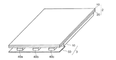
図1は、本発明の第1の実施形態に係る液晶表示装置の部分的な構造を説明するための斜視図である。この液晶表示装置は、透過型(または半透過型)の液晶表示装置であって従来とほぼ同様の構成を有するが、従来の構成とは異なって映像信号伝送用のFPC基板を備えず、新たに信号伝送用の後述する受光素子および受信回路を備える。<1. First Embodiment>
<1.1 Overall configuration and operation>
FIG. 1 is a perspective view for explaining a partial structure of a liquid crystal display device according to a first embodiment of the present invention. This liquid crystal display device is a transmissive (or transflective) liquid crystal display device and has almost the same configuration as the conventional one. However, unlike the conventional configuration, the liquid crystal display device does not include an FPC board for video signal transmission, and is newly added. Includes a light receiving element and a receiving circuit, which will be described later, for signal transmission.
図1に示されるように、この液晶表示装置は、従来と同様のCF基板10および受光素子および受信回路が形成された従来とは異なるTFT基板20を含む液晶パネル(液晶表示ユニット)2と、透過表示のためのバックライト光源となる白色LED40a〜40cおよび導光板等の光学部材30を含むバックライト部(バックライトユニット)3とを備える。また、このバックライト部3に含まれる白色LED40a〜40cには、装置外部の信号源からFPC基板(およびLED駆動回路)を介して所定の変調方式により変調された信号(被変調信号)を含む電流が与えられる。なお、LEDは高輝度で低消費電力の発光素子であるとともに、高速に点灯および非点灯を繰り返すことができるので、本実施形態の発光素子として好適である。詳しくは後述する。
As shown in FIG. 1, this liquid crystal display device includes a liquid crystal panel (liquid crystal display unit) 2 including a
なお従来の構成と同様、液晶パネル2の少なくとも片面には偏光シートが貼付されており、バックライト部3に含まれる導光体である導光板における光の出射面にはレンズシートや光拡散シート等が貼付され、その反対側の面には反射シートが貼付されている。この構成により、バックライト部3は、液晶表示のためのバックライト照明を与える面状照明装置として機能する。また、ここでは白色LED40a〜40cは3個設けられているが、その数に特に限定はない。
As in the conventional configuration, a polarizing sheet is attached to at least one surface of the
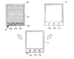
図2は、バックライト部3の構成を簡略に説明するための平面図である。図2の上段左側に示される下ベゼル部60は、トレイ状の形状であって、導光板等の光学部材30と、白色LED40a〜40cを搭載したFPC基板50とを所定の位置関係に固定されるよう格納している。なお、FPC基板50の一端には、白色LED40a〜40cを駆動するための電流を受け取るFPC入力端子59が形成されている。
FIG. 2 is a plan view for simply explaining the configuration of the
この下ベゼル部60の上側すなわち液晶パネル2に対向する光出射面側に、図2の上段右側に示される貫通孔71a〜71cを有する樹脂シャーシ70を被せるように固定することによって、図2の下段に示されるバックライト部3が作製される。
By fixing the
ここで、この図2の下段に示されるように、樹脂シャーシ70における貫通孔71a〜71cの位置は、バックライト部3の白色LED40a〜40cの位置と一意に対応している。したがって、白色LED40a〜40cから出射される光は、導光板等を経てその出射面から上側(液晶パネル2側)へ出射されるとともに、対応する貫通孔71a〜71cを通って液晶パネル2の後述する受光素子へ与えられる。
Here, as shown in the lower part of FIG. 2, the positions of the through
以上のように作製されるバックライト部3は、液晶パネル2の下部すなわち表示面とは反対側に配置される。図3は、これらバックライト部および液晶パネルを含む液晶モジュールの構成を簡略に説明する図である。図3に示されるように、バックライト部3は液晶パネル2の下部に配置され、この液晶パネル2の上側(表示面側)から上ベゼル80を被せるように固定することによって、図3の下段に示される液晶モジュール4が作製される。
The
なお、液晶パネル2(におけるCF基板10)の表示面側には遮光性のブラックマトリクス11が形成されている。このブラックマトリクス11は、バックライト部3からの光が表示面以外から漏れ出すのを防ぐとともに、TFT基板20に形成される回路が外光の影響を受けないようにする。このブラックマトリクス11の構造は周知であるため詳しい説明は省略する。
A light-shielding
図4は、受光素子と白色LEDとの位置関係を説明するための図である。図4の上段左側に示されるように、液晶パネル2の裏面すなわち表示面とは反対側の面には、所定の間隔をあけて受光素子90a〜90cが形成されている。具体的には、この受光素子90a〜90cは、TFT基板20のガラス基板上にTFTの製造プロセスと同様の製造プロセスにより形成されるPIN型光ダイオードであり、白色LED40a〜40cからの光を受け取ることによりその強度に応じた量の電流を出力する。この構造については後述する。なお、図3において前述したように、この液晶パネル2の表面すなわち表示面側にブラックマトリクス11が形成されている。
FIG. 4 is a diagram for explaining the positional relationship between the light receiving element and the white LED. As shown in the upper left side of FIG. 4,
図4に示されるように、上記液晶パネル2の裏面に形成される受光素子90a〜90cは、それぞれバックライト部3に配置される白色LED40a〜40cと一意に対応する位置に固定される。例えば、白色LED40cから出射される光は、貫通孔71cを通して受光素子90cに与えられる。なお、白色LED40a〜40cから導光板へ向かう光は拡散され混合されるが、白色LED40a〜40cから受光素子90a〜90cに与えられる光はそれぞれ混合されてはならない(少なくとも好ましくない)ので、白色LED40a〜40cからの光がそれぞれ一意に対応する貫通孔71a〜71cの1つのみを通過するよう白色LED40a〜40cの間を遮光する隔壁または導光部等が設けられてもよい。また、外光等の不要光が受光素子90a〜90cに入射しないよう遮光する隔壁または囲いが貫通孔71a〜71c周囲に設けられてもよい。さらに、貫通孔71a〜71c内にガラス等を充填してもよいし、複数の異なる屈折率を有する素材を光ファイバの断面構造に類似する構造となるよう配置した導光部が設けられてもよい。次に、受光素子90a〜90c(以下、これらを区別しない場合に「受光素子90」という)について、図5および図6を参照して説明する。
As shown in FIG. 4, the
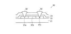
<1.2 受光素子の構成および特性>
図5は、受光素子90の構造を簡略に示す断面図である。図5に示されるように、この受光素子90は、TFT基板20に含まれるガラス基板21上に形成された半導体層91と、この半導体層91を覆うように形成されたゲート絶縁膜22と、その上層に形成された層間絶縁膜23と、これらの絶縁膜を貫通するように開口されたコンタクトホールを介して半導体層91の一部に電気的に接続される電極92とを備える。なお、平坦化膜等の記載は省略した。<1.2 Configuration and characteristics of light receiving element>
FIG. 5 is a cross-sectional view schematically showing the structure of the
また、半導体層91におけるP領域91aおよびN領域91cには所定の不純物がドープされ、i領域91bには不純物がドープされないため、図5に示されるようにガラス基板21の面に沿った方向にPIN接合が形成されている。このような構造の受光素子90は、周知であって、横型(ラテラル型)構造のPIN型光ダイオードと呼ばれる。このような構造を有する受光素子90は、TFTと同一のプロセスにより形成することができるので、安価に作製することができる。なお、上記半導体層に使用されるシリコンは、非結晶シリコンであってもよいが、回路の集積度を向上させるためには多結晶シリコンであることが好ましく、さらには電子移動度の高い連続粒界(CG:Continuous Grain)シリコンであることがより好ましい。なお、このようにTFT基板20上に一体的に形成される受光素子90に代えて、個別の受光素子(例えば一般的な光ダイオード素子)をTFT基板20上に実装する構成であってもよい。
In addition, since the
また、この受光素子90の構造は、可視光(ここでは白色光)を使用する本発明における光伝送方式に適している。図6は、この受光素子90に対して異なる波長の光を照射した場合に測定された電流値を示す図である。なお、測定に使用した受光素子90のゲート長Lは7[μm]であり、ゲート幅は5000[μm]である。
Further, the structure of the
図6に示されるように、この受光素子90は、光の波長が長くなるに従って出力電流が小さくなる(すなわち感度が小さくなる)が、白色光についての感度は比較的高いといえる。これに対して、一般的な(薄膜でない)光ダイオード素子は、主として赤外線領域において出力電流が大きくなることが多いので、白色光についての感度は低いことが多い。したがって、この受光素子90は、白色光を使用する本発明における光伝送方式に好適である。次に、本実施形態における液晶表示装置の回路構成について説明する。
As shown in FIG. 6, the
<1.3 表示装置の全体的な回路構成>
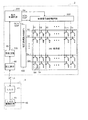
図7は、本発明における第1の実施形態に係る液晶表示装置の回路構成を示すブロック図である。この液晶表示装置は、液晶パネル2のTFT基板20上に形成される受光素子90、受信回路100、表示制御回路200、映像信号線駆動回路300、走査信号線駆動回路400、および表示部500と、バックライト部3に含まれる白色LED40a〜40c(以下、これらを区別しない場合に「白色LED40」という)およびLED駆動回路51とを備えている。<1.3 Overall circuit configuration of display device>
FIG. 7 is a block diagram showing a circuit configuration of the liquid crystal display device according to the first embodiment of the present invention. The liquid crystal display device includes a
この液晶表示装置に表示されるべき画像を表す信号および所定のタイミング信号等を含む映像信号VSは、装置外部からFPC基板50の入力端子59から、FPC基板50の内部に形成されまたは集積回路としてFPC基板50上に実装されるLED駆動回路51に与えられる。このLED駆動回路51は、映像信号VSに応じた光(変調)信号LSを出力(発光)する白色LED40を駆動する。このLED駆動回路51の詳細な構成は後述する。なお、LED駆動回路51は、必ずしもFPC基板50上に実装される必要はない。また、受信回路100およびその他の回路は、必ずしもTFT基板20上に一体的に形成される必要はなく、集積回路としてTFT基板20上に実装されるなど、どのような形態であってもよい。
A video signal VS including a signal representing an image to be displayed on the liquid crystal display device and a predetermined timing signal is formed from the
TFT基板20に含まれる受光素子90は、バックライト部3に含まれる白色LED40から受け取った光信号LSを電気信号に変換して受信回路100に与える。受信回路100は、受け取った電気信号から映像信号VSを生成(復調)して表示制御回路200に与える。
The
表示制御回路200は、受信回路100から受け取った映像信号VSに基づき、液晶パネルにおける表示のため映像信号線駆動回路300に与えられるソース用クロック信号SCKおよびソース用スタートパルス信号SSPと、表示のため走査信号線駆動回路400に与えられるゲート用クロック信号GCKおよびゲート用スタートパルス信号GSPとを含む各種信号を生成する。なお、これらの信号は周知であるため詳しい説明は省略する。また、表示制御回路200は、映像信号VSに基づきデジタル画像信号Daを映像信号線駆動回路300に供給する。
The
映像信号線駆動回路300には、上記のように、表示部500に表示すべき画像を表すデータが画素単位でデジタル画像信号Daとして供給されると共に、タイミングを示す信号としてソース用クロック信号SCKおよびソース用スタートパルス信号SSPなどが供給される。映像信号線駆動回路300は、これらのデジタル画像信号Da、ソース用クロック信号SCK、およびソース用スタートパルス信号SSPなどに基づき、表示部500を駆動するためのアナログ電圧である駆動用映像信号S1,S2,S3,…,Sn(nは映像信号線数)を生成し、これを表示部500の各映像信号線に印加する。この駆動用映像信号S1,S2,S3,…,Snは、表示部500の交流化駆動のために、図示されない極性切換制御信号に応じてその極性が反転する。
As described above, the video signal
走査信号線駆動回路400は、ゲート用クロック信号GCKおよびゲート用スタートパルス信号GSPに基づき、表示部500における走査信号線を1水平走査期間ずつ順に選択するために各走査信号線に印加すべき走査信号G1,G2,G3,…,Gm(mは走査信号線数)を生成し、全走査信号線のそれぞれを順に選択するためのアクティブな走査信号の各走査信号線への印加を1垂直走査期間を周期として繰り返す。
Based on the gate clock signal GCK and the gate start pulse signal GSP, the scanning signal
表示部500は、映像信号により表される画像における水平走査線にそれぞれが対応する複数本の走査信号線(行電極)と、それら複数本の走査信号線のそれぞれと交差する複数本の映像信号線(列電極)と、それら複数本の走査信号線と複数本の映像信号線との交差点にそれぞれ対応して設けられた複数の画素形成部とを含む。 The display unit 500 includes a plurality of scanning signal lines (row electrodes) each corresponding to a horizontal scanning line in an image represented by a video signal, and a plurality of video signals intersecting each of the plurality of scanning signal lines. A line (column electrode) and a plurality of pixel formation portions provided corresponding to the intersections of the plurality of scanning signal lines and the plurality of video signal lines.
上記各画素形成部は、対応する交差点を通過する映像信号線にソース端子が接続されるとともに、対応する交差点を通過する走査信号線にゲート端子が接続されたTFT501と、そのTFT501のドレイン端子に接続された画素電極と、上記複数の画素形成部に共通的に設けられた共通電極(「対向電極」ともいう)Ecと、上記複数の画素形成部に共通的に設けられ画素電極と共通電極Ecとの間に挟持された液晶層とからなる。そして、画素電極Epと共通電極Ecとそれらの間に挟持された液晶層とにより画素容量Cpが形成される。なお、TFT基板20は、上記信号線、TFT、および画素電極等を含んでおり、CF基板10は、上記共通電極Ecおよび図示されないカラーフィルタや各種光学補償フィルムなどを含んでいる。
Each pixel forming portion has a
上記構成からわかるように、表示部500では、いずれかの走査信号線Lgに印加される走査信号Gk(kは1〜mの自然数)がアクティブになると、その走査信号線が選択されて、その走査信号線に接続される各画素形成部のTFT501が導通状態となり、そのTFT501に接続される画素電極には、駆動用映像信号Sj(jは1〜nの自然数)が映像信号線を介して印加される。これにより、その印加された駆動用映像信号Sjの電圧(共通電極Ecの電位を基準とする電圧)が、その画素電極を含む画素形成部に画素値として書き込まれる。これにより表示部500は、映像信号VSの表す画像を表示する。次に、図8を参照してLED駆動回路51の詳細な回路構成について説明する。
As can be seen from the above configuration, in the display unit 500, when the scanning signal Gk (k is a natural number of 1 to m) applied to any of the scanning signal lines Lg becomes active, the scanning signal line is selected, The
<1.4 LED駆動回路の構成>
図8は、LED駆動回路51の詳細な構成を示すブロック図である。図8に示されるように、このLED駆動回路51は、本液晶表示装置の外部から映像信号VSとLED駆動回路51の電源等の動作を制御するパワーコントロール信号PSとを受け取ってこれらを多重化するマルチプレクサ511と、多重化された信号を周知のマルチリンク方式により3つの信号に分離する分離部512と、分離部512から受け取った対応する信号に基づき所定の信号を変調した変調信号に基づき白色LED40a〜40cを駆動するための被変調信号を含む駆動電流を出力する変調部515a〜515cと、白色LED40a〜40cを駆動するための電流を変調部515a〜515cに与える電流源514と、変調部515a〜515cによる白色LED40a〜40cの駆動電流に基づき電流源514の出力電流を調整する調整部516と、パワーコントロール信号PSに基づき電流源514の動作を停止させまたは開始させる制御を行うバックライト電源制御部513とを備える。<1.4 LED drive circuit configuration>
FIG. 8 is a block diagram showing a detailed configuration of the
なお、上記映像信号VSおよびパワーコントロール信号PSは、前述したように装置外部からFPC基板50の入力端子59を介してマルチプレクサ511に与えられるが、FPC基板50の入力端子59とは異なる入力端子から与えられてもよいし、FPC基板50を介することなく与えられてもよい。
The video signal VS and the power control signal PS are supplied from the outside of the apparatus to the
マルチプレクサ511は、受け取った映像信号VSおよびパワーコントロール信号PSを多重化するが、これらの信号はデジタル信号であるので、これらを周知のデジタル多重化方式により多重化した信号もまたデジタル信号である。なお、このパワーコントロール信号PSは後述するように光信号に変換されてTFT基板20に含まれる受信回路100に送信されるが、TFT基板20に対する電源制御が不要である場合には送信されない構成であってもよい。この場合には、マルチプレクサ511は省略される。
The
このパワーコントロール信号PSは、上記マルチプレクサ511の他、バックライト電源制御部513にも与えられる。このパワーコントロール信号PSは、装置外部からの制御信号であって、装置が動作中はアクティブであり、装置が停止される場合には非アクティブとなる。バックライト電源制御部513は、このパワーコントロール信号PSが非アクティブとなったときに電流源514の動作を停止させ、アクティブとなったときに電流源514の動作を開始させる制御を行う。なお、このバックライト電源制御部513は、LED駆動回路51に含まれる電流源514以外の回路を同時に停止または開始させる制御を行うのが好ましい。なお、このパワーコントロール信号PSは、光信号に変換されて送信されるので、バックライト電源制御部513はこの送信動作が終了後に上記停止動作を行うのが好ましい。
This power control signal PS is given not only to the
分離部512は、白色LED40a〜40cと受光素子90a〜90cとの間に形成される3つの光伝送経路に対して、伝送されるべき情報としてのマルチプレクサ511により多重化されたデジタル信号が分かれて伝送されるよう、当該多重化された信号を3つに分離する。このように、複数の物理的な伝送経路に対して伝送すべき情報を分けて伝送することをマルチリンクという。このマルチリンクを行うために信号を分離する分離部512は、具体的には、上記多重化されたデジタル信号を例えば時系列に沿って所定量毎に3つに分割して1/3の分周比で分周することにより周波数を下げて(例えばパルス周期を長くして)変調部515a〜515cに与える。この構成により、白色LED40a〜40cを駆動可能な最大周波数が映像信号VSまたはこれに基づき変調された信号の周波数を下回る場合(例えば約半分である場合)にも、このようなマルチリンク方式により白色LED40a〜40cを駆動することができる。
The
変調部515a〜515cは、分離部512から受け取った信号に基づき、図示されない局部発信器から得られる所定の周波数の搬送波を例えばデジタル変調する。なお、上記周波数は、少なくとも目に見えないまたは目に感じにくい周波数が好ましい。このようなデジタル変調方式にはASK(Amplitude Shift Keying)、FSK(Frequency Shift Keying)、PSK(Phase Shift Keying)などの各種帯域伝送方式があり、またRZ(Return to Zero)方式などの各種ベースバンド伝送方式があり、ここではいずれも採用可能である。なお本明細書では、変調部515a〜515cにおける変調は、帯域伝送方式における変調の他、上記ベースバンド伝送方式における信号の変換や符号化などを広く含むものとする。さらに、これらを使用したCDMA(Code Division Multiple Access)などの周知の各種多元接続方式を採用することも可能である。
Based on the signal received from the
なお、変調部515a〜515cは省略され、分離部512からの分離された3つの信号それぞれをそのまま、または増幅器を介して白色LED40a〜40cに与える構成であってもよい。また、周知の各種アナログ変調方式が採用されてもよい。次に、図9および図10を参照して、これらの変調方式のいくつかについて説明する。
The
図9は、帯域伝送方式のデジタル変調方式による変調を受けた被変調信号を簡略に示す波形図である。なお、各信号の下に付された数字は、変調信号であるデジタル信号の情報内容を示している。 FIG. 9 is a waveform diagram schematically showing a modulated signal that has been modulated by the digital modulation method of the band transmission method. In addition, the number attached | subjected under each signal has shown the information content of the digital signal which is a modulation signal.
図9の上段部に示される波形図は、2値ASK方式の被変調信号を示している。この2値ASKとは、デジタル信号における1ビットの情報(「1」または「0」)を搬送波における2種類の振幅(または搬送波の有無)に対応させる変調方式である。図9の下段部に示される波形図は、4値ASK方式の被変調信号を示している。この4値ASKとは、デジタル信号における2ビットの情報を搬送波における4種類の振幅に対応させる変調方式である。なお、これらの帯域伝送方式は、受信側における被変調信号の分離が容易であり、伝送誤りを少なくすることができる。 The waveform diagram shown in the upper part of FIG. 9 shows a binary ASK modulated signal. The binary ASK is a modulation method in which 1-bit information (“1” or “0”) in a digital signal is associated with two types of amplitudes (or presence / absence of a carrier wave). The waveform diagram shown in the lower part of FIG. 9 shows a 4-level ASK modulated signal. The four-value ASK is a modulation method that associates 2-bit information in a digital signal with four types of amplitudes in a carrier wave. Note that these band transmission systems can easily separate modulated signals on the receiving side, and can reduce transmission errors.
図10は、ベースバンド伝送方式のデジタル変調方式による変調を受けた被変調信号を簡略に示す波形図である。なお、各信号の下に付された数字は、変調信号であるデジタル信号の情報内容を示している。なお、これらのベースバンド方式によりパルス列からなるデジタル信号を伝送する場合にはフリッカを生じにくくすることができる。 FIG. 10 is a waveform diagram schematically showing a modulated signal that has been modulated by the digital modulation scheme of the baseband transmission scheme. In addition, the number attached | subjected under each signal has shown the information content of the digital signal which is a modulation signal. Note that flicker is less likely to occur when a digital signal composed of a pulse train is transmitted by these baseband methods.
図10の上段部に示される波形図は、RZ方式の被変調信号を示している。このRZとは、符号の送出間隔よりパルス幅が短く、そのため一旦0電位に戻る伝送方式である。図10の中段部に示される波形図は、PPM(Pulse Position Modulation)方式の被変調信号を示している。このPPMとは、デジタル信号における(図では2ビットの)情報を搬送波における(ここでは4種類の)パルスの位置に対応させる変調方式である。図10の下段部に示される波形図は、CDMA方式の被変調信号を示している。このCDMAとは、デジタル信号における(図では1ビットの)情報を固有のパルス系列を有する符号に対応させる変調方式である。なお、図9および図10に示される波形図は説明のために簡略化されており、変調部515a〜515cから出力される実際の信号の波形とは異なる。
The waveform diagram shown in the upper part of FIG. 10 shows a modulated signal of the RZ system. This RZ is a transmission method in which the pulse width is shorter than the transmission interval of the code and, therefore, temporarily returns to 0 potential. The waveform diagram shown in the middle part of FIG. 10 shows a PPM (Pulse Position Modulation) type modulated signal. This PPM is a modulation method that associates information (2 bits in the figure) in a digital signal with the positions of pulses (here, four types) in a carrier wave. The waveform diagram shown in the lower part of FIG. 10 shows a CDMA modulated signal. The CDMA is a modulation method in which information (1 bit in the figure) in a digital signal is associated with a code having a unique pulse sequence. The waveform diagrams shown in FIGS. 9 and 10 are simplified for the sake of explanation, and are different from the waveforms of actual signals output from the
ここで、上記CDMA方式では、上記固有の符号以外の符号をノイズとみなせるので、受信側では固有の符号に基づき所望の被変調信号のみを他の被変調信号等から分離可能であることが知られている。よって、本実施形態においてCDMA方式の光信号が使用される場合、白色LED40a〜40cからの光がそれぞれ一意に対応する受光素子90a〜90cにのみ入射されるように工夫された構成(例えば貫通孔71a〜71cなど)は特に必要ではなく、例えば導光板からの光を受け取る構成であってもよい。さらには、受光素子が1つだけ備えられる構成であってもよい。このような場合であっても簡易な構成で多元接続を実現することができる。
Here, in the CDMA system, since codes other than the unique code can be regarded as noise, it is known that only the desired modulated signal can be separated from other modulated signals based on the unique code on the receiving side. It has been. Therefore, when a CDMA optical signal is used in the present embodiment, a configuration devised so that light from the
変調部515a〜515cは、電流源514から受け取った電流に基づき、以上のような変調方式による変調を受けた被変調信号を駆動電流として白色LED40a〜40cを駆動する。白色LED40a〜40cは、受け取った被変調信号に応じて例えば強度変調された光信号LSを出力する。また、調整部516は、変調部515a〜515cによる白色LED40a〜40cの駆動電流や温度等を監視しており、監視結果に基づき所定の値からのずれが生じている場合には電流源514の出力電流を所望の値となるよう調整する。次に、図11を参照して受信回路100の詳細な構成を説明する。
Based on the current received from the
<1.5 受信回路の構成>
図11は、受信回路100の詳細な構成を示すブロック図である。図11に示されるように、この受信回路100は、受光素子90a〜90cにより光信号LSから変換された電気信号を受け取る図示されない駆動回路と、対応する駆動回路から出力される電気信号を復調する復調部101a〜101cと、これら復調部101a〜101cからの分離された信号を復元する復元部103と、この復元部103からの信号を受け取り映像信号VSおよびパワーコントロール信号PSを取り出すデマルチプレクサ104と、このデマルチプレクサ104から出力されるパワーコントロール信号PSを受け取る受信側電源制御部105とを備える。また、デマルチプレクサ104から出力される映像信号VSは、表示制御回路200に与えられる。
<1.5 Receiver circuit configuration>
FIG. 11 is a block diagram showing a detailed configuration of the receiving
この受信回路100に含まれる復調部101a〜101cは、変調部515a〜515cにおいて採用された変調方式に対応した復調方式を採用し、復元部103は分離部512において採用されたマルチリンク方式に対応した復元方式を採用し、デマルチプレクサ104はマルチプレクサ511において採用された多重化方式に対応した復調方式を採用する。これらの方式は周知であるため説明を省略する。
受信側電源制御部105は、デマルチプレクサ104から受け取ったパワーコントロール信号PSが非アクティブとなったときに受信回路100に含まれる各回路の動作を停止させる制御を行う。なお、これらの回路の動作開始は、受信側電源制御部105により図示されない制御信号を受け取ったときになされるものとする。
The reception-side power
ここで、この受信回路100は、受光素子90a〜90cのうちの1つ以上から出力される電流を監視するキャリア検知部をさらに備えていてもよい。このキャリア検知部は、受信回路100に含まれる各回路の動作停止中も継続的に上記電流の有無を監視することにより、光信号を検知する。そして、キャリア検知部は光信号を検知した場合、受信側電源制御部105に所定の検知信号を送り、受信側電源制御部105はこの検知信号を受け取った場合に受信回路100に含まれる各回路の動作を開始させる制御を行う。なお、キャリア検知部の検知対象であるキャリアは例示であって正確には光そのものを指し、キャリアとして機能しない光を検知する場合も含まれる。
Here, the receiving
また、このキャリア検知部が備えられる場合、マルチプレクサ511およびデマルチプレクサ104が省略される構成、すなわちパワーコントロール信号PSによる電源制御を行わない構成であってもよい。この構成において、キャリア検知部は光信号を検知した場合、受信側電源制御部105にアクティブである検知信号を送り、受信側電源制御部105はこのアクティブである検知信号を受け取った場合に受信回路100に含まれる各回路の動作を開始させる(また動作中は動作状態を維持する)制御を行う。また、キャリア検知部は光信号を検知しない場合(より好ましくは光信号を検知しなくなってから所定の期間が経過した場合)、受信側電源制御部105に所定の非アクティブである検知信号を送り、受信側電源制御部105はこの非アクティブである検知信号を受け取った場合に受信回路100に含まれる各回路の動作を停止させる(また停止中は停止状態を維持する)制御を行う。
When this carrier detection unit is provided, a configuration in which the
なお、これらの場合において受信側電源制御部105は、TFT基板2に含まれる表示制御回路200などの各回路の動作を上記と同様に停止させまたは開始させる制御を行ってもよい。そうすれば、白色LED40a〜40cの動作が停止しまたは開始した場合には自動的にTFT基板2に含まれる各回路の動作が停止しまたは開始するので、TFT基板2に含まれる各回路の電源制御を簡易な構成で行うことができる。
In these cases, the receiving-side
<2. 第2の実施形態>
次に、上記第1の実施形態の場合とは異なり、本実施形態では、白色LED40a〜40cが動作中すなわちバックライト照明が行われている期間中、白色LED40a〜40cが非常に短い時間間隔、例えば100[KHz]程度の視認できない周波数で点灯と消灯とを繰り返し行う、いわゆる調光制御が行われる。この調光制御は、点灯時間と消灯時間との割合を示すデューティ比を変更することにより行われ、例えば消灯時間の割合が増加するほど全体として白色LED40a〜40cの明るさが暗くなる。このことにより、例えば外光の明るさに応じた好適な所望の明るさを有するバックライト照明を提供することができるとともに、白色LED40a〜40cを常時点灯させる場合に比べて消費電力を低減することができる。このような調光制御が行われる場合の液晶表示装置の回路構成について説明する。<2. Second Embodiment>
Next, unlike the case of the first embodiment, in this embodiment, the
ここで、本実施形態における液晶表示装置の構造およびその全体的な回路構成は、第1の実施形態の場合と同様であるので、同一の構成要素には同一の符号を付してその説明を省略する。本液晶表示装置は、第1の実施形態の場合とは異なりパワーコントロール信号PSを受け取らず、これに代えて装置外部から調光制御のための調光パラメータ信号LCを受け取る点が異なっている。そこでまず、本実施形態におけるLED駆動回路の詳細な構成について説明する。 Here, since the structure of the liquid crystal display device and the overall circuit configuration thereof in this embodiment are the same as those in the first embodiment, the same components are denoted by the same reference numerals and the description thereof is omitted. Omitted. Unlike the case of the first embodiment, the present liquid crystal display device is different in that it does not receive the power control signal PS and instead receives a dimming parameter signal LC for dimming control from the outside of the device. First, the detailed configuration of the LED drive circuit in this embodiment will be described.
<2.1 LED駆動回路の構成>
図12は、本発明における第2の実施形態におけるLED駆動回路52の詳細な構成を示すブロック図である。図12に示されるように、このLED駆動回路52は、第1の実施形態において受け取るパワーコントロール信号PSに代えて、本液晶表示装置の外部から調光制御のための調光パラメータ信号LCを受け取る。<2.1 Configuration of LED drive circuit>
FIG. 12 is a block diagram showing a detailed configuration of the LED drive circuit 52 according to the second embodiment of the present invention. As shown in FIG. 12, the LED drive circuit 52 receives a dimming parameter signal LC for dimming control from the outside of the present liquid crystal display device instead of the power control signal PS received in the first embodiment. .
よって、本実施形態におけるマルチプレクサ511は、映像信号VSと調光パラメータ信号LCとを受け取ってこれらを多重化する。なお、これらの信号は、前述したように装置外部からFPC基板50の入力端子59を介してマルチプレクサ511に与えられる。この調光パラメータ信号LCは、調光制御のためのパラメータであり、具体的にはデューティ比を示す数値である。
Therefore, the
また、図12に示されるように、このLED駆動回路52は、第1の実施形態において備えられるバックライト電源制御部513に代えて、調光パラメータ信号LCを受け取る調光制御部517を備える。この調光制御部517は、調光パラメータ信号LCに含まれるデューティ比を有する所定のPWM(Pulse Width Modulation)方式の変調を受けた光信号LSを白色LED40a〜40cに出力させるため、電流源514から変調部515a〜515cに対して与えられる電流量を変化させる。なお、このように白色LED40a〜40cがPWMなどを利用したパルスによる調光制御を受けている場合には、当該パルスを使用してベースバンド伝送を行うことが可能となるため、ダイナミックレンジを広く取ることができ、効率のよい光伝送が可能となる。
As shown in FIG. 12, the LED drive circuit 52 includes a
図13は、このような調光制御を受けた光信号LSの簡略な波形図であり、より詳しくは図13の上段に示される波形図は、光信号LSの全体的な強度変化を説明するための図であり、図13の下段に示される波形図は、光信号LSの一部の強度変化を説明するための拡大図である。ここで、図13に示される信号波形のオン期間(点灯期間)において、送出される光信号LSは変調部515a〜515cによる変調を受けているが、オフ期間(消灯期間)においては光信号LSが送出されないので、当然に変調部515a〜515cによる変調を受けていない。したがって、本実施形態におけるLED駆動回路52は、この間に光信号LSにより映像信号VSを伝送することができない。そこで、調光制御部517は、分離部512(またはマルチプレクサ511)を制御することにより、この間の信号送出を停止させる。なお、この場合、分離部512(またはマルチプレクサ511)には所定のFIFOメモリが内蔵されており、信号送出が停止されている間に受け取ったデータは一時的にこのメモリに格納されるものとする。次に、以上のような調光制御を受けた光信号LSを受信する受信回路120の詳細な構成について説明する。
FIG. 13 is a simplified waveform diagram of the optical signal LS that has undergone such dimming control. More specifically, the waveform diagram shown in the upper part of FIG. 13 explains the overall intensity change of the optical signal LS. The waveform diagram shown in the lower part of FIG. 13 is an enlarged view for explaining a partial intensity change of the optical signal LS. Here, in the ON period (lighting period) of the signal waveform shown in FIG. 13, the transmitted optical signal LS is modulated by the
<2.2 受信回路の構成>
図14は、第2の実施形態における受信回路120の詳細な構成を示すブロック図である。図14に示されるように、この受信回路120は、第1の実施形態において受信側電源制御部105に代えて、受け取った調光パラメータ信号LCを解析する調光信号解析部106を備える。<2.2 Configuration of receiving circuit>
FIG. 14 is a block diagram illustrating a detailed configuration of the receiving circuit 120 according to the second embodiment. As shown in FIG. 14, the reception circuit 120 includes a dimming signal analysis unit 106 that analyzes the received dimming parameter signal LC instead of the reception-side power
この調光信号解析部106は、デマルチプレクサ104により復調された調光パラメータ信号LCを受け取り、当該調光パラメータ信号LCに含まれるデューティ比に応じた好適な受光感度および増幅率を解析する。例えば、調光信号解析部106は、各デューティ比に好適な受光感度および増幅率の対応関係を示すテーブルを記憶しており、この対応テーブルに基づき上記受光感度および増幅率を算出する。調光信号解析部106は、この算出された受光感度および増幅率になるよう駆動回路101a〜101cの受光感度および増幅率を調整する制御を行う。
The dimming signal analysis unit 106 receives the dimming parameter signal LC demodulated by the
また、調光信号解析部106は、調光パラメータ信号LCに含まれるデューティ比を参照して、図13の下段に示されるようなオン期間とオフ期間との開始時点(および終了時点)を推測し、復調部101a〜101cおよび復元部103に上記開始時点を示す信号を与える。例えば、調光信号解析部106は、例えばデマルチプレクサ104から映像信号VSを受け取ることにより同期クロックを生成する周知の位相同期回路(PLL:Phase Locked Loop)回路からなるクロック再生回路を内蔵しており、このクロックを計数することにより映像信号VSが出力されない場合であってもオン期間とオフ期間との開始時点を推測することができる。
In addition, the dimming signal analysis unit 106 estimates the start time (and end time) of the on period and the off period as shown in the lower part of FIG. 13 with reference to the duty ratio included in the dimming parameter signal LC. and provides a signal indicating the start time to the
復調部101a〜101cは、調光信号解析部106からオン期間が開始されることを示す信号を受け取るときに駆動回路から出力される電気信号を復調し、オフ期間が開始されることを示す信号を受け取るときに駆動回路から出力される電気信号の復調を停止する。また、同様に、復元部103は調光信号解析部106からオン期間が開始されることを示す信号を受け取るときに復調部101a〜101cからの分離された信号を復元し、オフ期間が開始されることを示す信号を受け取るときに復元動作を停止する。このことにより、オフ期間においても上記復調動作および復元動作が継続されることにより誤った映像信号VSが生成されることを防止することができる。なお、復元部103は、復元された映像信号VSを含む信号を一旦蓄積するためのバッファメモリを備え、オン期間中のみならずオフ期間中も連続的に映像信号VSを生成する構成が好ましい。
ここで、この受信回路120は、調光信号解析部106に代えて、受光素子90a〜90cのうちの1つ以上から出力される電流を監視するキャリア検知部を備えていてもよい。このキャリア検知部が備えられる場合、マルチプレクサ511およびデマルチプレクサ104が省略される構成、すなわち調光パラメータ信号LCが受信回路120に与えられない構成となる。この構成において、キャリア検知部は光信号を検知した場合、復調部101a〜101cおよび復元部103にアクティブである検知信号を送り、光信号を検知しない場合、復調部101a〜101cおよび復元部103に非アクティブである検知信号を送る。また、キャリア検知部は、上記アクティブ期間および非アクティブ期間の長さを記憶しておき、記憶されたこれらの割合に基づき調光制御におけるデューティ比を算出し、このデューティ比に応じた好適な受光感度および増幅率を解析する。キャリア検知部は、この算出された受光感度および増幅率になるよう駆動回路の受光感度および増幅率を調整する制御を行うことができる。
Here, the receiving circuit 120 may include a carrier detection unit that monitors a current output from one or more of the
なお、このキャリア検知部は、PLL回路からなる周知のクロック再生回路を内蔵しており、この回路に基づき光信号を検知する期間と光信号を検知しない期間とを推測して、適宜上記アクティブである検知信号または非アクティブである検知信号を生成する構成であってもよい。 The carrier detection unit incorporates a well-known clock recovery circuit composed of a PLL circuit. Based on this circuit, the carrier detection unit estimates a period during which an optical signal is detected and a period during which no optical signal is detected. It may be configured to generate a certain detection signal or an inactive detection signal.
復調部101a〜101cおよび復元部103は、この検知信号がアクティブであるときには復調および復元動作を行い、非アクティブであるときには復調および復元動作を行わない。このことにより、オフ期間においても上記復調動作および復元動作が継続されることにより誤った映像信号VSが生成されることを防止することができる。
なお、この場合において変調部515a〜515cの変調方式として調歩同期方式が採用されるときには、情報がない場合にもストップビットを含む光信号が送出されるので、復調回路102a〜102cおよび復元部103は、キャリア検知部により光信号に含まれる情報の始まりを示すスタートビットが検知される場合に復調および復元動作を開始し、かつキャリア検知部によりストップビットが検知される場合には復調および復元動作を継続する。このことから信号解析部106によりオン期間とオフ期間との開始時点を推測する必要がない。
In this case, when the start-stop synchronization method is adopted as the modulation method of the
また、この場合において新たに電源制御部が設けられ、電源制御部により上記検知信号が所定期間継続して非アクティブである場合にはTFT基板2に含まれる表示制御回路200などの各回路の動作を停止させ、その後検知信号がアクティブとなったときに各回路の動作を開始させる制御が行われてもよい。そうすれば、白色LED40a〜40cの動作が停止しまたは開始した場合には自動的にTFT基板2に含まれる各回路の動作が停止しまたは開始するので、TFT基板2に含まれる各回路の電源制御を簡易な構成で行うことができる。
Further, in this case, when a power supply control unit is newly provided and the detection signal is inactive for a predetermined period by the power supply control unit, the operation of each circuit such as the
さらに、本実施形態における液晶表示装置は、パワーコントロール信号PSを受け取らない構成であるが、調光パラメータ信号LCを受け取るとともに、併せて第1の実施形態の場合と同様にパワーコントロール信号PSを受け取る構成であってもよい。すなわち、本実施形態における液晶表示装置は、第1の実施形態における液晶表示装置の回路を含むこともできる。 Further, the liquid crystal display device in the present embodiment is configured not to receive the power control signal PS, but receives the dimming parameter signal LC and also receives the power control signal PS as in the case of the first embodiment. It may be a configuration. That is, the liquid crystal display device in the present embodiment can also include the circuit of the liquid crystal display device in the first embodiment.
<3. 第3の実施形態>
次に、上記第1および第2の実施形態の場合とは異なり、本実施形態における液晶表示装置は、映像を表示する主たる機能の他、音声を再生する機能が付加されている。すなわち本実施形態では、映像信号VSが従来と同様の構成である映像信号伝送用のFPC基板により伝送され、新たに与えられる音声信号ASのみを光信号により伝送する構成である。このような場合の液晶表示装置の回路構成について説明する。<3. Third Embodiment>
Next, unlike the case of the first and second embodiments, the liquid crystal display device according to the present embodiment is provided with a function of reproducing sound in addition to a main function of displaying video. That is, in the present embodiment, the video signal VS is transmitted by the video signal transmission FPC board having the same configuration as the conventional one, and only the newly applied audio signal AS is transmitted by the optical signal. A circuit configuration of the liquid crystal display device in such a case will be described.
ここで、本実施形態における液晶表示装置の構造は、第1の実施形態の場合と同様であるので、同一の構成要素には同一の符号を付してその説明を省略する。また、本液晶表示装置の全体的な回路構成も第1の実施形態の場合に類似するので、同一の構成要素には同一の符号を付してその説明を省略する。しかし、本実施形態では、第1の実施形態の場合とは異なり映像信号VSが従来と同様に映像信号伝送用のFPC基板を介してTFT基板20に含まれる表示制御回路200に直接与えられ、装置外部からバックライト部3に与えられる音声信号ASが光信号LSaに変換されTFT基板20へ伝送される構成である。図15を参照して、この液晶表示装置の回路構成について説明する。
Here, since the structure of the liquid crystal display device in the present embodiment is the same as that in the first embodiment, the same components are denoted by the same reference numerals and the description thereof is omitted. Further, since the overall circuit configuration of the present liquid crystal display device is similar to that of the first embodiment, the same components are denoted by the same reference numerals and the description thereof is omitted. However, in the present embodiment, unlike the case of the first embodiment, the video signal VS is directly applied to the
図15は、本発明における第3の実施形態に係る液晶表示装置の構成を示すブロック図である。この液晶表示装置は、液晶パネル2のTFT基板20上に形成される受光素子90、受信回路130、映像信号伝送用のFPC基板58を介して映像信号VSを与えられる表示制御回路200、映像信号線駆動回路300、走査信号線駆動回路400、表示部500、音声出力回路600、および圧電スピーカ700と、バックライト部3に含まれる白色LED40および音声信号ASを受け取るLED駆動回路53とを備えている。
FIG. 15 is a block diagram showing a configuration of a liquid crystal display device according to the third embodiment of the present invention. The liquid crystal display device includes a
このLED駆動回路53は、音声信号ASを受け取る点で第1の実施形態の場合とは異なるが、内部の回路構成は同様に考えることができるのでその説明を省略する。なお、LED駆動回路53におけるマルチプレクサ511は省略されるが、さらにパワーコントロール信号PSまたは調光パラメータ信号LCを伝送する場合には必要となる。白色LED40は、音声信号ASを変換(変調)した光信号LSaを出力する。
The
受光素子90は、光信号LSaを受け取り電気信号に変換して受信回路130に与える。この受信回路130は、音声信号ASを出力する点で第1の実施形態の場合とは異なるが、内部の回路構成は同様に考えることができるのでその説明を省略する。なお、受信回路130におけるデマルチプレクサ104は省略される。
The
音声出力回路600は、受信回路130から音声信号ASを受け取り、圧電スピーカ700を駆動する。この音声出力回路600は、周知の回路構成であるが、その回路例を図16を参照して説明する。
The
図16は、音声出力回路600の回路構成を示すブロック図である。この音声出力回路600は、左右チャンネル同期部601と、PCMデータ出力部602と、データクロック制御部603と、D/A変換部604と、増幅部605とを備える。
FIG. 16 is a block diagram showing a circuit configuration of the
左右チャンネル同期部601は、音声信号ASを受け取り、左右の音声が同期して再生するための同期信号を出力する。PCMデータ出力部602は、音声信号ASを受け取り、当該音声信号ASに含まれるPCM(Pulse Code Modulation)方式を採用した音声データを抽出し、D/A変換部604に与える。データクロック制御部603は、音声信号ASを受け取り、同期のためのデータクロックを再生する。
The left and right channel synchronization unit 601 receives the audio signal AS and outputs a synchronization signal for reproducing the left and right audio in synchronization. The PCM
D/A変換部604は、上記同期信号およびデータクロックに基づき、デジタルデータである音声データをアナログ信号に変換する。増幅部605は、このアナログ信号を所定の音量となるように増幅して圧電スピーカ700に与えることによりこれを駆動する。
The D /
以上のように、従来の表示機能に対して音声再生機能を新たに付加する場合であっても、これに対応する信号の伝送を光信号で行うので、TFT基板20に接続されるFPC基板のピン数を増加させる必要がなくなる。
As described above, even when a sound reproduction function is newly added to the conventional display function, a signal corresponding to this is transmitted by an optical signal, so that the FPC board connected to the
なお、ここでは典型的な付加機能として音声再生機能を例示したが、これに限られるものではなく、およそ液晶表示装置に付加される機能であって、外部からの信号伝送を生じさせるものであれば上記構成を広く適用することができる。また、この実施形態とは逆に音声再生機能などの付加的機能のための信号伝送をFPCを介して行い、映像信号VSの信号伝送を光信号により行う構成であってもよい。 In addition, although the audio | voice reproduction | regeneration function was illustrated here as a typical additional function, it is not restricted to this, About the function added to a liquid crystal display device, Comprising: The signal transmission from the outside is produced. The above configuration can be widely applied. In contrast to this embodiment, the signal transmission for an additional function such as an audio reproduction function may be performed via the FPC, and the video signal VS may be transmitted by an optical signal.
<4. 第4の実施形態>
次に、上記実施形態とは異なり、本液晶表示装置のTFT基板20には、受光素子90cのみが形成されており、受光素子90a,90bは省略されているが、この受光素子90cのみが白色LED40a〜40cからそれぞれ異なる情報を伝送する光信号を受け取ることによりマルチリンクが実現されている。<4. Fourth Embodiment>
Next, unlike the above embodiment, only the
図17は、本実施形態における受光素子と白色LEDとの位置関係を説明するための図である。図17の下段左側に示されるように、液晶パネル2の裏面すなわち表示面とは反対側の面には、受光素子90cのみが形成されている。なお、図3において前述したように、この液晶パネル2の表面すなわち表示面側にブラックマトリクス11が形成されている。また、図2において前述した樹脂シャーシ70に形成される貫通孔71a,71bは省略され、貫通孔71cのみが形成されている。
FIG. 17 is a diagram for explaining the positional relationship between the light receiving element and the white LED in the present embodiment. As shown in the lower left side of FIG. 17, only the
図17に示されるように、バックライト部3に配置される白色LED40a〜40cから出射される光は、全て貫通孔71cを通して受光素子90cに与えられるが、受光素子90cから最も遠い白色LED40aからの光は各白色LEDのうちで最も遅い時間で受光素子90cに到達し、最も近い白色LED40cからの光は各白色LEDのうちで最も早い時間で受光素子90cに到達する。本実施形態では、この白色LED40a〜40cから受光素子90cまでの距離に応じた光の到着時間差を利用した信号伝送が実現される。このことを図18を参照して説明する。
As shown in FIG. 17, all the light emitted from the
図18は、受光素子90cで受け取られる直前の白色LED40a〜40cからの光信号を概略的に示す波形図である。なお、白色LED40a〜40cからの光信号は同時に出力されるものとする。また、これらの白色LED40a〜40cは調光制御を受けたPWM信号であって、前述した図13に示されるオン期間およびオフ期間を有する。
FIG. 18 is a waveform diagram schematically showing an optical signal from the
図18を参照すると、最も早く受光素子90cに到達する白色LED40cから出力される光信号のオン期間は、白色LED40a,40bから出力される光信号のオン期間と重複するが、これらのオン期間中に含まれる変調を受けている期間(変調期間または信号伝送期間)はそれぞれ重複しないように定められている。このように、白色LED40a〜40cからの光信号における、オン期間のうち変調を受けていない期間(非変調期間または非信号伝送期間)およびオフ期間を合わせた期間(以下「ガード期間」という)中は、他の光信号の変調期間における被変調信号に対する影響を与えない。よって、各光信号における変調期間とガード期間との比率を適宜に調整することにより、各光信号における変調期間が重複しないように定めることができる。この場合には、受光素子90cを1つだけ設ける簡易な構成により、光の到着時間差を利用した信号伝送を容易に実現することができる。また、この構成により、非変調期間には白色LED40a〜40cによる信号伝送が行われないので、1つの白色LEDにおける負荷を減らすことができ、結果的にその発光寿命を延ばすことができる。
Referring to FIG. 18, the on period of the optical signal output from the
なお、上記実施形態では、白色LED40cの直上に受光素子90cが配置される構成であるが、この受光素子90cの配置位置は、白色LED40a〜40cからの光の到着時間に差が生じる位置であれば特に限定はない。
In the above embodiment, the
<2. 各実施形態の効果>
以上のように、電波を使用することなく、光信号を使用することにより、第3の実施形態ではTFT基板20に接続される映像信号伝送用のFPC基板58のピン数を機能の増加にもかかわらず増加しないようにすることができ、また第1および第2の実施形態では映像信号伝送用のFPC基板58を不要とすることができる。<2. Effect of each embodiment>
As described above, by using optical signals without using radio waves, in the third embodiment, the number of pins of the
また、光信号を送出するためにバックライト照明のための白色LED40a〜40cを兼用するので、新たに光伝送のための発光素子を設ける必要がなく、また白色LED40a〜40cをバックライト照明のために駆動する回路を光信号生成のために兼用することができるので、製造コストを抑えることができる。
Further, since the
なお、電波を信号伝送媒体として使用することにより、上記FPC基板を使用しない信号伝送機構を構成することは可能であるが、電波を使用することにより生じる電磁波妨害(EMI:Electromagnetic Interference)の影響を無視することはできず、また電波を使用する際には各国毎に様々で複雑な法律上の制約がある。そのため、電波を使用することは困難であり、上記各実施形態における光伝送機構が好適である。 Although it is possible to configure a signal transmission mechanism that does not use the FPC board by using radio waves as a signal transmission medium, the influence of electromagnetic interference (EMI) caused by using radio waves is reduced. It cannot be ignored, and there are various and complicated legal restrictions in each country when using radio waves. For this reason, it is difficult to use radio waves, and the optical transmission mechanism in each of the above embodiments is suitable.
<3. 変形例>
<3.1 TFT基板への電源供給構成例>
上記第1、第2、および第4の実施形態では、映像信号伝送用のFPC基板を省略することができるが、実際にはTFT基板20に含まれる各種回路の電源を与えるための(少ないピン数の)FPC基板は必要となる。図19は、この電源供給用FPCを示す平面図である。このFPCはピン数は少ないが、装置外部の電源とこの電源供給用FPCとを接続する工程が必要となり、また衝撃等により接続コネクタ等が外れてしまう可能性も考えられる。そこでこれらの問題点を解消するため、例えば図20および図21に示すような第1および第2の変形例が考えられる。<3. Modification>
<3.1 Example of power supply configuration to TFT substrate>
In the first, second, and fourth embodiments, an FPC board for transmitting video signals can be omitted. However, in reality, a small number of pins for supplying power to various circuits included in the
図20は、電源供給用FPCに代えてコイルにより電源を供給する第1の変形例を説明する平面図である。図20に示されるバックライト部3に設けられるコイル191は装置外部からの交流電流源またはLEDを駆動するための電流源514を交流化する図示されないインバータなどから所定の交流電流を供給される。また、このコイル191に対面する液晶パネル2のTFT基板20上の所定位置には薄膜で形成されたコイル192が設けられており、これらコイル191,92の相互誘導によりコイル192に所定の電圧が励起される。このコイル192に励起された電圧によりTFT基板20の各回路が駆動される。
FIG. 20 is a plan view illustrating a first modification in which power is supplied by a coil instead of the power supply FPC. The
図21は、電源供給用FPCに代えてTFT基板上に形成されたピンにより電源を供給する第2の変形例を説明する平面図である。図21に示されるTFT基板20上に設けられるピン93は、対面するバックライト部3の所定位置に設けられるピン94と接触するように設けられている。このピン94には、装置外部の電流源またはLEDを駆動するための電流源514から所定の電流が供給されている。液晶モジュール4を形成したときにこのピン94と接触するピン93を介してTFT基板20上の各回路へ電流が供給される。
FIG. 21 is a plan view illustrating a second modification in which power is supplied by pins formed on the TFT substrate instead of the power supply FPC. A
さらに第3の変形例としては、電源供給用FPCに代えてTFT基板20上に光を電流に変換する素子(典型的には太陽電池)を形成し、この素子に与えられる白色LED40a〜40cからの光(またはその他の照明光や外光)のエネルギーを電流に変換することにより、この電流をTFT基板20の各回路の駆動電流として利用する構成が考えられる。
Further, as a third modified example, instead of the power supply FPC, an element (typically a solar cell) that converts light into current is formed on the
なお、以上の構成はTFT基板20に含まれる各種回路の電源を与えるための構成であるが、このTFT基板20に加えてバックライト部3へ電源を与える構成としても応用することができる。すなわち、上記各実施形態では、FPC基板50によりバックライト部3へ電源を与えているが、これに代えて装置外部の電源に繋がるコイルと相互誘導により接続されるコイルや、装置外部の電源に繋がるピンと接触するピンがバックライト部3(または液晶パネル2)に備えられる構成であってもよい。この場合には、液晶モジュール4から一切のFPC基板を省略することができるので、液晶モジュールをそれと接続する外部装置(例えばパーソナルコンピュータや携帯電話など)の筐体から自由に挿抜することが可能となる。
The above configuration is a configuration for supplying power to various circuits included in the
図22は、上記外部装置における筐体から自由に挿抜可能な液晶モジュールの構成を説明するための簡略な斜視図である。図22に示されるように、携帯電話などの外部装置の筐体9の収納部内面には装置の図示されない電源に接続されている電源供給用ピン194が設けられており、液晶モジュール4表面の対応する位置には電源供給用ピン194と接触可能な受電ピン193が設けられている。上記筐体9に液晶モジュール4を収納する場合、電源供給用ピン194と受電ピン193とが接触することにより、液晶モジュール4に電源が供給される。この構成により、液晶モジュール4を修理したり交換したりすることが容易になり、また液晶モジュール4を他の装置の表示装置として容易に使用することが可能となる。
FIG. 22 is a simplified perspective view for explaining the configuration of the liquid crystal module that can be freely inserted and removed from the casing of the external device. As shown in FIG. 22, a
<3.2 その他の変形例>
上記各実施形態では、3つの白色LED40a〜40cが使用されるが、これに代えて赤色LED、緑色LED、および青色LEDを使用する構成であってもよい。これらのLEDからの3原色の光によりこれらの加法混合色である白色のバックライト照明を得ることができる。この場合、図2に示される樹脂シャーシ70に形成される貫通孔71a〜71cにはLEDの発光色のみを透過する色フィルタが設けられることが好ましい。そうすれば、所定の受光素子90に対応する色を有するLED以外のLEDからの光を当該受光素子90に届かないよう遮断することができる。なお、バックライト照明に適した色であれば、必ずしも白色には限定されず、またLEDの色の種類も限定されない。また、発光するLEDを適宜切り換えることにより、バックライト照明光の色を適宜選択することが可能となる。<3.2 Other Modifications>
In each said embodiment, although three white LED40a-40c is used, it may replace with this and the structure which uses red LED, green LED, and blue LED may be sufficient. The three primary colors of light from these LEDs can be used to obtain a white backlight that is an additive mixed color of these. In this case, it is preferable that the through
また、白色LED40a〜40cはバックライト照明のみに使用され、光伝送のための専用のレーザー光源が1つ以上設けられる構成であってもよい。この場合には、新たにレーザ光源を設けなければならないが、レーザ光源を使用することにより、LEDを使用する場合よりも高速度(高密度)の光伝送を行うことができる。さらに、レーザ光源からの光を受け取る受光素子90の配置位置がLEDの配置位置とは無関係に定めることができるので、例えばTFT基板20における空きスペース(例えば図1における左上の角部など)に受光素子90を形成することができる。この場合、TFT基板20とバックライト部3とは最適な液晶表示を実現するために厳密な位置関係で固定されるので、上記レーザ光源と受光素子90との距離は常に一定となりまた個体差も生じにくいため、一般的な光伝送装置において要求されるキャリブレーションが不要となる。なお、この専用のレーザ光源に代えて、光伝送のための専用のLEDが設けられる構成であってもよい。また、その他、有機EL(electroluminescence)素子など光強度などを変調可能な発光素子であればいずれも使用可能である。このように光伝送のための専用の発光素子を設ける構成では、液晶表示装置は必ずしもバックライト部3を有する必要はなく、例えば反射表示型の液晶表示装置や有機EL素子などを使用した発光型の表示装置にも適用可能である。
The
上記各実施形態では、白色LED40からの光が対応する受光素子90にのみ届けられるように光信号の経路上に貫通孔71が設けられているが、貫通孔71が設けられず、貫通孔71に代えて、周知の光ファイバや反射板などが設けられてもよい。これら周知の光ファイバや反射板などを使用することにより形成される光信号の経路は、貫通孔71が設けられることにより確保される光信号の経路に代わるものとなる。
In each of the above embodiments, the through hole 71 is provided on the optical signal path so that the light from the
第1および第2の実施形態では白色LED40a〜40cの全てが映像信号VSを伝送するために使用され、第3の実施形態では音声信号伝送のために白色LED40a〜40cが使用されるが、例えば白色LED40a〜40cのうちの1つを音声信号を伝送するために使用し、他の白色LEDを映像信号VSを伝送するために使用する構成であってもよい。
In the first and second embodiments, all of the
上記各実施形態では、3つの対応する白色LED40a〜40cおよび受光素子90a〜90cにより異なる3つの光伝送経路が形成されるマルチリンク方式が採用されているが、これらのうちの1対、例えば白色LED40cおよび受光素子90cにより1つの光伝送経路のみが形成される構成であってもよい。この場合には、マルチリンク方式が採用されていないので、受光素子90a,90b、分離部512、復元部103、変調部515a,515b、および復調部101a,101bが省略される。また、図2に示される樹脂シャーシ70に形成される貫通孔71a,71bも省略される。なお、バックライト照明のため白色LED40a,40bは省略されず、これらは電流源514から変調部515a,515bを介することなく直接に駆動電流を与えられて発光する。さらに、この場合には、白色LED40cからの光を導光板を通過した後に受光素子90cにおいて受け取る構成であってもよい。そうすれば、受光素子90cを図7に示される表示部500内に形成することもできる。
In each of the above embodiments, a multi-link method is adopted in which three corresponding
またこの表示部500内には複数の受光素子が設けられており、これらの受光素子により周知のイメージセンサ機能が実現される場合において、これらの受光素子の1つ以上が上記受光素子90であってもよい。この表示部500内の受光素子90は、白色LED40が点灯していないときには装置外部からの光を受け取るイメージセンサ機能を有しており、点灯するとこのイメージセンサ機能が停止するとともに白色LED40cからの光を導光板を通過した後に受け取ることにより、光信号を受け取ることができる。
In addition, a plurality of light receiving elements are provided in the display unit 500, and when a known image sensor function is realized by these light receiving elements, one or more of these light receiving elements is the light receiving
ここで、例えば白色LED40cのみでは光量が不足する場合には、白色LED40a〜40cを駆動するための被変調信号を含む同一の駆動電流を変調部515cから与える構成であってもよい。なお、この場合にも受光素子90cを表示部500内に形成することができる。
Here, for example, when the amount of light is insufficient with only the
また、白色LED40a〜40cに代えて、前述のように赤色LED、緑色LED、および青色LEDを1組以上(例えば6個)使用する構成であってもよい。この場合、図6を参照すると、薄膜のPIN型光ダイオードである受光素子90の感度は青色が比較的高いので、青色LEDに対して被変調信号を含む駆動電流を変調部515cから与え、この青色LEDを光伝送に使用するのが好適である。
Moreover, it may replace with white LED40a-40c, and the structure which uses 1 set or more (for example, 6 pieces) of red LED, green LED, and blue LED as mentioned above may be sufficient. In this case, referring to FIG. 6, since the sensitivity of the
さらに、白色LED40a〜40cに代えて、安価な冷陰極蛍光管(CCFT)を使用する構成であってもよい。通常CCFTは1つであるためこの場合にはマルチリンクを実現することができないが、CCFTを駆動するためのインバータから出力される信号を搬送波として変調するなど、CCFTに印加される電圧を周知の変調方式で変調することにより簡易な構成で上記光伝送を実現することができる。
Furthermore, instead of the
さらにまた、上記各実施形態における白色LED40は、液晶表示装置における反射表示のためのバックライト照明を行うが、液晶表示装置以外のバックライト照明(例えば暗所での補助照明)を行ってもよいし、TFT基板20の表示面の反対側以外の方向(例えば横方向)から照明を行ってもよい。
Furthermore, the
第2の実施形態では調光制御が行われるが、動画表示のぼけ等を改善するために表示状態を保持する液晶表示装置の表示特性(ホールド型と呼ばれる)をCRT表示装置など瞬間的な表示を行う表示特性(インパルス型と呼ばれる)に近づけるよう表示期間の後半にのみバックライト照明を点灯する、いわゆる間欠駆動制御が行われる場合であっても、調光制御の場合と同様の構成で制御することができる。この場合、調光パラメータ信号LCを受け取ることなく、例えば映像信号VSに含まれる垂直同期信号に基づきオン期間およびオフ期間を判定することができるので、この判定結果に基づき各部を制御することができる。 Although dimming control is performed in the second embodiment, the display characteristics (referred to as a hold type) of a liquid crystal display device that holds a display state in order to improve blurring of moving image display or the like is displayed instantaneously such as a CRT display device. Even in the case of so-called intermittent drive control in which the backlight illumination is turned on only in the second half of the display period so as to be close to the display characteristics (referred to as impulse type), the control is performed with the same configuration as in the case of dimming control can do. In this case, since the on period and the off period can be determined based on the vertical synchronization signal included in the video signal VS, for example, without receiving the dimming parameter signal LC, each unit can be controlled based on the determination result. .
第4の実施形態では、白色LED40a〜40cから受光素子90cまでの距離に応じた光の到着時間差を利用した信号伝送が実現されるが、白色LED40a〜40cの点灯に時間差を設ける、すなわち、各光信号における変調期間(またはガード期間)の開始タイミングを適宜に調整することにより、各光信号における変調期間が重複しないように定めることができる。この場合にも、1つの白色LEDにおける負荷を減らすことができ、結果的にその発光寿命を延ばすことができる。
In the fourth embodiment, signal transmission using the arrival time difference of light according to the distance from the
本発明は、例えば液晶パネルなどの表示部を含むユニットと、例えばバックライトユニットなどの外部から信号を受け取るユニットとを備えるアクティブマトリクス型の表示装置に適用されるものであって、特に、小型のアクティブマトリクス型の表示装置に適している。 The present invention is applied to an active matrix type display device including a unit including a display unit such as a liquid crystal panel and a unit that receives a signal from the outside such as a backlight unit. Suitable for active matrix display devices.
Claims (25)
前記複数の画素形成部と所定の回路とが設けられる第1のユニットと、
前記第1のユニットに対向する位置に固定されており、前記第1のユニットに含まれる回路に与えるべき信号を装置外部から受け取る第2のユニットとを備え、
前記第2のユニットは、前記回路に与えるべき信号を前記第1のユニットへ光伝送するための光送信部を含み、
前記第1のユニットは、前記光送信部により光伝送される信号を受け取り前記回路に与える光受信部を含み、
前記光送信部は、
前記第1のユニットにおける表示面とは反対側の面に対して表示のための照明光を発するバックライト光源と、
前記回路に与えるべき信号に基づき、前記バックライト光源を駆動する駆動部と
を含み、
前記駆動部は、前記バックライト光源が表示のための照明光を発している期間のみ、前記回路に与えるべき信号に基づき、前記バックライト光源を駆動し、
前記光受信部は、前記バックライト光源が表示のための照明光を発している期間のみ、前記バックライト光源からの光によって光伝送される信号を受け取ることを特徴とする、表示装置。An active matrix type display device comprising a plurality of pixel forming portions arranged in a matrix corresponding to intersections of a plurality of video signal lines and a plurality of scanning signal lines,
A first unit provided with the plurality of pixel forming portions and a predetermined circuit;
A second unit that is fixed at a position facing the first unit and receives a signal to be supplied to a circuit included in the first unit from the outside of the device;
The second unit includes an optical transmitter for optically transmitting a signal to be supplied to the circuit to the first unit;
The first unit includes an optical receiver that receives a signal optically transmitted by the optical transmitter and applies the signal to the circuit,
The optical transmitter is
A backlight source that emits illumination light for display on a surface opposite to the display surface in the first unit;
A drive unit for driving the backlight light source based on a signal to be given to the circuit;
The drive unit, only while the backlight light source is emitting the illumination light for display, based on a signal to be provided to the circuit, and drives the backlight source,
The light receiving portion, only while the backlight light source is emitting the illumination light for display, characterized in that receiving a signal light transmitted by the light from the backlight source, the display apparatus.
前記光受信部は、前記バックライト光源からの照明光を受け取ることを特徴とする、請求項1に記載の表示装置。The backlight light source is a planar light emitter that irradiates illumination light over substantially the entire surface of the first unit opposite to the display surface;
The display device according to claim 1 , wherein the light receiving unit receives illumination light from the backlight light source.
前記光受信部は、前記導光体を通る照明光を受け取ることを特徴とする、請求項1に記載の表示装置。The light transmitter includes a light guide that guides the illumination light from the backlight light source so as to irradiate substantially the entire surface of the first unit opposite to the display surface;
The display device according to claim 1 , wherein the light receiving unit receives illumination light passing through the light guide.
前記光受信部は、
前記複数の発光ダイオードに一意に対応する複数の受光素子と、
前記複数の受光素子においてそれぞれ受け取られた信号から前記回路に与えるべき信号を復元する復元部と
を含むことを特徴とする、請求項8に記載の表示装置。The driving unit separates a signal to be given to the circuit into a plurality of signals for performing multilink between the plurality of light emitting diodes and the optical receiving unit, and the plurality of light emission based on the plurality of signals. Drive the diode,
The optical receiver is
A plurality of light receiving elements uniquely corresponding to the plurality of light emitting diodes;
The display device according to claim 8 , further comprising: a restoration unit that restores a signal to be given to the circuit from signals received by each of the plurality of light receiving elements.
前記光受信部は、
前記複数の発光ダイオードからの光を受け取る1つの受光素子と、
前記受光素子においてそれぞれ受け取られた信号から前記回路に与えるべき信号を復元する復元部と
を含むことを特徴とする、請求項8に記載の表示装置。The drive unit separates a signal to be supplied to the circuit into a plurality of separated signals that define the transmission period and the non-transmission period so that transmission periods for transmitting the signal do not overlap each other in the optical reception unit, Driving the plurality of light emitting diodes based on the separation signal;
The optical receiver is
One light receiving element for receiving light from the plurality of light emitting diodes;
The display device according to claim 8 , further comprising: a restoration unit that restores a signal to be given to the circuit from a signal received by each of the light receiving elements.
前記駆動部は、前記回路に与えるべき信号を、前記信号を伝送するための伝送期間が前記光受信部においてそれぞれ重複しないよう互いに同一の前記伝送期間および非伝送期間を定めた複数の分離信号に分離し、前記分離信号に基づき前記複数の発光ダイオードを駆動し、
前記受光素子は、前記複数の発光ダイオードからの光を、それぞれの発光ダイオードの配置位置からの距離に応じた時間差で受け取ることを特徴とする、請求項10に記載の表示装置。The plurality of light emitting diodes are arranged at a predetermined interval from each other,
The driving unit converts the signal to be supplied to the circuit into a plurality of separated signals that define the same transmission period and non-transmission period so that transmission periods for transmitting the signal do not overlap each other in the optical receiver. Separating and driving the plurality of light emitting diodes based on the separated signal;
The display device according to claim 10 , wherein the light receiving element receives light from the plurality of light emitting diodes with a time difference corresponding to a distance from a position where each light emitting diode is disposed.
前記シャーシは、前記光送信部から前記光受信部までの光経路を形成する貫通孔が設けられていることを特徴とする、請求項12に記載の表示装置。A chassis provided between the first unit and the second unit to support the first unit or the second unit;
The display device according to claim 12 , wherein the chassis is provided with a through hole that forms an optical path from the optical transmission unit to the optical reception unit.
前記光受信部は、受け取った信号に示される前記割合に基づき、前記バックライト光源が点灯している期間のみ光伝送される信号を受け取ることを特徴とする、請求項1に記載の表示装置。The drive unit drives the backlight light source so as to repeat turning on and off at a predetermined rate at a predetermined short time interval, and based on a signal including a signal indicating the rate and a signal to be given to the circuit Driving the backlight source,
The display device according to claim 1 , wherein the light receiving unit receives a signal that is optically transmitted only during a period in which the backlight light source is lit based on the ratio indicated in the received signal.
前記光受信部は、受け取った信号に示される前記割合に基づき、受光感度および増幅率の少なくとも一方を、前記回路に与えるべき信号が良好に受け取られるよう調整することを特徴とする、請求項1に記載の表示装置。The drive unit drives the backlight light source so as to repeat turning on and off at a predetermined rate at a predetermined short time interval, and based on a signal including a signal indicating the rate and a signal to be given to the circuit Driving the backlight source,
2. The optical receiver according to claim 1 , wherein at least one of the light receiving sensitivity and the amplification factor is adjusted based on the ratio indicated in the received signal so that a signal to be given to the circuit is satisfactorily received. The display device described in 1.
前記光送信部は、前記回路に与えるべき映像信号を前記第1のユニットへ光伝送することを特徴とする、請求項1に記載の表示装置。The circuit includes circuits for driving the plurality of video signal lines and the plurality of scanning signal lines, respectively.
The display device according to claim 1, wherein the optical transmission unit optically transmits a video signal to be supplied to the circuit to the first unit.
前記光送信部は、前記回路に与えるべき音声信号を前記第1のユニットへ光伝送することを特徴とする、請求項1に記載の表示装置。The circuit includes an audio output circuit that outputs audio based on a given signal,
The display device according to claim 1, wherein the optical transmission unit optically transmits an audio signal to be supplied to the circuit to the first unit.
前記光受信部は、前記発光素子に対応する受光素子を含み、
前記受光素子は、前記回路と一体的に前記第1のユニット上に形成されることを特徴とする、請求項1に記載の表示装置。The optical transmitter includes a light emitting element for optical transmission,
The light receiving unit includes a light receiving element corresponding to the light emitting element,
The display device according to claim 1, wherein the light receiving element is formed on the first unit integrally with the circuit.
前記第1のユニットは、前記第2のコイルとの相互誘導により電流が励起される第1のコイルを含み、
前記第1のコイルは、励起された電流を前記回路に電源として与えることを特徴とする、請求項1に記載の表示装置。The second unit includes a second coil through which an alternating current received from the outside of the device flows.
The first unit includes a first coil in which a current is excited by mutual induction with the second coil;
The display device according to claim 1, wherein the first coil supplies an excited current to the circuit as a power source.
前記太陽電池は、前記光送信部からの光または所定の照明光を受け取ることにより発生した電流を前記回路に電源として与えることを特徴とする、請求項1に記載の表示装置。The first unit includes a solar cell;
The display device according to claim 1, wherein the solar cell supplies the circuit with a current generated by receiving light from the light transmission unit or predetermined illumination light as a power source.
Priority Applications (1)
| Application Number | Priority Date | Filing Date | Title |
|---|---|---|---|
| JP2007546370A JP5036552B2 (en) | 2005-11-25 | 2006-09-01 | Display device |
Applications Claiming Priority (4)
| Application Number | Priority Date | Filing Date | Title |
|---|---|---|---|
| JP2005340671 | 2005-11-25 | ||
| JP2005340671 | 2005-11-25 | ||
| JP2007546370A JP5036552B2 (en) | 2005-11-25 | 2006-09-01 | Display device |
| PCT/JP2006/317334 WO2007060781A1 (en) | 2005-11-25 | 2006-09-01 | Display device |
Publications (2)
| Publication Number | Publication Date |
|---|---|
| JPWO2007060781A1 JPWO2007060781A1 (en) | 2009-05-07 |
| JP5036552B2 true JP5036552B2 (en) | 2012-09-26 |
Family
ID=38067018
Family Applications (1)
| Application Number | Title | Priority Date | Filing Date |
|---|---|---|---|
| JP2007546370A Expired - Fee Related JP5036552B2 (en) | 2005-11-25 | 2006-09-01 | Display device |
Country Status (6)
| Country | Link |
|---|---|
| US (1) | US20100194721A1 (en) |
| EP (1) | EP1965372A4 (en) |
| JP (1) | JP5036552B2 (en) |
| KR (1) | KR100960431B1 (en) |
| CN (1) | CN101313352B (en) |
| WO (1) | WO2007060781A1 (en) |
Families Citing this family (20)
| Publication number | Priority date | Publication date | Assignee | Title |
|---|---|---|---|---|
| KR101262179B1 (en) * | 2007-01-19 | 2013-05-14 | 삼성디스플레이 주식회사 | Display device and case for the same |
| TWI350116B (en) * | 2007-12-18 | 2011-10-01 | Princeton Technology Corp | Audio playing module and method of the same |
| CA2665561C (en) * | 2008-05-13 | 2016-01-26 | Dolby Laboratories Licensing Corporation | Array scaling for high dynamic range backlight displays and other devices |
| KR20100034873A (en) * | 2008-09-25 | 2010-04-02 | 삼성전자주식회사 | Backlight apparatus and driving method thereof |
| CN101762922B (en) * | 2008-12-24 | 2012-05-30 | 京东方科技集团股份有限公司 | Touch type electronic paper and manufacture method thereof |
| JP5225458B2 (en) | 2009-03-05 | 2013-07-03 | シャープ株式会社 | LCD panel |
| KR101662135B1 (en) * | 2010-01-15 | 2016-10-05 | 삼성디스플레이 주식회사 | Electrophoretic display panel, method of manufacturing the same and electrophoretic display apparatus having the same |
| KR101689363B1 (en) * | 2010-05-12 | 2017-01-03 | 삼성디스플레이 주식회사 | Display apparatus |
| JP4970606B1 (en) * | 2011-03-31 | 2012-07-11 | 株式会社東芝 | Television apparatus and electronic apparatus |
| US9337925B2 (en) * | 2011-06-27 | 2016-05-10 | Cree, Inc. | Apparatus and methods for optical control of lighting devices |
| KR102226601B1 (en) * | 2014-12-02 | 2021-03-15 | 삼성디스플레이 주식회사 | Touch panel and method of manufacturing the same |
| JP2017016071A (en) * | 2015-07-07 | 2017-01-19 | アルパイン株式会社 | Image display device |
| CN110035604A (en) * | 2018-01-12 | 2019-07-19 | 启耀光电股份有限公司 | Flexible circuit board, electronic device and its manufacturing method |
| CN108461060A (en) * | 2018-04-08 | 2018-08-28 | 北京小米移动软件有限公司 | Display panel, photoelectric detection method, device, and computer-readable storage medium |
| CN108964762B (en) * | 2018-07-23 | 2020-05-29 | 京东方科技集团股份有限公司 | Visible light communication device and driving method thereof, door lock and visible light communication method |
| CN116665551A (en) * | 2020-02-14 | 2023-08-29 | 群创光电股份有限公司 | electronic device |
| US11823612B2 (en) * | 2021-09-17 | 2023-11-21 | Apple Inc. | Current load transient mitigation in display backlight driver |
| CN115019708B (en) * | 2022-06-29 | 2025-04-25 | 长沙惠科光电有限公司 | Driving circuit, display device and waveform adjustment method |
| CN116206554A (en) * | 2023-01-17 | 2023-06-02 | 京东方科技集团股份有限公司 | LED unit substrate, LED panel, LED device and preparation method |
| CN117116199A (en) * | 2023-10-20 | 2023-11-24 | 杭州视芯科技股份有限公司 | LED display screen system and driving method |
Citations (8)
| Publication number | Priority date | Publication date | Assignee | Title |
|---|---|---|---|---|
| JPH0816131A (en) * | 1994-06-28 | 1996-01-19 | Sharp Corp | Image display device |
| JPH08314413A (en) * | 1995-05-23 | 1996-11-29 | Matsushita Electric Ind Co Ltd | Liquid crystal display device and liquid crystal driving IC |
| JPH11133392A (en) * | 1997-11-04 | 1999-05-21 | Rohm Co Ltd | Liquid crystal display element |
| JPH11219156A (en) * | 1998-01-30 | 1999-08-10 | Nec Home Electron Ltd | Information equipment |
| JP2000148038A (en) * | 1998-04-22 | 2000-05-26 | Denso Corp | Matrix type display device |
| JP2002156633A (en) * | 2000-11-20 | 2002-05-31 | Stanley Electric Co Ltd | Illuminated liquid crystal display device and method of manufacturing planar light emitting element light source |
| JP2004177873A (en) * | 2002-11-29 | 2004-06-24 | Sharp Corp | Display device |
| JP2005115131A (en) * | 2003-10-09 | 2005-04-28 | Sharp Corp | Backlight device and liquid crystal display device using the same |
Family Cites Families (9)
| Publication number | Priority date | Publication date | Assignee | Title |
|---|---|---|---|---|
| GB1406131A (en) * | 1973-05-23 | 1975-09-17 | Meiling J | Production of wax patterns |
| US4467325A (en) * | 1981-11-02 | 1984-08-21 | Sperry Corporation | Electro-optically addressed flat panel display |
| JP2000020011A (en) * | 1998-06-30 | 2000-01-21 | Toshiba Corp | Image display device |
| JP3824459B2 (en) * | 1999-11-08 | 2006-09-20 | 富士通株式会社 | Liquid crystal display |
| KR100825100B1 (en) * | 2001-12-28 | 2008-04-25 | 삼성전자주식회사 | Power supply circuit and backlight device for display device using same |
| JP4110380B2 (en) * | 2002-09-05 | 2008-07-02 | 富士ゼロックス株式会社 | Display recording medium and information writing apparatus |
| JP4706480B2 (en) * | 2003-12-08 | 2011-06-22 | ソニー株式会社 | Liquid crystal display device |
| US20070063982A1 (en) * | 2005-09-19 | 2007-03-22 | Tran Bao Q | Integrated rendering of sound and image on a display |
| US7619606B2 (en) * | 2005-12-29 | 2009-11-17 | Motorola, Inc. | Devices and methods for intradevice optical communication of data |
-
2006
- 2006-09-01 JP JP2007546370A patent/JP5036552B2/en not_active Expired - Fee Related
- 2006-09-01 KR KR1020087012397A patent/KR100960431B1/en not_active Expired - Fee Related
- 2006-09-01 CN CN2006800440325A patent/CN101313352B/en not_active Expired - Fee Related
- 2006-09-01 EP EP06797276A patent/EP1965372A4/en not_active Withdrawn
- 2006-09-01 US US12/094,360 patent/US20100194721A1/en not_active Abandoned
- 2006-09-01 WO PCT/JP2006/317334 patent/WO2007060781A1/en not_active Ceased
Patent Citations (8)
| Publication number | Priority date | Publication date | Assignee | Title |
|---|---|---|---|---|
| JPH0816131A (en) * | 1994-06-28 | 1996-01-19 | Sharp Corp | Image display device |
| JPH08314413A (en) * | 1995-05-23 | 1996-11-29 | Matsushita Electric Ind Co Ltd | Liquid crystal display device and liquid crystal driving IC |
| JPH11133392A (en) * | 1997-11-04 | 1999-05-21 | Rohm Co Ltd | Liquid crystal display element |
| JPH11219156A (en) * | 1998-01-30 | 1999-08-10 | Nec Home Electron Ltd | Information equipment |
| JP2000148038A (en) * | 1998-04-22 | 2000-05-26 | Denso Corp | Matrix type display device |
| JP2002156633A (en) * | 2000-11-20 | 2002-05-31 | Stanley Electric Co Ltd | Illuminated liquid crystal display device and method of manufacturing planar light emitting element light source |
| JP2004177873A (en) * | 2002-11-29 | 2004-06-24 | Sharp Corp | Display device |
| JP2005115131A (en) * | 2003-10-09 | 2005-04-28 | Sharp Corp | Backlight device and liquid crystal display device using the same |
Also Published As
| Publication number | Publication date |
|---|---|
| CN101313352B (en) | 2011-11-16 |
| KR20080063417A (en) | 2008-07-03 |
| CN101313352A (en) | 2008-11-26 |
| EP1965372A4 (en) | 2011-04-13 |
| JPWO2007060781A1 (en) | 2009-05-07 |
| US20100194721A1 (en) | 2010-08-05 |
| KR100960431B1 (en) | 2010-05-28 |
| WO2007060781A1 (en) | 2007-05-31 |
| EP1965372A1 (en) | 2008-09-03 |
Similar Documents
| Publication | Publication Date | Title |
|---|---|---|
| JP5036552B2 (en) | Display device | |
| US8629831B2 (en) | Local-dimming method, light source apparatus performing the local-dimming method and display apparatus having the light source apparatus | |
| CN101847369B (en) | Method of driving display apparatus | |
| US8730148B2 (en) | Method of driving a light source, light source apparatus for performing the method and display apparatus having the light source apparatus | |
| JP5442183B2 (en) | Light generating device, liquid crystal display device having the same, and method for improving color reproducibility of display panel of display device | |
| RU2005129921A (en) | APPARATUS AND METHOD FOR REPLACING DEVICES IN A RELATED MATRIX | |
| KR101480357B1 (en) | Backlight unit assembly and liquid crystal display device including same | |
| KR101474006B1 (en) | Light source device, light source driving device, light emission amount control device and liquid crystal display | |
| KR101457683B1 (en) | Liquid crystal display | |
| CN1791298B (en) | Lighting device, liquid crystal display device, mobile terminal device and controlling method thereof | |
| KR20110068110A (en) | Backlight unit using quantum dots and liquid crystal display including the same | |
| JP2008198430A (en) | Backlight device and display device using the same | |
| KR20060087908A (en) | LCD with feedback circuit | |
| JP2007294385A (en) | Backlight device, display device, driving method and adjustment method of backlight device | |
| CN101754529A (en) | Method for driving a light source apparatus with varying luminance and a display apparatus having the light source apparatus | |
| TW200613832A (en) | Module and method for controlling a backlight module and lcd for thereof | |
| WO2010147062A1 (en) | Display device | |
| US20050128376A1 (en) | Liquid crystal display and the backlight module thereof | |
| US9286835B2 (en) | Driving circuit and driving method for light emitting diode and display apparatus using the same | |
| US20080030492A1 (en) | Display apparatus for improved optical communication | |
| CN101510396A (en) | Control circuit, backlight module and flat panel display device | |
| WO2013073428A1 (en) | Display device | |
| KR101869823B1 (en) | Liquid crystal display device and driving method the same | |
| KR101502367B1 (en) | Back light unit and liquid crystal display device using the same and driving method thereof | |
| JP5066811B2 (en) | Liquid crystal device and electronic device |
Legal Events
| Date | Code | Title | Description |
|---|---|---|---|
| A131 | Notification of reasons for refusal |
Free format text: JAPANESE INTERMEDIATE CODE: A131 Effective date: 20110419 |
|
| A521 | Request for written amendment filed |
Free format text: JAPANESE INTERMEDIATE CODE: A523 Effective date: 20110513 |
|
| A131 | Notification of reasons for refusal |
Free format text: JAPANESE INTERMEDIATE CODE: A131 Effective date: 20120327 |
|
| A521 | Request for written amendment filed |
Free format text: JAPANESE INTERMEDIATE CODE: A523 Effective date: 20120516 |
|
| TRDD | Decision of grant or rejection written | ||
| A01 | Written decision to grant a patent or to grant a registration (utility model) |
Free format text: JAPANESE INTERMEDIATE CODE: A01 Effective date: 20120703 |
|
| A01 | Written decision to grant a patent or to grant a registration (utility model) |
Free format text: JAPANESE INTERMEDIATE CODE: A01 |
|
| A61 | First payment of annual fees (during grant procedure) |
Free format text: JAPANESE INTERMEDIATE CODE: A61 Effective date: 20120703 |
|
| FPAY | Renewal fee payment (event date is renewal date of database) |
Free format text: PAYMENT UNTIL: 20150713 Year of fee payment: 3 |
|
| R150 | Certificate of patent or registration of utility model |
Free format text: JAPANESE INTERMEDIATE CODE: R150 |
|
| LAPS | Cancellation because of no payment of annual fees |