JP5036171B2 - Low voltage logic circuit operation with high voltage supply level - Google Patents
Low voltage logic circuit operation with high voltage supply level Download PDFInfo
- Publication number
- JP5036171B2 JP5036171B2 JP2005332228A JP2005332228A JP5036171B2 JP 5036171 B2 JP5036171 B2 JP 5036171B2 JP 2005332228 A JP2005332228 A JP 2005332228A JP 2005332228 A JP2005332228 A JP 2005332228A JP 5036171 B2 JP5036171 B2 JP 5036171B2
- Authority
- JP
- Japan
- Prior art keywords
- modules
- module
- current
- node
- converter
- Prior art date
- Legal status (The legal status is an assumption and is not a legal conclusion. Google has not performed a legal analysis and makes no representation as to the accuracy of the status listed.)
- Active
Links
Images


Classifications
-
- G—PHYSICS
- G06—COMPUTING; CALCULATING OR COUNTING
- G06F—ELECTRIC DIGITAL DATA PROCESSING
- G06F1/00—Details not covered by groups G06F3/00 - G06F13/00 and G06F21/00
- G06F1/26—Power supply means, e.g. regulation thereof
-
- G—PHYSICS
- G06—COMPUTING; CALCULATING OR COUNTING
- G06F—ELECTRIC DIGITAL DATA PROCESSING
- G06F1/00—Details not covered by groups G06F3/00 - G06F13/00 and G06F21/00
- G06F1/26—Power supply means, e.g. regulation thereof
- G06F1/32—Means for saving power
- G06F1/3203—Power management, i.e. event-based initiation of a power-saving mode
- G06F1/3234—Power saving characterised by the action undertaken
- G06F1/324—Power saving characterised by the action undertaken by lowering clock frequency
-
- G—PHYSICS
- G06—COMPUTING; CALCULATING OR COUNTING
- G06F—ELECTRIC DIGITAL DATA PROCESSING
- G06F1/00—Details not covered by groups G06F3/00 - G06F13/00 and G06F21/00
- G06F1/26—Power supply means, e.g. regulation thereof
- G06F1/32—Means for saving power
- G06F1/3203—Power management, i.e. event-based initiation of a power-saving mode
- G06F1/3234—Power saving characterised by the action undertaken
- G06F1/3296—Power saving characterised by the action undertaken by lowering the supply or operating voltage
-
- H—ELECTRICITY
- H02—GENERATION; CONVERSION OR DISTRIBUTION OF ELECTRIC POWER
- H02J—CIRCUIT ARRANGEMENTS OR SYSTEMS FOR SUPPLYING OR DISTRIBUTING ELECTRIC POWER; SYSTEMS FOR STORING ELECTRIC ENERGY
- H02J1/00—Circuit arrangements for dc mains or dc distribution networks
- H02J1/08—Three-wire systems; Systems having more than three wires
- H02J1/082—Plural DC voltage, e.g. DC supply voltage with at least two different DC voltage levels
-
- H—ELECTRICITY
- H02—GENERATION; CONVERSION OR DISTRIBUTION OF ELECTRIC POWER
- H02M—APPARATUS FOR CONVERSION BETWEEN AC AND AC, BETWEEN AC AND DC, OR BETWEEN DC AND DC, AND FOR USE WITH MAINS OR SIMILAR POWER SUPPLY SYSTEMS; CONVERSION OF DC OR AC INPUT POWER INTO SURGE OUTPUT POWER; CONTROL OR REGULATION THEREOF
- H02M3/00—Conversion of dc power input into dc power output
- H02M3/02—Conversion of dc power input into dc power output without intermediate conversion into ac
- H02M3/04—Conversion of dc power input into dc power output without intermediate conversion into ac by static converters
- H02M3/10—Conversion of dc power input into dc power output without intermediate conversion into ac by static converters using discharge tubes with control electrode or semiconductor devices with control electrode
- H02M3/145—Conversion of dc power input into dc power output without intermediate conversion into ac by static converters using discharge tubes with control electrode or semiconductor devices with control electrode using devices of a triode or transistor type requiring continuous application of a control signal
- H02M3/155—Conversion of dc power input into dc power output without intermediate conversion into ac by static converters using discharge tubes with control electrode or semiconductor devices with control electrode using devices of a triode or transistor type requiring continuous application of a control signal using semiconductor devices only
-
- H—ELECTRICITY
- H01—ELECTRIC ELEMENTS
- H01L—SEMICONDUCTOR DEVICES NOT COVERED BY CLASS H10
- H01L2224/00—Indexing scheme for arrangements for connecting or disconnecting semiconductor or solid-state bodies and methods related thereto as covered by H01L24/00
- H01L2224/01—Means for bonding being attached to, or being formed on, the surface to be connected, e.g. chip-to-package, die-attach, "first-level" interconnects; Manufacturing methods related thereto
- H01L2224/42—Wire connectors; Manufacturing methods related thereto
- H01L2224/44—Structure, shape, material or disposition of the wire connectors prior to the connecting process
- H01L2224/45—Structure, shape, material or disposition of the wire connectors prior to the connecting process of an individual wire connector
- H01L2224/45001—Core members of the connector
- H01L2224/45099—Material
- H01L2224/451—Material with a principal constituent of the material being a metal or a metalloid, e.g. boron (B), silicon (Si), germanium (Ge), arsenic (As), antimony (Sb), tellurium (Te) and polonium (Po), and alloys thereof
- H01L2224/45138—Material with a principal constituent of the material being a metal or a metalloid, e.g. boron (B), silicon (Si), germanium (Ge), arsenic (As), antimony (Sb), tellurium (Te) and polonium (Po), and alloys thereof the principal constituent melting at a temperature of greater than or equal to 950°C and less than 1550°C
- H01L2224/45144—Gold (Au) as principal constituent
-
- H—ELECTRICITY
- H01—ELECTRIC ELEMENTS
- H01L—SEMICONDUCTOR DEVICES NOT COVERED BY CLASS H10
- H01L24/00—Arrangements for connecting or disconnecting semiconductor or solid-state bodies; Methods or apparatus related thereto
- H01L24/01—Means for bonding being attached to, or being formed on, the surface to be connected, e.g. chip-to-package, die-attach, "first-level" interconnects; Manufacturing methods related thereto
- H01L24/42—Wire connectors; Manufacturing methods related thereto
- H01L24/44—Structure, shape, material or disposition of the wire connectors prior to the connecting process
- H01L24/45—Structure, shape, material or disposition of the wire connectors prior to the connecting process of an individual wire connector
-
- H—ELECTRICITY
- H01—ELECTRIC ELEMENTS
- H01L—SEMICONDUCTOR DEVICES NOT COVERED BY CLASS H10
- H01L2924/00—Indexing scheme for arrangements or methods for connecting or disconnecting semiconductor or solid-state bodies as covered by H01L24/00
- H01L2924/0001—Technical content checked by a classifier
- H01L2924/00014—Technical content checked by a classifier the subject-matter covered by the group, the symbol of which is combined with the symbol of this group, being disclosed without further technical details
-
- H—ELECTRICITY
- H01—ELECTRIC ELEMENTS
- H01L—SEMICONDUCTOR DEVICES NOT COVERED BY CLASS H10
- H01L2924/00—Indexing scheme for arrangements or methods for connecting or disconnecting semiconductor or solid-state bodies as covered by H01L24/00
- H01L2924/10—Details of semiconductor or other solid state devices to be connected
- H01L2924/11—Device type
- H01L2924/13—Discrete devices, e.g. 3 terminal devices
- H01L2924/1304—Transistor
- H01L2924/1306—Field-effect transistor [FET]
- H01L2924/13091—Metal-Oxide-Semiconductor Field-Effect Transistor [MOSFET]
-
- H—ELECTRICITY
- H01—ELECTRIC ELEMENTS
- H01L—SEMICONDUCTOR DEVICES NOT COVERED BY CLASS H10
- H01L2924/00—Indexing scheme for arrangements or methods for connecting or disconnecting semiconductor or solid-state bodies as covered by H01L24/00
- H01L2924/10—Details of semiconductor or other solid state devices to be connected
- H01L2924/11—Device type
- H01L2924/14—Integrated circuits
- H01L2924/143—Digital devices
- H01L2924/1433—Application-specific integrated circuit [ASIC]
-
- H—ELECTRICITY
- H01—ELECTRIC ELEMENTS
- H01L—SEMICONDUCTOR DEVICES NOT COVERED BY CLASS H10
- H01L2924/00—Indexing scheme for arrangements or methods for connecting or disconnecting semiconductor or solid-state bodies as covered by H01L24/00
- H01L2924/19—Details of hybrid assemblies other than the semiconductor or other solid state devices to be connected
- H01L2924/1901—Structure
- H01L2924/1904—Component type
- H01L2924/19041—Component type being a capacitor
-
- H—ELECTRICITY
- H01—ELECTRIC ELEMENTS
- H01L—SEMICONDUCTOR DEVICES NOT COVERED BY CLASS H10
- H01L2924/00—Indexing scheme for arrangements or methods for connecting or disconnecting semiconductor or solid-state bodies as covered by H01L24/00
- H01L2924/30—Technical effects
- H01L2924/301—Electrical effects
- H01L2924/30107—Inductance
-
- H—ELECTRICITY
- H02—GENERATION; CONVERSION OR DISTRIBUTION OF ELECTRIC POWER
- H02M—APPARATUS FOR CONVERSION BETWEEN AC AND AC, BETWEEN AC AND DC, OR BETWEEN DC AND DC, AND FOR USE WITH MAINS OR SIMILAR POWER SUPPLY SYSTEMS; CONVERSION OF DC OR AC INPUT POWER INTO SURGE OUTPUT POWER; CONTROL OR REGULATION THEREOF
- H02M1/00—Details of apparatus for conversion
- H02M1/0067—Converter structures employing plural converter units, other than for parallel operation of the units on a single load
- H02M1/008—Plural converter units for generating at two or more independent and non-parallel outputs, e.g. systems with plural point of load switching regulators
-
- Y—GENERAL TAGGING OF NEW TECHNOLOGICAL DEVELOPMENTS; GENERAL TAGGING OF CROSS-SECTIONAL TECHNOLOGIES SPANNING OVER SEVERAL SECTIONS OF THE IPC; TECHNICAL SUBJECTS COVERED BY FORMER USPC CROSS-REFERENCE ART COLLECTIONS [XRACs] AND DIGESTS
- Y02—TECHNOLOGIES OR APPLICATIONS FOR MITIGATION OR ADAPTATION AGAINST CLIMATE CHANGE
- Y02D—CLIMATE CHANGE MITIGATION TECHNOLOGIES IN INFORMATION AND COMMUNICATION TECHNOLOGIES [ICT], I.E. INFORMATION AND COMMUNICATION TECHNOLOGIES AIMING AT THE REDUCTION OF THEIR OWN ENERGY USE
- Y02D10/00—Energy efficient computing, e.g. low power processors, power management or thermal management
Description
本発明は、高い電圧供給レベル及び低い電流レベルを使用した、複数の低電圧複合論理回路マクロ及び/又は複数のモジュールのオペレーションに関する。本出願は、2004年11月29日に出願された米国仮出願番号60/631552及び2005年3月21日に出願された米国仮出願番号60/663933の利益を主張する、2005年4月4日に出願された米国特許番号11/098129の継続出願である。上記出願の開示は参考のため本願にそれらの全文が引用される。 The present invention relates to the operation of multiple low voltage composite logic macros and / or multiple modules using high voltage supply levels and low current levels. This application claims the benefit of US Provisional Application No. 60/631552 filed Nov. 29, 2004 and US Provisional Application No. 60/663933, filed Mar. 21, 2005. This is a continuation of US patent application Ser. The disclosures of the above applications are incorporated herein in their entirety for reference.
過去10年間にわたる相補型金属酸化膜半導体(CMOS)プロセスの規模拡大は、集積化するトランジスタの数を増大させることによって、より小さいデバイスを産み出してきた。例えば、現在のマイクロプロセッサは、10年前に製造されたマイクロプロセッサに比べて1000倍以上より強力である。 Increasing the size of complementary metal oxide semiconductor (CMOS) processes over the past decade has produced smaller devices by increasing the number of integrated transistors. For example, current microprocessors are more than 1000 times more powerful than microprocessors manufactured 10 years ago.
マイクロプロセッサの電力消費も増大した。いくつかのマイクロプロセッサは、今では100Wを超えて消費する。低電圧のCMOSプロセスで製造される最近のプロセッサは、かろうじて1Vを超える供給電圧レベルを使用する。このため、CMOSを基にしたマイクロプロセッサは、100Aを超える電流レベルを必要とする。 Microprocessor power consumption has also increased. Some microprocessors now consume more than 100W. Modern processors manufactured with low voltage CMOS processes use supply voltage levels that barely exceed 1V. For this reason, CMOS based microprocessors require current levels in excess of 100A.
物理的な障害が、これらのデバイスを流れる電流の量を制限し始めている。1つの障害は、これらのマイクロプロセッサへの電力の供給に伴う電圧降下に関する。チップ実装及び/又はプリント回路基板(PCB)電源プレーンにおける1mΩの寄生抵抗が、100mVの電圧降下を発生することができる。現実には、材料及び関連する加工コストを著しく増大させることなく寄生抵抗を1MΩより小さく低減することは非常に困難である。 Physical obstacles are beginning to limit the amount of current flowing through these devices. One obstacle relates to the voltage drop associated with supplying power to these microprocessors. A 1 mΩ parasitic resistance in a chip mounted and / or printed circuit board (PCB) power plane can generate a voltage drop of 100 mV. In reality, it is very difficult to reduce the parasitic resistance below 1 MΩ without significantly increasing the material and associated processing costs.
例えば、代表的な半導体実装における金ボンドワイヤの抵抗は、1マイクロメートルの直径及び5mmの長さで約100MΩの抵抗を持つ。全電力供給抵抗を1MΩより小さく制限するためには、各電力供給の結線(VDD及びVSS)は、0.5MΩ以下にまで制限されなければならない。この方法は、400を超えるボンドワイヤを必要とする。他の寄生抵抗源によって、さらに多数のボンドワイヤが必要とされる。 For example, the resistance of a gold bond wire in a typical semiconductor package has a resistance of about 100 MΩ with a diameter of 1 micrometer and a length of 5 mm. In order to limit the total power supply resistance to less than 1 MΩ, each power supply connection (V DD and V SS ) must be limited to 0.5 MΩ or less. This method requires over 400 bond wires. Other parasitic resistance sources require a larger number of bond wires.
1つの方法は、ボンドワイヤを無くし、フリップチップ実装技術を使用する。この方法は、実装抵抗の問題の半分を解決する。半導体自身の中の金属抵抗、フリップチップパッケージの金属抵抗、及びプリント回路基板(PCB)の金属抵抗を含むさらなる問題点も配慮されなければならない。チップが小さくなり続けると配線パターンも狭くしなければならない。このため、結果として寄生抵抗を増加させる細い金属材料を使用する必要がある。 One method eliminates bond wires and uses flip chip mounting technology. This method solves half of the mounting resistance problem. Additional issues must also be considered including metal resistance in the semiconductor itself, flip chip package metal resistance, and printed circuit board (PCB) metal resistance. As the chip continues to shrink, the wiring pattern must also be narrowed. This necessitates the use of thin metal materials that result in increased parasitic resistance.
回路であって、第1モジュールと、前記第1モジュールと連通する第2モジュールを備える。前記第1及び第2モジュールは第1及び第2基準電位の間で直列に接続される。電流バランスモジュールは、前記第1及び第2モジュールの間のノードと連通して、前記第1及び第2モジュールの間の電流消費の差を減少させる。 A circuit comprising a first module and a second module communicating with the first module. The first and second modules are connected in series between first and second reference potentials. A current balance module communicates with a node between the first and second modules to reduce a difference in current consumption between the first and second modules.
他にも、前記電流バランスモジュールはバックコンバータを有する。前記バックコンバータは、第3基準電位と連通する伝導スイッチを有する。フリーホイールスイッチは、第4基準電位及び前記伝導スイッチと連通する。インダクタンス素子は、前記伝導スイッチ、前記フリーホイールスイッチ、及び前記ノードと連通する。キャパシタンス素子は、前記第4基準電位及び前記ノードと連通する。 In addition, the current balance module includes a buck converter. The buck converter has a conduction switch in communication with a third reference potential. The freewheel switch communicates with a fourth reference potential and the conduction switch. An inductance element communicates with the conduction switch, the freewheel switch, and the node. A capacitance element communicates with the fourth reference potential and the node.
他にも、前記電流バランスモジュールは、2:1DC/DCコンバータを有する。前記2:1DC/DCコンバータは、第1及び第2伝導スイッチを有する。第1及び第2インダクタンス素子は、前記第1及び第2伝導スイッチと連通する。第1及び第2フリーホイールスイッチは、非伝導期間にわたって電流パスを提供すべく、第1及び第2伝導スイッチと連通する。前記2:1DC/DCコンバータは、前記第1伝導スイッチ、前記第2伝導スイッチ、及びフリーホイールスイッチを制御する駆動信号を生成する駆動信号ジェネレータをさらに有する。前記第1及び第2インダクタンス素子は共通のコアに共に巻かれている。前記第1及び第2伝導スイッチ、前記第1及び第2インダクタンス素子、並びに前記第1及び第2フリーホイールスイッチは、出力電圧が入力電圧の大きさのおよそ1/2となるようバック構成で接続されている。 In addition, the current balance module has a 2: 1 DC / DC converter. The 2: 1 DC / DC converter has first and second conduction switches. The first and second inductance elements communicate with the first and second conduction switches. The first and second freewheel switches are in communication with the first and second conduction switches to provide a current path over a non-conduction period. The 2: 1 DC / DC converter further includes a drive signal generator that generates a drive signal for controlling the first conduction switch, the second conduction switch, and a freewheel switch. The first and second inductance elements are wound together on a common core. The first and second conduction switches, the first and second inductance elements, and the first and second freewheel switches are connected in a back configuration so that the output voltage is approximately ½ of the magnitude of the input voltage. Has been.
他にも、前記電流バランスモジュールは、平衡スイッチキャパシタンスデバイスを有する。前記平衡スイッチキャパシタンスデバイスは、前記第1モジュール及び前記第1基準電位と連通する第1の端、及び前記ノードと連通する第2の端を持つ第1キャパシタンス素子を含む。第2キャパシタンス素子は、前記第2モジュール及び前記第2基準電位と連通する第1の端、及び前記ノードと連通する第2の端を持つ。第3キャパシタンス素子は、第1及び第2の端を持つ。複数のスイッチは、前記第1、第2、及び第3キャパシタンスを、前記第1及び第2モジュールと選択的に接続及び切断して、前記第1及び第2モジュールの電流消費を均衡させる。前記複数のスイッチは、前記第1キャパシタンス素子の前記第1の端と連通する第1の端、及び前記第3キャパシタンス素子の前記第1の端と連通する第2の端を持つ第1スイッチと、前記第2キャパシタンス素子の前記第1の端と連通する第1の端、及び前記第3キャパシタンス素子の前記第2の端と連通する第2の端を持つ第2スイッチと、前記第3キャパシタンス素子の第1の端と連通する第1の端、及び前記ノードと連通する第2の端を持つ第3スイッチと、前記第3キャパシタンス素子の前記第2の端と連通する第1の端、及び前記ノードと連通する第2の端を持つ第4スイッチとを含む。駆動信号ジェネレータは、前記複数のスイッチを制御する複数の駆動信号を生成する。 In other features, the current balance module comprises a balanced switch capacitance device. The balanced switch capacitance device includes a first capacitance element having a first end in communication with the first module and the first reference potential and a second end in communication with the node. The second capacitance element has a first end that communicates with the second module and the second reference potential, and a second end that communicates with the node. The third capacitance element has first and second ends. A plurality of switches selectively connect and disconnect the first, second and third capacitances with the first and second modules to balance the current consumption of the first and second modules. The plurality of switches includes a first switch having a first end in communication with the first end of the first capacitance element and a second end in communication with the first end of the third capacitance element. A second switch having a first end in communication with the first end of the second capacitance element, and a second end in communication with the second end of the third capacitance element; and the third capacitance A third switch having a first end in communication with the first end of the element and a second end in communication with the node; a first end in communication with the second end of the third capacitance element; And a fourth switch having a second end in communication with the node. The drive signal generator generates a plurality of drive signals for controlling the plurality of switches.
他にも、前記電流バランスモジュールは、線形プッシュプルレギュレータを有する。前記線形プッシュプルレギュレータは、第1及び第2線形プッシュプルレギュレータを含む。前記線形プッシュプルレギュレータの前記第1段は、第1演算増幅器(オペアンプ)と、前記第1オペアンプの出力と連通する制御入力、第3基準電位と連通する第1端子、前記ノードと連通する第2端子を持つ第1トランジスタとを有する。前記線形プッシュプルレギュレータの前記第2段は、第2演算増幅器(オペアンプ)と、前記第2オペアンプの出力と連通する制御入力と、前記ノードと連通する第1端子と、第4基準電位と連通する第2端子とを持つ第2トランジスタと、前記第1及び第2オペアンプの第1入力と連通する第1の端、及び前記ノードと連通する第2の端を持つ抵抗素子とを有する。 In addition, the current balance module has a linear push-pull regulator. The linear push-pull regulator includes first and second linear push-pull regulators. The first stage of the linear push-pull regulator includes a first operational amplifier (operational amplifier), a control input communicating with the output of the first operational amplifier, a first terminal communicating with a third reference potential, and a first terminal communicating with the node. And a first transistor having two terminals. The second stage of the linear push-pull regulator includes a second operational amplifier (operational amplifier), a control input communicating with the output of the second operational amplifier, a first terminal communicating with the node, and a fourth reference potential. A second transistor having a second terminal, a first end communicating with the first inputs of the first and second operational amplifiers, and a resistance element having a second end communicating with the node.
他にも、前記電流バランスモジュールは、ヒステリシスコンパレータモジュールを有する。前記ヒステリシスコンパレータモジュールは、可変オフセットモジュール、可変帯域幅モジュール、及び/又は可変遅延モジュールの少なくとも1つを含む。前記回路は集積回路である。 In addition, the current balance module includes a hysteresis comparator module. The hysteresis comparator module includes at least one of a variable offset module, a variable bandwidth module, and / or a variable delay module. The circuit is an integrated circuit.
他にも、DC/DCコンバータは、入力信号を受信して出力信号を生成する。第2の2:1DC/DCコンバータは、前記DC/DCコンバータの出力と連通する入力、及び前記2:1DC/DCコンバータの入力と連通する出力を持つ。 In addition, the DC / DC converter receives an input signal and generates an output signal. The second 2: 1 DC / DC converter has an input in communication with the output of the DC / DC converter and an output in communication with the input of the 2: 1 DC / DC converter.
他にも、第3及び第4モジュールが設けられる。前記第1、第2、第3、及び第4モジュールは、前記第1及び第2基準電位の間で直列に接続される。前記電流バランスモジュールは、前記第1基準電位と、前記第1及び第2モジュールの間の第1ノードと、前記第2及び第3モジュールの間の第2ノードと連通する第1の2:1DC/DCコンバータを有する。第2の2:1DC/DCコンバータは、前記第2ノードと、前記第3及び第4モジュールの間の第3ノードと、前記第2基準電位と連通する。第3の2:1DC/DCコンバータは、前記第1基準電位、前記第2ノード、及び前記第2基準電位と連通する。 In addition, third and fourth modules are provided. The first, second, third, and fourth modules are connected in series between the first and second reference potentials. The current balancing module includes a first 2: 1 DC that communicates with the first reference potential, a first node between the first and second modules, and a second node between the second and third modules. A / DC converter is included. The second 2: 1 DC / DC converter communicates with the second node, a third node between the third and fourth modules, and the second reference potential. The third 2: 1 DC / DC converter communicates with the first reference potential, the second node, and the second reference potential.
他の形態では、前記回路を備えるデバイスであって、N個のペアの回路をさらに備える。前記第1モジュールは前記N個のペアの回路の1つのペアの第1回路を有する。前記第2モジュールは前記N個のペアの回路の1つのペアの第2回路を有する。前記N個のペアの回路はプロセッシング回路を含む。第3モジュールは、前記N個のペアの回路の他のペアの第1回路を有する。第4モジュールは、前記N個のペアの回路の他のペアの第2回路を有する。前記第3及び第4モジュールは前記第1及び第2基準電位の間で直列に接続され、前記電流バランスモジュールは、前記第3及び第4モジュールの間のノードと連通する。前記第1、第2、第3、及び第4モジュールは、シグナルプロセッシングモジュールを有する。前記第1、第2、第3、及び第4モジュールは、グラフィックパイプラインモジュールを有する。 In another form, a device comprising the circuit, further comprising N pairs of circuits. The first module includes a pair of first circuits of the N pairs of circuits. The second module has one pair of second circuits of the N pairs of circuits. The N pairs of circuits include processing circuits. The third module has a first circuit of another pair of the N pairs of circuits. The fourth module has the second circuit of the other pair of the N pairs of circuits. The third and fourth modules are connected in series between the first and second reference potentials, and the current balance module communicates with a node between the third and fourth modules. The first, second, third, and fourth modules include signal processing modules. The first, second, third, and fourth modules include graphic pipeline modules.
他の形態では、プロセッシングシステムは、前記デバイスを備える。前記第1モジュールは第1中央処理装置(CPU)を有し、前記第2モジュールは第2CPUを有する。オペレーティングシステムは、前記第1及び第2CPUと通信し、前記第1及び第2CPUのロードバランシング及び/又はスロットリングの少なくとも一方を実行して、前記第1及び第2CPUの間の電流消費の差を減少させる。 In another form, a processing system comprises the device. The first module has a first central processing unit (CPU), and the second module has a second CPU. An operating system communicates with the first and second CPUs and performs at least one of load balancing and / or throttling of the first and second CPUs to determine a difference in current consumption between the first and second CPUs. Decrease.
他にも、前記第1及び第2CPUはともに、単一の集積回路で実装される。前記電流バランスモジュールは、第1及び第2インダクタを含む2:1DC/DCコンバータを有する。前記第1及び第2インダクタ以外の前記2:1DC/DCコンバータの構成要素は、前記集積回路で実装される。 In addition, both the first and second CPUs are implemented as a single integrated circuit. The current balance module has a 2: 1 DC / DC converter including first and second inductors. The components of the 2: 1 DC / DC converter other than the first and second inductors are mounted on the integrated circuit.
他の形態では、前記プロセッシングシステムを備えるシステムであって、プリント回路基板(PCB)と、前記PCB上に配置された第1及び第2ソケットと、前記集積回路から延伸し、前記第1及び第2ソケットに収容される複数のピンとをさらに備える。前記第1及び第2インダクタは前記集積回路に取り付けられ、前記集積回路及び前記PCBの間に配置される。 In another form, the system comprises the processing system, the printed circuit board (PCB), first and second sockets disposed on the PCB, and extending from the integrated circuit, the first and first And a plurality of pins accommodated in the two sockets. The first and second inductors are attached to the integrated circuit and are disposed between the integrated circuit and the PCB.
ネットワークデバイスであって、第1チャネルモジュールと、前記第1チャネルモジュールと直列に接続された第2チャネルモジュールと、第2チャネルモジュールと直列に接続された第3チャネルモジュールと、第3チャネルモジュールと直列に接続された第4チャネルモジュールとを備える。前記第1及び第4モジュールは、前記第1及び第2基準電位の間に直列に接続されている。前記第1、第2、第3、及び第4チャネルモジュールは、機能的に等価である。 A network device, a first channel module, a second channel module connected in series with the first channel module, a third channel module connected in series with the second channel module, and a third channel module And a fourth channel module connected in series. The first and fourth modules are connected in series between the first and second reference potentials. The first, second, third and fourth channel modules are functionally equivalent.
他にも、電流バランスモジュールは、前記第1及び第2チャネルモジュールの間のノード、前記第2及び第3チャネルモジュールのノード、及び前記第3及び第4チャネルモジュールのノードと連通して、前記第1、第2、第3、及び第4チャネルモジュールの間の電流消費の差を減少させる。前記ネットワークデバイスは、1000Base−T規格に準拠している。前記ネットワークデバイスは、10GBase−T規格に準拠している。 In addition, a current balance module communicates with a node between the first and second channel modules, a node of the second and third channel modules, and a node of the third and fourth channel modules, and Reduce the difference in current consumption between the first, second, third and fourth channel modules. The network device conforms to the 1000Base-T standard. The network device conforms to the 10 GBase-T standard.
他にも、前記電流バランスモジュールは、バックコンバータを有する。前記電流バランスモジュールは、2:1DC/DCコンバータを有する。前記電流バランスモジュールは、平衡スイッチキャパシタンスデバイスを有する。前記電流バランスモジュールは、線形プッシュプルレギュレータを有する。前記電流バランスモジュールは、ヒステリシスコンパレータモジュールを有する。 In addition, the current balance module includes a buck converter. The current balance module has a 2: 1 DC / DC converter. The current balance module has a balanced switch capacitance device. The current balance module has a linear push-pull regulator. The current balance module includes a hysteresis comparator module.
プロセッシングシステムであって、第1プロセッシングモジュールと、前記第1プロセッシングモジュールと連通する第2プロセッシングモジュールとを備える。前記第1及び第2プロセッシングモジュールは、第1及び第2基準電位の間で直列に接続される。オペレーティングシステムは、前記第1及び第2プロセッシングモジュールと通信し、前記第1及び第2プロセッシングモジュールのロードバランシング及び/又はスロットリングの少なくとも一方を実行して、前記第1及び第2プロセッシングモジュールの間の電流消費の差を減少させる。 A processing system comprising a first processing module and a second processing module communicating with the first processing module. The first and second processing modules are connected in series between first and second reference potentials. An operating system communicates with the first and second processing modules, performs at least one of load balancing and / or throttling of the first and second processing modules, and between the first and second processing modules. Reduce the difference in current consumption.
他にも、電流バランスモジュールは、前記第1及び第2プロセッシングモジュールの間のノードと連通して、前記第1及び第2プロセッシングモジュールの間の電流消費の差を減少させる。 In addition, the current balance module communicates with a node between the first and second processing modules to reduce a difference in current consumption between the first and second processing modules.
他にも、前記電流バランスモジュールは、バックコンバータを有する。前記電流バランスモジュールは、2:1DC/DCコンバータを有する。前記電流バランスモジュールは、平衡スイッチキャパシタンスデバイスを有する。前記電流バランスモジュールは、線形プッシュプルレギュレータを有する。前記電流バランスモジュールは、ヒステリシスコンパレータモジュールを有する。前記第1及び第2プロセッシングモジュールは、第1及び第2グラフィックパイプラインモジュールを有する。 In addition, the current balance module includes a buck converter. The current balance module has a 2: 1 DC / DC converter. The current balance module has a balanced switch capacitance device. The current balance module has a linear push-pull regulator. The current balance module includes a hysteresis comparator module. The first and second processing modules include first and second graphic pipeline modules.
前記第1及び第2プロセッシングモジュールはともに単一の集積回路で実装される。前記電流バランスモジュールは、第1及び第2インダクタを含む2:1DC/DCコンバータを有する。前記第1及び第2インダクタ以外の前記2:1DC/DCコンバータの構成要素は、前記集積回路で実装される。 Both the first and second processing modules are implemented as a single integrated circuit. The current balance module has a 2: 1 DC / DC converter including first and second inductors. The components of the 2: 1 DC / DC converter other than the first and second inductors are mounted on the integrated circuit.
前記プロセッシングシステムを備えるシステムは、プリント回路基板(PCB)と、前記PCB上に配置された第1及び第2ソケットと、前記集積回路から延伸し、前記第1及び第2ソケットに収容される複数のピンとを備える。前記第1及び第2インダクタは前記集積回路に取り付けられ、前記集積回路及び前記PCBの間に配置される。 A system including the processing system includes a printed circuit board (PCB), first and second sockets disposed on the PCB, and a plurality extending from the integrated circuit and accommodated in the first and second sockets. With pins. The first and second inductors are attached to the integrated circuit and are disposed between the integrated circuit and the PCB.
回路であって、第1及び第2基準電位の間に直列に接続された2n個のモジュールを備える。2n−1個のノードは、前記2n個のモジュールの隣接する複数のモジュールの間に配置される。2n−1個の2:1DC/DCコンバータは、前記2n−1個のそれぞれのノードと連通する。 A circuit comprising 2 n modules connected in series between first and second reference potentials. 2 n −1 nodes are disposed between adjacent modules of the 2 n modules. The 2 n -1 2: 1 DC / DC converters communicate with the 2 n -1 nodes.
他にも、前記2n−1個の2:1DC/DCコンバータはn個の分岐線に配置される。第1分岐線は、前記2n−1個の2:1DC/DCコンバータのうちの1つを有し、第2分岐線は、前記2n−1個の2:1DC/DCコンバータのうちの2つを有し、第n分岐線は、前記2n−1個の2:1DC/DCコンバータのうちの2n−1個を有する。前記モジュールは、複合論理回路マクロを含む。前記モジュールは特定用途向けの集積回路(ASIC)を含む。前記モジュールはプロセッシングモジュールを含む。 In addition, the 2 n -1 2: 1 DC / DC converters are arranged on n branch lines. The first branch line has one of the 2 n -1 2: 1 DC / DC converters, and the second branch line of the 2 n -1 2: 1 DC / DC converters has two, the n branch lines, the 2 n -1 2: having 2 n-1 pieces of 1 DC / DC converter. The module includes a composite logic circuit macro. The module includes an application specific integrated circuit (ASIC). The module includes a processing module.
方法であって、第1モジュールを使用して第1機能を実行する段階と、前記第1モジュールと連通する第2モジュールを用いて第2機能を実行する段階と、前記第1及び第2モジュールを、第1及び第2基準電位の間に直列に接続する段階と、前記第1及び第2モジュールの間の電流消費の差を減少させる段階とを備える。 A method for performing a first function using a first module, performing a second function using a second module in communication with the first module, and the first and second modules In series between the first and second reference potentials and reducing the difference in current consumption between the first and second modules.
他にも、前記方法は、バックコンバータを用いて前記減少させる段階を実行する段階を備える。前記方法は、2:1DC/DCコンバータを用いて前記減少させる段階を実行する段階を含む。前記方法は、平衡スイッチキャパシタンスデバイスを用いて前記減少させる段階を実行する段階を備える。前記方法は、線形プッシュプルレギュレーティングモジュールを用いて前記減少させる段階を実行する段階を備える。前記方法は、ヒステリシスコンパレータモジュールを用いて前記減少させる段階を実行する段階を備える。 In other features, the method comprises performing the reducing step using a buck converter. The method includes performing the reducing step using a 2: 1 DC / DC converter. The method comprises performing the reducing step using a balanced switch capacitance device. The method comprises performing the reducing step using a linear push-pull regulating module. The method comprises performing the reducing step using a hysteresis comparator module.
ネットワークデバイスを動作させる方法であって、第1通信チャネルを提供する段階と、前記第1通信チャネルに直列に接続された第2通信チャネルを提供する段階と、前記第2通信チャネルに直列に接続された第3通信チャネルを提供する段階と、前記第3通信チャネルに直列に接続された第4通信チャネルを提供する段階とを備える。前記第1及び第4通信チャネルは、前記第1及び第2基準電位の間に直列に接続されており、前記第1、第2、第3、及び第4通信チャネルは機能的に等価である。 A method of operating a network device, the method comprising: providing a first communication channel; providing a second communication channel connected in series to the first communication channel; and connecting in series to the second communication channel. Providing a third communication channel, and providing a fourth communication channel connected in series to the third communication channel. The first and fourth communication channels are connected in series between the first and second reference potentials, and the first, second, third, and fourth communication channels are functionally equivalent. .
他にも、前記方法は、前記第1、第2、第3、及び第4通信チャネルの間の電流消費の差を減少させる段階を備える。前記ネットワークデバイスは1000Base−T規格に準拠している。前記ネットワークデバイスは10GBase−T規格に準拠している。 In other features, the method comprises reducing a difference in current consumption between the first, second, third, and fourth communication channels. The network device conforms to the 1000Base-T standard. The network device is compliant with the 10 GBase-T standard.
他にも、前記方法は、バックコンバータを用いて前記減少させる段階を実行する段階を備える。前記方法は、2:1DC/DCコンバータを用いて前記減少させる段階を実行する段階を備える。前記方法は、平衡スイッチキャパシタンスデバイスを用いて前記減少させる段階を実行する段階を備える。前記方法は、線形プッシュプルレギュレーティングモジュールを用いて前記減少させる段階を実行する段階を備える。前記方法は、ヒステリシスコンパレータモジュールを用いて前記減少させる段階を実行する段階を備える。 In other features, the method comprises performing the reducing step using a buck converter. The method comprises performing the reducing step using a 2: 1 DC / DC converter. The method comprises performing the reducing step using a balanced switch capacitance device. The method comprises performing the reducing step using a linear push-pull regulating module. The method comprises performing the reducing step using a hysteresis comparator module.
方法であって、第1プロセッシングモジュールを提供する段階と、前記第1プロセッシングモジュールと連通する第2プロセッシングモジュールを提供する段階であって、前記第1及び第2プロセッシングモジュールは第1及び第2基準電位の間に直列に接続されている段階と、前記第1及び第2プロセッシングモジュールのロードバランシング及び/又はスロットリングの少なくとも一方を実行して、前記第1及び第2プロセッシングモジュールの間の電流消費の差を減少させる段階とを備える。 A method comprising providing a first processing module and providing a second processing module in communication with the first processing module, wherein the first and second processing modules are first and second standards. Current consumption between the first and second processing modules by performing a series connection between potentials and performing at least one of load balancing and / or throttling of the first and second processing modules. Reducing the difference.
他にも、前記方法は、前記第1及び第2プロセッシングモジュールの間の電流消費の差を減少させる段階を備える。 In other features, the method comprises reducing a difference in current consumption between the first and second processing modules.
他にも、前記方法は、バックコンバータを用いて前記減少させる段階を実行する段階を備える。前記方法は、2:1DC/DCコンバータを用いて前記減少させる段階を実行する段階を備える。前記方法は、平衡スイッチキャパシタンスデバイスを用いて前記減少させる段階を実行する段階を備える。前記方法は、線形プッシュプルレギュレーティングモジュールを用いて前記減少させる段階を実行する段階を備える。前記方法は、ヒステリシスコンパレータモジュールを用いて前記減少させる段階を実行する段階を備える。 In other features, the method comprises performing the reducing step using a buck converter. The method comprises performing the reducing step using a 2: 1 DC / DC converter. The method comprises performing the reducing step using a balanced switch capacitance device. The method comprises performing the reducing step using a linear push-pull regulating module. The method comprises performing the reducing step using a hysteresis comparator module.
前記第1及び第2プロセッシングモジュールはともに、単一の集積回路で実装される。前記2:1DC/DCコンバータは、第1及び第2インダクタを含む。前記第1及び第2インダクタ以外の前記2:1DC/DCコンバータの構成要素は、前記集積回路で実装される。 Both the first and second processing modules are implemented in a single integrated circuit. The 2: 1 DC / DC converter includes first and second inductors. The components of the 2: 1 DC / DC converter other than the first and second inductors are mounted on the integrated circuit.
第1及び第2ソケットはPCB上に配置され、前記集積回路から延伸する複数のピンは、前記第1及び第2ソケットに収容される。前記第1及び第2インダクタは前記集積回路に取り付けられ、前記集積回路及び前記PCBの間に配置される。 The first and second sockets are disposed on the PCB, and a plurality of pins extending from the integrated circuit are received in the first and second sockets. The first and second inductors are attached to the integrated circuit and are disposed between the integrated circuit and the PCB.
方法であって、第1及び第2基準電位の間に直列に接続された2n個のモジュールを提供する段階と、2n個のモジュールの隣接する複数のモジュールの間に配置される2n−1個のノードを提供する段階と、変換のための2n−1個の2:1DC/DCコンバータを提供する段階であって、前記2n−1個の2:1DC/DCコンバータのそれぞれは2n−1個のノードのそれぞれと連通する段階とを備える。 A method comprises providing a 2 n pieces of modules connected in series between the first and second reference potentials, 2 n arranged between the plurality of modules adjoining in the 2 n modules Providing 1 node and providing 2 n -1 2: 1 DC / DC converters for conversion, each of the 2 n -1 2: 1 DC / DC converters Comprises communicating with each of the 2 n -1 nodes.
他にも、前記2n−1個の2:1DC/DCコンバータは、n個の分岐線に配置される。第1分岐線は前記2n−1個の2:1DC/DCコンバータの1つを有し、第2分岐線は前記2n−1個の2:1DC/DCコンバータの2つを有し、第n分岐線は前記2n−1個の2:1DC/DCコンバータの2n−1個を有する。前記2n個のモジュールは、複合論理回路マクロを含む。前記2n個のモジュールは、特定用途向けの集積回路(ASIC)を含む。前記2n個のモジュールは、プロセッシングモジュールを含む。 In addition, the 2 n -1 2: 1 DC / DC converters are arranged on n branch lines. The first branch line has one of the 2 n -1 2: 1 DC / DC converters, and the second branch line has two of the 2 n -1 2: 1 DC / DC converters, the first n branch lines the 2 n -1 2: having 2 n-1 pieces of 1 DC / DC converter. The 2 n modules include a composite logic circuit macro. The 2 n modules include application specific integrated circuits (ASICs). The 2 n modules include a processing module.
回路であって、第1機能を実行する第1手段と、第2機能を実行する第2手段であって、前記第1手段と連通する第2手段とを備える。前記第1及び第2手段は、第1及び第2基準電位の間に直列に接続されている。電流バランス手段は、前記第1及び第2手段の間のノードと連通して、前記第1及び第2手段の間の電流消費の差を減少させる。 A circuit, comprising: a first means for executing a first function; and a second means for executing a second function, wherein the second means communicates with the first means. The first and second means are connected in series between the first and second reference potentials. The current balance means communicates with a node between the first and second means to reduce a difference in current consumption between the first and second means.
他にも、前記電流バランス手段はバックコンバータを含む。前記バックコンバータは、第3基準電位と連通する、スイッチングのための伝導スイッチ手段を有する。スイッチングのためのフリーホイールスイッチ手段は、第4基準電位及び前記伝導スイッチ手段と連通する。インダクタンスを与えるインダクタンス手段は、前記伝導スイッチ手段、前記フリーホイールスイッチ手段、及び前記ノードと連通する。キャパシタンスを与えるキャパシタンス手段は、前記第4基準電位及び前記ノードと連通する。 In addition, the current balance means includes a buck converter. The buck converter has conductive switch means for switching in communication with a third reference potential. The freewheel switch means for switching communicates with the fourth reference potential and the conduction switch means. Inductance means for providing inductance communicates with the conduction switch means, the freewheel switch means, and the node. Capacitance means for providing a capacitance communicates with the fourth reference potential and the node.
他にも、前記電流バランス手段は、変換のための2:1DC/DC変換手段を有する。前記2:1DC/DC変換手段は、スイッチングのための第1及び第2伝導スイッチ手段を有する。インダクタンスを与える第1及び第2インダクタンス手段は、前記第1及び第2伝導スイッチ手段と連通する。スイッチングのための第1及び第2フリーホイールスイッチ手段は、非伝導期間にわたって電流パスを提供すべく、第1及び第2伝導スイッチと連通する。前記2:1DC/DC変換手段は、前記第1伝導スイッチ手段、前記第2伝導スイッチ手段、及びフリーホイールスイッチ手段を制御する駆動信号を生成する駆動信号生成手段をさらに有する。前記第1及び第2インダクタンス手段は共通のコアに共に巻かれている。前記第1及び第2伝導スイッチ手段、前記第1及び第2インダクタンス手段、並びに前記第1及び第2フリーホイールスイッチ手段は、出力電圧が入力電圧の大きさのおよそ1/2となるようバック構成で接続されている。 In addition, the current balance means includes 2: 1 DC / DC conversion means for conversion. The 2: 1 DC / DC converting means has first and second conduction switch means for switching. First and second inductance means for providing inductance communicate with the first and second conduction switch means. First and second freewheel switch means for switching are in communication with the first and second conduction switches to provide a current path over a non-conduction period. The 2: 1 DC / DC conversion means further includes drive signal generation means for generating a drive signal for controlling the first conduction switch means, the second conduction switch means, and the freewheel switch means. The first and second inductance means are wound together on a common core. The first and second conduction switch means, the first and second inductance means, and the first and second freewheel switch means have a back configuration so that the output voltage is approximately ½ of the magnitude of the input voltage. Connected with.
他にも、前記電流バランス手段は、キャパシタンスをスイッチングするための平衡スイッチキャパシタンス手段を有する。前記平衡スイッチキャパシタンス手段は、前記第1手段及び前記第1基準電位と連通する第1の端、及び前記ノードと連通する第2の端を持つ、キャパシタンスを与える第1キャパシタンス素子を含む。キャパシタンスを与える第2キャパシタンス手段は、前記第2手段及び前記第2基準電位と連通する第1の端、及び前記ノードと連通する第2の端を持つ。キャパシタンスを与える第3キャパシタンス手段は、第1及び第2の端を持つ。スイッチングのための複数のスイッチ手段は、前記第1、第2、及び第3キャパシタンス手段を前記第1及び第2手段と選択的に接続及び切断して、前記第1及び第2手段の電流消費を均衡させる。前記複数のスイッチ手段は、前記第1キャパシタンス手段の前記第1の端と連通する第1の端、及び前記第3キャパシタンス手段の前記第1の端と連通する第2の端を持つ、スイッチングのための第1スイッチ手段と、前記第2キャパシタンス手段の前記第1の端と連通する第1の端、及び前記第3キャパシタンス手段の前記第2の端と連通する第2の端を持つ、スイッチングのための第2スイッチ手段と、前記第3キャパシタンス手段の第1の端と連通する第1の端、及び前記ノードと連通する第2の端を持つ、スイッチングのための第3スイッチ手段と、前記第3キャパシタンス手段の前記第2の端と連通する第1の端、及び前記ノードと連通する第2の端を持つ、スイッチングのための第4スイッチ手段とを含む。駆動信号生成手段は、前記複数のスイッチ手段を制御する駆動信号を生成する。 In other features, the current balancing means comprises balanced switch capacitance means for switching the capacitance. The balanced switch capacitance means includes a first capacitance element for providing capacitance having a first end in communication with the first means and the first reference potential, and a second end in communication with the node. Second capacitance means for providing a capacitance has a first end in communication with the second means and the second reference potential, and a second end in communication with the node. Third capacitance means for providing capacitance has first and second ends. A plurality of switching means for switching selectively connect and disconnect the first, second, and third capacitance means with the first and second means, and current consumption of the first and second means To balance. The plurality of switch means has a first end in communication with the first end of the first capacitance means and a second end in communication with the first end of the third capacitance means. A first switching means for switching, a first end in communication with the first end of the second capacitance means, and a second end in communication with the second end of the third capacitance means A third switch means for switching having a second switch means for switching, a first end in communication with the first end of the third capacitance means, and a second end in communication with the node; And a fourth switch means for switching having a first end in communication with the second end of the third capacitance means and a second end in communication with the node. The drive signal generating means generates a drive signal for controlling the plurality of switch means.
他にも、前記電流バランス手段は、調整のための線形プッシュプル調整手段を有する。前記線形プッシュプル調整手段は、第1及び第2線形プッシュプルレギュレータを含む。前記線形プッシュプルレギュレータの第1段は、第1演算増幅器(オペアンプ)と、前記第1オペアンプの出力と連通する制御入力、第3基準電位と連通する第1端子、及び前記ノードと連通する第2端子を持つ第1トランジスタとを有する。前記線形プッシュプルレギュレータの前記第2段は、第2演算増幅器(オペアンプ)と、前記第2オペアンプの出力と連通する制御入力、前記ノードと連通する第1端子、第4基準電位と連通する第2端子を持つ第2トランジスタと、前記第1及び第2オペアンプの複数の第1入力と連通する第1の端、及び前記ノードと連通する第2の端を持つ抵抗素子とを有する。 In addition, the current balance means includes linear push-pull adjustment means for adjustment. The linear push-pull adjusting means includes first and second linear push-pull regulators. The first stage of the linear push-pull regulator includes a first operational amplifier (operational amplifier), a control input communicating with the output of the first operational amplifier, a first terminal communicating with a third reference potential, and a first terminal communicating with the node. And a first transistor having two terminals. The second stage of the linear push-pull regulator includes a second operational amplifier (op-amp), a control input communicating with the output of the second operational amplifier, a first terminal communicating with the node, and a first reference communicating with a fourth reference potential. A second transistor having two terminals; a first end communicating with a plurality of first inputs of the first and second operational amplifiers; and a resistance element having a second end communicating with the node.
他にも、前記電流バランス手段は、電流を均衡化するヒステリシスコンパレータ手段を有する。前記ヒステリシスコンパレータ手段は、少なくともオフセットを調整する可変オフセット手段、帯域幅を調整する可変帯域幅手段、及び/又は遅延を調整する可変遅延手段の少なくとも1つを含む。 In addition, the current balance means includes hysteresis comparator means for balancing the current. The hysteresis comparator means includes at least one of a variable offset means for adjusting an offset, a variable bandwidth means for adjusting a bandwidth, and / or a variable delay means for adjusting a delay.
他にも、前記回路は集積回路である。変換のためのDC/DC変換手段は、入力信号を受信して出力信号を生成する。変換のための第2の2:1DC/DC変換手段は、前記DC/DC変換手段の出力と連通する入力、及び前記2:1DC/DC変換手段の入力と連通する出力を持つ。 In addition, the circuit is an integrated circuit. DC / DC conversion means for conversion receives an input signal and generates an output signal. The second 2: 1 DC / DC converting means for conversion has an input in communication with the output of the DC / DC converting means and an output in communication with the input of the 2: 1 DC / DC converting means.
他にも、回路は、第3及び第4機能実行する第3及び第4手段を含む。前記第1、第2、第3、及び第4手段は、前記第1及び第2基準電位の間で直列に接続される。前記電流バランス手段は、前記第1基準電位と、前記第1及び第2手段の間の第1ノードと、前記第2及び第3手段の間の第2ノードと連通する、変換のための第1の2:1DC/DC変換手段と、前記第2ノードと、前記第3及び第4手段の間の第3ノードと、前記第2基準電位と連通する、変換のための第2の2:1DC/DC変換手段と、前記第1基準電位と、前記第2ノードと、前記第2基準電位と連通する、変換のための第3の2:1DC/DCコンバータとを備える。 In addition, the circuit includes third and fourth means for performing third and fourth functions. The first, second, third, and fourth means are connected in series between the first and second reference potentials. The current balance means communicates with the first reference potential, a first node between the first and second means, and a second node between the second and third means, for conversion. 1 for 2: 1 DC / DC conversion means, the second node, a third node between the third and fourth means, and a second reference for conversion in communication with the second reference potential. 1 DC / DC conversion means, the first reference potential, the second node, and a third 2: 1 DC / DC converter for conversion communicating with the second reference potential.
前記回路を備えるデバイスであって、N個のペアの回路をさらに備える。前記第1手段は前記N個のペアの回路の1つのペアの第1回路を有し、前記第2手段は前記N個のペアの回路の1つのペアの第2回路を有する。前記N個のペアの回路は、処理を行うプロセッシング手段を含む。第3の機能を実行する第3手段は、前記N個のペアの回路の他のペアの第1回路を有する。第3の機能を実行する第4手段は、前記N個のペアの回路の他のペアの第2回路を有する。前記第3及び第4手段は前記第1及び第2基準電位の間で直列に接続され、前記電流バランス手段は、前記第3及び第4手段の間のノードと連通する。前記第1、第2、第3、及び第4手段は、処理を行うシグナルプロセッシング手段を有する。 A device comprising the circuit, further comprising N pairs of circuits. The first means includes a first circuit of one pair of the N pairs of circuits, and the second means includes a second circuit of one pair of the N pairs of circuits. The N pairs of circuits include processing means for performing processing. The third means for performing the third function includes the first circuit of the other pair of the N pairs of circuits. The fourth means for performing the third function includes the second circuit of the other pair of the N pairs of circuits. The third and fourth means are connected in series between the first and second reference potentials, and the current balance means communicates with a node between the third and fourth means. The first, second, third and fourth means include signal processing means for performing processing.
他にも、グラフィックスプロセッシングユニット(GPU)は、前記デバイスを備える。前記第1、第2、第3、及び第4手段は、画像処理のためのグラフィックパイプライン手段を有する。 In addition, a graphics processing unit (GPU) includes the device. The first, second, third, and fourth means include graphic pipeline means for image processing.
他の形態では、プロセッシングシステムは、前記デバイスを備える。前記第1手段は処理のための第1プロセッシング手段を有し、前記第2手段は処理のための第2プロセッシング手段を有する。オペレーティングシステムは、前記第1及び第2プロセッシング手段と通信し、前記第1及び第2プロセッシング手段のロードバランシング及び/又はスロットリングの少なくとも一方を実行して、前記第1及び第2プロセッシング手段の間の電流消費の差を減少させる。前記第1及び第2プロセッシング手段はともに、単一の集積回路で実装される。 In another form, a processing system comprises the device. The first means has first processing means for processing, and the second means has second processing means for processing. An operating system communicates with the first and second processing means and performs at least one of load balancing and / or throttling of the first and second processing means, and between the first and second processing means. Reduce the difference in current consumption. Both the first and second processing means are implemented in a single integrated circuit.
他にも、前記電流バランス手段は、インダクタンスを与える第1及び第2インダクタンス手段を含む、変換のための2:1DC/DC変換手段を有する。前記第1及び第2インダクタンス手段以外の前記2:1DC/DC変換手段の構成要素は、前記集積回路で実装される。前記プロセッシングシステムを備えるシステムであって、プリント回路基板(PCB)と、前記PCB上に配置された第1及び第2ソケットと、前記集積回路から延伸し、前記第1及び第2ソケットに収容される複数のピンとをさらに備える。前記第1及び第2インダクタンス手段は前記集積回路に取り付けられ、前記集積回路及び前記PCBの間に配置される。 In addition, the current balance means includes 2: 1 DC / DC conversion means for conversion, including first and second inductance means for providing inductance. The components of the 2: 1 DC / DC converting means other than the first and second inductance means are implemented by the integrated circuit. A system comprising the processing system, wherein a printed circuit board (PCB), first and second sockets disposed on the PCB, and extending from the integrated circuit are accommodated in the first and second sockets. And a plurality of pins. The first and second inductance means are attached to the integrated circuit and are disposed between the integrated circuit and the PCB.
ネットワークデバイスであって、第1通信チャネルを提供する第1チャネル手段と、前記第1チャネル手段と直列に接続された、第2通信チャネルを提供する第2チャネル手段と、第2チャネル手段と直列に接続された、第3通信チャネルを提供する第3チャネル手段と、第3チャネル手段と直列に接続された、第4通信チャネルを提供する第4チャネル手段とを備える。前記第1及び第4チャネル手段は、前記第1及び第2基準電位の間に直列に接続され、前記第1、第2、第3、及び第4チャネル手段は機能的に等価である。 A network device, a first channel means for providing a first communication channel, a second channel means for providing a second communication channel connected in series with the first channel means, and a second channel means in series. And a third channel means for providing a third communication channel and a fourth channel means for providing a fourth communication channel connected in series with the third channel means. The first and fourth channel means are connected in series between the first and second reference potentials, and the first, second, third and fourth channel means are functionally equivalent.
他にも、電流を均衡化する電流バランス手段は、前記第1及び第2チャネル手段の間のノード、前記第2及び第3チャネル手段のノード、及び前記第3及び第4チャネル手段のノードと連通して、前記第1、第2、第3、及び第4チャネル手段の間の電流消費の差を減少させる。前記ネットワークデバイスは、1000Base−T規格に準拠している。前記ネットワークデバイスは、10GBase−T規格に準拠している。 In addition, current balancing means for balancing currents includes a node between the first and second channel means, a node of the second and third channel means, and a node of the third and fourth channel means. In communication, the difference in current consumption between the first, second, third and fourth channel means is reduced. The network device conforms to the 1000Base-T standard. The network device conforms to the 10 GBase-T standard.
他にも、前記電流バランス手段はバックコンバータを有する。前記電流バランス手段は変換のための2:1DC/DC変換手段を有する。前記電流バランス手段は、キャパシタンスをスイッチングする平衡スイッチキャパシタンス手段を有する。前記電流バランス手段は、調整のための線形プッシュプル調整手段を有する。前記電流バランス手段は、電流を均衡化するヒステリシスコンパレータ手段を有する。前記ヒステリシスコンパレータ手段は、オフセットを調整する可変オフセット手段、帯域幅を調整する可変帯域幅手段、及び/又は遅延を調整する可変遅延手段の少なくとも1つを含む。 In addition, the current balance means includes a buck converter. The current balance means has 2: 1 DC / DC conversion means for conversion. The current balancing means includes balanced switch capacitance means for switching capacitance. The current balance means has linear push-pull adjustment means for adjustment. The current balance means has hysteresis comparator means for balancing the current. The hysteresis comparator means includes at least one of a variable offset means for adjusting an offset, a variable bandwidth means for adjusting a bandwidth, and / or a variable delay means for adjusting a delay.
プロセッシングシステムであって、処理を行う第1プロセッシング手段と、前記第1プロセッシング手段と連通する、処理を行う第2プロセッシング手段とを備える。前記第1及び第2プロセッシング手段は、第1及び第2基準電位の間で直列に接続される。オペレーティングシステムを提供するオペレーティング手段は、前記第1及び第2プロセッシング手段と通信し、前記第1及び第2プロセッシング手段の間の電流消費の差を減少させるべく、前記第1及び第2プロセッシング手段のロードバランシング及び/又はスロットリングの少なくとも一方を実行する。 A processing system, comprising: first processing means for performing processing; and second processing means for performing processing that communicates with the first processing means. The first and second processing means are connected in series between the first and second reference potentials. Operating means for providing an operating system communicates with the first and second processing means to reduce a difference in current consumption between the first and second processing means. Perform at least one of load balancing and / or throttling.
他にも、電流バランス手段は、前記第1及び第2プロセッシング手段の間のノードと連通して、前記第1及び第2プロセッシング手段の間の電流消費の差を減少させる。 In addition, the current balance means communicates with a node between the first and second processing means to reduce a difference in current consumption between the first and second processing means.
他にも、前記電流バランス手段は、バックコンバータを有する。前記電流バランス手段は、変換のための2:1DC/DC変換手段を有する。前記電流バランス手段は、キャパシタンスをスイッチングする平衡スイッチキャパシタンス手段を有する。前記電流バランス手段は、調整のための線形プッシュプル調整手段を有する。前記電流バランス手段は、電流を均衡化するヒステリシスコンパレータ手段を有する。前記ヒステリシスコンパレータ手段は、オフセットを調整する可変オフセット手段、帯域幅を調整する可変帯域幅手段、及び/又は遅延を調整する可変遅延手段の少なくとも1つを含む。前記第1及び第2プロセッシング手段は、画像を処理する第1及び第2グラフィックパイプライン手段を有する。 In addition, the current balance means includes a buck converter. The current balance means includes 2: 1 DC / DC conversion means for conversion. The current balancing means includes balanced switch capacitance means for switching capacitance. The current balance means has linear push-pull adjustment means for adjustment. The current balance means has hysteresis comparator means for balancing the current. The hysteresis comparator means includes at least one of a variable offset means for adjusting an offset, a variable bandwidth means for adjusting a bandwidth, and / or a variable delay means for adjusting a delay. The first and second processing means include first and second graphic pipeline means for processing an image.
前記第1及び第2プロセッシング手段はともに、単一の集積回路で実装される。前記電流バランス手段は、インダクタンスを与える第1及び第2インダクタンス手段を含む、変換のための2:1DC/DC変換手段を有する。前記第1及び第2インダクタンス手段以外の前記2:1DC/DC変換手段の構成要素は、前記集積回路で実装される。 Both the first and second processing means are implemented in a single integrated circuit. The current balance means includes 2: 1 DC / DC conversion means for conversion, including first and second inductance means for providing inductance. The components of the 2: 1 DC / DC converting means other than the first and second inductance means are implemented by the integrated circuit.
前記プロセッシングシステムを備えるシステムであって、プリント回路基板(PCB)と、前記PCB上に配置された第1及び第2ソケットと、前記集積回路から延伸し、前記第1及び第2ソケットに収容される複数のピンとをさらに備える。前記第1及び第2インダクタは前記集積回路に取り付けられ、前記集積回路及び前記PCBの間に配置される。 A system comprising the processing system, wherein a printed circuit board (PCB), first and second sockets disposed on the PCB, and extending from the integrated circuit are accommodated in the first and second sockets. And a plurality of pins. The first and second inductors are attached to the integrated circuit and are disposed between the integrated circuit and the PCB.
回路であって、第1及び第2基準電位の間に直列に接続された、2n個の機能をそれぞれ実行する2n個の手段と、前記2n個の手段の隣接する手段の間に配置された2n−1個のノードと、変換のための2n−1個の2:1DC/DC変換手段とを備える。それぞれの前記2n−1個の2:1DC/DC変換手段は、前記2n−1個のうちのそれぞれの1つと連通する。 A circuit, connected in series between the first and second reference potentials, 2 n pieces of function and the 2 n means for performing each between adjacent unit of the 2 n pieces of unit and a 1 DC / DC converting means: and placed 2 n -1 nodes, 2 2 n -1 one for conversion. Each of the 2 n -1 2: 1 DC / DC converting means is in communication with a respective one of the 2 n -1 units.
他にも、前記2n−1個の2:1DC/DC変換手段は、n個の分岐線に配置される。第1分岐線は前記2n−1個の2:1DC/DC変換手段の1つを有し、第2分岐線は前記2n−1個の2:1DC/DC変換手段の2つを有し、第n分岐線は前記2n−1個の2:1DC/DCコンバータの2n−1個を有する。前記2n個の手段は、複合論理回路マクロ、特定用途向けの集積回路(ASIC)、及び/又は処理のためのプロセッシング手段を含む。 In addition, the 2 n -1 2: 1 DC / DC converting means are arranged on n branch lines. The first branch line has one of the 2 n -1 2: 1 DC / DC conversion means, and the second branch line has two of the 2 n -1 2: 1 DC / DC conversion means. and, the n branch lines the 2 n -1 2: having 2 n-1 pieces of 1 DC / DC converter. The 2 n means include a composite logic macro, an application specific integrated circuit (ASIC), and / or processing means for processing.
本発明の更なる適用範囲は以下に示される詳細な説明から明らかになるだろう。当該詳細な説明及び具体的な例は、この発明の好ましい実施例を示しているが、それは説明のみを目的とすることが意図されたものであり、本発明の範囲を限定することが意図されたものではないことが理解されるだろう。 Further scope of applicability of the present invention will become apparent from the detailed description provided hereinafter. The detailed description and specific examples, while indicating the preferred embodiment of the invention, are intended for purposes of illustration only and are intended to limit the scope of the invention. You will understand that it is not.
本発明は、詳細な説明及び添付図面からさらに完全に理解されるだろう。 The present invention will become more fully understood from the detailed description and the accompanying drawings, wherein:
以下に示す好ましい実施形態は単に典型例としての性格を有するものであり、発明、発明のアプリケーションまたは用途を制限する意図は全くない。明確化を目的として、同様の構成要素を識別するために、同一の参照番号が用いられる。ここで、モジュール又は複数のモジュールという用語は、特定用途向け集積回路(ASIC)、電気回路、1または複数のソフトウェアまたはファームウェアプログラムを実行するプロセッサ(共用、専用、またはプロセッサ群)およびメモリ、マイクロプロセッササブシステム、論理回路の組み合わせ、複合論理回路マクロ、及び/又は記載された機能を提供する他の適切なコンポーネントを意味する。 The preferred embodiments described below are merely exemplary in nature and are in no way intended to limit the invention, the application of the invention, or the uses. For purposes of clarity, the same reference numbers are used to identify similar components. As used herein, the term module or modules refers to an application specific integrated circuit (ASIC), an electrical circuit, a processor (shared, dedicated, or group of processors) that executes one or more software or firmware programs and a memory, a microprocessor Subsystems, logic circuit combinations, composite logic circuit macros, and / or other suitable components that provide the described functionality.
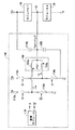
図1A及び1Bにおいて、この発明では、実質的な寄生抵抗の壁を克服するべく、デバイス群(例えば、複合論理回路マクロ及び/又はモジュール)を互いに上に積み重ねる。図1Aでは、複合論理回路マクロ20及び24は、他の一方の上に積み重ねられ、VDD及びVLの間に接続されている。ある実施例では、VLはグラウンドであってよい。図1Bでは、モジュール30及び34が他の一方に積み重ねられ、VDD及びVLの間に接続されている。もし複合論理回路マクロ20及び24、或いはモジュール30及び34の複雑さがおよそ同じ2つの部分に分けられ、半分のそれぞれが略等価に動作するなら、電流要件は積み重ねられていないデバイスの約半分となる。
In FIGS. 1A and 1B, the present invention stacks devices (eg, complex logic macros and / or modules) on top of each other to overcome substantial parasitic resistance barriers. In FIG. 1A,
積み重ねられたデバイスは、積み重ねられていないデバイスの2倍の電圧で動作する。しかしながら、複合論理回路マクロ20及び24、或いはモジュール30及び34が実質的に同じ電流レベルを消費するという保証はない。これは、それぞれが実質的に同じ電流量を吸収するように作られない限り、解決不可能な問題のように思われる。半分のそれぞれがデバイス全体に印加された全電圧の半分を降下させることを、現実的に保証する方法はない。
Stacked devices operate at twice the voltage of unstacked devices. However, there is no guarantee that the
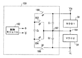
図2A及び2Bでは、この発明における電流バランスモジュール50は、VDD、VL、及び/又は論理回路マクロ20及び24或いはモジュール30及び34の間のノード52の少なくともひとつに接続される。電流バランスモジュール50は、論理回路マクロ20及び24、或いはモジュール30及び34に供給される電流量を均衡させようとする。特に、電流バランスモジュール50は、図2Aにおける複合論理回路マクロ20及び24のそれぞれ、或いは図2Bにおけるモジュール30及び34のそれぞれに、(VDD−VL)の約1/2を供給する。典型的な電流バランスモジュール50は、以下に記載されるような、バックコンバータ、2:1DC/DCコンバータ、線形プッシュプルレギュレータ、低ドロップアウト(LDO)レギュレータ、平衡スイッチキャパシタンスデバイス、スイッチインダクタデバイス、キャパシタ/インダクタデバイス、ヒステリシスコンパレータ、及び/又は他の同様のデバイスを含む。
2A and 2B, the
図3A及び3Bでは、積み重ねられた複数の複合論理回路マクロ又はモジュールが、バックコンバータ68による均衡化とともに示される。バックコンバータ68は、図3A及び図3Bに示されるトポロジ、及び/又は他の適切なトポロジを持つことができる。バックコンバータ68は、伝導スイッチ70及びフリーホイールスイッチ72を含む。制御モジュール73は、スイッチ70及び72への駆動信号を生成する。制御モジュール73は、ノード52における電圧及び/又は電流を検出して、それらに基づいて複数のスイッチを制御する。ある実施例では、スイッチ70及び72は反対の状態を持つ。インダクタンス素子78は、スイッチ70及び72の間に接続された1つの端と、複合論理回路マクロ20及び24或いはモジュール30及び34と接続された反対の端を持つ。バックコンバータ68は、均衡化をもたらすべく電流を吸収又は供給する。
In FIGS. 3A and 3B, a plurality of stacked complex logic macros or modules are shown with balancing by the
図4A及び4Bでは、2つのそれぞれの電圧が略同一になるように、2つの間で電流を均衡化させる1つの実施例が示されている。図4Aでは、結合インダクタ104を利用した2:1DC/DCコンバータ100によって均衡化動作が得られる。動作上の更なる詳細は、2003年10月24日に出願された米国特許出願番号10/693787、”Voltage Regulator”に記載され、参考のため本願に全文を引用する。
In FIGS. 4A and 4B, one embodiment is shown that balances the current between the two so that the two respective voltages are substantially identical. In FIG. 4A, a balancing operation is obtained by the 2: 1 DC /
2:1DC/DCコンバータ100は、1つの入力電圧VDDから1つの出力電圧VOUTを生成すべく、180度離れた位相で動作する2つのバックコンバータを含む。それぞれのバックコンバータは、条件スイッチ110a又は110b、フリーホイールスイッチ114a又は114b、並びにインダクタ140a又は140bを含む。1つの出力キャパシタンス118は、それぞれのバックコンバータの出力電圧をフィルタする。リップル電流は無視できるので出力キャパシタンス118の値を小さくすることができる。また、2:1DC/DCコンバータ100の入力と出力との間が強く結合しているので、入力におけるいずれの容量も、出力において負荷に並列容量を効果的に供給するよう出力キャパシタ118と連携して動作する。1つの制御モジュール119は、110a、110b、114a、及び114bへの駆動信号を生成する。制御モジュール119は、ノード52における電圧又は電流を検出して、それらに基づいて複数のスイッチを制御する。
The 2: 1 DC /
スタートアップ回路130は、スタートアップの間にわたってノード52がVDDより小さい電圧に維持されることを保証すべく、必要に応じて備えられる。ある実施例においては、そのノードは、スタートアップの間およそVDD/2に維持される。ある実施例においては、スタートアップ回路130は、1つかそれより多いキャパシタを含む。他にも、複数のモジュールの両端の超過電圧を防ぎ、スタートアップの間にわたってノード52がおよそVDD/2に維持される、及び/又はVDDより小さい閾電圧VTHより小さい電圧であることの少なくとも一方であることを保証すべく、スタートアップの間にわたってVDDを増加又は掃引させることができる。閾値VTHは、複数のマクロ又はモジュールに損害を与える電圧より低い電圧であるべきである。
A start-up
図4Bでは、図4Aに示す出力キャパシタンス118が118Bとして符号が付されている。複数のマクロ及び/又はモジュールがスタートアップの間にわたってVTHを超える電圧を受けないように、及び/又はおよそVDD/2となるように、他のキャパシタンス118Aを必要に応じて加えることができる。また、複数のマクロ又はモジュールの両端の超過電圧を防ぐために、VDDはスタートアップの間にわたって増加又は掃引されてよい。また、スタートアップの間にわたって電圧を制限する他の方法を用いることができる。ある実施例においては、複数のキャパシタンスの電気容量は実質的に同じに設定される。
In FIG. 4B, the
ある実施例では、インダクタ104a及び104bは互いに強く結合されていて、結合係数Kは約1である。インダクタ104a及び104bは、インダクタ104a及び104bの間の高い結合係数を備えるインダクタアセンブリ104を形成すべく、磁気コアに共に巻かれている。複数のインダクタ巻線の極性は、インダクタ104aおよび104bを流れる直流電流がほぼ打ち消され、インダクタアセンブリ104の磁気コアを流れる直流電流がおよそ零になるように選択される。したがって、低透磁率の材料のより小さいコアサイズがインダクタ104a及び104bに用いられ、結果としてより小さいサイズ(体積)でより低コストのインダクタアセンブリ104に結びつく。さらに、2:1DC/DCコンバータ100の過渡応答は、過渡負荷電流に関する限り、個々のインダクタンスの打ち消しによって改善される。
In one embodiment,
積み重ねられた複合論理回路マクロ20及び24、或いはモジュール30及び34のノード52に流れ込むかノード52から流れ出るかにかかわらず、いずれの超過電流も、2:1DC/DCコンバータ100に吸収され95%近い効率で主電源に戻される。スタートアップ後には、2:1DC/DCコンバータ100は、複合論理回路マクロ20及び24或いはモジュール30及び34のそれぞれにかかる電圧が略同一となることを保証する。半分のそれぞれが電流レベルにおいてせいぜい25%の不一致があることを仮定すると、2:1DC/DCコンバータ100は、全デバイスの半分の電流の25%、すなわち全電流の1/8を吸収又は供給する必要がある。
Regardless of whether they flow into or out of
元々100Aの電流要件を持つマイクロプロセッサの例に戻ると、2:1DC/DCコンバータ100は、全電流の12.5Aより小さい電流を吸収又は供給する必要がある。これは、下記図13A−13Cで示されるような、マイクロプロセッサダイ内の集積パワーMOSFET及びマイクロプロセッサパッケージの下に設けられた1つの1:1結合インダクタ104を用いて容易に製造することができる。
Returning to the example of a microprocessor with a current requirement of 100A originally, the 2: 1 DC /
他の適切なバックコンバータ及び2:1コンバータのトポロジは、2004年3月26日に出願された米国特許出願番号10/810452、”Voltage Regulator”、2003年10月24日に出願された米国特許出願番号10/693787、”Voltage Regulator”、及び2004年1月8日に出願された米国特許出願番号10/754187、”Digital Low Dropout Regulator”に示されて説明されており、参考のため本願にそれらの全文を引用する。 Other suitable buck converters and 2: 1 converter topologies are described in US patent application Ser. No. 10/810452, filed Mar. 26, 2004, “Voltage Regulator”, US patent filed on Oct. 24, 2003. No. 10/693787, “Voltage Regulator”, and US patent application Ser. No. 10/754187, filed Jan. 8, 2004, “Digital Low Dropout Regulator”, described in this application for reference. Cite their full text.
図5A及び5Bでは、複合論理回路マクロ20及び24或いはモジュール30及び34の積み重ねは、高い消費電力の半導体デバイスにとって有用なだけでなく、個人用の情報端末(PDA)、MP3プレーヤ、携帯衛星ラジオ、携帯電話等のハンドヘルドマーケットで使用されることを目的にした低消費電力の集積回路にとっても有用である。多くのハンドヘルド用途では、最近の半導体デバイスを駆動するのに要求される異なる複数の低い電圧供給レベルを生成するために、限られた数のDC/DCコンバータしか使用することができない。
In FIGS. 5A and 5B, stacking of
複合論理回路マクロ20及び24、並びにモジュール30及び34を積み重ねることは、2つの複合論理回路マクロ又はモジュールが低電圧で動作することができる用途、及び積み重ねられて合算された電圧が集積回路の1つのアナログ部分を動作させるのに既に利用可能である用途に適切である。例えば、1.8Vのアナログ電圧が供給されるデバイスは、それぞれ0.9Vで動作する組み込み論理回路の半分のそれぞれに電力を供給するために使用することができる。それぞれの間の電流の不一致は依然として対処される必要がある。
Stacking
この場合、図5A及び5Bに示されるように、2つのそれぞれの間で電流を行き来させるのに平衡スイッチキャパシタンスデバイス150を使用することができる。制御モジュール154は、ノード164における電流及び/又は電圧を検知して、キャパシタC1及びC2の充電及び放電を変えるべくスイッチ158及び160を制御する。平衡キャパシタC1及びC2の切り替え動作は、2つの半分のそれぞれの電流要件にアンバランスがある場合でも、それぞれの電圧が略同一となることを保証するために用いられる。ある実施例においては、スタートアップの間にわたったモジュール20及び24の両端にかかる超過電圧を防ぐために、C1の容量はC2の容量と実質的に等価に設定される。言い換えると、ノード164は、スタートアップの間にわたってVTHより小さく及び/又はVDD/2と略同一に維持される。図では、平衡スイッチキャパシタンスデバイスが示されているが、当業者は、スイッチインダクタンスデバイス及び/又はスイッチキャパシタンス/インダクタンスデバイスを用いることができることを理解するであろう。
In this case, a balanced
図6A及び6Bでは、キャパシタC1、C2、及びC3、並びにスイッチ180、182、184、及び186を含む他の平衡スイッチキャパシタンスデバイスが示されている。スイッチキャパシタモジュール192は、ノード192から電流を吸収又は供給すべくスイッチ180〜186を制御する。ある実施例においては、スイッチ180及び184はペアで切り替えられ、スイッチ182及び186がペアで切り替えられ、反対の状態を持つ。スイッチキャパシタンスモジュール190は、ノード192の電流又は電圧を検知して、その結果に基づいて複数のスイッチを制御する。平衡キャパシタC1、C2、及びC3の切り替え動作は、それぞれの間で電流要件にアンバランスがある場合でも、それぞれの電圧が略同一となることを保証するために使用される。
In FIGS. 6A and 6B, other balanced switch capacitance devices including capacitors C 1 , C 2 , and C 3 and switches 180, 182, 184, and 186 are shown.
図7A及び7Bでは、線形プッシュプルレギュレータ200が、いくらかの効率低下とともに使用される。半分のそれぞれが相対的に均衡するように設計されれば、効率の低下は最小限となる。この方法は、典型的には50%の効率しか持たない線形レギュレータより著しく良く機能する。それでも、ある実施例では複数の線形レギュレータを使用することもできる。
In FIGS. 7A and 7B, a linear push-
線形プッシュプルレギュレータ200は、それぞれトランジスタT1及びT2の制御端子と連通する出力端子を持つ第1オペアンプ204及び第2オペアンプ208を含む。ある実施例では、トランジスタT1及びT2はCMOSトランジスタである。トランジスタT1の第1端子はVDDに接続される。トランジスタT1の第2端子は、トランジスタT2の第1端子に接続される。トランジスタT2の第2端子はVLに接続される。オペアンプ204の非反転入力は、上限の電圧閾値VULに接続され、オペアンプ208の非反転入力は下限の電圧閾値VLLに接続される。オペアンプ208の反転入力は、オペアンプ204の反転入力に接続され、抵抗Rの一端に接続される。抵抗Rの他端は、第1及び第2トランジスタT1及びT2のそれぞれ第2及び第1端子に接続される。第1及び第2トランジスタT1及びT2のそれぞれ第2及び第1端子は、図7Aにおける第1及び第2論理回路マクロ20及び24の間、若しくは、図7Bにおける第1及び第2モジュール30及び34の間のノード210に接続される。
The linear push-
ノード210が目標電圧(VDD−VL)/2より小さく第1の閾値(VUL−(VDD−VL)/2)までの場合、上方の論理回路マクロ又はモジュールは電圧を大きく降下している。上方のオペアンプ204は、ノード210にVDDを印加するトランジスタT1を瞬間的にオンにする。ノード210におけるVDDは、論理回路マクロ24又はモジュール34の両端の電圧を引き上げ、論理回路マクロ20又はモジュール30の両端の電圧を押し下げる。ノード210にVDDが印加されると、オペアンプ204はT1をオフにし、このプロセスは電圧の違いが第1閾値より小さくなるまで繰り返される。
When the
ノード210が目標電圧(VDD−VL)/2より大きく第2の閾値(VUL−(VDD−VL)/2)までの場合、下方の論理回路マクロ又はモジュールは電圧を大きく降下している。下方のオペアンプ208は、ノード210にVLを印加するトランジスタT2を瞬間的にオンにする。ノード210におけるVLは、論理回路マクロ20又はモジュール30の両端の電圧を引き上げ、論理回路マクロ24又はモジュール34の両端の電圧を押し下げる。ノード210にVLが印加されると、オペアンプ208はT2をオフにし、このプロセスは電圧の差が第1の閾値より小さくなるまで繰り返される。
When the
理解できるように、様々なタイプのレギュレータを使用することができる。上記に記載された実施例に加えて、他のタイプのDC/DCコンバータ、プッシュプルレギュレータ、スイッチキャパシタンスデバイスを使用することができる。また、これに限定されるものではないが、ヒステリシスコンパレータを含む他のタイプのレギュレータを使用することができる。例えば、適切なヒステリシスコンパレータは、2003年6月23日に出願された米国特許出願番号10/602997、”Simplified Comparator with Digitally Controllable Hysteresis and Bandwidth”に示されて説明されたヒステリシスコンパレータを含み、参考のため本願に当該出願の全文を引用する。 As can be appreciated, various types of regulators can be used. In addition to the embodiments described above, other types of DC / DC converters, push-pull regulators, and switch capacitance devices can be used. Also, other types of regulators including, but not limited to, hysteresis comparators can be used. For example, suitable hysteresis comparators include those illustrated and described in US patent application Ser. No. 10 / 602,997 filed Jun. 23, 2003, “Simplified Comparator with Digitally Controllable Hysteresis and Bandwidth”. Therefore, the full text of the application is cited in the present application.
図7Bでは、第1キャパシタンスC1及び第2キャパシタンスC2が、スタートアップの間にわたってモジュール30及び34の両端の電圧をVTHより小さくVDD/2に略等しく制限すべく設けられる。ある実施例においては、キャパシタンスC1の電気容量はC2の電気容量と実質的に同じである。言い換えると、ノード210はスタートアップの間にわたっておよそVDD/2に維持される。
7B, the first capacitance C 1 and the second capacitance C 2 is provided so as to substantially equally limit the voltage across the
図8A及び8Bでは、ヒステリシスコンパレータ250及び254が、論理回路マクロ20及び24、若しくはモジュール30及び34の両端の電圧を調整すべく使用される。コンパレータ250は、VDD、上方の閾値電圧VUL、及びノード210における電圧を受け取る。ある実施例では、コンパレータ250は、固定又は可変のオフセット256、固定又は可変の帯域幅258、及び/又は、固定又は可変のディレイ260を有する。可変である場合、コンパレータ254は、それぞれの調整を行うべく1以上の対応する入力を受け取る。コンパレータ254はVL、下限の電圧閾値VLL、及びノード210における電圧を受け取る。
In FIGS. 8A and 8B,
ノード210が目標電圧(VDD−VL)/2より小さく上限の閾値(VUL−(VDD−VL)/2)までの場合、上方の論理回路マクロ又はモジュールは電圧を大きく降下している。コンパレータ250はノード210にVDDを印加する。ノード210におけるVDDは、論理回路マクロ24又はモジュール34の両端の電圧を引き上げ、論理回路マクロ20又はモジュール30の両端の電圧を押し下げる。VDDがノード210に遅延期間の間印加されると、コンパレータ250はノード210へのVDDの印加を停止する。このプロセスは差が上限の閾値より小さくなるまで繰り返される。
When the
ノード210が目標電圧(VDD−VL)/2より大きく下限の閾値((VDD−VL)/2−VUL)までの場合、下方の論理回路マクロ又はモジュールは電圧を大きく降下している。コンパレータ254はノード210にVLを印加する。ノード210におけるVLは、論理回路マクロ20又はモジュール30の両端の電圧を引き上げ、論理回路マクロ24又はモジュール34の両端の電圧を押し下げる。ノード210にVLが遅延期間の間印加されると、コンパレータ254はノード210へのVLの印加を停止する。このプロセスは差が下限の閾値より小さくなるまで繰り返される。
When the
論理回路マクロ及びモジュールの2段積みが示されているが、それに加えて、当業者は更なるレベルの積み重ねを用いることができることを理解できるだろう。また、他の均衡化の方法を用いることができる。 Although a two-stage stack of logic macros and modules is shown, in addition, those skilled in the art will appreciate that additional levels of stacking can be used. Other balancing methods can also be used.
図9Aでは、DC/DCコンバータ300は、入力信号を受信し、4V及び25Aの出力を生成する。第1の2:1コンバータ304は、4V、25Aの入力を、2V、50Aの出力に変換する。第2コンバータ308は、2V、50Aの入力を1V、100Aの出力に変換する。プリント基板回路(PCB)314上に実装されたマクロ又はモジュール312は、抵抗310(これは線及び他の結線の寄生抵抗を示す)を介して2:1コンバータ308の出力に接続されてよい。理解できるように、寄生抵抗310による損失はI2Rに等しい。ここで、Iは寄生抵抗Rを流れる電流の強さである。図9Bについて、この発明によると、上記の324及び328で示されるマクロ又はモジュールのペアの間に2:1コンバータ320(又は他の電流バランスモジュール)を接続することによって、損失を1/4に減少させるができる。
In FIG. 9A, a DC /
図9Cでは、更なる複数のモジュールは更なる複数の2:1コンバータと結合されてよい。図9Cでは、4つのモジュール又はマクロ340、342、344、及び346が直列に接続され、間にノード347、348、及び349を持つ。第1の2:1コンバータ330は、DC/DCコンバータ300の出力と、マクロ又はモジュール340と、ノード348とに接続されている。ノード348は、2:1コンバータ334及び336と、モジュール又はマクロ342及び344とにも接続されている。図示されるように、2:1コンバータ334は、DC/DCコンバータ300の出力と、モジュール又はマクロ340と、ノード347及び348とにも接続されている。図示されるように、2:1コンバータ336は、ノード348及び349にも接続されている。2:1コンバータ320は、PCBを流れる全電流を制御する2:1コンバータ308より小型にすることができる。対照的に、2:1コンバータ320は、積み重ねられた複数のデバイスの間の電流の不一致を制御するだけでよい。
In FIG. 9C, additional modules may be combined with additional multiple 2: 1 converters. In FIG. 9C, four modules or
より一般的には、回路に2n個のモジュール又はマクロが含まれる場合、回路は2n−1個の2:1DC/DCコンバータを含む。複数の2:1DC/DCコンバータはn個の分岐線に配置される。2n−1個の2:1DC/DCコンバータは、隣接するDC/DCコンバータの間に2n−1個のノードを持つ。それぞれの2n−1個のDC/DCコンバータは、2n−1個のノードのうちのそれぞれ1つと接続される。 More generally, if it contains the 2 n modules or macros circuit, the circuit is 2 n -1 2: containing 1 DC / DC converter. A plurality of 2: 1 DC / DC converters are arranged on n branch lines. A 2 n -1 2: 1 DC / DC converter has 2 n -1 nodes between adjacent DC / DC converters. Each 2 n −1 DC / DC converter is connected to a respective one of 2 n −1 nodes.
例えば図9Cでは、2つの分岐線350及び352が存在する。第1分岐線350は1つの2:1コンバータを含み、第2分岐線は2つの2:1DC/DCコンバータを含む。より一般的には、第1分岐線は20=1個の2:1DC/DCコンバータを含み、第2分岐線は21=2個の2:1DC/DCコンバータを含み、第3分岐線は22=4個の2:1DC/DCコンバータを含み・・・、n番目の分岐線は2n−1個の2:1DC/DCコンバータを含む。
For example, in FIG. 9C, there are two
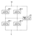
図10A及び10Bでは、ルータ、スイッチ、又は他のネットワークデバイスのような通信デバイス360は、典型的に複数の通信チャネル364−1、364−2、364−3、及び364−4(チャネル364と総称する。)を含む。4つのシグナルプロセッサモジュールしか示されていないが、シグナルプロセッサの更なるペアを用いることができる。それぞれのチャネル364は、シグナルプロセッサ366−1、366−2、366−3、及び366−4(シグナルプロセッサ366と総称する。)を含む。それぞれのシグナルプロセッサ366は典型的には同じ設計であり、シグナルプロセッサモジュール366は動作時に略同一の電流量を消費し易い。上記又は下記のような電流バランスモジュール370は、電流消費の差を均衡すべく設けられる。不一致を低減させるという理由から、線形LDOレギュレータのような低効率のデバイスを使用してよい。とはいえ、他の電流バランスモジュールを使用してもかまわない。例えば、通信チャネルは、1000Base−Tイーサネット、10GBase−Tイーサネット、若しくは他の現在又は将来のイーサネット、或いは他の規格に準拠してよい。
10A and 10B, a
図11A及び11Bでは、グラフィックスプロセッシングユニット(GPU)380は、複数のグラフィックスパイプラインモジュール382−1、382−2、・・・、及び382−N(グラフィックスパイプラインモジュール382と総称する。)を含む。それぞれのグラフィックスパイプラインモジュール382は同じ設計を持つので、グラフィックスパイプラインモジュール382は動作時に同量の電流を消費し易い。上記又は下記のような電流バランスモジュール390が、電流消費の差を調整すべく設けられる。
11A and 11B, the graphics processing unit (GPU) 380 includes a plurality of graphics pipeline modules 382-1, 382-2,..., And 382-N (collectively referred to as graphics pipeline module 382). Including. Since each
図12では、第1プロセッサ400及び第2プロセッサ402は、第1プロセッサ400及び第2プロセッサ402の電流消費を調整するパワー調整モジュール404と通信する。ある実施例においては、パワー調整モジュール404はハードウェアベース、ソフトウェアベース、及び/又はハードウェア及びソフトウェアベースであってよい。ある実施例においては、パワー調整モジュール404は、電流消費のバランスをとるために、第1及び第2プロセッサの相対的な動作周波数を調整する。パワー調整モジュール404は、電流消費のバランスをとるために、第1プロセッサ400及び第2プロセッサ402のロードバランシング及び/又はスロットリングを使用してよい。ある実施例においては、パワー調整モジュール404は、上記及び下記のような任意の電流バランスモジュール406と組み合わせて用いられる。言い換えると、パワー調整モジュール404は大まかな均衡化を行い、電流バランスモジュールは細かな電流の均衡化を行う。
In FIG. 12, the
図13A、13B、及び13Cでは、パワー管理モジュール404は周波数バランスモジュール404’を含む。更に電流消費を均衡化すべく、任意の2:1DC/DCコンバータ406’を使用することができる。図13Bには、半導体ダイ408の上に作られた、第1プロセッサ400、第2プロセッサ402、及び2:1DC/DCコンバータ406’の典型的な配置が示されている。図13Cでは、図13Bの半導体ダイ408は、PCB412上に配置された第1ソケット411及び第2ソケット416によってPCB412に接続されている。ある実施例においては、2:1DC/DCコンバータ406に関連する上記のインダクタ420及び422が、半導体ダイ408及びPCB412の間に配置される。複数のピン426がダイ408から延伸しており、それらはソケット411及び416に収容される。パワー管理モジュール404が周波数バランスモジュール404’を含むように示されているが、当業者は、上記及び/又は下記の様々な方法によって、ハードウェア及び/又はソフトウェアによる電流均衡化が行われることを理解するだろう。
In FIGS. 13A, 13B, and 13C, the
図14では、パワー調整モジュール404はオペレーティングシステム404’’を含む。OS404’’又はチップは、第1プロセッサ400及び第2プロセッサ402に複数のスレッドを割り当てることによって、負荷均衡化を行うことができる。OS404’’又はチップは、電流のアンバランスを小さくすべく、第1プロセッサ400及び/又は第2プロセッサ402を抑制することができる。例えば、CPUスピードは次のように設定される。

それぞれのCPUを最大周波数の1/2で動作させると、それぞれのCPUはより低い電圧で動作することができるので、より効果的である。ある実施例では、他のCPUの電流消費と均衡化させるべく、複数のCPUのうちの1つの動作周波数が低下及び/又は増加させられる。代わりに、他に生じる電流のアンバランスを均衡化させるために、複数のCPUの少なくとも1つにダミーオペレーションを実行させることができる。 Operating each CPU at half the maximum frequency is more effective because each CPU can operate at a lower voltage. In one embodiment, the operating frequency of one of the CPUs is reduced and / or increased to balance the current consumption of other CPUs. Instead, at least one of the CPUs can perform a dummy operation to balance the current imbalance that occurs elsewhere.
図4A、4B、5A,及び7Bに戻ると、複数のマクロ及び/又はモジュールの間のノードにおける電圧がスタートアップの間にわたってVTHより低く及び/又はおよそVDD/2に維持されることを確実にすべく、回路及び/又はキャパシタが用いられた。当業者は、ここに示されて説明された他の実施例が、複数のマクロ及び/又はモジュールの間のノードにおける電圧をスタートアップの間にわたってVTHより低く及び/又はおよそVDD/2に維持するための複数の回路及び/又はキャパシタを含むことを理解するであろう。 Returning to FIGS. 4A, 4B, 5A, and 7B, ensure that the voltage at the node between the multiple macros and / or modules is maintained below V TH and / or approximately at V DD / 2 during startup. In order to achieve this, circuits and / or capacitors were used. Those skilled in the art will appreciate that other embodiments shown and described herein maintain the voltage at the node between multiple macros and / or modules below V TH and / or approximately V DD / 2 during startup. It will be understood that a plurality of circuits and / or capacitors for doing so are included.
当業者は、本発明に関する広い教示を様々な形態で実装できることを、上述の説明から理解できるであろう。したがって、特定の例に関連付けて本発明を説明したが、当業者にとって図面、明細書、および特許請求の範囲の検討に基づいて他の変形も明らかであるから、本発明の真の範囲は上述の説明に限定して解釈されるべきではない。 Those skilled in the art can now appreciate from the foregoing description that the broad teachings of the invention can be implemented in a variety of forms. Thus, although the invention has been described with reference to specific examples, the true scope of the invention has been described above since other variations will be apparent to one of ordinary skill in the art upon review of the drawings, specification, and claims. It should not be construed as being limited to the description.
本発明は、詳細な説明及び添付図面からさらに完全に理解されるだろう。
Claims (12)
前記2n個のモジュールの隣接する複数のモジュールの間に配置された2n−1個のノードと、
2n−1個の2:1DC/DCコンバータであって、それぞれの前記2n−1個の2:1DC/DCコンバータは、前記2n−1個のノードのうちのそれぞれ1つと連通する2n−1個の2:1DC/DCコンバータと
を備え、
前記nは2以上の整数である回路。 2 n modules connected in series between the first and second reference potentials;
2 n −1 nodes disposed between a plurality of adjacent modules of the 2 n modules;
2 n -1 2: 1 DC / DC converters, each of the 2 n -1 2: 1 DC / DC converters being in communication with a respective one of the 2 n-1 nodes. n- 1 2: 1 DC / DC converters,
The circuit wherein n is an integer of 2 or more.
請求項1に記載の回路。 The circuit of claim 1, wherein the 2 n −1 2: 1 DC / DC converters are arranged on n branch lines.
請求項2に記載の回路。 The first branch line has one of the 2 n -1 2: 1 DC / DC converters, and the second branch line is two of the 2 n -1 2: 1 DC / DC converters. the a, the n branch lines the 2 n -1 2: the circuit of claim 2 having 2 n-1 pieces of 1 DC / DC converter.
請求項1に記載の回路。 The circuit of claim 1, wherein the plurality of modules includes a plurality of composite logic circuit macros.
請求項1に記載の回路。 The circuit of claim 1, wherein the plurality of modules include a plurality of application specific integrated circuits (ASICs).
請求項1に記載の回路。 The circuit of claim 1, wherein the plurality of modules includes a plurality of processing modules.
2n個のモジュールの隣接する複数のモジュールの間に配置される2n−1個のノードを提供する段階と、
変換のための2n−1個の2:1DC/DCコンバータを提供する段階であって、それぞれの前記2n−1個の2:1DC/DCコンバータは、前記2n−1個のノードのうちのそれぞれ1つと連通する段階と
を備え、
前記nは2以上の整数である、回路を製造する方法。 Providing 2 n modules connected in series between first and second reference potentials;
Providing 2 n −1 nodes disposed between adjacent modules of 2 n modules;
Providing 2 n -1 2: 1 DC / DC converters for conversion, each of the 2 n -1 2: 1 DC / DC converters being connected to the 2 n-1 nodes. Each communicating with one of them,
The method for manufacturing a circuit, wherein n is an integer of 2 or more.
請求項7に記載の方法。 The method of claim 7, wherein the 2 n -1 2: 1 DC / DC converters are arranged in n branch lines.
請求項8に記載の方法。 The first branch line has one of the 2 n -1 2: 1 DC / DC converters, and the second branch line is two of the 2 n -1 2: 1 DC / DC converters. having a n-th branch includes the 2 n -1 pieces of 2: 1 DC / method according to claim 8 having 2 n-1 pieces of DC converters.
請求項7に記載の方法。 The method of claim 7, wherein the 2 n modules include a plurality of composite logic macros.
請求項7に記載の方法。 The method of claim 7, wherein the 2 n modules comprise a plurality of application specific integrated circuits (ASICs).
請求項7に記載の方法。 The method of claim 7, wherein the 2 n modules include a plurality of processing modules.
Applications Claiming Priority (8)
| Application Number | Priority Date | Filing Date | Title |
|---|---|---|---|
| US63155204P | 2004-11-29 | 2004-11-29 | |
| US60/631,552 | 2004-11-29 | ||
| US66393305P | 2005-03-21 | 2005-03-21 | |
| US60/663,933 | 2005-03-21 | ||
| US11/098,129 US7594127B2 (en) | 2004-11-29 | 2005-04-04 | Low voltage logic operation using higher voltage supply levels |
| US11/098,129 | 2005-04-04 | ||
| US11/179,106 | 2005-07-12 | ||
| US11/179,106 US7702929B2 (en) | 2004-11-29 | 2005-07-12 | Low voltage logic operation using higher voltage supply levels |
Publications (2)
| Publication Number | Publication Date |
|---|---|
| JP2006203169A JP2006203169A (en) | 2006-08-03 |
| JP5036171B2 true JP5036171B2 (en) | 2012-09-26 |
Family
ID=36021750
Family Applications (2)
| Application Number | Title | Priority Date | Filing Date |
|---|---|---|---|
| JP2005332228A Active JP5036171B2 (en) | 2004-11-29 | 2005-11-16 | Low voltage logic circuit operation with high voltage supply level |
| JP2005332227A Active JP4690177B2 (en) | 2004-11-29 | 2005-11-16 | Low voltage logic circuit operation with high voltage supply level |
Family Applications After (1)
| Application Number | Title | Priority Date | Filing Date |
|---|---|---|---|
| JP2005332227A Active JP4690177B2 (en) | 2004-11-29 | 2005-11-16 | Low voltage logic circuit operation with high voltage supply level |
Country Status (4)
| Country | Link |
|---|---|
| US (1) | US7702929B2 (en) |
| EP (2) | EP1662643B1 (en) |
| JP (2) | JP5036171B2 (en) |
| TW (2) | TWI400867B (en) |
Families Citing this family (29)
| Publication number | Priority date | Publication date | Assignee | Title |
|---|---|---|---|---|
| US7639927B2 (en) * | 2004-09-14 | 2009-12-29 | Marvell World Trade Ltd. | Unified control and memory for a combined DVD/HDD system |
| US7594127B2 (en) * | 2004-11-29 | 2009-09-22 | Marvell World Trade Ltd. | Low voltage logic operation using higher voltage supply levels |
| US7788510B2 (en) * | 2004-11-29 | 2010-08-31 | Marvell World Trade Ltd. | Low voltage logic operation using higher voltage supply levels |
| US7710895B2 (en) * | 2007-03-14 | 2010-05-04 | Broadcom Corporation | Selective mode PHY device and method for managing power utilization using same |
| US20080259797A1 (en) * | 2007-04-18 | 2008-10-23 | Aladdin Knowledge Systems Ltd. | Load-Balancing Bridge Cluster For Network Nodes |
| US8476962B2 (en) * | 2009-11-18 | 2013-07-02 | Freescale Semiconductor, Inc. | System having multiple voltage tiers and method therefor |
| US8169257B2 (en) * | 2009-11-18 | 2012-05-01 | Freescale Semiconductor, Inc. | System and method for communicating between multiple voltage tiers |
| KR101890946B1 (en) * | 2012-06-14 | 2018-08-22 | 주식회사 두산 | Power Supplies Conversion System of Engine Forklift Truck |
| US8861145B2 (en) * | 2012-07-19 | 2014-10-14 | Honeywell International Inc. | Circuit with motor driver spike suppression |
| KR101350388B1 (en) * | 2012-11-22 | 2014-01-15 | 숭실대학교산학협력단 | Integrated circuit having stack structure |
| US9513644B1 (en) * | 2013-01-16 | 2016-12-06 | Maxim Integrated Products, Inc. | Energy efficient systems having linear regulators and methods of operating the same |
| KR102107076B1 (en) * | 2013-12-02 | 2020-05-08 | 에스케이하이닉스 주식회사 | Semiconductor apparatus |
| US9564794B2 (en) * | 2013-12-04 | 2017-02-07 | Broadcom Corporation | System, apparatus, and method for a ping-pong charge pump |
| US20150168973A1 (en) * | 2013-12-18 | 2015-06-18 | Hashfast LLC | Stacked chips powered from shared voltage sources |
| WO2015120306A2 (en) * | 2014-02-07 | 2015-08-13 | The Trustees Of Dartmouth College | System and method for reducing power loss in switched-capacitor power converters |
| JPWO2016121273A1 (en) * | 2015-01-30 | 2017-11-02 | ソニー株式会社 | Power control apparatus, power control method, and power control system |
| US10033272B2 (en) * | 2015-03-12 | 2018-07-24 | Qualcomm Incorporated | Switching loss correction circuitry and method |
| US9917588B2 (en) | 2015-07-08 | 2018-03-13 | Nxp B.V. | Level shifter and approach therefor |
| US9912335B2 (en) | 2015-07-08 | 2018-03-06 | Nxp B.V. | Configurable power domain and method |
| US9960769B2 (en) | 2015-12-17 | 2018-05-01 | Nxp B.V. | Power-domain optimization |
| US9514264B1 (en) | 2016-01-05 | 2016-12-06 | Bitfury Group Limited | Layouts of transmission gates and related systems and techniques |
| US9660627B1 (en) | 2016-01-05 | 2017-05-23 | Bitfury Group Limited | System and techniques for repeating differential signals |
| US9645604B1 (en) | 2016-01-05 | 2017-05-09 | Bitfury Group Limited | Circuits and techniques for mesochronous processing |
| US9614526B1 (en) | 2016-02-09 | 2017-04-04 | Nxp B.V. | Power-domain assignment |
| US9960670B2 (en) | 2016-03-11 | 2018-05-01 | Nxp B.V. | Apparatus for charge recycling |
| US10158292B2 (en) | 2017-01-23 | 2018-12-18 | Nxp B.V. | Power configuration |
| US10270448B1 (en) | 2018-05-16 | 2019-04-23 | Nxp B.V. | Level shifter circuit with transistor drive strength variation compensation |
| TWI664811B (en) * | 2018-12-14 | 2019-07-01 | Giga-Byte Technology Co.,Ltd. | Power regulator and power regulating method |
| CN117616680A (en) * | 2021-12-14 | 2024-02-27 | 华为技术有限公司 | Balancer circuit for series connection of two DC link capacitors, method for controlling balancer circuit, and converter device |
Family Cites Families (26)
| Publication number | Priority date | Publication date | Assignee | Title |
|---|---|---|---|---|
| SE8605266L (en) * | 1986-12-09 | 1988-06-10 | Ragnar Jonsson | SWITCH CONNECTION |
| US5079441A (en) * | 1988-12-19 | 1992-01-07 | Texas Instruments Incorporated | Integrated circuit having an internal reference circuit to supply internal logic circuits with a reduced voltage |
| JPH03163864A (en) * | 1989-11-22 | 1991-07-15 | Hitachi Ltd | Hierarchical power supply type integrated circuit |
| US5204809A (en) * | 1992-04-03 | 1993-04-20 | International Business Machines Corporation | H-driver DC-to-DC converter utilizing mutual inductance |
| JPH07273286A (en) * | 1994-03-28 | 1995-10-20 | Yamaha Corp | Semiconductor integrated circuit |
| EP0721137B1 (en) | 1994-07-14 | 2004-01-21 | Seiko Epson Corporation | Power source circuit, liquid crystal display device, and electronic device |
| US6311214B1 (en) * | 1995-07-27 | 2001-10-30 | Digimarc Corporation | Linking of computers based on optical sensing of digital data |
| US5631534A (en) * | 1995-08-21 | 1997-05-20 | Delco Electronics Corp. | Bidirectional current pump for battery charge balancing |
| JPH10163842A (en) * | 1996-11-25 | 1998-06-19 | Fujitsu Ltd | Semiconductor integrated circuit |
| GB2374991B (en) | 1998-05-07 | 2002-12-18 | Ford Motor Co | Battery charge balancing system |
| WO2000049511A1 (en) * | 1999-02-17 | 2000-08-24 | Sony Corporation | Semiconductor ic, information processing method, information processing device, and program storage medium |
| FR2800955B1 (en) | 1999-11-04 | 2005-04-29 | Cit Alcatel | METHOD FOR TELE-POWERING A TERMINAL IN A LOCAL NETWORK, TELEALIMENTATION DEVICE AND CORRESPONDING TERMINAL |
| US6542449B2 (en) * | 2000-05-18 | 2003-04-01 | Matsushita Electric Industrial Co., Ltd. | Disk drive apparatus |
| US6489834B2 (en) | 2001-03-16 | 2002-12-03 | Hewlett-Packard Company | System and method utilizing on-chip voltage monitoring to manage power consumption |
| US6362986B1 (en) * | 2001-03-22 | 2002-03-26 | Volterra, Inc. | Voltage converter with coupled inductive windings, and associated methods |
| US7111292B2 (en) * | 2001-09-10 | 2006-09-19 | Texas Instruments Incorporated | Apparatus and method for secure program upgrade |
| WO2003034313A2 (en) * | 2001-10-18 | 2003-04-24 | Macrovision Corporation | Systems and methods for providing digital rights management compatibility |
| US6509725B1 (en) * | 2001-11-09 | 2003-01-21 | International Business Machines Corporation | Self-regulating voltage divider for series-stacked voltage rails |
| TWI227616B (en) * | 2001-11-20 | 2005-02-01 | Hitachi Ltd | Packet communication device, packet communication system, packet communication module, data processor and data transmission system |
| JPWO2003083693A1 (en) * | 2002-04-03 | 2005-08-04 | 富士通株式会社 | Task scheduling device in distributed processing system |
| US20040075932A1 (en) * | 2002-10-16 | 2004-04-22 | Watson Scott Edward | Integrated magnetic data storage and optical disk data storage device |
| US7168853B2 (en) * | 2003-01-10 | 2007-01-30 | International Business Machines Corporation | Digital measuring system and method for integrated circuit chip operating parameters |
| WO2004097868A2 (en) | 2003-04-25 | 2004-11-11 | Maxwell Technologies, Inc. | Charge balancing circuit for double-layer capacitors |
| US7657160B2 (en) * | 2004-09-14 | 2010-02-02 | Marvell World Trade Ltd. | Unified control and memory for a combined DVD/HDD system |
| US7639926B2 (en) * | 2004-09-14 | 2009-12-29 | Marvell World Trade Ltd. | Unified control and memory for a combined DVD/HDD system |
| US7639927B2 (en) * | 2004-09-14 | 2009-12-29 | Marvell World Trade Ltd. | Unified control and memory for a combined DVD/HDD system |
-
2005
- 2005-07-12 US US11/179,106 patent/US7702929B2/en active Active
- 2005-11-15 EP EP05024935.8A patent/EP1662643B1/en active Active
- 2005-11-16 EP EP05025066.1A patent/EP1662646B1/en active Active
- 2005-11-16 JP JP2005332228A patent/JP5036171B2/en active Active
- 2005-11-16 JP JP2005332227A patent/JP4690177B2/en active Active
- 2005-11-17 TW TW094140475A patent/TWI400867B/en not_active IP Right Cessation
- 2005-11-17 TW TW094140477A patent/TWI437806B/en not_active IP Right Cessation
Also Published As
| Publication number | Publication date |
|---|---|
| US20060119390A1 (en) | 2006-06-08 |
| EP1662646B1 (en) | 2017-10-04 |
| TW200644393A (en) | 2006-12-16 |
| EP1662646A2 (en) | 2006-05-31 |
| EP1662646A3 (en) | 2008-05-28 |
| EP1662643A2 (en) | 2006-05-31 |
| TWI437806B (en) | 2014-05-11 |
| EP1662643A3 (en) | 2008-05-28 |
| US7702929B2 (en) | 2010-04-20 |
| TWI400867B (en) | 2013-07-01 |
| JP2006185422A (en) | 2006-07-13 |
| EP1662643B1 (en) | 2017-01-04 |
| TW200631289A (en) | 2006-09-01 |
| JP4690177B2 (en) | 2011-06-01 |
| JP2006203169A (en) | 2006-08-03 |
Similar Documents
| Publication | Publication Date | Title |
|---|---|---|
| JP5036171B2 (en) | Low voltage logic circuit operation with high voltage supply level | |
| JP4777747B2 (en) | Low voltage logic circuit operation with high voltage supply level | |
| JP5095099B2 (en) | Low voltage logic circuit operation with high voltage supply level | |
| JP5934759B2 (en) | Charge pump circuit and operation method thereof | |
| US9318952B2 (en) | Series and parallel hybrid switched capacitor networks for IC power delivery | |
| US20160241126A1 (en) | Continuous current mode multi-load power regulator | |
| KR102439280B1 (en) | Switched capacitor converter having variable voltage conversion ratio | |
| CN1812094B (en) | Low voltage logic operation using higher voltage supply levels | |
| CN112583254A (en) | Switched capacitor converter | |
| JP6071205B2 (en) | DC / DC converter | |
| KR102246854B1 (en) | Matrix switch and power converter using the same | |
| US11682970B2 (en) | Multi-path converter and control method therefor |
Legal Events
| Date | Code | Title | Description |
|---|---|---|---|
| A621 | Written request for application examination |
Free format text: JAPANESE INTERMEDIATE CODE: A621 Effective date: 20081007 |
|
| A131 | Notification of reasons for refusal |
Free format text: JAPANESE INTERMEDIATE CODE: A131 Effective date: 20111213 |
|
| A977 | Report on retrieval |
Free format text: JAPANESE INTERMEDIATE CODE: A971007 Effective date: 20111215 |
|
| A521 | Request for written amendment filed |
Free format text: JAPANESE INTERMEDIATE CODE: A523 Effective date: 20120217 |
|
| A131 | Notification of reasons for refusal |
Free format text: JAPANESE INTERMEDIATE CODE: A131 Effective date: 20120306 |
|
| A521 | Request for written amendment filed |
Free format text: JAPANESE INTERMEDIATE CODE: A523 Effective date: 20120515 |
|
| TRDD | Decision of grant or rejection written | ||
| A01 | Written decision to grant a patent or to grant a registration (utility model) |
Free format text: JAPANESE INTERMEDIATE CODE: A01 Effective date: 20120605 |
|
| A01 | Written decision to grant a patent or to grant a registration (utility model) |
Free format text: JAPANESE INTERMEDIATE CODE: A01 |
|
| A61 | First payment of annual fees (during grant procedure) |
Free format text: JAPANESE INTERMEDIATE CODE: A61 Effective date: 20120703 |
|
| FPAY | Renewal fee payment (event date is renewal date of database) |
Free format text: PAYMENT UNTIL: 20150713 Year of fee payment: 3 |
|
| R150 | Certificate of patent or registration of utility model |
Ref document number: 5036171 Country of ref document: JP Free format text: JAPANESE INTERMEDIATE CODE: R150 Free format text: JAPANESE INTERMEDIATE CODE: R150 |
|
| R250 | Receipt of annual fees |
Free format text: JAPANESE INTERMEDIATE CODE: R250 |
|
| R250 | Receipt of annual fees |
Free format text: JAPANESE INTERMEDIATE CODE: R250 |
|
| R250 | Receipt of annual fees |
Free format text: JAPANESE INTERMEDIATE CODE: R250 |
|
| R250 | Receipt of annual fees |
Free format text: JAPANESE INTERMEDIATE CODE: R250 |
|
| R250 | Receipt of annual fees |
Free format text: JAPANESE INTERMEDIATE CODE: R250 |
|
| S111 | Request for change of ownership or part of ownership |
Free format text: JAPANESE INTERMEDIATE CODE: R313113 |
|
| R250 | Receipt of annual fees |
Free format text: JAPANESE INTERMEDIATE CODE: R250 |
|
| R371 | Transfer withdrawn |
Free format text: JAPANESE INTERMEDIATE CODE: R371 |
|
| S111 | Request for change of ownership or part of ownership |
Free format text: JAPANESE INTERMEDIATE CODE: R313113 |
|
| R350 | Written notification of registration of transfer |
Free format text: JAPANESE INTERMEDIATE CODE: R350 |
|
| S111 | Request for change of ownership or part of ownership |
Free format text: JAPANESE INTERMEDIATE CODE: R313113 |
|
| S531 | Written request for registration of change of domicile |
Free format text: JAPANESE INTERMEDIATE CODE: R313531 |
|
| R250 | Receipt of annual fees |
Free format text: JAPANESE INTERMEDIATE CODE: R250 |
|
| R350 | Written notification of registration of transfer |
Free format text: JAPANESE INTERMEDIATE CODE: R350 |
|
| R360 | Written notification for declining of transfer of rights |
Free format text: JAPANESE INTERMEDIATE CODE: R360 |
|
| R360 | Written notification for declining of transfer of rights |
Free format text: JAPANESE INTERMEDIATE CODE: R360 |
|
| R371 | Transfer withdrawn |
Free format text: JAPANESE INTERMEDIATE CODE: R371 |
|
| S111 | Request for change of ownership or part of ownership |
Free format text: JAPANESE INTERMEDIATE CODE: R313113 |
|
| R350 | Written notification of registration of transfer |
Free format text: JAPANESE INTERMEDIATE CODE: R350 |
|
| R250 | Receipt of annual fees |
Free format text: JAPANESE INTERMEDIATE CODE: R250 |
|
| R250 | Receipt of annual fees |
Free format text: JAPANESE INTERMEDIATE CODE: R250 |