JP5028473B2 - Dynamic sampling measurement method using wafer uniformity control - Google Patents
Dynamic sampling measurement method using wafer uniformity control Download PDFInfo
- Publication number
- JP5028473B2 JP5028473B2 JP2009503101A JP2009503101A JP5028473B2 JP 5028473 B2 JP5028473 B2 JP 5028473B2 JP 2009503101 A JP2009503101 A JP 2009503101A JP 2009503101 A JP2009503101 A JP 2009503101A JP 5028473 B2 JP5028473 B2 JP 5028473B2
- Authority
- JP
- Japan
- Prior art keywords
- processing
- measurement
- wafer
- map
- post
- Prior art date
- Legal status (The legal status is an assumption and is not a legal conclusion. Google has not performed a legal analysis and makes no representation as to the accuracy of the status listed.)
- Expired - Fee Related
Links
Images


Classifications
-
- H—ELECTRICITY
- H01—ELECTRIC ELEMENTS
- H01L—SEMICONDUCTOR DEVICES NOT COVERED BY CLASS H10
- H01L22/00—Testing or measuring during manufacture or treatment; Reliability measurements, i.e. testing of parts without further processing to modify the parts as such; Structural arrangements therefor
- H01L22/10—Measuring as part of the manufacturing process
- H01L22/12—Measuring as part of the manufacturing process for structural parameters, e.g. thickness, line width, refractive index, temperature, warp, bond strength, defects, optical inspection, electrical measurement of structural dimensions, metallurgic measurement of diffusions
-
- H—ELECTRICITY
- H01—ELECTRIC ELEMENTS
- H01L—SEMICONDUCTOR DEVICES NOT COVERED BY CLASS H10
- H01L22/00—Testing or measuring during manufacture or treatment; Reliability measurements, i.e. testing of parts without further processing to modify the parts as such; Structural arrangements therefor
Description
本出願は、2006年3月28日に出願された米国特許出願第11/390,415号に基づき、この利益を主張するものである。本出願は、2003年11月12日に出願された、「ウェハを化学的に処理する処理システムおよび方法」という題目の同時係属中の米国特許出願第10/705,200号;2003年11月12日に出願された、「ウェハを熱的に処理する処理システムおよび方法」という題目の同時係属中の米国特許出願第10/704,969号;2003年11月12日に出願された、「隣接する温度制御されたチャンバを熱的に絶縁する方法および機器」という題目の同時係属中の米国特許出願第10/705,397号;2004年9月20日に出願された、「モデルフィードバック更新による等温/ネスト化カスケーディングトリム制御」という題目の同時係属中の米国特許出願第11/046,903号;2005年2月1日に出願された、「ソフトマスク処理用の等温/ネスト化制御」という題目の同時係属中の米国特許出願第10/944,463号;本願と同日に出願された、「ウェハ均一性制御による動的サンプリング測定法」という題目の同時係属中の米国特許出願第11/390,469号(代理人認識番号313530-P0023);本願と同日に出願された、「ジュアルダマッセン処理用の動的サンプリング測定法」という題目の同時係属中の米国特許出願第11/390,412号(代理人認識番号313530-P0027);に関連する。これらの各出願の内容は、本願の参照として取り入れられている。 This application claims this benefit based on US patent application Ser. No. 11 / 390,415, filed Mar. 28, 2006. This application is filed Nov. 12, 2003, co-pending US patent application Ser. No. 10 / 705,200 entitled “Processing System and Method for Chemical Processing of Wafers”; Nov. 12, 2003; Copending US patent application Ser. No. 10 / 704,969 entitled “Processing System and Method for Thermally Processing Wafers” filed on Nov. 12, 2003; Copending US patent application Ser. No. 10 / 705,397 entitled “Method and Apparatus for Thermally Insulating Isolated Chambers”; filed on September 20, 2004, “Isothermal / Nested Cascade with Model Feedback Update Co-pending US patent application Ser. No. 11 / 046,903 entitled “Ding Trim Control”; filed on Feb. 1, 2005, entitled “Isothermal / Nested Control for Soft Mask Processing” US patent application Ser. No. 10 / 944,463; Copending US patent application Ser. No. 11 / 390,469 (Attorney Identification Number 313530-P0023) entitled “Dynamic Sampling Measurement by Wafer Uniformity Control”; filed on the same day as And co-pending US patent application Ser. No. 11 / 390,412 (Attorney Identification Number 313530-P0027) entitled “Dynamic Sampling Measurement Method for Giarda Massen”. The contents of each of these applications are incorporated herein by reference.
本発明は、ウェハを処理するシステムおよび方法に関し、特に、ウェハの均一性を改善する、ランツーラン制御を用いたシステムおよび方法に関する。 The present invention relates to systems and methods for processing wafers, and more particularly to systems and methods using run-to-run control that improve wafer uniformity.
半導体製造設備(工場)による半導体集積回路の製作において、フィードフォワード制御器を使用することは、古くから構築されている。最近まで、ウェハは、ロット中の各ウェハに対して実施されたものと同じ処理を用いて、バッチまたはロットで処理されてきた。ロットの寸法は、製造設備の実情に応じて変化するが、通常の場合、最大25ウェハに限られている。測定は、ロット中のいくつかのウェハに対して、ルーチンで行われ、これらのサンプルの測定結果に基づいて、処理が調整される。ロットのサンプルの測定結果に基づいて、以降のロットに対する方法を制御し、処理レシピの調整を行うことは、ロットツーロット(L2L)制御と呼ばれる。L2L制御の処理レシピを調整するために必要な処理モデルおよび情報は、保管されており、工場レベルで計算が実施される。近年、半導体処理設備(SPE)の製造工場は、処理の実施前後に、各ウェハを迅速に測定する機能を備える。処理ツール上の各ウェハの測定機能は、統合測定手法(IM)と呼ばれる。IMは、ウェハツーウェハ(W2W)レベルで測定を行い、処理レシピを調整する機能を有する。 The use of a feedforward controller in the production of a semiconductor integrated circuit by a semiconductor manufacturing facility (factory) has long been constructed. Until recently, wafers have been processed in batches or lots using the same processing performed for each wafer in the lot. Lot dimensions vary according to the actual situation of the manufacturing facility, but are usually limited to a maximum of 25 wafers. Measurements are routinely performed on several wafers in the lot, and processing is adjusted based on the measurement results of these samples. Controlling the method for subsequent lots based on the measurement results of the lot samples and adjusting the processing recipe is called lot-to-lot (L2L) control. The processing model and information necessary to adjust the processing recipe for L2L control are stored and calculated at the factory level. In recent years, semiconductor processing equipment (SPE) manufacturing plants have a function of quickly measuring each wafer before and after the processing. The measurement function of each wafer on the processing tool is called an integrated measurement technique (IM). IM has the function of measuring at the wafer-to-wafer (W2W) level and adjusting the processing recipe.
半導体ウェハの構造において、寸法の微細化および密度の増大により、追加の処理制御の問題が生じている。半導体ウェハの領域は、特定の領域内の構造物の密度に基づいた、分離領域またはネスト領域として定められ、半導体処理において、これらの異なる密度のため、問題が生じる。 In the structure of semiconductor wafers, additional processing control problems have arisen due to dimensional miniaturization and increased density. A region of a semiconductor wafer is defined as an isolation or nest region based on the density of structures within a particular region, and problems arise due to these different densities in semiconductor processing.
トリムエッチングの必要性は、広く認識されており、ゲート長制御のため、臨界寸法(CD)トリム処理に関して、多くの方法が開発されている。分離/ネスト化制御は、マスク設計プロセスの一部となりつつあり、これには、エッチング装置を介した処理のモデル化が含まれる。しかしながら、マスク形成処理に取り入れられた分離/ネスト化モデルは、分離またはネスト化構造に関連する、単一のCDターゲットに対して最適化される。マスクバイアス制御は、光処理補正(OPC)を利用し、これは、しばしば光近接補正と呼ばれ、レチクルの絞りは、パターンの信頼性を高めるため、必要な光を加え、または減ずるように調整される。別の方法は、位相シフトマスク(PSM)であり、これにより、レチクル上に地勢構造が形成され、画像中にコントラスト増強干渉縞が導入される。 The need for trim etching is widely recognized and many methods have been developed for critical dimension (CD) trim processing for gate length control. Separation / nesting control is becoming part of the mask design process, which includes modeling of processing through an etcher. However, the separation / nesting model incorporated in the masking process is optimized for a single CD target associated with the separation or nesting structure. Mask bias control utilizes optical processing correction (OPC), which is often referred to as optical proximity correction, and the reticle aperture is adjusted to add or reduce the required light to increase pattern reliability Is done. Another method is a phase shift mask (PSM), which creates a terrain structure on the reticle and introduces contrast-enhancing fringes in the image.
本発明では、ウェハを処理する方法が提供される。 In the present invention, a method of processing a wafer is provided.
本発明の原理は、複数のダイを有するウェハを処理する方法に関し、各ダイは、少なくとも一つの他の層の上部に、パターン化されたハードマスク層を有し、ウェハ用の測定手法データが定められる。測定手法データは、ウェハ上の少なくとも一つのハードマスクフィーチャ用の臨界寸法(CD)データ、および少なくとも一つの他の層用のデータを含み、測定手法データは、ウェハ上の第1の数の測定サイトに対して、履歴データもしくは測定データ、またはこれらの組み合わせを用いて定められる。測定手法データを用いて、ウェハに対して、前処理測定マップが形成される。第1の前処理予測マップがウェハに対して計算され、ウェハ上の第1組のダイ用の第1組の予測測定データを有する。ウェハに対して第2の前処理予測マップが計算され、第2の前処理予測マップは、ウェハ上の第2組のダイ用の第2組の予測測定データを有する。ウェハに対して前処理信頼性マップが計算され、前処理信頼性マップは、ウェハ上のダイ用の第3組の信頼性データを有し、信頼性データは、第1の前処理予測マップと第2の前処理予測マップの間の差異を用いて定められる。1または2以上のダイ用の信頼性データが、ウェハの信頼性限界の範囲にない場合、第1の優先測定サイトが計算される。新たな測定レシピを用いて、ウェハに対して新たな測定手法データが取得され、この測定レシピは、第1の優先測定サイトを含む。 The principles of the present invention relate to a method of processing a wafer having a plurality of dies, each die having a patterned hard mask layer on top of at least one other layer, wherein measurement technique data for the wafer is stored. Determined. The measurement technique data includes critical dimension (CD) data for at least one hard mask feature on the wafer, and data for at least one other layer, the measurement technique data being a first number of measurements on the wafer. For a site, it is determined using historical data or measurement data, or a combination thereof. A pre- processing measurement map is formed for the wafer using the measurement technique data. The first pre-processing prediction map is calculated for the wafer, having a first set of predicted measurement data for the first set of dies on the wafer. The second pre-processing prediction map is calculated for the wafer, the second pre-processing prediction map has a second set of predicted measurement data for the second set of dies on the wafer. Is calculated preprocessing confidence map for the wafer, the pre-processing confidence map includes a third set of reliable data for die on the wafer, reliability data, a first pre-processing prediction map Determined using the difference between the second pre- processing prediction maps. If the reliability data for one or more dies is not within the wafer reliability limits, a first preferred measurement site is calculated. New measurement technique data is acquired for the wafer using the new measurement recipe, and the measurement recipe includes a first priority measurement site.
本発明の他の態様は、以下の記載および添付図面により、明らかとなろう。 Other aspects of the present invention will become apparent from the following description and accompanying drawings.
以下、添付の概略的な図面を参照して、一例に過ぎない本発明の実施例について説明する。図面において、対応する参照符号は、対応する部品を表している。 Embodiments of the present invention will now be described by way of example only with reference to the accompanying schematic drawings. Corresponding reference characters indicate corresponding parts in the drawings.
材料処理方法において、パターンエッチング処理は、フォトレジストのような感光性材料の薄膜層を、その後パターン処理されるウェハに設置するステップを有し、これにより、エッチングの間、このパターンを下側の材料に転写するマスクが提供される。通常、感光性材料のパターン処理は、例えば、微細リソグラフィシステムを用いて、感光性材料を放射線源に暴露するステップを有し、その後、現像剤を用いて、感光性材料の被照射領域が除去され(陽性のフォトレジストの場合)、または非照射領域が除去される(陰性のフォトレジストの場合)。 In the material processing method, the pattern etching process comprises the step of placing a thin film layer of a photosensitive material, such as a photoresist, on the wafer to be subsequently patterned, so that the pattern is exposed to the underside during etching. A mask is provided for transfer to the material. Usually, patterning of a photosensitive material includes a step of exposing the photosensitive material to a radiation source using, for example, a microlithography system, and then using an developer, the irradiated area of the photosensitive material is removed. (In the case of positive photoresist) or unirradiated areas are removed (in the case of negative photoresist).
また、単一層および/または複数層のマスクが使用されても良い。ソフトマスクおよび/またはハードマスク層を使用しても良い。例えば、ソフトマスク上部層を用いて、フィーチャをエッチングする場合、ソフトマスク層のマスクパターンは、他のエッチングステップに先立ち、別個のエッチングステップ(ハードマスクオープン)を用いて、ハードマスク層に転写される。ソフトマスクは、これに限られるものではないが、小型フィーチャ寸法に適応可能なArFレジスト材料またはフォトレジスト材料を含む、シリコン処理用のいくつかの材料から選定される。例えば、ハードマスクは、これに限られるものではないが、二酸化珪素(SiO2)、窒化珪素(Si3N4)、炭素等を含む、シリコン処理用のいくつかの材料から選定される。 Single layer and / or multiple layer masks may also be used. A soft mask and / or a hard mask layer may be used. For example, when a feature is etched using a soft mask top layer, the mask pattern of the soft mask layer is transferred to the hard mask layer using a separate etching step (hard mask open) prior to the other etching steps. The The soft mask is selected from a number of materials for silicon processing including, but not limited to, ArF resist materials or photoresist materials that can accommodate small feature dimensions. For example, the hard mask is selected from several materials for silicon processing including, but not limited to, silicon dioxide (SiO 2 ), silicon nitride (Si 3 N 4 ), carbon, and the like.
図1には、本発明の実施例による処理システムのブロック図の一例を示す。示された実施例では、処理システム100は、処理ツール110と、該処理ツール110に結合された制御器120と、処理ツール110および制御器120に結合された製造機器システム(MES)130とを有する。処理ツール110は、多数の処理モジュール115を有し、これらは、搬送システム150と結合される。
FIG. 1 shows an example of a block diagram of a processing system according to an embodiment of the present invention. In the illustrated embodiment, the
また、処理ツール110には、統合測定モジュール(IMM)140が結合される。例えば、IMM140は、搬送システム150に結合される。あるいは、IMM140は、異なる方法で、処理ツール110に結合されても良い。処理ツール110、制御器120、MES130、およびIMM140のうちの少なくとも一つは、制御部材、グラフィカルユーザインターフェース(GUI)部材、および/またはデータベース部材(図示されていない)を有する。別の実施例では、1または2以上のこれらの部材は、排除されても良い。
In addition, an integrated measurement module (IMM) 140 is coupled to the
処理ツール110および/または工場システム130からの制御器120により、いくつかの構成および/または配置の情報が取得される。工場レベルのビジネスルールを用いて、制御階層が構築される。ビジネスルールを用いて、通常処理用の行動、およびエラー状況での取るべき行動が特定されても良い。例えば、処理ツール110および/または制御器120は、独立に動作し、あるいは工場システム130によりある程度制御される。また、工場レベルのビジネスルールを用いて、処理の中断および/または停止のタイミング、ならびに処理が中断および/または停止された際になすべきことが決定される。また、工場レベルのビジネスルールを用いて、処理を変えるタイミングおよび処理を変える方法が決定されても良い。
Some configuration and / or configuration information is obtained by the
ビジネスルールは、制御方針レベル、制御プランレベル、または制御モデルレベルで定められる。ビジネスルールは、特定の内容に遭遇した際に実行するように割り当てられても良い。高レベルおよび低レベルで整合する内容に遭遇した場合、高レベルで関連するビジネスルールが実行される。GUIスクリーンを用いて、ビジネスルールが定められ、維持される。ビジネスルールの定義および割り当てにより、ユーザは、通常のセキュリティレベルよりも高いレベルを扱うことが可能となる。ビジネスルールは、データベース内に保管される。文書およびヘルプスクリーンにより、ビジネスルールの定義方法、割り当て方法、および維持方法が提供される。 Business rules are defined at the control policy level, control plan level, or control model level. Business rules may be assigned to execute when specific content is encountered. When matching content is encountered at the high and low levels, relevant business rules are executed at the high level. Business rules are defined and maintained using GUI screens. The definition and assignment of business rules allows the user to handle higher levels than the normal security level. Business rules are stored in a database. Documentation and help screens provide methods for defining, assigning, and maintaining business rules.
MES130は、処理ツール110および/または制御器120に関連する、データベースに記録されたデータを用いて、いくつかのシステム処理をモニターするように配置される。工場レベルのビジネスルールを用いて、モニターされる処理、および使用されるデータが定められる。例えば、処理ツール110および/または制御器120は、独立にデータを収集し、またはデータ収集処理は、工場システム130にある程度制御される。また、工場レベルのビジネスルールを用いて、処理が変更され、中断されおよび/または停止された際のデータの管理方法が定められても良い。
The
また、MES130により、処理ツール110および/または制御器120に、ランタイム配置情報が提供される。データは、GEM SECS通信プロトコルを用いて交換される。例えば、APC設定、ターゲット、限界、ルール、およびアルゴリズムは、「APCレシピ」、「APCシステムルール」、および「APCレシピパラメータ」として、工場から処理ツール1および/または制御器120にダウンロードされる。測定システムレシピおよび設定は、工場から、「IMMレシピ」、「IMMシステムルール」、「IMMレシピパラメータ」として、処理ツール110および/または制御器120にダウンロードされる。
The
通常、ルールにより、システムおよび/またはツールの動作は、処理システム100の動的状態に基づいて変更される。いくつかの構成および/または配置の情報は、処理システム100によりこれらが最初に構成された際に、処理ツール110および/または制御器120により定められる。また、ツールレベルのルールを用いて、ツールレベルの制御階層が構築される。例えば、処理ツール110および/またはIMM140は、独立に動作し、あるいはIMM140は、処理ツール110により、ある程度制御される。また、ツールレベルルールを用いて、処理が中断および/または停止されるタイミング、ならびに処理が中断および/または停止された際のなすべきことを定めても良い。また、ツールのルールを使用して、処理を変更するタイミング、処理を変更する方法、およびデータを管理する方法を定めても良い。
Typically, rules change the operation of the system and / or tool based on the dynamic state of the
図1には、一つの処理ツール110および一つの制御器120が示されているが、これは、本発明に必須ではない。半導体処理システムは、独立した処理ツールおよびモジュールに加えて、いかなる数の処理ツールを有しても良く、これらの処理ツールは、これらに関連するいかなる数の制御器を有しても良い。
Although one
処理ツール110および/または制御器120を用いて、いかなる数の処理ツールを配置しても良く、いかなる数の独立した処理ツールおよびモジュールに加えて、これらの処理ツールは、これらに対応したいかなる数の処理ツールを有しても良い。処理ツール110および/または制御器120は、多くの機能のうち、処理ツール、処理サブシステム、処理モジュールおよびセンサを含む処理プロセスから、データの収集、提供、処理、保管、および表示を行う。
Any number of processing tools may be deployed using the
処理ツール110および/または制御器120は、多数のアプリケーションを有し、少なくとも一つのツール関連アプリケーション、少なくとも一つのモジュール関連アプリケーション、少なくとも一つのセンサ関連アプリケーション、少なくとも一つのインターフェース関連アプリケーション、少なくとも一つのデータベース関連アプリケーション、少なくとも一つのGUI関連アプリケーション、および少なくとも一つの構成用アプリケーション等を含む。
The
例えば、システム100は、東京エレクトロン社のAPCシステムを有し、これは、Unity (登録商標)ツール、Telius(登録商標)ツール、および/またはTrias(登録商標)ツール、ならびにこれらに関連する処理サブシステムおよび処理モジュールと連動する。また、システムは、東京エレクトロン社のIngenio(登録商標)TL ESサーバ、および東京エレクトロン社の統合測定モジュール(IMM)のようなランツーラン(R2R)制御器を有する。あるいは、制御器120は、他の処理ツールおよび他の処理モジュールを支援する。
For example, the
GUI部材(図示されていない)は、インターフェースを用いて容易に提供され、ユーザは、ツール状態および処理モジュール状態を視認し;選択ウェハのサマリーおよび未加工の(トレース)パラメータデータのx-yチャートを形成および編集し;ツールアラームログを視認し;データベースまたは出力ファイルへの配線データの条件を特定する、データ収集プランを構成し;統計処理制御(SPC)チャート処理、モデル処理および表計算プログラムにファイルを入力し、特定のウェハのウェハ処理情報を検査し;データベースに現在保管されているデータをレビューし;SPCチャートを形成し編集し;e-メール警告を発するSPCアラームを設定し、多変量原理部材解析(PCA)および/または部分最小二乗法(PLS)モデルを稼働し;TL制御器120を用いて問題を修正し記録するため、診断スクリーンを視認する。当業者には明らかなように、GUI部材は、全ての機能のインターフェースを提供する必要はない。GUIの代わりに、これらの機能の一部用の、または記載されていない他の機能用のインターフェースを提供しても良い。
GUI components (not shown) are easily provided using the interface, allowing the user to view tool status and processing module status; create summary of selected wafer and xy chart of raw (trace) parameter data And edit; view tool alarm log; specify conditions for wiring data to database or output file; configure data collection plan; statistical processing control (SPC) chart processing, model processing and spreadsheet program files Enter and inspect wafer processing information for specific wafers; review data currently stored in the database; create and edit SPC charts; set up SPC alarms that issue email alerts; multivariate principle members Run analysis (PCA) and / or partial least squares (PLS) models; query using
制御器120は、メモリ(図示されていない)を含み、このメモリは、1または2以上のデータベースを含む。ツールからのデータは、データベース内にファイルとして保管される。また、IMMデータおよびホスト測定手法データが、データベースに保管されても良い。データの量は、構成されたデータ収集プラン、および処理が行われ、処理ツールが稼働する頻度に依存する。処理ツール、処理チャンバ、センサ、オペレーティングシステムから取得されたデータが、データベースに保管されても良い。
別の実施例では、システム100は、顧客側ワークステーション(図示されていない)を有する。システム100は、複数の顧客側ワークステーションを支援しても良い。顧客側ワークステーションにより、ユーザは、構成手順を実施し;ツール、制御器、処理を含む状態、および工場状態を視認し;現在のおよび過去のデータを視認し;モデル処理およびチャート処理機能を実施し;制御器にデータを入力することができる。例えば、ユーザには、管理権が提供されても良く、これにより、システム部材により実施される1または2以上の処理が制御される。
In another embodiment, the
処理ツール110および制御器120は、MES130に結合され、E診断システムの一部となる。処理ツール110および/または制御器120は、工場システムと情報を交換することができる。また、MES130は、処理ツール110および/または制御器120に、指令を発信しおよび/または情報を変更する。例えば、MES130は、処理ツール110および/または制御器120に、ダウンロード可能なレシピをフィードフォワードし、このレシピは、各レシピ用の可変パラメータを有する、いかなる数の処理モジュール、ツールおよび測定装置に関連しても良い。可変パラメータには、ロット毎に調整する必要があるツールレベルシステムの変数、最終CDターゲット、限界、およびずれが含まれる。また、測定手法データは、工場システム、または東京エレクトロン社のLithius(登録商標)ツールのようなリソグラフィツールから、制御器120にフィードフォワードされても良い。
また、MES130を用いて、臨界寸法走査電子顕微鏡(CD SEM)情報のような測定データが制御器120に提供される。あるいは、CD SEM情報は、マニュアルで提供されても良い。調整因子を用いて、IMとCD SEM測定の間の、いかなるずれが調整されても良い。測定および/または履歴データは、データベースに適切に導入することが可能な、ウェハ同定情報および日付のような時刻印を含む。
In addition, measurement data such as critical dimension scanning electron microscope (CD SEM) information is provided to the
図1には、単一の処理ツール110が示されているが、これは、本発明にとって必須ではない。代わりに、追加の処理ツールが使用されても良い。ある実施例では、処理ツール110は、1または2以上の処理モジュールを有する。処理ツール110は、エッチングモジュール、成膜モジュール、測定モジュール、研磨モジュール、コーティングモジュール、現像モジュール、熱処理モジュール、またはこれらの2以上の組み合わせを有しても良い。
Although a
処理ツール110は、少なくとも一つの他の処理ツールおよび/または制御器と結合されたリンク112を有する。例えば、他の処理ツールおよび/または制御器は、この処理の前に実施された処理と関連し、および/または制御器は、この処理の後に実施される処理と関連する。リンク112は、フィードフォワードおよび/またはフィードバック情報に使用される。例えば、フィードフォワード情報は、戻りのウェハに関するデータを有する。このデータは、ロットデータ、バッチデータ、ランデータ、組成データ、およびウェハ履歴データを含む。
The
IMM140は、光学デジタルプロファイル(ODP)システムを有する。また処理ツール110は、測定装置、ツール関連測定装置、および外部測定装置に関するモジュールを有しても良い。例えば、データは、1または2以上の処理モジュールに結合されたセンサ、および処理ツールに結合されたセンサから取得される。センサは、光放射分光法(OES)センサまたは光終点検出センサを有する。例えば、これらのセンサの波長範囲は、200nmから900nmの範囲である。また、データは、走査型電子顕微鏡(SEM)ツール、透過型電子顕微鏡(TEM)ツール、および光デジタルプロファイル(ODP)ツールのような外部装置から取得されても良い。
The IMM 140 has an optical digital profile (ODP) system. The
ODPツールは、Timbreテクノロジー社(TEL社)から入手でき、これにより、半導体装置の構造物のプロファイルを測定するパターン化技術が提供される。例えば、ODP技術を用いて、臨界寸法(CD)情報、構造プロファイル情報、またはビアプロファイル情報が取得される。 The ODP tool is available from Timbre Technology, Inc. (TEL), which provides a patterning technique for measuring the profile of semiconductor device structures. For example, critical dimension (CD) information, structure profile information, or via profile information is obtained using ODP technology.
制御器120は、処理ツール110およびMES130に結合され、前処理データおよび後処理データのような情報が、これらの間で交換される。例えば、ツールにより内部エラー事象が発生した場合、制御器120は、事象に関する情報を含むメッセージを、MES130に送信する。これにより、工場システムおよび/または工場員は、修正または予防保守の間に生じる主要な変更の後、リスクのあるウェハの数を最小限にして、必要な変更を行うことができる。
図1には、単一の制御器120が示されているが、これは本発明に必須ではない。代わりに、追加の制御器を使用しても良い。例えば、制御器120は、少なくとも一つのランツーラン(R2R)制御器、フィードフォワード(FF)制御器、処理モデル制御器、フィードバック(FB)制御器、および処理制御器(いずれも図1には示されていない)を有しても良い。
Although a
制御器120は、少なくとも一つの他の制御器と結合するためのリンク122を有する。例えば、他の制御器は、この処理の前に実施された処理と関連し、および/または制御器は、この処理の後に行われる処理と関連する。リンク122は、フィードフォワードおよび/またはフィードバック情報のため使用される。
The
ある場合には、制御器120は、入力状態およびウェハ用の所望の状態のモデル式を把握し、制御器は、ウェハに対して実施されるレシピの組を定め、入力状態から処理状態に、ウェハの状態を変更する。別の場合、制御器120は、入力状態、およびウェハの所望の状態を定め、制御器120は、ウェハに対して実施されるレシピの組を決定し、入力状態から所望の状態に、ウェハが変更される。例えば、レシピの組は、処理モジュールの組を含むマルチステップ処理を表す。
In some cases, the
制御器120の一つの時定数は、測定の間の時間に基づいて定められる。ロットの完了後に、測定データが利用されると、制御器の時定数は、ロットの間の時間に基づいて定められる。ウェハ処理が完了した後に測定データが利用される場合、制御器の時定数は、ウェハの間の時間に基づいて定められる。処理の間、リアルタイムで測定データが提供される場合、制御器の時定数は、ウェハ内の処理ステップに基づいて定められる。ウェハが処理される間、またはウェハが完了した後、またはロットが完遂した後、測定データが利用される場合、制御器120は、複数の時定数を有し、これは、処理ステップ間、ウェハの間、および/またはロットの間の時間に基づく。
One time constant of the
1または2以上の制御器120は、いかなる時間点で作動されても良い。例えば、ある制御器120は、作動モード状態にあり、第2の制御器120は、モニターモードにある。また、別の制御器120は、シミュレーションモードで作動しても良い。制御器は、単一のループまたは複数のループを有し、このループは、異なる時定数を有する。例えば、ループは、ウェハのタイミング、バッチタイイング、ツールタイミング、および/または工場タイミングに依存する。
One or
制御器120は、入力状態、処理の特徴、および処理モデルに基づいて、ウェハの予測状態を計算する。例えば、トリム速度モデルを処理時間とともに使用して、予測トリム量が計算される。あるいは、処理時間とともにエッチングモデル速度が使用され、エッチング深さが計算され、処理時間とともに、成膜速度モデルが使用され、成膜厚さが計算されても良い。また、モデルは、SPCチャート、PLSモデル、PCAモデル、欠陥検出および分類(FDC)モデル、多変量解析(MVA)モデルを含む。
The
制御器120は、処理モジュールにおいて、処理パラメータ限界用の外部提供データを受信し、これを利用する。例えば、制御器GUI部材は、処理パラメータ限界のマニュアル入力用の手段を提供する。また、工場レベルの制御器は、各処理モジュールの処理パラメータ用の限界を提供する。
In the processing module, the
制御器120は、市販のモデル化ソフトウェアにより形成されたモデルを受信し、実行する。例えば、制御器は、外部アプリケーションにより形成され、制御器に送信されたモデルを受信し、実行する。
The
ある実施例では、制御器120を用いて、FDCアプリケーションが稼働され、アラーム/不具合条件に関する情報が送信および/または受信される。例えば、制御器は、工場レベルの制御器またはツールレベルの制御器に、およびこれから、FDC情報を送信および受信する。また、FDC情報は、エラー状況の判断後に、e-診断ネットワーク、e-メールまたはポケベルを介して、送信される。別の実施例では、FDCアプリケーションは、異なる制御器で稼働されても良い。
In one embodiment,
制御器120は、アラーム/不具合に応じて、アラーム/不具合の性質に依存した各種行動を行うことができる。アラーム/不具合により採用される行動は、ビジネスルールに基づき、このビジネスルールは、システムレシピ、処理レシピ、モジュールレシピ、モジュール同定数、ロードポート数、カセット数、ロットナンバー、制御ジョブID、処理ジョブID、スロットナンバー、および/またはマップの種類により定められた内容のレシピに対して構築される。ある実施例では、制御器は、取るべき行動を決定する。あるいは、制御器は、FDCシステムにより、いくつかの特定の行動を行うように指示される。
The
制御器120は、入力および出力データを保管するデータベース部材を有する。例えば、制御器は、特に、受信入力、送信出力、および制御器により行われた行動を、検索可能なデータベースに保管する。また、制御器130は、データバックアップと復旧用のハードウェアおよび/またはソフトウェアを有する。また、検索可能なデータベースは、モデル情報、配置情報、および履歴情報を有し、制御器120は、データベース部材を使用して、現在と過去のモデル情報およびモデル構成情報のバックアップと復旧を行う。また、検索可能なデータベースは、ウェハマップおよび/または処理マップのようなマップ情報、配置情報、および履歴情報を含んでも良く、制御器は、データベース部材を用いて、現在と過去のマップ情報およびマップ配置情報のバックアップと復旧を行う。
The
制御器120は、ウェブをベースとしたユーザインターフェースを有する。例えば、制御器120は、データベース内のデータを視認するための、ウェブの可能なGUI部材を有する。制御器は、セキュリティ部材を有し、セキュリティ管理者に承認された許可に応じて、複数のレベルのアクセスが提供されても良い。また制御器120は、導入時に提供されたデフォルトモデルの組を有し、デフォルト条件にリセットする機能を有しても良い。
The
制御器は、複数の処理モデルを管理する機能を有し、これらのモデルは、同時に実行され、処理レシピの異なる組に制約される。制御器は、3つの異なるモードで稼働する:シミュレーションモード、試験モードおよび標準モードである。制御器は、実際の処理モードと並列に、シミュレーションモードで作動する。また、FDCアプリケーションが並列に稼働され、リアルタイムの結果が得られる。 The controller has the ability to manage multiple processing models that are executed simultaneously and are constrained to different sets of processing recipes. The controller operates in three different modes: simulation mode, test mode and standard mode. The controller operates in simulation mode in parallel with the actual processing mode. In addition, FDC applications are run in parallel and real-time results are obtained.
半導体処理システムは、ホストシステム、および1または2以上の処理システムを有し、ホストシステムは、マスターシステムとして作動し、処理操作の主要部分を制御しおよび/またはモニターする。ホストシステムは、処理手順を形成し、この処理手順を処理システムに送信する。ある実施例では、処理手順は、一連の測定モジュール巡回と、処理モジュール巡回とを有する。各測定モジュール巡回および各処理モジュール巡回に対して、処理ジョブ(RJ)が形成される。 A semiconductor processing system has a host system and one or more processing systems that operate as a master system to control and / or monitor the main parts of processing operations. The host system forms a processing procedure and transmits this processing procedure to the processing system. In one embodiment, the processing procedure includes a series of measurement module cycles and processing module cycles. A processing job (RJ) is formed for each measurement module tour and each processing module tour.
また、処理システム制御器が、シミュレーションモードで稼働すると、仮想測定および/またはマップが形成される。シミュレーションモードの実行により得られる結果は、保管され、処理ドリフトおよび/または起こり得る不具合状況の予測に利用される。 Also, virtual measurements and / or maps are formed when the processing system controller operates in simulation mode. The results obtained by executing the simulation mode are stored and used to predict process drift and / or possible failure situations.
図1には、単一の処理ツール110が示されているが、一つの処理ツール110のみを含む配置は、本発明に必須ではない。代わりに、追加の処理ツールが使用されても良い。ある実施例では、処理ツール110は、前述のトリミング手順を実施する手段を有する。あるいは、処理ツール110は、エッチングモジュール、成膜モジュール、研磨モジュール、コーティングモジュール、現像モジュール、アッシングモジュール、酸化モジュール、熱処理モジュール、またはこれらの2以上の組み合わせを有しても良い。
Although a
図2には、本発明の実施例による統合処理システム200の単純化されたブロック図を示す。示された実施例では、処理システム(TELIUS(登録商標))は、処理ツール、統合測定モジュール(IMM)235、およびツールレベルAPC制御器225を有する。当業者には明らかなように、統合処理システム200の部材は、本発明のシステムの単なる一例として示されている。当業者には明らかなように、および以下の記載から明らかなように、本発明の部材の順列組み合わせは、有意である。本願には示されていないが、そのような各変更は、本発明の範囲に属することを意図するものである。
FIG. 2 shows a simplified block diagram of an
図2に示すようなシステム200’は、IMMウェハサンプル処理を提供し、ウェハスロット選択は、(PJ形成)機能を用いて定められる。R2R配置は、特に、フィードフォワード制御プラン変数、フィードバック制御プラン変数、測定手法較正パラメータ、制御限界、およびSEMI標準可変パラメータを有する。測定手法データレポートは、ウェハ、サイト、構造、および組成のデータを含み、ツールは、実際のウェハの設定を記録する。 A system 200 'as shown in FIG. 2 provides IMM wafer sample processing, and wafer slot selection is defined using a (PJ formation) function. The R2R configuration has, among other things, feedforward control plan variables, feedback control plan variables, measurement technique calibration parameters, control limits, and SEMI standard variable parameters. The measurement technique data report includes wafer, site, structure, and composition data, and the tool records the actual wafer settings.
IMMシステムは、Timbreテクノロジー社の光デジタル側面(ODP)システムのような、光学測定システムを有し、これは、分光偏光法、反射測定法、または他の光学装置を用いて、真の装置プロファイル、正確な臨界寸法(CD)、およびウェハの多層化層の膜厚を測定する。Timbreテクノロジー社は、カリフォルニアにある会社であり、TELの完全子会社である。 The IMM system has an optical measurement system, such as Timbre Technology's Optical Digital Side View (ODP) system, which uses a spectroscopic polarization, reflection measurement, or other optical device to provide a true device profile Measure the critical dimension (CD), and the thickness of the multilayered layer of the wafer. Timbre Technology is a California company and a wholly owned subsidiary of TEL.
処理は、直列的に実行され、解析を実施するため、ウェハを破壊する必要はない。ODPは、インラインプロファイルおよびCD測定用の既存の薄膜測定ツールとともに使用され、TEL処理ツールと一体化して、リアルタイム処理モニタリングおよび制御を提供することができる。ODPプロファイル器は、実際のプロファイル、CDおよび薄膜厚さ測定結果を提供する高精度測定ツールと、インライン処理の逸脱または処理欠陥を検出する歩留まり向上ツールの両方に用いられる。 Processing is performed serially and performs the analysis, so there is no need to destroy the wafer. ODP can be used with existing thin film measurement tools for inline profile and CD measurements and can be integrated with TEL processing tools to provide real-time processing monitoring and control. ODP profilers are used for both high-precision measurement tools that provide actual profile, CD and thin film thickness measurement results, and yield enhancement tools that detect deviations in processing or defects in processing.
ODP(登録商標)ソリューションは、3つの重要部材を有する:ODP Profiler(登録商標)ライブラリは、光スペクトルの特定のデータベース、ならびに対応する半導体プロファイル、CD、および膜厚を有する。Profiler(登録商標)アプリケーションサーバ(PAS)は、光学ハードウェアおよびコンピュータネットワークと接続されるコンピュータサーバを有する。これは、データ通信、ODPライブラリ動作、測定処理、結果発生、結果解析、および結果出力を取り扱う。ODP Profiler(登録商標)ソフトウェアは、PASにインストールされたソフトウェアを有し、これにより、測定レシピ、ODP Profiler(登録商標)ライブラリ、ODP Profiler(登録商標)データ、ODP Profiler(登録商標)結果検索/整合、ODP Profiler(登録商標)結果計算/解析、データ通信、および各種測定ツールおよびコンピュータネットワークに対する、PASインターフェースが管理される。 The ODP® solution has three key components: the ODP Profiler® library has a specific database of optical spectra, as well as corresponding semiconductor profiles, CDs, and film thicknesses. The Profiler® application server (PAS) has a computer server connected to optical hardware and a computer network. It handles data communication, ODP library operation, measurement processing, result generation, result analysis, and result output. The ODP Profiler® software has software installed on the PAS, which allows measurement recipes, ODP Profiler® libraries, ODP Profiler® data, ODP Profiler® results search / The PAS interface is managed for alignment, ODP Profiler® results calculation / analysis, data communication, and various measurement tools and computer networks.
光学測定システムの一例は、2000年11月28日に出願された、Jakatdarらの「格子プロファイルのリアルタイムライブラリ形成用のシステムおよび方法」という題目の、同時係属中の米国特許出願第09/727,530号に記載されており、これは、本願の参照文献として取り入れられている。 An example of an optical measurement system is disclosed in copending US patent application Ser. No. 09 / 727,530, filed Nov. 28, 2000, entitled “System and Method for Real-Time Library Generation of Lattice Profiles” by Jakatdar et al. Which is incorporated herein by reference.
ODP技術を用いて、コーティング手順、および/または被パターン化ウェハのフィーチャ内のコーティングの厚さおよび/または残留物が測定される。これらの技術は、2003年2月3日に出願された、Niuらの「追加材料を有する構造のモデル最適化」という題目の同時係属中の米国特許出願第10/357,705号に記載されており、追加材料の測定に関するODP技術は、2001年12月4日に出願された、「周期格子内の追加材料のずれの光学的測定法」という題目の米国特許第6,608,690号、および2003年5月5日に出願された「周期格子内の追加材料のずれの光学測定法」という題目の米国特許第6,839,145号に記載されており、これらは、全て本願の参照として取り入れられている。 The ODP technique is used to measure the coating procedure and / or coating thickness and / or residue within the features of the patterned wafer. These techniques are described in copending US patent application Ser. No. 10 / 357,705, filed Feb. 3, 2003, entitled “Model Optimization of Structures with Additional Materials”. ODP technology for the measurement of additional materials was filed on Dec. 4, 2001, US Pat. No. 6,608,690 entitled “Optical Measurement of Additional Material Displacement in Periodic Grating”, and May 2003. U.S. Pat. No. 6,839,145 entitled “Optical Measurement of Displacement of Additional Material in Periodic Grating”, filed on the 5th, is incorporated by reference in its entirety.
測定モデルを形成するODP技術は、2002年7月25日に出願されたVoungらの「光学測定におけるモデルおよびパラメータ選定」という題目の同時係属中の米国特許出願第10。206,491号に記載されており、統合測定用途に関するODP技術は、2001年8月6日に出願された、「回帰系ライブラリ発生処理を用いたダイナミックラーニングの方法およびシステム」という題目の米国特許第6,785,638号に記載されており、これらは、いずれも本願の参照として取り入れられている。 The ODP technique for forming the measurement model is described in co-pending U.S. Patent Application No. 10,206,491 entitled "Model and Parameter Selection in Optical Measurements" filed July 25, 2002 by Voung et al. ODP technology for integrated measurement applications is described in US Pat. No. 6,785,638, filed Aug. 6, 2001, entitled “Dynamic Learning Method and System Using Regression Library Generation Processing”. These are all incorporated herein by reference.
東京エレクトロン株式会社のIngenioシステムのような制御システムは、レシピ管理アプリケーションのような管理アプリケーションを有する。例えば、レシピ管理アプリケーションは、Ingenioシステムデータベースに保管されたレシピの視認および/または制御に使用することができ、これは、Ingenioシステムから、ネットワーク環境を介して、機器と同期化される。Ingenioクライアントは、向上から離れた位置に配置され、複数の機器ユニットに対する包括的な管理機能が提供される。 Control systems such as Tokyo Electron's Ingenio system have a management application such as a recipe management application. For example, the recipe management application can be used to view and / or control recipes stored in the Ingenio system database, which is synchronized from the Ingenio system to the device via the network environment. Ingenio clients are located away from the upgrade and provide comprehensive management capabilities for multiple equipment units.
レシピは、3つの構造に組織化され、これは、レシピ組、クラス、および対象物として表示されるレシピを有する。レシピは、処理レシピデータ、システムレシピデータ、およびIMMレシピデータを含む。データは、レシピ組を用いて保管され、組織化される。処理ツール100に関するIMMレシピを用いて、サンプリングウェハ、およびスロットとIMレシピの間の関係が定められる。IMレシピは、IMM140内に存在し、これは、Telius IMMレシピにおいて選択され、パターン認識情報を有し、各ウェハ上のサンプルのチップスの同定に使用され、使用PASレシピの決定に使用される。PASレシピを用いて、どのODPライブラリを使用するかが決定され、上部CD、底部CD、側壁角度(SWA)、層厚さ、溝深さ、および良好フィッティングの状態(GOF)のような測定指標が定められる。
Recipes are organized into three structures, which have recipes displayed as recipe sets, classes, and objects. The recipe includes processing recipe data, system recipe data, and IMM recipe data. Data is stored and organized using recipe sets. Using the IMM recipe for the
Ingenioシステムのような処理システムは、制御方式として作動するAPCアプリケーションを含み、この制御方式は、エッチングツールレシピを含む制御プランと関連する。ランタイムで整合するウェハレベルコンテクストにより、ウェハのカスタム配置が可能となる(スロット、ウェハID、ロットID等)。制御方式は、1または2以上の制御プラン、および処理モジュールを有し、および/または制御される測定モジュールは、処理モジュールおよび/または測定モジュールに対する巡回の際に定められた、少なくとも一つの制御プランを有する。制御プランは、マップ、モデル、制御限界、ターゲットを有し、静的レシピ、式モデル、およびフィードバック計画を有する。 A processing system, such as the Ingenio system, includes an APC application that operates as a control strategy, which is associated with a control plan that includes an etching tool recipe. Wafer level context matching at run time allows custom placement of wafers (slot, wafer ID, lot ID, etc.). The control scheme has one or more control plans and processing modules, and / or the measurement modules to be controlled are at least one control plan defined during a cycle for the processing modules and / or measurement modules. Have A control plan has a map, a model, control limits, a target, and has a static recipe, a formula model, and a feedback plan.
制御システムにおいて、フィードフォワードおよび/またはフィードバック制御は、制御方式、制御プラン、および制御モデルを設定することにより実施される。制御方式は、各システム処理に対して記録され、フィードフォワードおよび/またはフィードバック制御が実施される。方式が保護されると、その全ての対象(計画およびモデル)は、編集することができなくなる。システムレシピが実行されると、制御方式内の制御プランの1または2以上が実行される。各制御プランを用いて、フィードフォワードおよび/またはフィードバック情報に基づいて、レシピが修正される。 In the control system, feedforward and / or feedback control is implemented by setting a control scheme, a control plan, and a control model. The control scheme is recorded for each system process, and feedforward and / or feedback control is performed. When a scheme is protected, all its objects (plans and models) cannot be edited. When the system recipe is executed, one or more of the control plans in the control method are executed. Each control plan is used to modify the recipe based on feedforward and / or feedback information.
制御方式を用いて、処理レシピおよび処理ツールが構築され;制御プランが定められ;ウェハマップが定められ、不具合に応じた行動が構築され;コンテクストが構築され;制御モードが構築され(標準、シミュレーション、または試験)、制御行動が構築され(可能/無効);制御状態が構築される(保護/未保護)。 Using the control method, process recipes and process tools are established; control plans are established; wafer maps are established, actions according to defects are established; contexts are established; control modes are established (standard, simulation) Or test), control behavior is established (enabled / disabled); control status is established (protected / unprotected).
制御方式は、標準制御方式およびシミュレーション制御方式を有する。標準制御方式は、処理ツール110を制御するように構成される。シミュレーション方式は、シミュレーション制御プランに関連する。制御プランは、選定されたモデルに基づいて、レシピ変数を調整する。レシピ変数は、制御器によりログ化されるが、処理ツールには送信されない。複数のシミュレーション制御方式が同時に実行されるが、一つの標準タイプの制御プランは、所与のウェハに対して実行される。
The control method has a standard control method and a simulation control method. The standard control scheme is configured to control the
また、制御方式は、他の操作領域を含んでも良い。例えば、ロットID領域を用いて、ロット識別子が導入/編集され、CJID領域を用いて、制御ジョブ識別子が導入/編集される。PJID領域を用いて、処理ジョブ識別子が導入/編集される。カセットID領域を用いて、カセット識別子が導入/編集される。キャリアIDを用いて、キャリア識別子が導入/編集される。スロットIDを用いて、スロットナンバーが導入/編集される。ウェハタイプの領域を用いて、ウェハタイプが導入/編集される。筆記ウェハIDを用いて、筆記ウェハ識別子が導入/編集される。ウェハID領域を用いて、ウェハ識別子が導入/編集される。領域よりも速い開始時間を用いて、開始時間が導入/編集される。また、領域よりも遅い開始時間を用いて、終了時間が導入/編集される。 In addition, the control method may include other operation areas. For example, a lot identifier is introduced / edited using a lot ID area, and a control job identifier is introduced / edited using a CJID area. The processing job identifier is introduced / edited using the PJID area. A cassette identifier is introduced / edited using the cassette ID area. A carrier identifier is introduced / edited using the carrier ID. The slot number is introduced / edited using the slot ID. The wafer type is introduced / edited using the wafer type area. The writing wafer identifier is introduced / edited using the writing wafer ID. A wafer identifier is introduced / edited using the wafer ID area. A start time is introduced / edited using a start time faster than the region. Also, the end time is introduced / edited using a start time later than the region.
制御プランは、モジュール内の複数の処理ステップを網羅し、工場により制御される。各処理および/または測定モジュール毎に、パラメータ範囲が定められ、各制御パラメータに、可変パラメータ「限界範囲」が提供される。 The control plan covers multiple processing steps within the module and is controlled by the factory. A parameter range is defined for each process and / or measurement module, and a variable parameter “limit range” is provided for each control parameter.
制御システムは、APCアプリケーションを有し、これは、制御データの解析、およびエラー条件の構築に使用される。コンテクストが整合した際に、解析アプリケーションが実行される。解析アプリケーションの実行の間、1または2以上の解析プランが実行される。例えば、一変量モデル/プランが実行され、SPCアラームが開始され;PCAおよび/またはPLSモデル/プランが実行され、SPCアラームが開始され;多変量SPCモデル/プランが実行され、SPCアラームが開始され;他のファイル出力プランが実行され、ソフトウェアアラームが開始される。 The control system has an APC application, which is used to analyze control data and build error conditions. When the context is matched, the analysis application is executed. One or more analysis plans are executed during the execution of the analysis application. For example, a univariate model / plan is executed and an SPC alarm is started; a PCA and / or PLS model / plan is executed and an SPC alarm is started; a multivariate SPC model / plan is executed and an SPC alarm is started Another file output plan is executed and a software alarm is started.
データに不具合が生じると、プランにより、エラーが生じ、実行プログラムが生じ、または制御プログラムが生じる。エラーが生じると、プランにより、アラームメッセージが生じ;親の方式状態が不具合状態に変化し;プラン状態が不具合状態に変化し;アラームログおよびFDCシステムに、1または2以上のメッセージが送信される。フィードフォワードプランまたはフィードバックプランに問題が生じると、親の方式の1または2以上のプランが終結され、状態が不具合状態に変化する。ある場合には、不良の導入ウェハが検出されると、制御プランは、これを欠陥導入ウェハとして検出しおよび/または同定する。また、フィードバックプランが使用可能となると、フィードバックプランは、欠陥および/または不具合ウェハとして同定されたウェハを、別のプランによりスキップする。データ収集プランは、このウェハに関する全ての測定サイトにおけるデータを拒絶し、またはデータを拒絶する。そのデータ用いて形成されたマップは、不均一限界を超えるからである。 When a defect occurs in the data, an error occurs depending on the plan, an execution program is generated, or a control program is generated. When an error occurs, the plan generates an alarm message; the parent method state changes to a failure state; the plan state changes to a failure state; one or more messages are sent to the alarm log and FDC system . If a problem occurs in the feedforward plan or feedback plan, one or more plans of the parent method are terminated and the state changes to a failure state. In some cases, when a defective introduction wafer is detected, the control plan detects and / or identifies this as a defect introduction wafer. Also, when a feedback plan becomes available, the feedback plan skips wafers identified as defective and / or defective wafers by another plan. The data collection plan rejects data at all measurement sites for this wafer or rejects data. This is because the map formed using the data exceeds the non-uniform limit.
ある実施例では、フィードバックプランの不具合によって、その方式、または他のプランは終結されず、マップ形成不具合によって、その方式または他のプランは、終結されない。適合プラン、方式、および/またはマップ形成は、いかなるエラー/アラームメッセージも形成しない。 In some embodiments, a failure of the feedback plan does not terminate the scheme or other plans, and a map formation failure does not terminate the scheme or other plans. Conformance plans, schemes, and / or map formation do not form any error / alarm messages.
制御システムは、FDCシステムを有し、これは、エラー/アラーム/不具合条件のためのアプリケーションを有する。エラー、アラームおよび/または不具合条件が検出されると、FDCシステムのFDCアプリケーションは、1または2以上の処理モジュールおよび/またはツールに、メッセージを送信する。例えば、メッセージは、現在の処理を中断し、または停止するために送信される。ある場合は、メンテナンスカウンタの値を変更することにより、ツールの中断/停止がなされる。 The control system has an FDC system, which has an application for error / alarm / failure conditions. When an error, alarm and / or fault condition is detected, the FDC application of the FDC system sends a message to one or more processing modules and / or tools. For example, a message is sent to interrupt or stop current processing. In some cases, the tool is interrupted / stopped by changing the value of the maintenance counter.
方式および/またはプランエラーの事前指定不具合動作は、データベース内に保管され、エラーが生じた際に、データベースから取り出される。不具合動作には、このウェハおよびモジュール用の通常の処理レシピを用いること;このウェハおよびモジュール用の無効処理レシピを利用すること;処理モジュールを中断し、介入を待機すること;または全体のツールを中断し、介入を待機すること;が含まれる。例えば、処理ツールは、エラーを有するウェハが、R2R不具合が生じた対象の処理モジュールに到達したときにのみ、動作を行っても良く、処理ツールは、他のモジュールにおける他のロット、レシピ、またはウェハの処理を継続しても良い。無効レシピは、処理ツールおよび/または処理システムにより使用される制御レシピであっても良く、ウェハは、処理されないで処理チャンバを通過する。例えば、無効レシピは、処理ツールが中断された際、またはウェハが処理を必要としない際に、使用されても良い。 Pre-specified fault actions for scheme and / or plan errors are stored in the database and retrieved from the database when an error occurs. Use normal processing recipes for this wafer and module for faulty operation; use invalid processing recipes for this wafer and module; interrupt processing module and wait for intervention; or use entire tool Interrupting and waiting for intervention. For example, a processing tool may only operate when a wafer with an error has reached the target processing module where the R2R failure has occurred, and the processing tool may perform other lots, recipes, or in other modules. Wafer processing may be continued. The invalid recipe may be a control recipe used by the processing tool and / or processing system, and the wafer passes through the processing chamber without being processed. For example, an invalid recipe may be used when a processing tool is interrupted or when a wafer does not require processing.
FDCシステムは、欠陥を検出し、ツールの特性を予測し、予防メンテナンス計画を予測し、メンテナンス休止時間を抑制し、処理ツール内の消耗部品のサービス寿命を延伸する。FDCシステムは、ツールおよび追加のセンサからデータを収集し、サマリパラメータを計算し、MVAを実施し、結果を通常のSPCを使用したときの動作と比較する。例えば、SPC部材は、Western Electricランルールの一連の評価を実施し、ランルールが違反する場合、SPCアラームが生じる。 The FDC system detects defects, predicts tool characteristics, predicts preventive maintenance plans, reduces maintenance downtime, and extends the service life of consumable parts in the processing tool. The FDC system collects data from the tools and additional sensors, calculates summary parameters, performs MVA, and compares the results to the behavior when using normal SPC. For example, an SPC member performs a series of evaluations of the Western Electric run rule, and an SPC alarm is generated if the run rule is violated.
APCシステムおよびFDCシステムの動作は、顧客側により構成され、被処理ウェハのコンテクストに基づいて行われる。コンテクスト情報は、レシピ、ロット、スロット、制御ジョブ、および処理ジョブを含む。APCシステムおよびFDCシステム用のユーザインターフェースは、ウェブ処理が可能であり、リアルタイムに近いツール状態、およびリアルタイムアラーム状態の表示が提供される。 The operations of the APC system and the FDC system are configured by the customer and are performed based on the context of the wafer to be processed. The context information includes recipes, lots, slots, control jobs, and processing jobs. User interfaces for APC and FDC systems are web processable and provide near real-time tool status and real-time alarm status displays.
図3には、本発明の実施例による光学測定システムの一例を示す。示された実施例では、光学測定システム300は、周期格子304を検査し、オーバーレイ測定を行うように構成される。また、光学測定システム300は、電磁源310を有する。周期格子304は、電磁源310からの入射信号312により照射される。電磁源310は、入射信号312のスポットサイズを制御する、焦点化光学素子を含む。
FIG. 3 shows an example of an optical measurement system according to an embodiment of the present invention. In the illustrated embodiment, the
ある実施例では、入射信号312のスポットサイズは、周期格子304を有するウェハ302の試験領域の寸法未満に低減される。例えば、使用スポットサイズは、約50μm×50μm以下である。また、電磁源310は、パターン認識モジュールを有し、ウェハ302上の試験領域に、スポットの中心が合わされる。また、電磁源310は、偏光器(図示されていない)のような偏光素子を有する。
In one embodiment, the spot size of the
図3に示すように、入射信号312は、周期格子304の法線

図3に示すように、回折信号322は、法線
回折信号322は、検出器320により検出され、信号処理システム330により解析される。光学測定システム300が偏光解析器を有する場合、回折信号322の振幅比tanΨおよび位相Δが受信され、検出される。光学測定システム300が反射率計を有する場合、回折信号322の相対強度が受信され、検出される。また、検出器320は、偏光器のような偏光素子を有しても良い(図示されていない)。
ある一実施例では、周期格子304は、斜めおよび円錐状に照射され、これは、入射角θiがゼロ度ではなく、方位角Φがゼロ度ではないことを意味する。ゼロ次の交差偏光測定結果が得られ、次に、ゼロ次の交差偏光測定に基づいて、オーバーレイ測定結果が得られる。
In one embodiment, the
例えば、1または2以上のウェハ302が製作されるまでの時間、1または2以上の周期格子304が検査され、測定結果が得られる。前述のように、電磁源310は、斜めおよび円錐状の入射信号を、周期格子104に誘導する。ゼロ次の交差偏光測定結果が得られ、その後、信号処理システム330により、得られた測定結果に基づいて、特徴的パラメータが定められる。ある例では、ゼロ次の交差偏光測定結果は、周期格子304の単一の位置/サイトから得られ、信号処理システム330により、ウェハ302を動かさずに、いくつかの測定手法データが提供され、これは、処理量が増える点で有意である。ゼロ次の光は、入射角と等しい角度での反射光を表す。また、信号処理システム330は、ゼロ次の交差偏光測定結果間の差異を計算し、得られた際を利用して、追加の測定手法データを提供する。信号処理システム330は、いかなる従来のコンピュータシステムを有しても良く、これは、ゼロ次の交差偏光測定結果を処理するように構成される。
For example, the time until one or
光学測定システムおよび技術は、2004年9月8日に出願された、「ゼロ次交差偏光測定結果を利用したオーバーレイ測定」という題目の米国特許第6,947,141号、2004年5月27日に出願された、「回帰系ライブラリ形成処理を介したダイナミックラーニングの方法およびシステム」という題目の米国特許第6,928,395号、および2003年5月5日に出願された、「周期格子における追加材料のずれの光学測定」という題目の米国特許第6,839,145号に記載されており、これらは全てTimbreテクノロジー社およびTEL社に譲渡され、本願の参照として取り入れられている。 The optical measurement system and technique was filed on September 8, 2004, US Patent No. 6,947,141 entitled "Overlay Measurement Using Zero Order Cross Polarization Measurement Results", filed May 27, 2004. US Pat. No. 6,928,395 entitled “Dynamic Learning Method and System Through Regression Library Formation” and “Optical Measurement of Additional Material Deviation in Periodic Grating” filed May 5, 2003. U.S. Pat. No. 6,839,145, all of which are assigned to Timbre Technology and TEL and are incorporated herein by reference.
制御器120は、式計算系技術、方式計算系技術、および表計算系技術など、異なる処理方式に利用される。制御器120がこれらの技術に利用された場合、フィードフォワードおよび/またはフィードバック制御変数が設定できる。
The
制御器120は、単一入力単一出力(SISO)装置、単一入力複数出力(SIMO)装置、複数入力単一出力(MISO)装置、および/または複数入力複数出力(MIMO)装置等として作動する。また、入力および出力は、一つの制御器120内で、および/または1もしくは2以上の制御器120の間で行われても良い。複数のモジュールを含むマルチ処理の場合、マップ情報は、一つの制御器から別の制御器に、フィードフォワードまたはフィードバックされる。
処理ツールおよび/または処理モジュールがデータをデータベースに送信すると、このデータは、制御器120によってアクセスされる。例えば、このデータは、ツールトレースデータ、メンテナンスデータ、および終点検出(EPD)データを有する。トレースデータは、処理に関する重要な情報を提供する。トレースデータは、ウェハの処理の間、またはウェハの処理が完了した後、更新され保管される。
When the processing tool and / or processing module sends data to the database, this data is accessed by the
制御器120は、処理モジュールにおいて、処理パラメータ用の外部提供データを受信し、利用する。例えば、制御器GUI部材は、処理パラメータ限界をマニュアル入力する手段を提供する。また、工場レベルの制御器は、各処理モジュールに対する処理パラメータの限界を提供する。
The
制御器120は、市販のモデル化ソフトウェアで形成されたモデルを受信し、実行する。例えば、制御器120は、外部アプリケーションにより形成され、制御器120に送信されたモデル(PLA、PCA等)を受信し、実行する。
The
マップおよび/またはモデルの更新は、ウェハのモニタが実施され、設定値が変更され、結果が観察されることにより実施される。その後、マップおよび/またはモデルが更新される。例えば、更新は、モニタ用ウェハの特徴を測定する前、および後に、各N処理時間毎に行われる。異なる作動領域をチェックするための時間にわたって、設定値を変更することにより、動作空間全体が確認され、またはいくつかのモニタ用ウェハが、異なるレシピ設定により、直ちに処理される。制御器120において、ツールまたは工場で更新手順が行われ、工場制御により、モニタ用ウェハが管理され、モデルが更新される。
Map and / or model updates are performed by monitoring the wafer, changing setpoints, and observing the results. The map and / or model is then updated. For example, the update is performed for each N processing time before and after measuring the characteristics of the monitor wafer. Over the time to check the different operating areas, changing the setpoints will confirm the entire operating space, or several monitoring wafers will be processed immediately with different recipe settings. In the
制御器120は、新たなウェハ用の更新レシピおよび/または更新マップを計算する。ある場合には、制御器120は、フィードフォワード情報、モデル情報、およびフィードバック情報を利用し、現在のウェハを処理する前に、または次のウェハを処理する前に、または次のロットを処理する前に、現在のレシピが変更されたかどうかを決定する。
The
測定手法データ源を用いて、処理結果データが提供されると、シーケンスが特定され、ウェハは、処理の現時点でIMM140に送られる。例えば、ウェハは、処理モジュール115が記入される前、および/または処理モジュール115でウェハが処理された後、IMM140に送られる。また、IMレシピが特定され、行われる所定の測定組、および所定の出力データ組が提供される。例えば、データは、該データが平均化される前にフィルタ処理され、制御器120で利用される。
Once processing result data is provided using the measurement technique data source, a sequence is identified and the wafer is sent to the IMM 140 at the current time of processing. For example, the wafer is sent to the IMM 140 before the
制御器120は、1または2以上のフィルタ(図示されていない)を有し、測定手法データがフィルタ化され、ランダムノイズが除去される。外れ値フィルタを用いて、統計的に有効ではく、ウェハの測定結果の平均計算に考慮すべきではない外れ値が除去される。ノイズフィルタを用いて、ランダムノイズが除去され、制御ループが安定化しても良く、あるいは指数関数重み付け移動平均(EWMA)、またはカルマンフィルタを適用しても良い。
The
制御器120は、フィードバックデータを受信し、利用する。例えば、制御器120は、既に処理されたウェハ用のマップ情報を受信し、このデータに基づいて、処理モデルを調整する。
The
制御器120は、エラー状況の通知を送受信する。例えば、制御器120は、特に、工場レベルの制御器、R2R制御器、および/またはツールレベル制御器に、あるいはこれから通知を送信および受信する。また、通知は、エラー状況の把握後に、e-診断ネットワーク、eメール、または紙を介して送信される。
The
制御器120は、シミュレーションモードで、処理マップおよび/またはモデルを計算しおよび/または実行する。例えば、制御器120は、シミュレーションモードにおいて、実際の処理モードと並列に作動する。この場合、シミュレーションの動作は、履歴データベースに記録され、迅速な行動は、行われない。
The
制御器120は、入力材料コンテクストに基づいて、処理マップおよび/またはモデルを選定する。例えば、制御器120は、入力材料状態と処理レシピに基づいて、処理マップおよび/またはモデルを選定する。制御器は、システム100が有効なR2R設定値を計算したことを確認する手段を有する。
制御器120入力は、フィードフォワード/フィードバックループの時定数、蓄積のリセット事象、IMMステップおよびODPオフセット等を含む。指令は、特に、ターゲット、誤差、計算命令、データ収集プラン、アルゴリズム、モデル、計数およびレシピを有する。ウェハ状態は、例えば、被処理ウェハからの情報(サイト、ウェハ、ロット、バッチ状態)、プロファイル、物理的または電気的に測定された特性、を含む。モジュール物理状態は、ウェハの処理に使用されるモジュールおよび部材の、現在のまたは最後の記録状態、RF時間、ウェハ数、消耗状態を含む。処理状態は、トレースデータおよび統計の要約を含む、処理環境のセンサからの、現在のおよび最後の測定状態を含む。制御器パラメータは、レシピ/制御器設定点の最後の設定値、ならびにウェハ状態、モジュール物理状態、および処理状態を形成する処理ターゲット、を含む。
制御器120は、少なくとも一つのコンピュータおよびソフトウェアを有し、後者は、Ingenioソフトウェアのようなオペレーションソフトウェアを支持するソフトウェアである。ある場合は、オペレーションソフトウェアは、構成モジュール、データ配置モジュール、GUIモジュール、不具合管理モジュール、トラブル対応モジュール、またはこれらの2以上の組み合わせを有する。また、構成GUIスクリーンを用いて、コンピュータと処理素子の間に、インターフェースが構成され、処理素子用の装置の種類(すなわち、ツール、モジュール、センサ等)が定められても良い。データ管理GUIスクリーンを用いて、データの量および種類を定め、収集データをどのように、およびどこに保管するかを定めても良い。また、不具合管理GUIスクリーンを使用して、ユーザに不具合状況を通知しても良い。
The
通常、フィードフォワード制御により、処理モジュールに到達する前のウェハで測定された前処理データを用いて、処理モジュールレシピが更新される。ある場合は、測定手法データおよび処理対象データは、制御器120で受信される。これらの値は、比較され、結果が所望の処理結果となる(例えば所望のトリム量)。次に、この所望の処理結果は、モデル選択用の制御器に送信され、適当な処理レシピパラメータが計算される。この新たなレシピは、処理モジュールに送信され、ウェハは、新たなレシピを用いて処理(トリム)される。
Normally, by the feed forward control, using the pre-processing data measured by the wafer before reaching the processing module, the processing module recipe is updated. In some cases, the measurement technique data and the processing target data are received by the
システム100では、制御器120において、制御方式、制御プラン、および制御モードの構成により、フィードフォワード制御が実施される。制御方式は、フィードフォワード制御が実施される各システムレシピ用に記録される。処理ツール110において、このシステムレシピが実行されると、制御方式内の制御プランが実行される。各制御プランを用いて、フィードフォワード情報に基づいて、レシピが調整される。
In the
制御プランは、入力データ源を含む。異なる数の入力データ源が使用されても良く、この場合、各入力データ源は、異なる符号値を有する。例えば、あるデータ源は、ODPツールであり、Telius(登録商標)のような処理ツールの一部となる。また、別のデータ源は、SEMであり、パラメータ/値は、CD−SEMデータのような実際の測定データであっても良い。 The control plan includes an input data source. Different numbers of input data sources may be used, where each input data source has a different code value. For example, one data source is an ODP tool, which becomes part of a processing tool such as Telius®. Another data source may be SEM, and the parameter / value may be actual measurement data such as CD-SEM data.
これらのデータ源からの入力を用いて、ユーザは、対象の計算を特定する。次に、この計算の結果を用いて、モデルを実行する制御が選定される。システムは、公称レシピ(ツールに存在するレシピ)で開始される。次に、各実行制御プランからの更新が追加される。一旦全ての(調整制御方式内の)制御プランが実行されると、ツールに最終レシピが送信される。 Using inputs from these data sources, the user identifies the subject calculation. Next, a control for executing the model is selected using the result of the calculation. The system starts with a nominal recipe (a recipe that exists in the tool). Next, updates from each execution control plan are added. Once all the control plans (within the adjustment control scheme) have been executed, the final recipe is sent to the tool.
制御器120は、レシピパラメータソルバーとして作動し、適当な処理モデル、処理モデル制限、処理対象、および処理パラメータ制限により、レシピパラメータを形成する。制御器120は、複数の処理モデルを管理することができ、これらの処理モデルは、同時に実行され、処理レシピ制限の単一組に制限される。制御に不具合が生じると、制御器120は、ツール処理レシピ(公称レシピ)を使用し、無効レシピを用い、または(ツールパラメータ設定により)ランツーラン制御を中断するように構成される。ツール110の中断のため、制御器120は、処理モジュールを中断し、または前システム100を中断するように構成される。
The
図4には、本発明の実施例によるゲート形成処理の単純化された概略図を示す。示された実施例では、ハードマスクオープン(HMO)ステップ410、第1の測定ステップ415、トリミングステップ420、ポリエッチングステップ425、第2の測定ステップ430、清浄化ステップ435、および第3の測定ステップ440が示されている。あるいは、異なる組のステップが使用されても良い。例えば、より少ない測定ステップを使用し、および/または測定ステップは、HMOステップの前に実施されても良い。
FIG. 4 shows a simplified schematic diagram of a gate formation process according to an embodiment of the present invention. In the illustrated embodiment, a hard mask open (HMO)
処理システム100を用いて、分離、ネスト化したフィーチャを有するウェハを処理することができ、制御方式を用いて、処理シーケンスを定めることができる。分離/ネスト化測定シーケンスの間、処理ツールは、一つのIMレシピを選定し、分離およびネスト化構造に、別個のIMMレシピが用いられる。
The
例えば、ウェハは、統合測定手法(IM)モジュールにロードされ;IMレシピは、IMモジュールにロードされ;プロファイラーアプリケーションサービス(PAS)レシピは、IM制御器にロードされる。次に、ウェハが測定され、IM制御器にODPレシピがロードされる。次に、測定スペクトルを用いて、ライブラリが検索され、1または2以上の分離構造が同定される。分離構造が測定される際には、分離構造用のIM、PASおよびODPレシピが使用される。 For example, a wafer is loaded into an integrated measurement technique (IM) module; an IM recipe is loaded into an IM module; a profiler application service (PAS) recipe is loaded into an IM controller. Next, the wafer is measured and the ODP recipe is loaded into the IM controller. The measured spectrum is then used to search the library to identify one or more separated structures. When the separation structure is measured, IM, PAS and ODP recipes for the separation structure are used.
次に、統合測定手法(IM)モジュールに、別のIMレシピがロードされ、IM制御器に、別のPASレシピがロードされる。ウェハが測定され、または前の測定データが使用され、別のODPレシピがIM制御器にロードされる。次に、測定スペクトルを用いて、ライブラリが検索され、1または2以上のネスト化構造が同定される。ネスト化構造が測定される際、ネスト化構造用のIM、PAS、およびODPレシピが使用される。1または2以上の異なるウェハ位置で、測定シーケンスが実施されると、ウェハがアンロードされる。 Next, another IM recipe is loaded into the integrated measurement technique (IM) module, and another PAS recipe is loaded into the IM controller. The wafer is measured or the previous measurement data is used and another ODP recipe is loaded into the IM controller. Next, using the measured spectrum, the library is searched to identify one or more nested structures. When a nested structure is measured, IM, PAS, and ODP recipes for the nested structure are used. When a measurement sequence is performed at one or more different wafer locations, the wafer is unloaded.
ある実施例では、特定の製品および技術の分離構造/フィーチャと対応する、第1のピッチを有する測定格子が提供され、この製品および技術のネスト化構造/フィーチャを有する、第2のピッチを有する別の測定格子が提供される。例えば、分離構造用に595nmの格子が使用され、ネスト化構造用に245nmの格子が使用される。別の実施例では、追加の測定格子が提供され、異なるピッチが提供される。 In one embodiment, a measurement grid having a first pitch corresponding to a particular product and technology separation structure / feature is provided and having a second pitch having a nested structure / feature of this product and technology Another measurement grid is provided. For example, a 595 nm grating is used for the isolation structure and a 245 nm grating is used for the nested structure. In another embodiment, an additional measurement grid is provided and a different pitch is provided.
図5には、本発明の実施例によるウェハの前処理用の単純化されたフロー図を示す。示された実施例では、分離/ネスト化手順500が示されており、分離/ネスト化手順500を実施して、パターン化マスクがウェハ上に形成される。あるいは、異なる手順を実施し、あるいは分離/ネスト化手順は、使用されなくても良い。
5 shows a simplified flow diagram of pre-processing a wafer according to an embodiment of the present invention. In the illustrated example, an isolation /
ステップ510では、質問が実施され、分離フィーチャがネスト化フィーチャ以上であるかどうかが決定される。分離構造物がネスト化構造物と等しいか、これよりも大きい場合、手順500は、520に分岐する。分離構造物がネスト化構造物よりも小さい場合、手順500は、530に分岐する。
In
ステップ520では、分離CD値がネスト化CD値以上の場合、分離化がより大きな場合の制御方式および対応する制御プランが実行される。制御プランは、分離/ネスト化処理を制御する分離/ネスト化制御プラン、トリム処理を制御するトリム制御プラン、および底部抗反射コーティング/抗反射コーティング(BARC/ARC)オープン制御プランのようなBARCおよび/またはARCエッチング処理を制御する制御プランのうちの少なくとも一つを含む。分離CD値がネスト化CD値と等しい場合、または必要なトリム量が実質的にゼロの場合、またはBARC/ARCエッチングが不要な場合、処理ツールに無効レシピが送信される。あるいは、レシピは、処理ツールに送信されなくても良い。
In
分離CD値がネスト化CD値よりも大きい場合、分離/ネスト化処理は、エッチング処理を含む。例えば、分離/ネスト化エッチング処理は、約10mTのチャンバ圧力を用いて実施され、上部RF出力は、約200Wであり、下部RF出力は、約0Wであり、O2流速は、約70sccmであり、背面He圧力は、中央領域では約3Torrであり、端部領域では、約3Torrであり、上部板温度は、約80℃であり、チャンバ壁温度は、約60℃であり、ウェハホルダ温度は、約30℃であり、処理時間は、約36秒である。また、測定されたネスト化特徴部のCD変化は、約23nmであり、測定された分離構造物のCD変化は、約33nmである。 If the separation CD value is greater than the nested CD value, the separation / nesting process includes an etching process. For example, the isolation / nesting etch process is performed using a chamber pressure of about 10 mT, the upper RF power is about 200 W, the lower RF power is about 0 W, and the O 2 flow rate is about 70 sccm. The backside He pressure is about 3 Torr in the central region, about 3 Torr in the end region, the top plate temperature is about 80 ° C., the chamber wall temperature is about 60 ° C., and the wafer holder temperature is It is about 30 ° C. and the processing time is about 36 seconds. Also, the measured CD change of the nested feature is about 23 nm, and the measured CD change of the separation structure is about 33 nm.
ある実施例では、最初にトリム処理が実施され、分離ソフトマスクおよびネスト化ソフトマスクフィーチャから、実質的に同じ量がトリム化(側面エッチング)される。トリム処理が実施された後、分離ソフトマスクフィーチャの寸法は、ネスト化ソフトマスクフィーチャの寸法よりも大きいままである。トリム処理の間、別の層が局部的にエッチングされる。次に、分離/ネスト化エッチング処理が実施され、分離ソフトマスクフィーチャおよびネスト化ソフトマスクフィーチャから、異なる量がトリム化(側面エッチング)される。分離/ネスト化エッチング処理が実施された後、分離ソフトマスクフィーチャは、ネスト化ソフトマスクフィーチャと実質的に等しい寸法となる。分離/ネスト化エッチング処理の後、別の層が部分的にエッチングされる。最後に、BARG/ARCオープンエッチング処理が実施され、分離ソフトマスクフィーチャとネスト化ソフトマスクフィーチャの間の、残りのBARGが除去される。 In one embodiment, a trim process is first performed to trim (side etch) substantially the same amount from the isolated soft mask and nested soft mask features . After the trim process has been performed, the dimensions of the isolated soft mask feature remain larger than the dimensions of the nested soft mask feature . Another layer is etched locally during the trim process. Then, the separation / nested etching process is performed, the separation soft mask features and the nested soft mask features, different amounts are trimmed (side etching). After the isolation / nested etch process has been performed, the isolation softmask features are substantially equal in size to the nested softmask features . After the separation / nesting etch process, another layer is partially etched. Finally, be implemented Barg / ARC open etch process, between the separation soft mask features and the nested soft mask features, the remaining Barg is removed.
ステップ530では、分離CD値がネスト化CD値よりも小さい場合、ネストがより大きな場合の制御方式、およびそれに対応するプランが実行される。制御プランは、トリム処理用の分離/ネスト化制御プラン、分離/ネスト化成膜処理、およびBARC/ARCオープンエッチング処理のうちの少なくとも一つを含む。
In
ネスト化CD値が分離CD値よりも大きな場合、分離/ネスト化処理は、成膜処理を含む。例えば、分離/ネスト化成膜処理は、約10mTのチャンバ圧力を用いて実施され、上部RF出力は、約200Wであり、下部RF出力は、約100Wであり;CHF3流速は、約200sccmであり、背面He圧力は、中央領域では約3Torrであり、端部領域では、約3Torrであり、上部板温度は、約80℃であり、チャンバ壁温度は、約60℃であり、ウェハホルダ温度は、約30℃であり、処理時間は、約185秒である。また、測定されたネスト化フィーチャのCD変化は、約+15nmであり、測定された分離フィーチャのCD変化は、約+30nmである。 When the nested CD value is larger than the separation CD value, the separation / nesting process includes a film forming process. For example, the separation / nesting deposition process is performed using a chamber pressure of about 10 mT, the upper RF power is about 200 W, the lower RF power is about 100 W; the CHF 3 flow rate is about 200 sccm. The backside He pressure is about 3 Torr in the central region, about 3 Torr in the end region, the top plate temperature is about 80 ° C., the chamber wall temperature is about 60 ° C., and the wafer holder temperature is , About 30 ° C., and the processing time is about 185 seconds. Also, the measured CD change of nested features is about +15 nm, and the measured CD change of isolated features is about +30 nm.
トリム処理の間、分離ソフトマスクフィーチャおよびネスト化ソフトマスクフィーチャから、実質的に等しい量のマスク材料がトリム化(側面エッチング)される。分離/ネスト化成膜処理の間、分離ソフトマスクフィーチャとネスト化ソフトマスクフィーチャからの間で、異なる量が成膜され、基板の他の領域は、部分的にコーティングされる。分離/ネスト化成膜処理の間、成膜速度は、分離フィーチャよりも大きく、成膜処理が完了した後、分離ソフトマスク(フォトレジスト)フィーチャ寸法は、ネスト化ソフトマスク(フォトレジスト)フィーチャの寸法と実質的に等しく、またはより大きくなる。BARC/ARCオープンエッチング処理の間、分離ソフトマスクフィーチャとネスト化ソフトマスクフィーチャの間の、残りのBARCが除去される。 During the trim process, a substantially equal amount of mask material is trimmed (side etched) from the isolated soft mask features and the nested soft mask features . During the separation / nested deposition process, among the separation soft mask features and the nested soft mask features, different amounts are deposited, other regions of the substrate is partially coated. During the separation / nesting deposition process, the deposition rate is greater than the separation feature , and after the deposition process is complete, the separation softmask (photoresist) feature dimensions are equal to that of the nested softmask (photoresist) feature . Substantially equal to or greater than the dimension. BARC / ARC open during the etching process, during the separation soft mask features and the nested soft mask features, the remaining BARC is removed.
いずれかの制御方式を用いて、分離/ネスト化処理が実施された後、トリム化分離マスクフィーチャおよびネスト化マスクフィーチャの寸法は、必要なCDよりも大きく、あるいは実質的にこれと等しくなる。あるいは、同等のトリム化処理を実施した場合、分離ハードマスクフィーチャの寸法は、ネスト化ハードマスクフィーチャと実質的に等しくなる。 After the separation / nesting process is performed using either control scheme, the dimensions of the trimmed separation mask feature and the nested mask feature are greater than or substantially equal to the required CD. Alternatively, when the equivalent trimming process is performed, the dimensions of the isolated hard mask features are substantially equal to the nested hard mask features .
分離/ネスト化手順の間、データ収集(DC)プラン、および制御方式と関連するマップ化アプリケーションが実行される。データ収集プランおよび/またはマップ化アプリケーションは、制御プランが実施される前、間、および/または後に、稼働される。データ収集プランは、ツール、モジュール、チャンバ、センサ、(OESシステム、ODPシステム、SEMシステム、TEMシステム、およびMESシステム)測定素子のような、処理素子からデータを取得する。 During the isolation / nesting procedure, a data collection (DC) plan and a mapping application associated with the control strategy are executed. The data collection plan and / or mapping application is run before, during and / or after the control plan is implemented. Data collection plans acquire data from processing elements, such as tools, modules, chambers, sensors, (OES systems, ODP systems, SEM systems, TEM systems, and MES systems) measuring elements.
また、データ収集プランの選定および開始は、コンテクストをベースとしても良い。DCプランを用いて、制御方式に対応するマップ用のデータが提供される。DCプランは、どのデータが収集され、どのように収集されたのかを定め、どこにデータを保管するかを定める。制御器は、物理モジュール用のデータ収集プランおよび/またはマップを自動発生する。通常、一つのデータ収集プランは、特定のモジュールの時間で活性となり、制御器は、ウェハコンテクストと整合するデータ収集プランを選定し使用する。データは、トレースデータ、処理ログ情報、レシピデータ、メンテナンスカウンタデータ、OCPデータ、OESデータ、電圧/電流プローブ(VIP)データ、アナログデータ、またはこれらの2以上の組み合わせを有する。測定装置および/またはセンサは、DCプランにより開始され、停止される。またDCプランは、トリミングデータ、チップ化データ、ならびにスパイクおよび外れ値処理データ用の情報を提供する。 The selection and start of the data collection plan may be based on the context. Map data corresponding to the control method is provided using the DC plan. The DC plan defines what data is collected, how it is collected, and where it is stored. The controller automatically generates a data collection plan and / or map for the physical module. Typically, one data collection plan is active at a specific module time, and the controller selects and uses a data collection plan that is consistent with the wafer context. The data includes trace data, process log information, recipe data, maintenance counter data, OCP data, OES data, voltage / current probe (VIP) data, analog data, or a combination of two or more thereof. The measuring device and / or sensor is started and stopped by the DC plan. The DC plan also provides information for trimming data, chipping data, and spike and outlier processing data.
また、データ収集前、中、および/または後に、データは、解析され、アラーム/不具合状況が同定される。解析方式に対応する解析プランが実施される。また、判定および/または介入プランが実行される。例えば、データが収集された後、データは、ランルール評価のため、判定および/または介入プランに送信される。不具合限界は、履歴データに基づいて自動で計算され、あるいは顧客の経験もしくは処理の知識に基づいて手動で入力され、あるいはホストコンピュータから得られる。データは、警告限界および制御限界と比較され、ランルールが違反する場合、処理が統計的限界を超えたことを示すアラームが生じる。 Also, before, during, and / or after data collection, the data is analyzed to identify alarm / failure conditions. An analysis plan corresponding to the analysis method is implemented. Also, a decision and / or intervention plan is executed. For example, after data is collected, the data is sent to a decision and / or intervention plan for run rule evaluation. The defect limit is automatically calculated based on historical data, manually input based on customer experience or processing knowledge, or obtained from a host computer. The data is compared to the warning and control limits, and if the run rule is violated, an alarm is raised indicating that the process has exceeded the statistical limit.
また、解析方式が実行されると、ウェハデータマップ、処理データマップ、および/またはモジュールデータマップが解析され、アラーム/不具合状態が同定される。また、判定および/または介入プランが、マップ化アプリケーションに対応する場合、これらが実行される。例えば、マップが形成された後、ランルール評価技術を用いて、マップが解析される。不具合限界は、履歴データに基づいて自動で計算され、または顧客の経験もしくは処理知識に基づいて手動で入力され、あるいは、ホストコンピュータから取得される。マップは、警告および制御限界と比較され、ランルールが違反する場合、処理が統計的限界を超えることを示すアラームが生じる。 Also, when the analysis scheme is executed, the wafer data map, process data map, and / or module data map are analyzed to identify alarm / failure conditions. Also, if the decision and / or intervention plan corresponds to a mapped application, these are executed. For example, after the map is formed, the map is analyzed using a run rule evaluation technique. The defect limit is automatically calculated based on historical data, manually input based on customer experience or processing knowledge, or obtained from a host computer. The map is compared with warning and control limits, and if the run rule is violated, an alarm is raised indicating that the process exceeds the statistical limit.
アラームが生じると、制御器は、通知または介入のいずれかを実施する。通知は、eメールを介して、またはeメール活性化ポケベルを介して行われる。また、制御器は、介入を実施し;現在のロットの最後に処理が中断され、または現在のウェハを最後に処理が中断される。制御器は、警告発生の原因となった処理モジュールを同定する。 When an alarm occurs, the controller performs either notification or intervention. Notification is done via email or via an email activation pager. The controller also performs the intervention; processing is interrupted at the end of the current lot, or processing is interrupted at the end of the current wafer. The controller identifies the processing module that caused the warning.
方式は、データ不具合領域を有し、これは、入力/編集データ不具合動作に利用される。例えば、データ不具合は、マップ化アプリケーションにエラーが生じ、またはマップが完成しなかった際に生じる。データ不具合が生じた場合、以下の中からシステム応答が選定される:(a)ツール処理レシピ(公称レシピ)の使用−ソフトウェアにより、処理ツールに、指示が送信され、処理ツールは、ツール処理レシピを使用する;(b)処理レシピの使用中止(無効レシピ)−ソフトウェアにより、処理ツールに、ウェハに関係する無効レシピ情報が送信され、ウェハは、処理されずにチャンバから排出され、または搬入される;(c)PM中断−処理モジュールが中断される;(d)システム中断−搬送システムを含むシステムが中断される。他の選択肢も可能であることは、当業者には明らかである。解析プラン、判定プラン、および介入プランからの結果は、他のプランのフィードフォワードおよび/またはフィードバックデータとなり、他のプランにより、このデータが使用され、出力が計算される。 The scheme has a data defect area, which is used for input / edit data defect operations. For example, a data failure occurs when an error occurs in the mapping application or the map is not completed. In the event of a data failure, the system response is selected from the following: (a) Use of tool processing recipe (nominal recipe)-the software sends instructions to the processing tool, and the processing tool (B) Discontinue processing recipe (invalid recipe) —The software sends invalid recipe information related to the wafer to the processing tool, and the wafer is ejected from the chamber or loaded without processing. (C) PM interruption-the processing module is interrupted; (d) System interruption-the system including the transport system is interrupted. It will be apparent to those skilled in the art that other options are possible. The results from analysis plans, decision plans, and intervention plans become feedforward and / or feedback data for other plans, which are used by other plans to calculate output.
手順500は、ステップ540で完了する。
The
図6には、本発明の実施例による処理システムを作動する方法のフロー図の一例を示す。手順600は、タスク605から開始される。ある実施例では、ホストシステムは、レシピおよび/または可変パラメータを、処理ツール110のような処理ツール(図1)にダウンロードする。また、ホストシステムは、ウェハシーケンスを決定する。ダウンロードされたデータには、処理レシピ、測定レシピ、およびウェハシーケンスが含まれる。整合制御方式において、制御プランにより参照される全てのシステムレシピが確認されると、制御器120は、処理ツール110に、システムレシピの確認が無事完了したことを示すメッセージを送信する。システムレシピが確認されると、ロットに対して、R2R制御が開始される。確認がされなかった場合は、ロットに対して、R2R制御は開始されない。
FIG. 6 shows an example of a flow diagram of a method for operating a processing system according to an embodiment of the present invention. The
タスク610では、処理システム100(図1)によりウェハが受容され、ウェアおよび/またはロットに関連する前処理データが受信される。前処理データは、導入ウェハおよび/または導入ロットの参照マップ、測定マップ、予測マップ、および/または信頼性マップを有する。前処理データは、東京エレクトロン株式会社のLithius(登録商標)システムのような、リソグラフィシステムに対応する測定モジュールからの測定データ、および/または東京エレクトロン株式会社のTelius(登録商標)システムのような、エッチングシステムからの測定データを有する。
At
タスク615では、質問が実施され、前処理測定プロセスをいつ実施するかが決定される。ある実施例では、処理データは、正確な測定手法データを有し、前処理測定プロセスは、不要である。処理が十分に完了すると、処理結果は、一定となり、全てのウェハに対する前処理測定プロセスは、不要となる。ただし、いくつかのウェハは、処理確認ウェハとして同定され、これらのウェハに、前処理測定プロセスが実行される。処理が不十分であり、処理結果が変化する場合、前処理測定プロセスは、多くのウェハに対して実施される。前処理測定プロセスが不要な場合、手順600は、タスク625に分岐し、後処理測定プロセスが不要な場合、手順600は、タスク650からタスク685に分岐する。
In
タスク620では、前処理測定プロセスが実施される。ある実施例では、制御方式が実行され、前処理測定プロセスレシピが構築される。例えば、ウェハは、IMM40(図1)に送られ、トリミング処理が実施される前に、パターン化ウェハのハードマスクフィーチャが測定される。あるいは、フィーチャは、ソフトマスクおよび/またはハードマスクのフィーチャを有する。1もしくは2以上のデータ収集(DC)プラン、および/またはマップ化アプリケーションが使用されても良い。あるいは、異なる測定システムが使用されても良い。
In
図7Aには、円形ウェハ700上の前処理測定マップ720の単純化された図を示す。このウェハは、複数のチップ/ダイ710を有する。図7Bには、四角形基板750上の前処理測定マップ720の単純化された図を示す。この基板は、複数のチップ/ダイ710を有する。示された実施例では、125のチップ/ダイが示されているが、これは、本発明に必須ではない。代わりに、異なる数のチップ/ダイを用いても良い。また、示された形状は、一例であって、本発明に必須ではない。例えば、チップ/ダイは矩形状であっても良い。
FIG. 7A shows a simplified diagram of a pre-
図において、行列は、ゼロから12まで番号付けされている。また、12のチップ/ダイ730がラベル化され(1-12)、これらのチップ/ダイを用いて、示された前処理測定プラン720用の測定サイトの位置が定められる。あるいは、他の前測定プランおよび/または他の測定サイトが使用されても良い。
In the figure, the matrices are numbered from zero to twelve. Also, twelve chips / dies 730 are labeled (1-12) and these chips / dies are used to locate the measurement site for the indicated pre-
前処理測定プランは、履歴データベースに保管されたデータに基づいて、半導体製造者により特定されても良い。例えば、半導体製造者は、SEM測定を行う際に、過去にウェハ上の多くの位置を選択し、統合測定ツールから、SEMツールを用いて測定されたデータに、測定データを関連付ける。他の製造者は、TEMおよび/または焦点化イオンビーム(FIB)データを使用しても良い。 The pre- processing measurement plan may be specified by a semiconductor manufacturer based on data stored in a history database. For example, when performing a SEM measurement, a semiconductor manufacturer selects many positions on a wafer in the past, and associates measurement data with data measured by using the SEM tool from an integrated measurement tool. Other manufacturers may use TEM and / or focused ion beam (FIB) data.
ある実施例では、前処理ウェハ上の周期格子のような測定フィーチャは、図7Aおよび7Bに示す12の位置のうちの1または2以上の位置(1-12)で、測定される。例えば、前処理ウェハ上のフィーチャは、図4に示すように、ハードマスク層内にあっても良い。 In one embodiment, a measurement feature such as a periodic grating on a pre- processed wafer is measured at one or more of the 12 positions (1-12) shown in FIGS. 7A and 7B. For example, features on the pretreatment wafer, as shown in FIG. 4, it may be a hard mask layer.
前処理測定プロセスは、時間がかかり、処理システムの処理量に影響を及ぼす。処理の稼働の間、製造者は、ウェハの測定に必要な時間を最小限に抑制することを要望する。前処理測定プランは、駆動コンテクストであり、ウェハのコンテクストに基づいて、異なる方式および/またはプランが選定されても良い。例えば、1または2以上のウェハは、測定されず、および/または前処理測定プロセスは、前処理測定プラン720に収容された測定サイトのサブセットを用いて実施される。
The pretreatment measurement process is time consuming and affects the throughput of the processing system. During processing operations, manufacturers want to minimize the time required to measure wafers. The pre- processing measurement plan is a driving context, and different schemes and / or plans may be selected based on the wafer context. For example, one or more wafers are not measured and / or the pre- processing measurement process is performed using a subset of measurement sites contained in the pre-
ある実施例では、半導体処理の途中の間、1または2以上の参照マップが形成され、これが後の使用のため保管される。参照測定マップは、前処理測定マップ720において示されるデータよりも多くの測定データを含む。あるいは、参照測定マップは、同一の測定サイト組を用いても良く、または参照測定マップは、なくても良い。
In one embodiment, during the course of semiconductor processing, one or more reference maps are formed and stored for later use. The reference measurement map includes more measurement data than the data shown in the pre-
参照予測マップは、前処理測定マップ720に示されたサイトよりも多くのサイトでの予測測定データを含む。あるいは、参照予測マップは、同一の組の測定サイトを用いても良く、あるいは参照予測マップは、なくても良い。
The reference prediction map includes predictive measurement data at more sites than those indicated in the pre-
参照信頼性マップは、前処理測定マップ720よりも多くのサイトでの信頼性データを含む。あるいは、参照信頼性マップは、同一の組の測定サイトを使用し、あるいは参照信頼性マップは、なくても良い。
Referring reliability map, than pre-processing
測定、予測、および/または信頼性マップは、1または2以上の良好フィッティング(GOF)マップ、1または2以上の格子厚さマップ、1または2以上の臨界寸法(DC)マップ、1または2以上のCDプロファイルマップ、1または2以上の厚さマップ、1または2以上の材料断面積マップ、1または2以上の溝断面積マップ、1または2以上の側壁角度マップ、1または2以上の差動幅マップ、またはこれらの組み合わせを有しても良い。また前処理データは、サイト結果データ、サイト数データ、CD測定フラッグデータ、測定サイト数データ、座標Xデータ、座標Yデータ等を有する。 Measurement, prediction, and / or reliability maps include one or more good fitting (GOF) maps, one or more grid thickness maps, one or more critical dimension (DC) maps, one or more CD profile map, one or more thickness maps, one or more material cross section maps, one or more groove cross section maps, one or more sidewall angle maps, one or more differentials You may have a width map, or a combination of these. The pretreatment data, site results with data, site data number, CD measurement flag data, the measurement sites the number of data, coordinate X data, and coordinate Y data and the like.
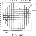
タスク625では、1または2以上の前処理予測マップが計算される。図8には、単純化された前処理予測マップ800を示すが、このマップは、複数のチップ/ダイ810と、番号付けされた前述の12の測定サイト830(1-12)と、ノッチ位置を示す参照側840とを有する。ある実施例では、曲線フィッティング手順が実施され、ウェハ上の未測定のサイトのデータが計算される。別の実施例では、予測マップは、表面予測技術、表面フィッティング技術、あるいは数学的技術を用いて定められる。
In
ある実施例では、第6行目からの測定データを用いて、第1の前処理式が計算され(測定サイト2、3、11)、この第1の前処理式を使用および/または修正して、チップ/ダイの予測値が計算され(6-3、6-4、6-6、6-7、6-8、6-9)、第1の前処理式を使用および/または修正して、チップおよび/またはダイ(6-0、6-1、6-11、6-12)の予測値が外挿される。あるいは、他の測定サイトを使用して、第1の前処理式が計算されても良い。
In one embodiment, the measurement data from the sixth line is used to calculate a first pre- processing equation (
第1の前処理式および/または修正版を使用して、第5行第7列目のチップ/ダイ値が計算/予測される。第1の前処理式は、必要な場合、5行目(測定サイト9)および7行目(測定サイト8)の測定データがフィッティングするように修正される。第1の前処理式が正確に決定および/または修正できないときは、エラー状況が示される。また、エラー状況は、1または2以上の測定値および/または計算/予測値が、ウェハに対して得られる均一性の限界を超えるときにも示される。 Using the first pre- processing equation and / or a modified version, the chip / die value in the fifth row and seventh column is calculated / predicted. The first pre-processing equation, if necessary, measurement data on the fifth line (measurement sites 9) and seventh row (measurement sites 8) is modified to fit. An error condition is indicated when the first pre- processing equation cannot be accurately determined and / or modified. An error condition is also indicated when one or more measured and / or calculated / predicted values exceed the uniformity limits available for the wafer.
また、第1の前処理式および/または修正版を使用して、ウェハ上の残りのサイトの値が計算/予測される。ある実施例では、第1の前処理式および/または修正版を用いて、第1の前処理予測マップの全体が計算される。1または2以上の計算値および/または予測値がウェハに対して得られる均一性の限界を超える場合、エラー状況が示される。あるいは、第1の前処理式および/または修正版を用いて、ウェハのある位置の値が計算/予測される。例えば、この部分は、1または2以上の象限を含んでも良い。 The first pre- processing equation and / or a modified version is also used to calculate / predict values for the remaining sites on the wafer. In some embodiments, using a first pre-processing equation and / or a modified version, the entire first pre-processing prediction map can be calculated. An error condition is indicated if one or more of the calculated and / or predicted values exceed the uniformity limits available for the wafer. Alternatively, the value of a certain position of the wafer is calculated / predicted using the first pre- processing equation and / or a modified version. For example, this portion may include one or more quadrants.
また、第7番目の列(測定サイト7、8、9、10)からの測定データを用いて、第2の前処理式が定められ、第2の前処理式を使用および/または修正して、チップ/ダイ(3-7、4-7、6-7、8-7、9-7、10-7)の予測値が計算され、第2の前処理式を使用および/または修正して、チップ/ダイの予測値が外挿される(0-7、1-7、12-7)。あるいは、他の測定サイトを使用して、第2の前処理式が決定される。
In addition, using the measurement data from the 7th column (
第2の前処理式および/または修正版を使用して、第5列と第6列のチップ/ダイの値が計算/予測される。第2の前処理式は、必要な場合、修正され、第6列(測定サイト5、6)と第5列(測定サイト4、3)の測定データについて、より良いフィッティングが得られる。第2の前処理式が正確に決定および/または修正できないときは、エラー状況が示される。また、エラー状況は、1または2以上の測定値および/または計算値/予測値が、ウェハに対して得られる均一性の限界を超える場合にも示される。
Using the second pre- processing equation and / or a modified version, the chip / die values in the fifth and sixth columns are calculated / predicted. The second pre- processing equation is modified if necessary to obtain a better fitting for the measurement data in the sixth column (
また、第2の前処理式および/または修正版を使用して、ウェハ上の残りのサイトの値を計算/予測しても良い。ある実施例では、第2の前処理式および/または修正版を用いて、第2の前処理マップ全体が計算される。1または2以上の計算値および/または予測値がウェハに対して得られる均一性の限界を外れる場合、エラー状況が示される。あるいは、第2の前処理式および/または修正版を用いて、ウェハのある部分の値が計算/予測される。例えば、この部分は、1または2以上の象限を含んでも良い。 The second pre- processing equation and / or a modified version may also be used to calculate / predict values for the remaining sites on the wafer. In some embodiments, using the second pre-processing equation and / or a modified version, the entire second pretreatment map can be calculated. An error condition is indicated if one or more of the calculated and / or predicted values are outside the uniformity limits available for the wafer. Alternatively, the value of a portion of the wafer is calculated / predicted using the second pre- processing equation and / or a modified version. For example, this portion may include one or more quadrants.
あるいは、第1の前処理式のみを使用して、第1の前処理マップが計算され、および/または第2の前処理式のみを使用して、第2の前処理マップが計算される。例えば、この手順を使用することにより、実質的に均一なプロセスのための処理時間が低減される。 Alternatively, using only the first pre-processing equation, the first pre-processing map is computed, and / or by using only the second pre-processing equation, the second pre-processing map can be calculated. For example, using this procedure reduces processing time for a substantially uniform process.
タスク630では、1または2以上の前処理信頼性マップが計算される。図9には、信頼性マップ920の単純化された一例を示すが、このマップは、複数のチップ/ダイ910と、(1-12)にラベル化された前述の12の測定サイト930と、ウェハのノッチ位置または基板の特定のサイトを示す参照サイド940とを有する。ある実施例では、前処理信頼性マップは、第1の前処理予測マップと第2の前処理予測マップの間の差異を用いて計算される。あるいは、前処理信頼性マップは、前処理予測マップと参照測定マップの間の差異を用いて計算される。
In
実施例に示したように、信頼性マップは、値「C1」、「C2」を用いて、異なる領域に分離され、異なる領域に、異なる値および/またはルールが構築される。例えば、2つの領域は、中央領域と端部領域の間の差異を示すために利用される。あるいは、異なる数の領域が使用されても良い。 As shown in the example, the reliability map is separated into different regions using the values “C1”, “C2”, and different values and / or rules are constructed in different regions. For example, the two regions are used to show the difference between the center region and the end region. Alternatively, a different number of areas may be used.
別の実施例では、前処理予測マップとウェハに対して得られる均一性限界の間の差異を用いて、前処理信頼性マップが計算される。例えば、予測マップ内の値が均一性限界に接近している場合、予測マップ内の値が均一性の限界に接近していない場合に比べて、信頼性値は、低くなる。 In another example, using the difference between the uniformity limit established for pre-processing prediction map and the wafer, the pre-processing confidence map is calculated. For example, when the value in the prediction map is approaching the uniformity limit, the reliability value is lower than when the value in the prediction map is not approaching the uniformity limit.
また、1または2以上の処理用の処理結果マップおよび/または信頼性マップを用いて、測定データ用の信頼性マップが計算されても良い。 Further, a reliability map for measurement data may be calculated using a processing result map and / or a reliability map for one or more processes.
タスク635では、前処理データに基づいて、いつ優先サイトを構築するかが質問される。信頼性マップ内の全ての領域の値が高い場合、新たな優先サイトを構築する必要はない。他の実施例では、予測マップ間の差異が小さく、および/または前処理予測マップと参照測定マップの間の差異が小さい場合、必ずしも新たな優先サイトを構築する必要はない。
At
また、信頼性マップ上の値が特定の処理に対して常に大きい場合、処理時間を低減するため、少数の測定サイトを使用し、新たな測定プランが構築されても良い。 If the value on the reliability map is always large for a specific process, a new measurement plan may be constructed using a small number of measurement sites in order to reduce the processing time.
信頼性マップの1または2以上の領域における1または2以上の値が低い場合、これらの領域に、1または2以上の新たな優先サイトが構築される。他の実施例では、予測マップ間の差異および/または前処理予測マップと参照測定マップの間の差異が大きい場合、1または2以上の新たな優先サイトが構築される。例えば、優先サイトは、ウェハ全体に対して、または特定の象限(Q1、Q2、Q3、またはQ4)のような、特定の領域に対して構築されても良い。 If one or more values in one or more regions of the reliability map are low, one or more new preferred sites are built in these regions. In other embodiments, one or more new preferred sites are built if the difference between prediction maps and / or the difference between the pre- processed prediction map and the reference measurement map is large. For example, the priority site may be built for the entire wafer or for a specific area, such as a specific quadrant (Q1, Q2, Q3, or Q4).
優先サイトが必要な場合、手順600は、タスク640に分岐し、優先サイトが不要な場合、手順600は、タスク645に分岐する。
If a preferred site is needed, the
タスク640では、1または2以上の優先サイトが構築される。図10には、新たな前処理測定マップ1020の単純化された図を示すが、このマップは、複数のチップ/ダイ1010と、新たな前処理測定サイト1035と、(1-12)にラベル化された前述の12の測定サイト1030と、ウェハ上のノッチ位置または基板の特定のサイトを示す参照サイド1040とを有する。あるいは、新たな前処理測定マップは、ウェハ上の異なる位置に、複数の優先サイトを有しても良い。ウェハのある領域の信頼性値が低い場合、その領域に、前処理測定サイトとして、1または2以上の優先サイトが構築される。例えば、第1の象限(Q1)における信頼性値が低い場合、優先サイトとしてチップ/ダイ(3-2)が同定され、測定ツールは、このサイトで測定を行うように指示される。
In
前処理信頼性マップは、計算された前処理予測値の信頼性用の指標となるとともに、測定された前処理データと、必要な要求の範囲内にある前処理予測データの指標となる。 Preprocessing confidence map, along with an indication of a reliability of the calculated pre-processing prediction value, a pretreatment data measured, is indicative of pre-processing prediction data that are within the scope of the necessary requirements.
新たな前処理優先サイトが必要な場合、新たな前処理測定レシピが形成され、新たなレシピを用いて、1または2以上の優先サイトで、測定ツールが追加の前処理測定を行うように指示される。 If a new pre- processing priority site is required, a new pre- processing measurement recipe is created and the new recipe is used to instruct the measurement tool to perform additional pre- processing measurements at one or more priority sites Is done.
ある実施例では、新たな前処理優先サイトは、過去に定めたサイトの組から選定される。例えば、構成および/または検査手順の間、40以上のサイトで測定が行われ、1または2以上のこれらのサイトが使用される。あるいは、新たな前処理優先サイトは、過去に定めたサイトの組から、選定されなくても良い。 In some embodiments, a new pretreatment prioritized site is selected from a set of sites determined in the past. For example, during configuration and / or inspection procedures, measurements are taken at 40 or more sites and one or more of these sites are used. Alternatively, a new pretreatment priority site, from a set of sites determined in the past may not be selected.
ウェハが測定ツール内にある間に前処理信頼性マップが計算されると、遅延が最小限に抑制されるようにして、新たに構築された優先サイトで、追加の測定が実施される。ウェハが測定ツールから排出された後に、信頼性マップが計算されると、ある遅延時間後に、新たなレシピが使用され、優先サイトで追加の測定が実施される。 Once the pre- process reliability map is calculated while the wafer is in the measurement tool, additional measurements are performed at the newly built priority site, with minimal delay. When the reliability map is calculated after the wafer is ejected from the measurement tool, after a certain delay time, a new recipe is used and additional measurements are performed at the priority site.
ある実施例では、優先サイトの測定データが形成されると、これは、前処理予測マップ内のデータと比較される。あるいは、優先サイトの測定データが形成されると、これは、保管され、後に、前処理予測マップ内のデータと比較されても良い。測定データがウェハにより構築された均一性の限界を外れると、エラー状況が示される。 In one embodiment, once the priority site measurement data is formed, it is compared to the data in the pre- processing prediction map. Alternatively, once the priority site measurement data is formed, it may be stored and later compared with the data in the pre- processing prediction map. An error condition is indicated when the measurement data falls outside the uniformity limits built by the wafer.
優先サイトの測定データが、特定の予測マップ内の値と接近している場合、この予測マップは、優先サイトの周囲の領域に利用される。例えば、1または2以上の優先サイトは、第1の象限内にあり、測定値が第1の前処理予測マップ内の値に近接している場合、第1の象限に、第1の前処理予測マップが使用される。 When the measurement data of the priority site is close to the value in the specific prediction map, this prediction map is used for the area around the priority site. For example, one or more prioritized sites are in the first quadrant, if the measured value is close to the value of the first pre-processing prediction map, the first quadrant, the first pre-processing A prediction map is used.
優先サイトの測定データが特定の予測マップ内の値に近接していない場合、新たな予測マップが形成され、優先サイトの周囲領域に、これが使用される。例えば、1または2以上の優先サイトが第1の象限内にあり、測定値が前処理予測マップ内の値とは近づいていない場合、新たな前処理予測マップが形成され、これが第1の象限に使用される。 If the priority site measurement data is not close to a value in a particular prediction map, a new prediction map is formed and used for the surrounding area of the priority site. For example, one or more prioritized sites is in the first quadrant, if the measured value is not approaching the value of the pre-processing prediction map, a new pre-processing prediction map is formed, this is the first quadrant Used for.
予測マップが変化すると、常時、新たな信頼性マップ、または信頼性マップの新たな部分が計算される。 Whenever the prediction map changes, a new reliability map or a new part of the reliability map is calculated.
タスク645では、信頼性マップが要求限界内にある場合、ウェハが処理される。ある実施例では、1または2以上のトリミングおよび/またはエッチングおよび/またはアッシング処理が実施され、ウェハ上にパターン化されたポリシリコン層が形成され、これらの処理は、図4に示すような手順で実施される。あるいは、異なる手順を実施しても良い。
In
ハードマスクトリミング手順の間、1または2以上の処理レシピ、および1または2以上の制御設定組(レシピパラメータ)が計算される。円形のウェハが処理される場合、処理レシピは、半径方向に変化が生じるように調整され、非円形のウェハが処理される場合、処理レシピは、横方向に変化が生じるように調整される。 During the hard mask trimming procedure, one or more processing recipes and one or more control setting sets (recipe parameters) are calculated. When a circular wafer is processed, the process recipe is adjusted to change in the radial direction, and when a non-circular wafer is processed, the process recipe is adjusted to change in the lateral direction.
ある実施例では、側方向のトリミング処理が実施され、ハードマスクフィーチャの寸法および/または形状が変化する。例えば、ハードマスク層は、TEOS材料を含んでも良い。処理システム100(図1)により、化学酸化反応(COR)処理が実施され、これにより、必要な寸法のハードマスクフィーチャが形成される。COR処理を実施するための方法およびシステムは、2003年12月17日に出願された、Tomoyasuらの「化学酸化除去用のシステムを作動する方法」という題目の同時係属中の米国特許出願第10/736,983号、および2003年11月12日に出願された、Hamelinらの「基板を処理する処理システムおよび方法」という題目の米国特許出願第10/705,201号に示されており、これらは、本願の参照として取り入れられている。 In some embodiments, a lateral trimming process is performed to change the size and / or shape of the hard mask feature . For example, the hard mask layer may include a TEOS material. The processing system 100 (FIG. 1) performs a chemical oxidation reaction (COR) process, which forms the hard mask features of the required dimensions. A method and system for performing COR processing is described in co-pending U.S. Patent Application No. 10 filed Dec. 17, 2003, entitled Tomoyasu et al., "Method of Operating a System for Chemical Oxidation Removal". No. 736,983 and US patent application Ser. No. 10 / 705,201 filed Nov. 12, 2003 entitled “Processing System and Method for Processing Substrates” by Hamelin et al. It has been incorporated as a reference.
次に、ハードマスクフィーチャを用いて、フィーチャがゲート材料層にエッチングされる。例えば、ゲート材料層は、ドープされたおよび/または未ドープのポリシリコン材料を含む。次に、清浄化処理が実施され、ハードマスク層の残留部分が除去される。例えば、アッシング処理および/または湿式清浄化処理が実施されても良い。次に、清浄化処理の実施後に、測定手順が実施される。あるいは、測定手順は、清浄化処理が実施される前に実施されても良い。 Next, using the hard mask features, features are etched into the gate material layer. For example, the gate material layer includes doped and / or undoped polysilicon material. Next, a cleaning process is performed to remove the remaining portion of the hard mask layer. For example, an ashing process and / or a wet cleaning process may be performed. Next, after the cleaning process is performed, a measurement procedure is performed. Alternatively, the measurement procedure may be performed before the cleaning process is performed.
図11には、本発明の実施例によるトリミング処理の一例を示す。示された実施例では、ハードマスクフィーチャ1005は、ウェハ1100上に示されており、上部層1130の残りの部分は、フィーチャの上部に示されている。あるいは、上部層1130はなくても良い。測定CD1110、測定側壁角度1135、対象CD1120、および対象側壁角度1125が示されている。所望の処理結果には、測定CD1110と対象CD1120の間の差異に相当するトリム量1140と、測定側壁角度1135と対象側壁角度1125の間の差異に相当する側壁角度とが含まれる。また、ターゲット値付近に形成された誤差があり、これらを用いて、GOFデータおよび/または信頼性データが定められる。(垂直エッチングとは反対の)トリムの場合、トリム処理は、構造の両表面で同時に行われる。このため、トリム量は、被覆ウェハに対する量の2倍となる。
FIG. 11 shows an example of trimming processing according to the embodiment of the present invention. In the illustrated embodiment, the hard mask feature 1005 is shown on the
ある実施例では、過去に計算された予測マップが、測定データマップとして使用される。あるいは、修正予測マップが使用されても良い。 In one embodiment, a previously calculated prediction map is used as the measurement data map. Alternatively, a modified prediction map may be used.
図12には、本発明による処理結果のマップの単純化された図を示す。図12には、単純化された処理結果マップ1220が示されており、これは、複数のチップ/ダイ1210と、(1-12)にラベル化された前述の12の測定サイト1230と、ウェハ上、または基板の特定の側のノッチ位置を示す参照側1240とを有する。ある実施例では、処理結果マップは、測定マップおよび/または処理マップを用いて定められる。あるいは、処理結果マップは、処理モデルを用いて定めても良い。
FIG. 12 shows a simplified diagram of a processing result map according to the present invention. FIG. 12 shows a simplified
図の実施例に示すように、処理結果マップは、「PR1」および「PR2」の値を用いて示された異なる領域に分離され、異なる領域に、異なる値および/またはルールが構築される。あるいは、異なる数の領域が使用されても良い。サイト「PR1」の第1の群は、これらに関連する第1組の処理結果を有し、サイト「PR2」の第2の群は、これらに関連する第2組の処理結果を有しても良い。2つの群は、本発明に必須ではなく、これらは、一例に過ぎない。代わりに、異なる数の群を使用しても良い。例えば、実質的に均一な組の処理結果が予測された場合、単一の群が使用され、2つの群を使用して、中央領域と端部領域の差異が示されても良い。また、2つの領域を用いて、計算処理を単純化し、またはこれらを使用して、中央領域と端部領域で生じる異なる処理結果および/または異なる測定結果を予測しても良い。 As shown in the illustrated example, the processing result map is separated into different regions indicated using the values of “PR1” and “PR2”, and different values and / or rules are constructed in different regions. Alternatively, a different number of areas may be used. The first group of site “PR1” has a first set of processing results related to them, and the second group of site “PR2” has a second set of processing results related to them. Also good. The two groups are not essential to the invention and these are only examples. Alternatively, a different number of groups may be used. For example, if a substantially uniform set of processing results is predicted, a single group may be used and the two groups may be used to indicate the difference between the central and end regions. Also, the two regions may be used to simplify the calculation process or be used to predict different processing results and / or different measurement results that occur in the central region and the end region.
エッチングおよび/またはトリミング処理が実施されると、1または2以上の処理結果マップが使用される。エッチング処理マップを用いて、垂直エッチングの量が特徴化され、側壁角度調整マップを用いて、側壁角度の変化量が特徴化され、マップに関連する誤差値を用いて、1または2以上の処理結果の許容量が定められる。トリム処理マップを用いて、水平方向のエッチング量が特徴化され、側壁角度調整マップを用いて、側壁角度の変化量が特徴化され、マップに関連する誤差値を用いて、1または2以上のデータ項目における許容量が定められる。また、処理信頼性マップを用いて、処理シーケンス内の1または2以上の処理に対するリスク因子が構築される。例えば、処理信頼性マップは、時間とともに変化し、チャンバ処理手順に応じて変化させても良い。 When an etching and / or trimming process is performed, one or more process result maps are used. Etch process maps are used to characterize the amount of vertical etching, sidewall angle adjustment maps are used to characterize the amount of change in sidewall angles, and error values associated with the map are used to process one or more processes. An acceptable amount of results is defined. The trim process map is used to characterize the amount of horizontal etching, the side wall angle adjustment map is used to characterize the amount of change in the side wall angle, and the error value associated with the map is used to calculate one or more. Tolerance in data items is defined. In addition, a risk factor for one or more processes in the process sequence is constructed using the process reliability map. For example, the process reliability map may change over time and may change depending on the chamber processing procedure.
トリミング手順が実施される際、制御方式は、1もしくは2以上のマップおよび/または予測式を有し、これらは、処理空間のモデル化のために形成される。ある実施例では、半径位置(rp)とともに、y(rp)=f(x,rp)のように変化する予測式が使用される。ある場合には、y(rp)は、ウェハ上の半径位置(r)での所望の処理結果と等しくなる。例えば、y(rp)は、「トリム量」[TA(rp)]のような所望の処理結果であっても良く、x(rp)は、y(rp)に関連する処理パラメータ(制御変数)と等しくても良い。処理空間では、1もしくは2以上の予測および/またはモデル化式が定められ、これは、処理ガス流速を処理空間の第1の部分におけるトリム量と関連付ける、多項式および多項式の係数を得る計算により得られる。例えば、N次の多項式が使用され、
あるいは、異なる多項式を形成し、異なる多項式の係数を求めることにより、逆数の式が求められても良い。この多項式により、逆数処理空間の異なる部分において、処理変数(ガス流速)が処理結果(トリム量)と関連付けられる。例えば、N次の多項式には、
制御器は、これらの種類の式および/またはモデルの項目のリストを計算し、制御器は、1または2以上の事項を操作する。事項は、制御器により定められ、処理内の少なくとも一つのステップが割り当てられる。あるいは、レシピパラメータマップが形成され、このマップ内で、各タームがパラメータ値に割り当てられる。 The controller calculates a list of items of these types of equations and / or models, and the controller operates on one or more items. Items are defined by the controller and assigned at least one step in the process. Alternatively, a recipe parameter map is formed, in which each term is assigned to a parameter value.
タスク650では、質問が実施され、後処理測定プロセスを実施するタイミングが定められる。処理が十分な場合、処理結果は、一定であり、各ウェハ毎に、後処理測定プロセスを行う必要はない。しかしながら、いくつかのウェハが、処理信頼性ウェハとして定められ、これらのウェハに対して、後処理測定プロセスが実施されても良い。処理が不十分で、処理結果が変化する場合、後処理測定プロセスが実施される。後処理測定プロセスが不要な場合、手順600は、タスク685に分岐し、後処理測定プロセスが必要な場合、手順600は、タスク655に分岐する。
At
ある実施例では、制御方式が実行され、これを用いて、後処理測定プロセスレシピが形成される。例えば、ウェハは、IMM140(図1)に送られ、ゲート材料にエッチング処理が実施されてから、パターン化されたウェハのフィーチャが測定される。例えば、TEMおよび/またはSEM測定が行われる。 In one embodiment, a control scheme is implemented and used to form a post-processing measurement process recipe. For example, the wafer is sent to the IMM 140 (FIG. 1) where the gate material is etched and the features of the patterned wafer are measured. For example, TEM and / or SEM measurements are performed.
図13Aには、複数のチップ/ダイ1310を有する円形ウェハ1300の後処理測定マップ1320の簡略化された図を示す。図13Bには、複数のチップ/ダイ1310を有する正方形形基板1350の簡略化された後処理測定マップ1320の図を示す。示された実施例では、125のチップ/ダイが示されているが、これは、本発明に必須ではない。代わりに、異なる数のチップ/ダイが使用されても良い。また、この形状は、一例のため示されており、本発明には必須ではない。例えば、チップ/ダイは、矩形状であっても良い。
FIG. 13A shows a simplified view of a
行および列は、ゼロから12まで示されている。また、12のチップ/ダイ1330は、ラベル化(1-12)され、これらのチップ/ダイを用いて、示された後処理測定プラン1320用の測定サイトの位置が定められる。あるいは、他の後処理測定プランおよび/または他の測定サイトが使用されても良い。
Rows and columns are shown from zero to twelve. Also, the twelve chips / dies 1330 are labeled (1-12) and these chips / dies are used to position the measurement site for the indicated
後処理測定プラン1320は、履歴データベースに保管されたデータに基づいて、半導体製造者により特定されても良い。例えば、半導体製造者は、SEM測定の際に、ウェハ上の多数の位置を選定し、統合測定ツールからの測定データを、SEMツールを用いて測定されたデータに関連付ける。他の製造者は、FIBデータを利用しても良い。
The
ある実施例では、後処理ウェハ上のフィーチャは、図13Aおよび13Bに示した12(1-12)の位置の1または2以上で測定される。例えば、後処理ウェハ上のフィーチャは、図4に示すようなものであっても良い。 In one embodiment, features on the post-process wafer are measured at one or more of the 12 (1-12) positions shown in FIGS. 13A and 13B. For example, the features on the post-process wafer may be as shown in FIG.
後処理測定マップは、1または2以上の良好フィッティング(GOF)マップ、1または2以上の格子厚さマップ、1または2以上の臨界寸法(CD)マップ、1または2以上のCDプロフィールマップ、1または2以上の材料断面領域マップ、1または2以上の溝断面積マップ、1または2以上の側壁角度マップ、1または2以上の差異幅マップ、またはこれらの組み合わせを有する。また、後処理データは、サイト結果データ、サイト数データ、CD測定フラグデータ、測定サイト数データ、座標xデータ、座標yデータ等を有しても良い。 Post-processing measurement maps include one or more good fitting (GOF) maps, one or more grid thickness maps, one or more critical dimension (CD) maps, one or more CD profile maps, 1 Or two or more material cross-sectional area maps, one or two or more groove cross-sectional area maps, one or two or more sidewall angle maps, one or two or more difference width maps, or a combination thereof. Further, the post-processing data may include site result data, site number data, CD measurement flag data, measurement site number data, coordinate x data, coordinate y data, and the like.
タスク660では、1または2以上の後処理予測マップが計算される。図14には、後処理予測マップ1420の単純化された図を示すが、このマップは、複数のチップ/ダイ1410と、前述のラベル化された12の測定サイト1430(1-12)と、ノッチ位置を示す参照サイド1440とを有する。ある実施例では、カーブフィッティング手順が実施され、非測定ウェハ上のサイトのデータが計算される。別の実施例では、予測マップは、表面予測、表面フィッティング技術、または他の数学技術を用いて定められる。
At
ある実施例では、第6行(測定サイト2、3、11)からの測定データを用いて、第1の後処理式が求められ、この第1の後処理式を使用および/または修正して、チップ/ダイの予測後処理測定データが計算され(6-3、6-4、6-6、6-7、6-8、6-9)、第1の後処理式を使用および/または修正して、チップ/ダイ用の予測後処理測定データの予測値が外挿される(6-0、6-1、6-11、6-12)。あるいは、他の測定サイトを使用して、第1の前処理式が定められる。
In one embodiment, the measurement data from the sixth line (
第1の後処理式および/または修正版を用いて、5行および7行のチップ/ダイの後処理値が計算/予測される。第1の後処理式は、必要な場合、修正して、5行(測定サイト9)と7行(測定サイト8)において、後処理測定データをフィッティングしても良い。第1の後処理式が適正に定まらず、および/または修正できないときには、エラー状況が示される。また、1または2以上の測定値および/または計算/予測値が、ウェハに対して得られる均一性限界から外れる場合、エラー状況が示される。 Using the first post-processing equation and / or a modified version, post-processing values for 5 rows and 7 rows of chips / dies are calculated / predicted. If necessary, the first post-processing equation may be modified to fit the post-processing measurement data on line 5 (measurement site 9) and line 7 (measurement site 8). An error condition is indicated when the first post-processing equation is not properly defined and / or cannot be corrected. An error condition is also indicated if one or more measured and / or calculated / predicted values deviate from the uniformity limits obtained for the wafer.
また、第1の後処理式および/または修正版を使用して、ウェハ上の残りのサイトの値が計算/予測される。ある実施例では、第1の後処理式および/または修正版を使用して、第1の後処理予測マップ全体が計算される。1または2以上の計算値および/または予測値が、ウェハに対して得られる均一性限界を超える場合、エラー状況が示される。あるいは、第1の後処理式および/または修正版を用いて、ウェハのある部分の値が計算/予測される。例えば、この部分は、1または2以上の象限を含んでも良い。 The first post-processing equation and / or modified version is also used to calculate / predict values for the remaining sites on the wafer. In one embodiment, the entire first post-processing prediction map is calculated using the first post-processing equation and / or a modified version. If one or more calculated and / or predicted values exceed the uniformity limits obtained for the wafer, an error condition is indicated. Alternatively, the value of a portion of the wafer is calculated / predicted using the first post-processing equation and / or a modified version. For example, this portion may include one or more quadrants.
また、7列(測定サイト7、8、9、10)からの後処理測定データを用いて、第2の後処理式が求められても良く、この第2の後処理式を使用および/または修正して、チップ/ダイ用(3-7、4-7、6-7、8-7、9-7、10-7)の実施される後処理測定データが計算され、第2の後処理式を使用および/または修正して、チップ/ダイ(0-7、1-7、12-7)用の予測後処理測定データの値が外挿される。あるいは、他の測定サイトを使用して、第2の後処理式を定めても良い。
Alternatively, a second post-processing equation may be determined using post-processing measurement data from seven columns (
第2の後処理式および/または修正版を用いて、5列と6列のチップ/ダイの値を計算/予測しても良い。第2の後処理式は、必要な場合、修正され、これにより、6列(測定サイト5、6)と5列(測定サイト4、3)のより良いフィッティングが可能となる。第2の後処理式が適正に定まらずおよび/または修正されない場合、エラー状況が示される。また、1または2以上の測定値および/または計算/予測値が、ウェハに対して得られる均一性を外れる場合、エラー状況が示される。
The second post-processing equation and / or a modified version may be used to calculate / predict values for the 5th and 6th rows of chips / dies. The second post-processing equation is modified, if necessary, to allow better fitting of 6 rows (
また、第2の後処理式および/または修正版を使用して、ウェハ上の残りのサイトの値が計算/予測される。ある実施例では、第2の後処理式および/または修正版を用いて、第2の後処理予測マップ全体が計算される。計算および/または予測された値の1または2以上が、ウェハに対して得られる均一性限界を外れる場合、エラー状況が示される。あるいは、第2の後処理式および/または修正版を使用して、ウェハのある部分の値を計算/予測しても良い。例えば、この部分は、1または2以上の象限を有する。 The second post-processing equation and / or a modified version is also used to calculate / predict values for the remaining sites on the wafer. In one embodiment, the entire second post-processing prediction map is calculated using the second post-processing equation and / or a modified version. An error condition is indicated if one or more of the calculated and / or predicted values are outside the uniformity limits obtained for the wafer. Alternatively, a second post-processing equation and / or a modified version may be used to calculate / predict values for a portion of the wafer. For example, this part has one or more quadrants.
あるいは、第1の前処理式のみを用いて、第1の後処理予測マップが計算され、第2の後処理式のみを用いて、第2の前処理マップが計算される。例えば、このような手順を使用した場合、実質的に均一な処理のための処理時間が抑制される。 Alternatively, the first post-processing prediction map is calculated using only the first pre- processing formula, and the second pre- processing map is calculated using only the second post-processing formula. For example, when such a procedure is used, the processing time for substantially uniform processing is suppressed.
タスク665では、1または2以上の後処理信頼性マップが計算される。図15には、後処理信頼性マップ1520の単純化された図を示すが、このマップは、複数のチップ/ダイ1510と、ラベル化(1-12)された前述の12の測定サイト1530と、ノッチ位置を示す参照側1540とを有する。ある実施例では、第1の後処理予測マップと第2の後処理予測マップの間の差異を用いて、後処理信頼性マップが計算される。あるいは、後処理予測マップと参照測定マップの間の差異を用いて、後処理信頼性マップが計算されても良い。
In
図の実施例に示すように、信頼性マップは、「C1」および「C2」で示すような異なる領域に分離され、異なる領域に、異なる値および/またはルールが構築されても良い。例えば、2つの領域を用いて、中央領域と端部領域の間の差異が示されても良い。あるいは、異なる数の領域が使用されても良い。 As shown in the illustrated example, the reliability map may be separated into different regions as indicated by “C1” and “C2”, and different values and / or rules may be constructed in different regions. For example, two regions may be used to indicate the difference between the central region and the end region. Alternatively, a different number of areas may be used.
別の実施例では、後処理予測マップと、ウェハに対して得られる均一性限界の差を用いて、後処理信頼性マップが計算される。例えば、予測マップ内の値が均一性限界と近い場合、予測マップの値が均一性限界に近くない場合に比べて、信頼性値は、小さくなる。 In another embodiment, a post-process reliability map is calculated using the post-process prediction map and the difference in uniformity limits obtained for the wafer. For example, when the value in the prediction map is close to the uniformity limit, the reliability value is smaller than when the value in the prediction map is not close to the uniformity limit.
ある実施例では、第1の種類の後処理信頼性データにより、測定データに対する信頼性の予測値が提供され、換言すれば、予測された測定データが正しいかどうかがを示す予測値が提供される。ウェハ全体の測定には、時間がかかるため、少量の測定サイトが使用され、信頼性因子が構築され、これにより、予測された測定データが、ウェハのより多くのサイトまたはより多くの部分を用いて、測定を行った場合に得られるデータを正確に表していることが確認される。第2の種類の後処理信頼性マップにより、トリミング処理の信頼性の予測が提供される。処理された後に、ウェハ全体を測定した場合、時間がかかり、半導体製造者は、処理が正確に実施されたかを確認することを望むため、実際の測定データおよび/または予測測定データが、予測ターゲット値と比較され、これらの数が特定の限界を有する場合、半導体製造者は、ウェハ全体が測定されていなくても、処理が正確に実施されたと推定することができる。 In one embodiment, the first type of post-processing reliability data provides a predicted value of reliability for the measured data, in other words, a predicted value indicating whether the predicted measured data is correct. The Since the entire wafer measurement takes time, a small number of measurement sites are used and a reliability factor is built, so that the predicted measurement data uses more sites or more parts of the wafer. Thus, it is confirmed that the data obtained when the measurement is performed is accurately represented. A second type of post-processing reliability map provides a prediction of the reliability of the trimming process. When the entire wafer is measured after processing, it takes time and the semiconductor manufacturer wants to verify that the process has been performed correctly, so the actual measurement data and / or the predicted measurement data is When compared to the values and these numbers have certain limits, the semiconductor manufacturer can deduce that the process has been performed correctly even if the entire wafer has not been measured.
タスク670では、質問が実施され、後処理データに基づいて、優先サイトを構築するタイミングが定められる。後処理信頼性マップの全ての領域において、値が大きい場合、必ずしも新たな優先サイトを構築する必要はない。他の実施例では、予測マップ間の差異が小さく、および/または後処理予測マップと参照測定マップの間の差異が小さい場合、必ずしも優先サイトを構築する必要はない。
In
また、特定の処理において、後処理信頼性マップの値が常時大きい場合、新たな測定プランが構築され、これを用いて、少数の測定サイトが利用され、処理時間が低減される。 Further, in a specific process, when the value of the post-processing reliability map is always large, a new measurement plan is constructed, and using this, a small number of measurement sites are used, and the processing time is reduced.
後処理予測マップ内の1または2以上の領域において、1または2以上の値が小さい場合、これらの領域に、1または2以上の新たな優先サイトが構築される。他の実施例では、後処理予測マップ間の差異が大きく、および/または後処理予測マップと参照測定マップの間の差異が大きい場合、1または2以上の新たな優先サイトが構築が構築される。例えば、優先サイトは、ウェハ全体に対して構築されても良く、または特定の象限(Q1、Q2、Q3、Q4)のような特定の領域に構築されても良い。 When the value of 1 or 2 or more is small in 1 or 2 or more areas in the post-processing prediction map, 1 or 2 or more new priority sites are constructed in these areas. In other embodiments, if the difference between the post-processing prediction map is large and / or the difference between the post-processing prediction map and the reference measurement map is large, one or more new preferred sites are built. . For example, the priority site may be constructed for the entire wafer, or may be constructed in a specific area such as a specific quadrant (Q1, Q2, Q3, Q4).
後処理優先サイトが必要な場合、手順600は、タスク675に分岐し、後処理優先サイトが不要な場合、手順600は、タスク680に分岐する。
If a post-processing priority site is required, the
タスク675では、1または2以上の優先サイトが構築される。図16には、新たな後処理測定マップ1620の単純化された図を示すが、このマップは、複数のチップ/ダイ1610と、新たな後処理測定サイト1635と、ラベル化(1-12)された前述の12の測定サイト1630と、ウェハのノッチ位置または基板の特定サイドを示す参照サイド1640とを有する。あるいは、新たな後処理測定マップは、ウェハ上の異なる位置に、複数の優先サイトを有しても良い。ウェハの一つの領域の信頼性値が小さい場合、1または2以上の優先サイトは、後処理測定サイトとして、その領域に構築される。例えば、第1の象限(Q1)において、信頼性値が小さい場合、チップ/サイト(3-2)が優先サイトとして定められ、測定ツールは、このサイトで測定を実施するように指示される。
In
新たな後処理優先サイトが必要な場合、新たな後処理測定レシピが形成され、新たなレシピを用いて、1または2以上の優先サイトで、追加の後処理測定を実施するように測定ツールが指令を受ける。ウェハが測定ツールにある間に、後処理信頼性マップが計算されると、最小の遅延となるようにして、新たに構築された優先サイトで、追加の測定が実施される。ウェハが測定ツールから排出された後に、後処理信頼性マップが計算されると、後に、新たなレシピが使用され、ある遅延時間の後、優先サイトで、追加の測定が実施される。 If a new post-processing priority site is needed, a new post-processing measurement recipe is created and the measurement tool can use the new recipe to perform additional post-processing measurements at one or more priority sites. Receive a directive. When the post-process reliability map is calculated while the wafer is in the measurement tool, additional measurements are performed at the newly constructed priority site with minimal delay. When the post-process reliability map is calculated after the wafer is ejected from the measurement tool, a new recipe is later used and after a certain delay time, additional measurements are performed at the priority site.
ある実施例では、優先サイト用の測定データが形成されると、これは、後処理予測マップのデータと比較される。あるいは、優先サイト用の測定データが形成されると、これは、保管され、後に、後処理予測マップ内のデータと比較される。優先サイトの測定データがウェハの均一性要求により構築された限界を外れると、エラー状況が示される。 In one embodiment, once the measurement data for the preferred site is formed, it is compared to the post-processing prediction map data. Alternatively, once the measurement data for the priority site is formed, it is stored and later compared with the data in the post-processing prediction map. If the priority site measurement data falls outside the limits built by the wafer uniformity requirement, an error condition is indicated.
優先サイトの測定データが、特定の予測マップ内の値と接近している場合、優先サイトの周囲領域に、この予測マップが用いられる。例えば、1または2以上の優先サイトが第1の象限内にあり、測定値が第1の後処理予測マップ内の値と接近している場合、第1の象限に、第1の後処理予測マップが使用される。 When the measurement data of the priority site is close to the value in the specific prediction map, this prediction map is used in the surrounding area of the priority site. For example, if one or more priority sites are in the first quadrant and the measured value is close to the value in the first post-processing prediction map, the first post-processing prediction in the first quadrant A map is used.
優先サイトの測定データが、特定の予測マップ内の値と接近していない場合、新たな優先マップが形成され、優先サイトの周囲領域に、これが用いられる。例えば、1または2以上の優先サイトが第1の象限内にあり、測定値が前処理予測マップ内の値と接近していない場合、新たな前処理予測マップが形成され、第1の象限に、これが使用される。 If the measurement data of the priority site is not close to the value in the specific prediction map, a new priority map is formed and used for the surrounding area of the priority site. For example, if one or more priority sites are in the first quadrant and the measured value is not close to the value in the pre- processing prediction map, a new pre- processing prediction map is formed and the first quadrant , This is used.
後処理予測マップが変化すると、常時、新たな後処理信頼性マップ、または後処理信頼性マップの新たな部分が計算される。 Whenever the post-processing prediction map changes, a new post-processing reliability map or a new part of the post-processing reliability map is calculated.
測定ツール用に新たな後処理測定レシピが形成され、後に、この新たな測定レシピを用いて、1または2以上の優先サイトで測定を実施するように、測定ツールが指示される。例えば、新たな測定レシピを用いて、次のウェハまたはいくつかの他のウェハが測定される。あるいは、現在のウェハを測定ツール内に搬送して、新たな後処理測定レシピを使用して、このウェハの再測定を行っても良い。 A new post-processing measurement recipe is created for the measurement tool, and the measurement tool is later instructed to perform measurements at one or more preferred sites using this new measurement recipe. For example, a new measurement recipe is used to measure the next wafer or several other wafers. Alternatively, the current wafer may be transferred into the measurement tool and remeasured using a new post-processing measurement recipe.
後処理予測マップが変更されると、常時新たな後処理信頼性マップ、または後処理信頼性マップの新たな部分が計算される。また、平均後処理予測マップが計算されても良い。例えば、ウェハ全体、または特定の象限(Q1、Q2、Q3、Q4)のような特定の領域に対して、平均後処理予測マップが計算される。 When the post-processing prediction map is changed, a new post-processing reliability map or a new part of the post-processing reliability map is always calculated. An average post-processing prediction map may be calculated. For example, an average post-processing prediction map is calculated for a specific region, such as the entire wafer or a specific quadrant (Q1, Q2, Q3, Q4).
タスク680では、質問が行われ、別の後処理測定プロセスを実施するタイミングが決定される。処理が十分な場合、処理結果は、一定となり、後処理測定プロセスは不要となる。しかしながら、いくつかのウェハが、処理信頼性ウェハとして定められ、これらのウェハに対して後処理測定プロセスが実施されても良い。処理が不十分で、処理結果が変化する場合、後処理測定プロセスが実施される。別の後処理測定プロセスが実施されても良い。別の後処理測定プロセスが不要な場合、手順600は、タスク685に分岐し、後処理測定プロセスが必要な場合、手順600は、タスク655に分岐する。
At
ある実施例では、1または2以上の優先サイトが定められ、1または2以上の優先サイトで、後処理測定処理プロセスが実施される。 In some embodiments, one or more priority sites are defined and a post-processing measurement process is performed at one or more priority sites.
ある実施例では、過去に計算された予測マップが、測定データマップとして使用される。あるいは、修正された予測マップが使用されても良い。 In one embodiment, a previously calculated prediction map is used as the measurement data map. Alternatively, a modified prediction map may be used.
タスク685では、質問が実施され、ウェハに追加の処理が必要なタイミングが定められる。処理が実施されると、多数のウェハが、ロットまたはバッチで処理される。追加のウェハ処理が不要な場合、手順600は、タスク690に分岐し、追加のウェハ処理が必要な場合、手順600は、タスク610に分岐する。
In
手順600は、タスク690で完了する。
The
別の実施例では、BARC材料および/またはARC材料および/またはハードマスク材料として、調整エッチング抵抗ARC(TERA)材料が使用され、ゲート材料は、GaAs、SiGe、および歪みシリコンを含む。 In another embodiment, a tuned etch resistance ARC (TERA) material is used as the BARC material and / or ARC material and / or hard mask material, and the gate material includes GaAs, SiGe, and strained silicon.
図17A乃至17Cには、本発明の実施例による動的サンプリングを実施するための、異なる処理方法を示す。3種類の異なる方法で、ウェハ測定レシピ設定(測定のための可変レシピ調整)を計算するアプリケーションが使用される:第1の方法は、測定解析システム(Timbre(登録商標)PAS)を使用し、第2の方法は、ツール処理システム(Telius(登録商標)/Ingenio(登録商標))を使用し、第3の方法は、工場ホストを使用する。 17A-17C illustrate different processing methods for performing dynamic sampling according to embodiments of the present invention. Three different methods are used to calculate wafer measurement recipe settings (variable recipe adjustment for measurement): The first method uses a measurement analysis system (Timbre® PAS), The second method uses a tool processing system (Telius® / Ingenio®) and the third method uses a factory host.
図17Aに示された実施例では、測定解析システム内のPAS制御器により、1または2以上の動的サンプリングが実施される。1Aでは、ウェハ内容を有するレシピリストがIMに送信され、PJスタート命令が使用される。2Aでは、IMがウェハ内容をPAS制御器に送信し、これには、追加のウェハマップが含まれても良い。3Aでは、PAS制御器は、1または2以上の動的サンプリング(DS)アプリケーションが呼び出される。4Aでは、DSアプリケーションを用いて、ウェハのマップサイト位置調整が計算される。5Aでは、PAS制御器により、可変調整メッセージがIMに送信される。6Aでは、IMにより修正レシピを用いた測定が実施される。 In the example shown in FIG. 17A, one or more dynamic samplings are performed by a PAS controller in the measurement analysis system. In 1A, a recipe list with wafer contents is sent to IM and a PJ start command is used. In 2A, the IM sends the wafer contents to the PAS controller, which may include additional wafer maps. In 3A, the PAS controller is called by one or more dynamic sampling (DS) applications. In 4A, the DS map application is used to calculate the wafer map site alignment. In 5A, the PAS controller sends a variable adjustment message to IM. In 6A, measurement using a modified recipe is performed by IM.
図17Bに示した実施例では、アドバンス処理制御(APC)システム内の制御器により、1または2以上の動的サンプリングが実施される。1Bでは、ウェハ内容を含むレシピリストがIMに送信され、PJスタート命令が使用される。2Bでは、ツールにより、ウェハ内容がAPC制御器に送信され、これには、追加のウェハマップが含まれても良い。3Bでは、APC制御器が1または2以上のDSアプリケーションが呼び出される。4Bでは、DSアプリケーションを用いて、ウェハマップサイト位置調整が計算される。5Bでは、ツール制御器により、APC制御器からの可変調整メッセージが受信される。6Bでは、ツール制御器により、可変調整メッセージがIMに送信される。7Bでは、IMにより、修正レシピを用いて、測定が行われる。 In the embodiment shown in FIG. 17B, one or more dynamic samplings are performed by a controller in an advanced processing control (APC) system. In 1B, a recipe list containing the wafer contents is sent to IM and a PJ start command is used. In 2B, the tool sends the wafer content to the APC controller, which may include additional wafer maps. In 3B, DS applications with one or more APC controllers are called. In 4B, the wafer map site alignment is calculated using the DS application. In 5B, the tool controller receives a variable adjustment message from the APC controller. In 6B, the tool controller sends a variable adjustment message to the IM. In 7B, measurement is performed by IM using a modified recipe.
図17Cに示した実施例では、ホストシステム内の制御器により、1または2以上の動的サンプリングのアプリケーションが実施される。1Cでは、IMに、ウェハ内容を含むレシピリストが送信される。1Cでは、ウェハ内容を含むレシピリストがIMに送信され、PJ開始命令が使用される。2Cでは、ツールにより、ウェハ内容がホスト制御器に送信され、これには追加のウェハマップが含まれても良い。3Cでは、ホスト制御器により、1または2以上のDSアプリケーションが呼び出される。4Cでは、DSアプリケーションを用いて、ウェハマップサイト位置調整が計算される。5Cでは、ホスト制御器により、可変調整メッセージがIMに送信される。7Cでは、IMにより、修正レシピを用いた測定が実施される。 In the embodiment shown in FIG. 17C, one or more dynamic sampling applications are implemented by a controller in the host system. In 1C, a recipe list including wafer contents is transmitted to IM. In 1C, a recipe list containing the wafer contents is sent to IM and a PJ start command is used. In 2C, the tool sends the wafer contents to the host controller, which may include additional wafer maps. In 3C, one or more DS applications are invoked by the host controller. In 4C, wafer map site alignment is calculated using the DS application. In 5C, the host controller sends a variable adjustment message to the IM. In 7C, measurement using a modified recipe is performed by IM.
図1を再度参照すると、制御器120は、導入材料の測定マップ(入力状態)と、処理結果マップ(所望の状態)との間の差異を使用して、処理パラメータ組を予測し、選定し、または計算し、入力状態から、所望の状態にウェハの状態を変化させるための所望の結果が得られる。例えば、この処理パラメータの予測組は、レシピの第1の予測であり、これを用いて、均一な処理が提供される。また、測定マップおよび/または処理結果マップがMES130から得られ、これを用いて、第1の予測を更新しても良い。
Referring back to FIG. 1, the
制御器120は、1または2以上の入力状態マップに基づいて、1または2以上の処理モジュール特性マップに基づいて、ならびに1または2以上の処理モジュールに基づいて、ウェハの予測状態マップを計算する。例えば、所持時間とともに、トリム速度マップが使用され、予測とリム量マップが計算される。あるいは、処理時間とともに、エッチング速度マップが使用され、エッチング深さマップが計算され、処理時間とともに、成膜速度マップが使用され、成膜厚さマップが計算される。
The
制御器120は、後処理測定マップおよび/またはデータに使用され、第1組の処理偏差が計算される。この処理偏差の計算組は、1または2以上の所望の処理結果マップ、ならびに1または2以上の後処理測定マップから定められた、実際の処理結果マップに基づいて定められる。ある場合には、制御器120は、必要なマップを取得し、制御器120は、1または2以上のマップを用いて、所望の状態と実際の状態の間のこの差異を定める。この方法では、1または2以上の測定された実際の処理結果マップが、1または2以上の所望の処理結果マップと比較され、処理レシピに対する関係が定められる。例えば、「結果」マップは、上部CDマップ、底部CDマップ、側壁角度マップを有し、トリム処理、BARCオープンエッチング処理、および/または分離/ネスト化エッチング処理用の処理レシピとの関係が形成される。
別の場合には、制御器120は、ウェハの1または2以上の予測状態マップと、1または2以上の出力状態マップとを取得し、制御器120により、予測状態マップと出力状態マップの間の差異が定められる。この方法では、測定された実際の処理結果マップが、予測処理結果マップと比較され、1もしくは2以上の処理モデルおよび/またはマップとの関係が求められる。例えば、「結果」マップは、上部CDマップ、底部CDマップ、側壁角度マップを有し、トリム処理、BARC/ARCオープンエッチング、および/または分離/ネスト化エッチング処理用の処理モデルに対する関係が形成される。
In another case, the
マップは、フィードバックデータを用いて更新され、このフィードバックデータは、モニター用、試験用および/または製品ウェハを稼働し、処理設定を変化させ、結果を観察し、1または2以上の異なるマップを更新することにより形成される。例えば、マップの更新は、各N処理時間毎に行われ、モニタ用ウェハの特徴の測定の前および後に、行われる。異なる差動領域を調べる時間の設定を変更することにより、時間に対して作動空間全体が有効となり、またはいくつかのモニタ用ウェハを、異なるレシピ設定で同時に稼働することが可能になる。マップの更新は、制御器120内で、処理ツールで、または工場で行われ、工場により、モニタ用ウェハとマップ更新を制御および/または管理することが可能になる。
The map is updated with feedback data that runs monitor, test and / or product wafers, changes process settings, observes results, and updates one or more different maps It is formed by doing. For example, the map is updated every N processing times, and before and after measurement of the characteristics of the monitor wafer. By changing the time settings for examining different differential regions, the entire working space is enabled with respect to time, or several monitoring wafers can be operated simultaneously with different recipe settings. Map updates are performed within the
制御器120により、処理手順の1または2以上の時点で、マップが更新される。ある場合には、制御器120は、フィードフォワード情報、モデル化情報、およびフィードバック情報を使用し、現在のウェハに使用される前、次のウェハに使用される前、または次のロットに使用される前に、1または2以上の現在使用中のマップを変更するかどうかが定められる。
The
処理の信頼性因子が定められる際、必要な処理結果マップが使用される。必要な処理結果マップは、所望の処理結果マップと実際の測定データマップの間の差異を有する。測定データに対して、対象データのような、所望の処理結果データが計算される。例えば、所望の処理結果マップは、所望の溝領域マップ、所望の材料厚さマップ、所望の側壁角度マップ、所望の格子厚さマップ、所望のフィーチャプロファイルマップ、所望のトリム量マップ、所望の差分深さマップ、所望の均一性マップ、および所望の差分幅マップの少なくとも一つを有する。 When the process reliability factor is determined, the required process result map is used. The required processing result map has a difference between the desired processing result map and the actual measurement data map. For the measurement data, desired processing result data such as target data is calculated. For example, the desired processing result map may be a desired groove region map, a desired material thickness map, a desired sidewall angle map, a desired grid thickness map, a desired feature profile map, a desired trim amount map, a desired difference. At least one of a depth map, a desired uniformity map, and a desired difference width map.
マップ化を実施する場合、マップ源が重要となり、これは、予め定められる。例えば、マップは、外部発生または内部発生のいずれであっても良い。外部発生マップは、MES130により提供される。内部発生マップは、GUIからの計算値および/または入力を用いて、形成される。また、外部発生マップまたは内部発生マップを使用するタイミングを定める際に使用され得る、ビジネスルールが提供される。マップは、これらが使用される前に、評価され、あるいは予め適合される。
When implementing mapping, the map source is important and this is predetermined. For example, the map can be either externally generated or internally generated. The external generation map is provided by the
以上、本発明のある実施例のみについて詳細に示したが、本発明の新たな示唆および利点から実質的に逸脱しないで、実施例に多くの修正が可能であることは、当業者には容易に理解できる。従って、そのような全ての修正は、本発明の範囲に属するものである。 Although only certain embodiments of the present invention have been described in detail above, it will be readily apparent to those skilled in the art that many modifications can be made to the embodiments without substantially departing from the new suggestions and advantages of the present invention. Can understand. Accordingly, all such modifications are within the scope of the present invention.
すなわち、本文の記載は、本発明を限定するものではなく、本発明の構成、動作、および挙動は、所与のレベルで、実施例の修正および変更が可能であることを示すために記載されている。従って、前述の記載は、本発明を限定することを決して意味するものではなく、本発明の範囲は、特許請求の範囲により定められる。 In other words, the description of the text is not intended to limit the present invention, and the configuration, operation, and behavior of the present invention are described to show that the embodiments can be modified and changed at a given level. ing. Therefore, the foregoing description is in no way meant to limit the invention, but the scope of the invention is defined by the claims.
Claims (7)
ウェハを受容するステップであって、前記ウェハは、複数のダイを有し、各ダイは、少なくとも一つの他の層の上部に、パターン化されたハードマスク層を有するステップと、
前記ウェハに対する測定手法データ(metrology data)を定めるステップであって、前記測定手法データは、前記ウェハ上の少なくとも一つのハードマスクフィーチャの臨界寸法(CD)データ、および前記少なくとも一つの他の層用のデータを含み、前記測定手法データは、第1組の複数のダイ上の測定サイトから、履歴データ、測定データ(measured data)またはこれらの組み合わせを用いて定められ、残りの複数のダイは、未測定サイトを有する第2組の複数のダイを形成する、ステップと、
前記測定サイトから、前記測定手法データを用いて、前記ウェハの前処理測定マップを形成するステップと、
前記前処理測定マップの第1の方向に配置された2以上の前記測定サイトから、前記測定手法データを用いて、第1の前処理式を定めるステップと、
前記前処理測定マップの第2の方向に配置された2以上の前記測定サイトから、前記測定手法データを用いて、第2の前処理式を定めるステップと、
前記第1の前処理式を用いて、前記ウェハの第1の前処理予測マップを計算するステップであって、前記第1の前処理予測マップは、前記第2組の複数のダイ上の1または2以上の前記未測定サイトの第1組の予測測定値を有する、ステップと、
前記第2の前処理式を用いて、前記ウェハの第2の前処理予測マップを計算するステップであって、前記第2の前処理予測マップは、前記第2組の複数のダイ上の1または2以上の前記未測定サイトの第2組の予測測定値を有する、ステップと、
前記ウェハの前処理信頼性マップを計算するステップであって、前記前処理信頼性マップは、前記第1の前処理予測マップおよび前記第2の前処理予測マップにおける前記第1および第2組の予測測定値の間の差値に基づいた、前記第2組の複数のダイ用の信頼性データを有し、大きな差値は、前記ウェハの処理の均一性を得るための低い信頼性を表し、小さな差値は、前記ウェハの処理の均一性を得るための高い信頼性を表すステップと、
前記第2組の複数のダイにおける1または2以上のダイの前記信頼性データが、前記ウェハの処理の均一性を得るための低い信頼性を示した場合、低い信頼性を示す前記1または2以上のダイを含む、前記ウェハの1または2以上の領域において、1または2以上の優先測定サイトを定めるステップと、
前記1または2以上の優先測定サイトを含む新たな測定レシピを用いて、前記ウェハに対する新たな測定手法データを取得するステップと、
を有する方法。A method of processing a wafer comprising:
Receiving a wafer, the wafer having a plurality of dies, each die having a patterned hard mask layer on top of at least one other layer;
Determining metrology data for the wafer, wherein the metrology data is for critical dimension (CD) data of at least one hard mask feature on the wafer, and for the at least one other layer The measurement technique data is determined from the measurement sites on the first set of multiple dies using historical data, measured data, or a combination thereof , and the remaining multiple dies are: Forming a second set of dies having unmeasured sites; and
Using the measurement technique data from the measurement site to form a pre- process measurement map of the wafer;
From the two or more measurement sites arranged in the first direction of the preprocessing measurement map, using the measurement technique data, determining a first preprocessing equation;
From the two or more measurement sites arranged in the second direction of the preprocessing measurement map, using the measurement technique data, determining a second preprocessing formula,
Calculating a first pre- processing prediction map for the wafer using the first pre-processing equation , wherein the first pre-processing prediction map is 1 on the second set of dies; or two or more of the having a first set of predicted measurements unmeasured site, the steps,
Calculating a second pre- processing prediction map for the wafer using the second pre-processing equation , wherein the second pre- processing prediction map is 1 on the plurality of dies in the second set; or two or more of the having a second set of predicted measurements unmeasured site, the steps,
Calculating a pre- processing reliability map of the wafer, wherein the pre- processing reliability map is a set of the first and second sets in the first pre-processing prediction map and the second pre-processing prediction map. Having reliability data for the second set of multiple dies based on the difference value between predicted measurements, with large difference values representing low reliability to obtain processing uniformity of the wafer The small difference value represents a high reliability for obtaining uniformity of processing of the wafer ;
If the reliability data of one or more dies in the second set of dies indicates low reliability to obtain processing uniformity of the wafer, the 1 or 2 indicating low reliability Including one or more prioritized measurement sites in one or more regions of the wafer, including the above dies ;
Using a new measurement recipe including the one or more priority measurement sites, obtaining new measurement technique data for the wafer;
Having a method.
前記第2組のダイの前記信頼性データが、処理の均一性を得るため高い信頼性を示した場合、前記ウェハの制御設定値を計算するステップと、
前記計算された制御設定値を用いて、前記ウェハを処理するステップと、
を有することを特徴とする請求項1に記載の方法。further,
If the reliability data of the second set of dies exhibits high reliability to obtain process uniformity , calculating a control setpoint for the wafer;
Processing the wafer using the calculated control settings;
The method of claim 1, comprising:
前記ウェハ上の少なくとも一つのハードマスクフィーチャの寸法を用いて、トリム値を定めるステップと、
化学酸化除去(OCR)処理を用いて、トリム化されたマスク層を形成するステップと、
を有することを特徴とする請求項2に記載の方法。further,
Determining a trim value using a dimension of at least one hard mask feature on the wafer;
Forming a trimmed mask layer using a chemical oxidative removal (OCR) process;
The method of claim 2, comprising:
前記第1組の複数のダイ上の前記測定サイトからの前記測定手法データ、および前記1または2以上の優先測定サイトからの新たな測定手法データを用いて、新たな前処理測定マップを形成するステップと、
前記ウェハの新たな前処理予測マップを計算するステップであって、前記新たな前処理予測マップは、前記1または2以上の優先測定サイトの周囲の領域において、前記第2組の複数のダイ上の1または2以上の前記未測定サイトの新たな組の予測測定データを含むステップと、
前記ウェハの新たな信頼性マップを計算するステップであって、前記新たな信頼性マップは、前記第1および/または第2の前処理予測マップの間の差値、および前記新たな前処理予測マップに基づく、前記第2組の複数のダイの新たな信頼性データを含むステップと、
前記1または2以上の優先測定サイトの前記新たな測定手法データが、ウェハの均一性仕様によって構築された限界範囲にない場合、エラー状況が形成されるステップと、
前記第2組のダイの前記新たな信頼性データが、処理の均一性を得るための高い信頼性を示す場合、前記ウェハが処理されるステップと、
を有することを特徴とする請求項1に記載の方法。further,
Form a new pre- processing measurement map using the measurement technique data from the measurement sites on the first set of dies and the new measurement technique data from the one or more priority measurement sites Steps,
And calculating a new pre-processing prediction map of the wafer, the new pre-processing prediction map around the region of the one or more prioritized measuring site, the second set of the plurality of dies Including a new set of predicted measurement data for one or more of said unmeasured sites ;
Calculating a new reliability map of the wafer, wherein the new reliability map is a difference value between the first and / or second pre-processing prediction map, and the new pre-processing prediction. Including new reliability data of the second set of dies based on a map ;
An error situation is formed if the new measurement technique data of the one or more preferred measurement sites is not within a limit range established by a wafer uniformity specification ;
If the new reliability data of the second set of dies indicates high reliability to obtain process uniformity , the wafer is processed; and
The method of claim 1, comprising:
後処理測定手法データが必要な場合、測定モジュール内で、前記処理されたウェハを測定するステップであって、前記第1組の複数のダイ上の前記測定サイトから、後処理測定手法データが生じるステップ、
を有することを特徴とする請求項2に記載の方法。further,
If post-processing measurement technique data is required, measuring the processed wafer in a measurement module, wherein post-processing measurement technique data is generated from the measurement sites on the first set of dies Step,
The method of claim 2, comprising:
前記処理されたウェハの前記後処理測定手法データを用いて、後処理測定マップを形成するステップと、
前記後処理測定マップの第1の方向に配置された2以上の前記測定サイトから、前記後処理測定手法データを用いて、第1の後処理式を定めるステップと、
前記後処理測定マップの第2の方向に配置された2以上の前記測定サイトから、前記後処理測定手法データを用いて、第2の後処理式を定めるステップと、
前記第1の後処理式を用いて、前記処理されたウェハの第1の後処理予測マップを計算するステップであって、前記第1の後処理予測マップは、前記第2組の複数のダイ上の1または2以上の前記未測定サイト用の、第1組の予測後処理測定値を含むステップと、
前記第2の後処理式を用いて、前記処理されたウェハの第2の後処理予測マップを計算するステップであって、前記第2の後処理予測マップは、前記第2組の複数のダイ上の前記1または2以上の前記未測定サイト用の、第2組の予測後処理測定値を含むステップと、
前記処理されたウェハの後処理信頼性マップを計算するステップであって、前記後処理信頼性マップは、前記第1の後処理予測マップと前記第2組の後処理予測マップにおける、前記第1および第2組の予測後処理測定値の間の差値に基づく、前記処理されたウェハ上の前記第2組の複数のダイ用の後処理信頼性データを含み、高い差値は、前記処理されたウェハの処理の均一性に低い信頼性が得られることを示し、低い差値は、前記処理されたウェハの処理の均一性に高い信頼性が得られることを示すステップと、
前記第2組の複数のダイにおける、1または2以上のダイの前記後処理信頼性データが、前記処理されたウェハの処理の均一性において低い信頼性が得られることを示す場合、低い信頼性を示す前記1または2以上のダイを含む前記ウェハの1または2以上の領域に、1または2以上の優先後処理測定サイトが構築されるステップと、
前記1または2以上の優先後処理測定サイトを含む新たな測定レシピを用いて、前記ウェハの新たな後処理測定手法データが取得されるステップと、
を有することを特徴とする請求項5に記載の方法。further,
Using the post-processing measurement technique data of the processed wafer to form a post-processing measurement map;
From the two or more measurement sites arranged in the first direction of the post-processing measurement map, using the post-processing measurement technique data, determining a first post-processing equation,
From the two or more measurement sites arranged in the second direction of the post-processing measurement map, using the post-processing measurement technique data, determining a second post-processing equation,
Calculating a first post-processing prediction map of the processed wafer using the first post-processing equation, wherein the first post-processing prediction map is the second set of dies; Including a first set of predicted post-processing measurements for one or more of the unmeasured sites above;
Calculating a second post-processing prediction map of the processed wafer using the second post-processing equation, wherein the second post-processing prediction map is the second set of dies. Including a second set of predicted post-processing measurements for the one or more unmeasured sites above;
Calculating a post-processing reliability map of the processed wafer, wherein the post-processing reliability map is the first post-processing prediction map and the second set of post-processing prediction maps; And post-processing reliability data for the second set of dies on the processed wafer based on a difference value between the second set of predicted post-processing measurements, and a high difference value A low reliability value is obtained for the processing uniformity of the processed wafer, and a low difference value indicates a high reliability of the processing uniformity of the processed wafer;
Low reliability when the post-processing reliability data of one or more dies in the second set of multiple dies indicates that low reliability is obtained in processing uniformity of the processed wafer One or more priority post-processing measurement sites are constructed in one or more regions of the wafer including the one or more dies indicating:
Using a new measurement recipe that includes the one or more priority post-processing measurement sites, obtaining new post-processing measurement technique data for the wafer; and
6. The method according to claim 5 , comprising:
前記第1組の複数のダイ上の前記測定サイトからの前記後処理測定手法データ、および前記1または2以上の優先後処理測定サイトからの前記新たな後処理測定手法データを用いて、新たな後処理測定マップを形成するステップと、
前記処理されたウェハの新たな後処理予測マップを計算するステップであって、前記新たな後処理予測マップは、前記1または2以上の優先後処理測定サイトの周囲の領域において、前記処理されたウェハの前記第2組の複数のダイ上の1または2以上の前記未測定サイト用の新たな組の予測測定データを含むステップと、
前記処理されたウェハの新たな信頼性マップを計算するステップであって、前記新たな信頼性マップは、前記第1および/または第2の後処理予測マップの間の差値、および前記新たな後処理予測マップに基づく、前記第2組の複数のダイの新たな信頼性データを含むステップと、
前記1または2以上の優先後処理測定サイト用の新たな後処理測定手法データが、前記ウェハの均一性仕様によって構築された、後処理限界の範囲にない場合、エラー状況を形成するステップと、
を有することを特徴とする請求項6に記載の方法。further,
Using the post-processing measurement technique data from the measurement site on the first set of dies and the new post-processing measurement technique data from the one or more priority post-processing measurement sites, a new Forming a post-processing measurement map;
Calculating a new post-processing prediction map of the processed wafer, the new post-processing prediction map being processed in an area around the one or more priority post-processing measurement sites Including a new set of predicted measurement data for one or more of the unmeasured sites on the second set of dies of the wafer;
Calculating a new reliability map of the processed wafer, wherein the new reliability map is a difference value between the first and / or second post-processing prediction map, and the new reliability map; Including new reliability data of the second set of dies based on a post-processing prediction map ;
Forming an error situation if the new post-processing measurement technique data for the one or more priority post-processing measurement sites is not within the post-processing limits built by the wafer uniformity specification ; and
7. The method of claim 6 , comprising:
Applications Claiming Priority (3)
| Application Number | Priority Date | Filing Date | Title |
|---|---|---|---|
| US11/390,415 | 2006-03-28 | ||
| US11/390,415 US20070238201A1 (en) | 2006-03-28 | 2006-03-28 | Dynamic metrology sampling with wafer uniformity control |
| PCT/US2007/060953 WO2007117737A2 (en) | 2006-03-28 | 2007-01-24 | Dynamic metrology sampling with wafer uniformity control |
Publications (3)
| Publication Number | Publication Date |
|---|---|
| JP2009531866A JP2009531866A (en) | 2009-09-03 |
| JP2009531866A5 JP2009531866A5 (en) | 2012-04-05 |
| JP5028473B2 true JP5028473B2 (en) | 2012-09-19 |
Family
ID=38575811
Family Applications (1)
| Application Number | Title | Priority Date | Filing Date |
|---|---|---|---|
| JP2009503101A Expired - Fee Related JP5028473B2 (en) | 2006-03-28 | 2007-01-24 | Dynamic sampling measurement method using wafer uniformity control |
Country Status (6)
| Country | Link |
|---|---|
| US (1) | US20070238201A1 (en) |
| JP (1) | JP5028473B2 (en) |
| KR (1) | KR101311640B1 (en) |
| CN (1) | CN101410844B (en) |
| TW (1) | TWI393169B (en) |
| WO (1) | WO2007117737A2 (en) |
Families Citing this family (32)
| Publication number | Priority date | Publication date | Assignee | Title |
|---|---|---|---|---|
| DE102005030586A1 (en) * | 2005-06-30 | 2007-01-11 | Advanced Micro Devices, Inc., Sunnyvale | Method and system for advanced process control using measurement uncertainty as control input |
| DE102005046972A1 (en) * | 2005-09-30 | 2007-04-05 | Advanced Micro Devices, Inc., Sunnyvale | Method for progressive process control e.g. for fabrication of semiconductor components, requires obtaining measurement data from some processed substrates |
| US7631286B2 (en) * | 2005-12-30 | 2009-12-08 | Wafertech Llc | Automated metrology recipe generation |
| US7738986B2 (en) * | 2006-10-09 | 2010-06-15 | GlobalFoundries, Inc. | Method and apparatus for compensating metrology data for site bias prior to filtering |
| US7539552B2 (en) * | 2006-10-09 | 2009-05-26 | Advanced Micro Devices, Inc. | Method and apparatus for implementing a universal coordinate system for metrology data |
| US8699027B2 (en) * | 2007-07-27 | 2014-04-15 | Rudolph Technologies, Inc. | Multiple measurement techniques including focused beam scatterometry for characterization of samples |
| US8271122B2 (en) | 2008-03-07 | 2012-09-18 | Mks Instruments, Inc. | Process control using process data and yield data |
| US7622308B2 (en) * | 2008-03-07 | 2009-11-24 | Mks Instruments, Inc. | Process control using process data and yield data |
| JP5761947B2 (en) | 2010-09-02 | 2015-08-12 | キヤノン株式会社 | Semiconductor integrated circuit device |
| CN102809901A (en) * | 2011-05-31 | 2012-12-05 | 无锡华润上华半导体有限公司 | Matching method for focal distances in various layers of different exposure apparatuses |
| TWI577523B (en) * | 2011-06-17 | 2017-04-11 | 三菱麗陽股份有限公司 | Mold having an uneven structure on its surface, optical article, and manufacturing method thereof, transparent base material for surface light emitter, and surface light emitter |
| TWI754253B (en) * | 2011-08-01 | 2022-02-01 | 以色列商諾發測量儀器股份有限公司 | Method and system for controlling manufacturing of semiconductor devices |
| KR101892914B1 (en) * | 2012-03-08 | 2018-08-29 | 어플라이드 머티어리얼스, 인코포레이티드 | Fitting of optical model to measured spectrum |
| JP5992706B2 (en) * | 2012-03-26 | 2016-09-14 | 東京エレクトロン株式会社 | Fault monitoring system and fault monitoring method for semiconductor manufacturing apparatus |
| US9430593B2 (en) * | 2012-10-11 | 2016-08-30 | Kla-Tencor Corporation | System and method to emulate finite element model based prediction of in-plane distortions due to semiconductor wafer chucking |
| KR102142167B1 (en) * | 2012-11-09 | 2020-08-07 | 케이엘에이 코포레이션 | Metrology target characterization |
| US9146551B2 (en) * | 2012-11-29 | 2015-09-29 | Asm Ip Holding B.V. | Scheduler for processing system |
| JP6239294B2 (en) * | 2013-07-18 | 2017-11-29 | 株式会社日立ハイテクノロジーズ | Plasma processing apparatus and method of operating plasma processing apparatus |
| US9490182B2 (en) * | 2013-12-23 | 2016-11-08 | Kla-Tencor Corporation | Measurement of multiple patterning parameters |
| KR101890227B1 (en) | 2014-01-24 | 2018-08-22 | 에이에스엠엘 네델란즈 비.브이. | Apparatus operable to perform a measurement operation on a substrate, lithographic apparatus, and method of performing a measurement operation on a substrate |
| EP2958010A1 (en) * | 2014-06-20 | 2015-12-23 | Thomson Licensing | Apparatus and method for controlling the apparatus by a user |
| US9541906B2 (en) * | 2014-09-11 | 2017-01-10 | Hong-Te SU | Controller capable of achieving multi-variable controls through single-variable control unit |
| US10152678B2 (en) * | 2014-11-19 | 2018-12-11 | Kla-Tencor Corporation | System, method and computer program product for combining raw data from multiple metrology tools |
| US9995692B2 (en) * | 2015-02-18 | 2018-06-12 | GlobalFoundries, Inc. | Systems and methods of controlling a manufacturing process for a microelectronic component |
| JP2017091126A (en) * | 2015-11-09 | 2017-05-25 | アズビル株式会社 | Regulator |
| JP7041832B2 (en) * | 2017-12-08 | 2022-03-25 | 株式会社ナビタイムジャパン | Information processing system, information processing program, information processing device and information processing method |
| WO2020150983A1 (en) | 2019-01-25 | 2020-07-30 | Yangtze Memory Technologies Co., Ltd. | Methods for forming hole structure in semiconductor device |
| KR102429079B1 (en) | 2019-12-23 | 2022-08-03 | 주식회사 히타치하이테크 | Plasma treatment method and wavelength selection method used for plasma treatment |
| JP7408421B2 (en) * | 2020-01-30 | 2024-01-05 | 株式会社Screenホールディングス | Processing condition specifying method, substrate processing method, substrate product manufacturing method, computer program, storage medium, processing condition specifying device, and substrate processing device |
| KR102427207B1 (en) * | 2020-10-14 | 2022-08-01 | (주)아프로시스 | Method for generating spatial wafer map based on gis, method for providing wafer test result using the same |
| US11688717B2 (en) * | 2021-08-26 | 2023-06-27 | Taiwan Semiconductor Manufacturing Company, Ltd. | Mechanical wafer alignment detection for bonding process |
| TWI803337B (en) * | 2022-01-26 | 2023-05-21 | 南亞科技股份有限公司 | Method for measuring critical dimension |
Family Cites Families (14)
| Publication number | Priority date | Publication date | Assignee | Title |
|---|---|---|---|---|
| US6114216A (en) * | 1996-11-13 | 2000-09-05 | Applied Materials, Inc. | Methods for shallow trench isolation |
| US6881665B1 (en) * | 2000-08-09 | 2005-04-19 | Advanced Micro Devices, Inc. | Depth of focus (DOF) for trench-first-via-last (TFVL) damascene processing with hard mask and low viscosity photoresist |
| US7698012B2 (en) * | 2001-06-19 | 2010-04-13 | Applied Materials, Inc. | Dynamic metrology schemes and sampling schemes for advanced process control in semiconductor processing |
| US7069104B2 (en) * | 2002-04-30 | 2006-06-27 | Canon Kabushiki Kaisha | Management system, management apparatus, management method, and device manufacturing method |
| US6804005B2 (en) * | 2002-05-02 | 2004-10-12 | Timbre Technologies, Inc. | Overlay measurements using zero-order cross polarization measurements |
| AU2003274370A1 (en) * | 2002-06-07 | 2003-12-22 | Praesagus, Inc. | Characterization adn reduction of variation for integrated circuits |
| US6828542B2 (en) * | 2002-06-07 | 2004-12-07 | Brion Technologies, Inc. | System and method for lithography process monitoring and control |
| TWI233008B (en) * | 2002-09-30 | 2005-05-21 | Tokyo Electron Ltd | Method and apparatus for the monitoring and control of a semiconductor manufacturing process |
| US7078344B2 (en) * | 2003-03-14 | 2006-07-18 | Lam Research Corporation | Stress free etch processing in combination with a dynamic liquid meniscus |
| US7158851B2 (en) * | 2003-06-30 | 2007-01-02 | Tokyo Electron Limited | Feedforward, feedback wafer to wafer control method for an etch process |
| US7289864B2 (en) * | 2004-07-12 | 2007-10-30 | International Business Machines Corporation | Feature dimension deviation correction system, method and program product |
| US7212878B2 (en) * | 2004-08-27 | 2007-05-01 | Tokyo Electron Limited | Wafer-to-wafer control using virtual modules |
| US7451011B2 (en) * | 2004-08-27 | 2008-11-11 | Tokyo Electron Limited | Process control using physical modules and virtual modules |
| US7209798B2 (en) * | 2004-09-20 | 2007-04-24 | Tokyo Electron Limited | Iso/nested cascading trim control with model feedback updates |
-
2006
- 2006-03-28 US US11/390,415 patent/US20070238201A1/en not_active Abandoned
-
2007
- 2007-01-24 KR KR1020087026270A patent/KR101311640B1/en active IP Right Grant
- 2007-01-24 JP JP2009503101A patent/JP5028473B2/en not_active Expired - Fee Related
- 2007-01-24 WO PCT/US2007/060953 patent/WO2007117737A2/en active Application Filing
- 2007-01-24 CN CN200780011392XA patent/CN101410844B/en active Active
- 2007-03-26 TW TW096110397A patent/TWI393169B/en active
Also Published As
| Publication number | Publication date |
|---|---|
| KR20080111105A (en) | 2008-12-22 |
| CN101410844B (en) | 2011-08-03 |
| CN101410844A (en) | 2009-04-15 |
| WO2007117737A3 (en) | 2008-04-17 |
| TWI393169B (en) | 2013-04-11 |
| WO2007117737A2 (en) | 2007-10-18 |
| US20070238201A1 (en) | 2007-10-11 |
| KR101311640B1 (en) | 2013-09-25 |
| JP2009531866A (en) | 2009-09-03 |
| TW200741810A (en) | 2007-11-01 |
Similar Documents
| Publication | Publication Date | Title |
|---|---|---|
| JP5028473B2 (en) | Dynamic sampling measurement method using wafer uniformity control | |
| JP2009531866A5 (en) | ||
| US7567700B2 (en) | Dynamic metrology sampling with wafer uniformity control | |
| US7502709B2 (en) | Dynamic metrology sampling for a dual damascene process | |
| JP5069114B2 (en) | Separate / nested cascading trim control using model feedback update | |
| US7292906B2 (en) | Formula-based run-to-run control | |
| US7477960B2 (en) | Fault detection and classification (FDC) using a run-to-run controller | |
| US7328418B2 (en) | Iso/nested control for soft mask processing | |
| US7642102B2 (en) | Real-time parameter tuning using wafer thickness | |
| US7801635B2 (en) | Real-time parameter tuning for etch processes | |
| JP5137942B2 (en) | Measurement of damaged structure formed on wafer using optical measurement | |
| US7517708B2 (en) | Real-time parameter tuning using wafer temperature | |
| US7571074B2 (en) | Method of using a wafer-thickness-dependant profile library | |
| US7451054B2 (en) | Method of using a wafer-temperature-dependent profile library | |
| US20080243297A1 (en) | Method and apparatus for verifying a site-dependent wafer | |
| WO2006044016A2 (en) | R2r controller to automate the data collection during a doe |
Legal Events
| Date | Code | Title | Description |
|---|---|---|---|
| A621 | Written request for application examination |
Free format text: JAPANESE INTERMEDIATE CODE: A621 Effective date: 20091008 |
|
| A131 | Notification of reasons for refusal |
Free format text: JAPANESE INTERMEDIATE CODE: A131 Effective date: 20111115 |
|
| A524 | Written submission of copy of amendment under section 19 (pct) |
Free format text: JAPANESE INTERMEDIATE CODE: A524 Effective date: 20120214 |
|
| TRDD | Decision of grant or rejection written | ||
| A01 | Written decision to grant a patent or to grant a registration (utility model) |
Free format text: JAPANESE INTERMEDIATE CODE: A01 Effective date: 20120529 |
|
| A01 | Written decision to grant a patent or to grant a registration (utility model) |
Free format text: JAPANESE INTERMEDIATE CODE: A01 |
|
| A61 | First payment of annual fees (during grant procedure) |
Free format text: JAPANESE INTERMEDIATE CODE: A61 Effective date: 20120625 |
|
| FPAY | Renewal fee payment (event date is renewal date of database) |
Free format text: PAYMENT UNTIL: 20150629 Year of fee payment: 3 |
|
| R150 | Certificate of patent or registration of utility model |
Free format text: JAPANESE INTERMEDIATE CODE: R150 |
|
| LAPS | Cancellation because of no payment of annual fees |