JP5028077B2 - Imaging device, method for determining defective pixel thereof, and program - Google Patents
Imaging device, method for determining defective pixel thereof, and program Download PDFInfo
- Publication number
- JP5028077B2 JP5028077B2 JP2006334741A JP2006334741A JP5028077B2 JP 5028077 B2 JP5028077 B2 JP 5028077B2 JP 2006334741 A JP2006334741 A JP 2006334741A JP 2006334741 A JP2006334741 A JP 2006334741A JP 5028077 B2 JP5028077 B2 JP 5028077B2
- Authority
- JP
- Japan
- Prior art keywords
- defective pixel
- defect
- defective
- photodiode
- detected
- Prior art date
- Legal status (The legal status is an assumption and is not a legal conclusion. Google has not performed a legal analysis and makes no representation as to the accuracy of the status listed.)
- Expired - Fee Related
Links
Images


Description
本発明は、撮像装置及びその欠陥画素の判別方法、並びにプログラムに関し、特に、欠陥画素を検出する撮像装置及びその欠陥画素の判別方法、並びにプログラムに関する。 The present invention relates to an imaging apparatus and method for discriminating the defective pixel, and a program, the image pickup apparatus and a method for discriminating the defective pixel that gives detects the defective pixel, and a program.
一般に、多画素を有する固体撮像素子を用いた高精彩な電子カメラのような撮像装置においては、不良画素すなわち欠陥画素の発生頻度が高くなる。このような撮像装置では、欠陥画素を検出、補正する技術が必須となる。欠陥画素に代表される特異点を補正することにより、固体撮像素子の歩留まりが向上し、撮像装置の価格を大幅に低減することが可能となる。 In general, in an imaging device such as a high-definition electronic camera using a solid-state imaging device having multiple pixels, the frequency of occurrence of defective pixels, that is, defective pixels, increases. In such an imaging apparatus, a technique for detecting and correcting defective pixels is essential. By correcting singular points typified by defective pixels, the yield of the solid-state imaging device can be improved and the price of the imaging device can be significantly reduced.
固体撮像素子の欠陥画素の欠陥要因は、受光素子の劣化や、信号電荷を転送する転送路の劣化等、複数挙げられる。例えば、CCDの製造中に何らかの原因で垂直転送路上にゴミが付着した場合、その画素以降について電化が転送され難くなる。このような欠陥画素は、直線状のキズとして現れる。そこで、キズの先頭アドレスのみを保存することにより位置情報の情報量を削減し、なおかつキズが目立つか否かを分析することにより過補正を防止する技術が開示されている(例えば、特許文献1参照)。 There are a plurality of defective factors of defective pixels of the solid-state imaging device, such as deterioration of the light receiving device and deterioration of the transfer path for transferring the signal charge. For example, if dust adheres to the vertical transfer path for some reason during the manufacture of the CCD, it is difficult to transfer the electrification for the pixel and subsequent pixels. Such defective pixels appear as straight scratches. Therefore, a technique for reducing the amount of position information by storing only the scratch start address and analyzing whether or not the scratch is conspicuous is disclosed (for example, Patent Document 1). reference).
一方、近年、撮像素子としてCMOSセンサが使用されることが増えている。CMOSセンサは、フォトダイオード、読み出し回路、及び列アンプを備える。フォトダイオードは、撮像面に2次元に配列され、入射光を光電変換する。読み出し回路は、複数のフォトダイオードからの出力信号を読み出す。列アンプは、垂直方向の読み出し回路からの出力信号を読み出す。
しかしながら、例えば、撮像素子上の欠陥要因の場所により欠陥画素が連続する場合や、偶然孤立した欠陥画素が連続する場合もある。上記特許文献1記載の技術では、単に欠陥画素の連続性の有無を判別して補正方法を切り替えるので、的確な補正処理ができない可能性がある。 However, for example, defective pixels may continue depending on the location of the defect factor on the image sensor, or accidentally isolated defective pixels may continue. In the technique described in Patent Document 1, since the correction method is switched simply by determining the presence or absence of defective pixels, there is a possibility that accurate correction processing cannot be performed.
また、撮像素子としてCMOSセンサを使用する場合、CMOSセンサ特有の欠陥要因が複数存在する。例えば、フォトダイオードが欠陥要因である場合、暗電流特性がその原因であり、欠陥画素のセンサ出力(キズレベル)は蓄積時間や温度等の条件に依存する。そのため、フォトダイオードが欠陥要因の欠陥画素には、リアルタイムの画素補間による補正が適している。また、条件によっては欠陥画素が目立たず補正を必要としない場合がある。 When a CMOS sensor is used as the image sensor, there are a plurality of defect factors specific to the CMOS sensor. For example, when the photodiode is a defect factor, the dark current characteristic is the cause, and the sensor output (scratch level) of the defective pixel depends on conditions such as accumulation time and temperature. For this reason, correction by real-time pixel interpolation is suitable for defective pixels in which the photodiode is a defect factor. Also, depending on the conditions, defective pixels may not be noticeable and correction is not necessary.
また、読み出し回路が欠陥要因である場合、読み出し回路のトランジスタが故障して機能しないことが原因であるので、キズレベルは蓄積時間や温度に依存しない。そのため、読み出し回路が欠陥要因の欠陥画素は、常時、周辺画素からの補間による補正が必要である。 Further, when the readout circuit is a defect factor, it is because the transistor of the readout circuit fails and does not function, so the scratch level does not depend on the accumulation time or temperature. For this reason, a defective pixel whose defect is caused by a readout circuit always needs to be corrected by interpolation from surrounding pixels.
また、列アンプが欠陥要因である場合、列アンプトランジスタの特性のばらつきが原因であり、キズレベルは蓄積時間や温度に依存しない。そのため、列アンプが欠陥要因の欠陥画素には、キズレベルを事前に検出保持し、欠陥画素のキズレベル調整による補正が適している。 Further, when the column amplifier is a defect factor, it is due to variations in characteristics of the column amplifier transistor, and the scratch level does not depend on the accumulation time or temperature. For this reason, it is suitable to detect and hold the defect level in advance for the defective pixel whose defect is caused by the column amplifier, and to correct the defect pixel by adjusting the defect level.
上記特許文献1記載の技術では、撮像素子上に複数存在する欠陥要因を精度よく判別し、キズレベル、撮影条件の依存性の相違に応じて補正方法を切り替えることができない。 With the technique described in Patent Document 1, it is impossible to accurately determine a plurality of defect factors existing on the image sensor and switch the correction method according to the difference in the dependency of the scratch level and the imaging conditions.
本発明は、欠陥画素が複数ある欠陥要因のうちのいずれによるものかを正確に判別することができる撮像装置及びその欠陥画素の判別方法、並びにプログラムを提供することにある。 The present invention is to provide a determination method, and program of the image pickup device and a defective pixel or can accurately determine another to Rukoto those from any of the defect factors defective pixel is plural.
上述の目的を達成するために、本発明の撮像装置は、センサから異なる条件で得られた複数の映像データを取得する取得手段と、前記取得された複数の映像データからそれぞれ欠陥画素を検出して前記欠陥画素の出力のレベルを取得する検出手段と、前記複数の映像データからそれぞれ検出された前記欠陥画素の出力のレベルの差分に基づいて、前記検出された欠陥画素の欠陥要因を判別する判別手段とを備えることを特徴とする。
上述の目的を達成するために、本発明の撮像装置の欠陥画素の判別方法は、センサから異なる条件で得られた複数の映像データを取得する取得ステップと、前記取得された複数の映像データからそれぞれ欠陥画素を検出して前記欠陥画素の出力のレベルを取得する検出ステップと、前記複数の映像データからそれぞれ検出された前記欠陥画素の出力のレベルの差分に基づいて、前記検出された欠陥画素の欠陥要因を判別する判別ステップとを備えることを特徴とする。
To achieve the above object, an imaging apparatus of the present invention includes an acquisition means for acquiring a plurality of image data obtained under different conditions from the sensor, each defective pixel from the plurality of image data to which the acquired detected And detecting a defect factor of the detected defective pixel based on a difference in output level of the defective pixel detected from each of the plurality of video data, and detecting means for acquiring the output level of the defective pixel And a discriminating means for performing the above-mentioned.
To achieve the above object, the determination method of the defective pixel of the image pickup apparatus of the present invention includes an acquisition step of acquiring a plurality of image data obtained under different conditions from the sensor, the acquired plurality of image data has been Detecting a defective pixel from each of the plurality of video data to obtain an output level of the defective pixel, and a difference between output levels of the defective pixel detected from the plurality of video data And a determination step of determining a defect factor of the pixel.
本発明によれば、欠陥画素が複数ある欠陥要因のうちのいずれによるものかを正確に判別することができる。 According to the present invention, either exactly it can determine another to Rukoto by any defects pixel of a plurality of defective factors.
以下、本発明の実施の形態を図面を参照しながら詳述する。 Hereinafter, embodiments of the present invention will be described in detail with reference to the drawings.
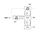
図1は、本発明の実施の形態に係る撮像装置の全体構成を示すブロック図である。 FIG. 1 is a block diagram showing an overall configuration of an imaging apparatus according to an embodiment of the present invention.
図1において、撮像装置100は、発光部101、レンズ102、アイリス103、アイリスモータ104、CMOSセンサ105、AD変換部106、欠陥検出部107、メモリ108、及び欠陥補正部109を備える。また、撮像装置100は、CPU110、絞り駆動回路111、及びCMOSセンサ駆動回路112を備える。
In FIG. 1, the
発光部101より出力される入射光は、レンズ102により結像され、アイリス103で入射光量を調節され、CMOSセンサ105へ入射される。CMOSセンサ105へ入射された入射光は、CMOSセンサ105で光電変換され、AD変換部106でAD変換され、デジタル化された映像データが欠陥検出部107及び欠陥補正部109へ入力される。
Incident light output from the
欠陥画素検出時、映像データにより欠陥検出部107において欠陥画素検出処理を行ない、その欠陥画素の情報はメモリ108に保持される。
When a defective pixel is detected, a defective pixel detection process is performed in the
欠陥画素補正時、映像データは欠陥補正部109へ入力され、欠陥画素検出時にメモリ108に保持したキズ情報に基づいて補正処理が施される。
At the time of defective pixel correction, the video data is input to the
CMOSセンサ駆動回路112は、CMOSセンサ105の蓄積動作、読み出し動作、リセット動作を制御する。
The CMOS
絞り駆動回路111は、アイリス102を駆動するアイリスモータ104を制御する。
The
CPU110は、シャッタ速度関連のパラメータからCMOSセンサ駆動回路112を制御し、絞り関連のパラメータにより絞り駆動回路111を制御する。
The
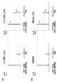
図2(a)及び(b)は、図1のCMOSセンサ105のフォトダイオード劣化要因の欠陥画素を説明する図であり、(a)はCMOSセンサ105の構成を示し、(b)は欠陥画素パターンを示す。
FIGS. 2A and 2B are diagrams for explaining a defective pixel that causes deterioration of the photodiode of the
図2(a)において、CMOSセンサ105は、フォトダイオード601、読み出し回路602、列アンプ603、垂直走査回路604、及び水平走査回路605を備える。
2A, the
フォトダイオード601は、撮像面に2次元に配列され、入射光を光電変換する。読み出し回路602は、複数のフォトダイオード601からの出力信号を読み出す。列アンプ603は、垂直方向の読み出し回路602からの出力信号を読み出す。
The
垂直走査回路604、及び水平走査回路605をドライブしてフォトダイオード601に蓄積された映像信号が順次出力される。
Video signals accumulated in the
図2(a)に示すように、フォトダイオード601a,601bが欠陥要因である場合、撮像面においての欠陥画素パターンは図2(b)に示すようになる。フォトダイオード601は画素ごとに独立しているので、孤立点欠陥となる可能性が高い。フォトダイオード601が欠陥要因である場合、暗電流特性がその原因であり、欠陥画素のセンサ出力(キズレベル)は蓄積時間や温度等の条件に依存する。そのため、フォトダイオード601が欠陥要因の欠陥画素には、リアルタイムの画素補間による補正が適している。また、条件によっては欠陥画素が目立たず補正を必要としない場合がある。
As shown in FIG. 2A, when the
図3(a)及び(b)は、図1のCMOSセンサ105の読み出し回路劣化要因の欠陥画素を説明する図であり、(a)はCMOSセンサ105の構成を示し、(b)は欠陥画素パターンを示す。
FIGS. 3A and 3B are diagrams for explaining a defective pixel that causes deterioration in the readout circuit of the
図3(a)に示すように、読み出し回路602aが欠陥要因である場合、欠陥画素パターンは図3(b)のようになる。読み出し回路602aは複数のフォトダイオード601が共有しているので、共有している画素分だけ欠陥画素が連続する。読み出し回路602が欠陥要因である場合、読み出し回路のトランジスタが故障して機能しないことが原因であるので、キズレベルは蓄積時間や温度に依存しない。そのため、読み出し回路602が欠陥要因の欠陥画素は、常時、周辺画素からの補間による補正が必要である。
As shown in FIG. 3A, when the
図4(a)及び(b)は、図1のCMOSセンサ105の列アンプ劣化要因の欠陥画素を説明する図であり、(a)はCMOSセンサ105の構成を示し、(b)は欠陥画素パターンを示す。
4A and 4B are diagrams for explaining a defective pixel that causes deterioration of the column amplifier of the
図4(a)に示すように、列アンプ603aが欠陥要因である場合、欠陥画素パターンは図4(b)のようになる。列アンプ603は垂直方向の全フォトダイオード601が共有しているので、完全な線キズとなる。列アンプ603が欠陥要因である場合、列アンプトランジスタの特性のばらつきが原因であり、キズレベルは蓄積時間や温度に依存しない。そのため、列アンプ603aが欠陥要因の欠陥画素には、キズレベルを事前に検出保持し、欠陥画素のキズレベル調整による補正が適している。
As shown in FIG. 4A, when the
図5は、図1のCMOSセンサ105における撮影条件と欠陥画素のセンサ出力(キズレベル)との関係を示す図である。
FIG. 5 is a diagram showing the relationship between the imaging conditions and the sensor output (scratch level) of the defective pixel in the
図5(a)は、蓄積時間とセンサ出力の関係を示す図である。 FIG. 5A is a diagram illustrating the relationship between the accumulation time and the sensor output.
図5(a)において、フォトダイオード601が欠陥要因である場合は、蓄積時間が2倍になると、センサ出力も比例して2倍になる。一方、読み出し回路602、又は列アンプ603が欠陥要因である場合は、センサ出力は蓄積時間に依存しない。
In FIG. 5A, when the
図5(b)は、温度とセンサ出力の関係を示す図である。 FIG. 5B is a diagram showing the relationship between temperature and sensor output.
図5(b)において、フォトダイオード601が欠陥要因である場合は、温度が高温(+8〜10℃)になると、センサ出力も2倍になる。一方、読み出し回路602、又は列アンプ603が欠陥要因である場合は、センサ出力は温度に依存しない。
In FIG. 5B, when the
図6は、図1の撮像装置100における欠陥検出時、欠陥補正時のデータの流れを説明する図である。
FIG. 6 is a diagram for explaining a data flow at the time of defect detection and defect correction in the
図6において、欠陥検出部107は、入力された映像データの欠陥画素の検出を行い、欠陥画素の位置情報(アドレス)、及びセンサ出力(レベル)をメモリ108に保存する。
In FIG. 6, the
CPU110は、絞り駆動回路111を制御して異なるシャッタ速度で複数回の欠陥画素検出処理を行うように制御し、それぞれのアドレス及びレベルをメモリ108に保存するようにする。また、CPU110は、各条件の同一アドレスの欠陥画素のレベルを比較すると共に、アドレスを参照することにより欠陥要因を判別し、判別結果に応じてキズフラグをメモリ108に保存する。
The
欠陥補正部109は、キズフラグをメモリ108より読み出し、各アドレスの欠陥要因を認知し、欠陥要因に応じた補正処理を行う。
The
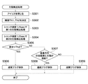
図7は、図1におけるCPU110で実行される欠陥検出処理のフローチャートである。
FIG. 7 is a flowchart of the defect detection process executed by the
図7において、CPU110は、絞り駆動回路111を制御してアイリス103を閉じ、CMOSセンサ105への入力を遮光状態とする(ステップS301)。次に、CPU110は、欠陥画素か否かを判別するための閾値Th1、及び欠陥要因がフォトダイオード601の劣化であるか否かを判別するための閾値Th2を決定する(ステップS302)。
In FIG. 7, the
CPU110は、CMOSセンサ駆動回路112のパラメータを制御し、シャッタ速度を1/4secとし、閾値Th1に基づいて第1の欠陥画素検出処理を行う(ステップS303)。この検出処理により、欠陥画素のアドレス及びレベルがメモリ108に保存される。
The
次に、CPU110は、CMOSセンサ駆動回路112のパラメータを制御し、シャッタ速度を1/2secとし、閾値Th1に基づいて第2の欠陥画素検出処理を行う(ステップS304)。この検出処理により、欠陥画素のアドレス及びレベルがメモリ108に保存される。
Next, the
次に、CPU110は、第1及び第2の欠陥画素検出処理における同一アドレスの欠陥画素のレベルを比較し、それらの差分が閾値Th2より大きいか否かを判別する(ステップS305)。
Next, the
ステップS305の判別の結果、差分が閾値Th2より大きいとき、すなわち、図5(a)に示すように、欠陥画素のレベルが2倍になり、欠陥画素のレベルがシャッタ速度に依存する場合は、フォトダイオード601の劣化が欠陥要因であると判別される。そのため、キズフラグとして通常フラグをメモリ108に保存し(ステップS306)、本処理を終了する。
As a result of the determination in step S305, when the difference is larger than the threshold value Th2, that is, as shown in FIG. 5A, when the level of the defective pixel is doubled and the level of the defective pixel depends on the shutter speed, It is determined that the deterioration of the
ステップS305の判別の結果、差分が閾値Th2より小さいとき、すなわち欠陥画素のレベルのシャッタ速度への依存度が少ない場合は、フォトダイオード601の劣化以外が欠陥要因であると判別され、ステップS307に進む。
As a result of the determination in step S305, when the difference is smaller than the threshold value Th2, that is, when the dependency of the defective pixel level on the shutter speed is small, it is determined that other than the deterioration of the
ステップS307では、撮像面における欠陥画素のアドレスのパターンマッチを行い、垂直方向の全画素に欠陥が連続するか否かを判別する。 In step S307, the pattern matching of the address of the defective pixel on the imaging surface is performed to determine whether or not the defect continues in all the pixels in the vertical direction.
ステップS307の判別の結果、垂直方向の全画素に欠陥が連続するときは、図4に示すように、列アンプ603の劣化が欠陥要因であると判別される。そのため、キズフラグとして連続フラグをメモリ108に保存し(ステップS308)、本処理を終了する。
As a result of the determination in step S307, when defects continue in all the pixels in the vertical direction, it is determined that the deterioration of the
ステップS307の判別の結果、垂直方向の全画素に欠陥が連続しないとき、すなわち、読み出し回路602を共有する画素分だけ欠陥が連続するときは、図3に示すように、読み出し回路602の劣化が欠陥要因であると判別される。そのため、キズフラグとして故障フラグをメモリ108に保存し(ステップS309)、本処理を終了する。
As a result of the determination in step S307, when the defect does not continue in all the pixels in the vertical direction, that is, when the defect continues for the pixels sharing the
図7の処理によれば、差分が閾値Th2より大きいとき、すなわち欠陥画素のレベルがシャッタ速度に依存する場合は(ステップS305でYES)、フォトダイオード601の劣化が欠陥要因であると判別される。これにより、欠陥画素が複数ある欠陥要因のうちのいずれによるものかを正確に判別し、欠陥要因に応じて補正方法を切り替えることにより画質を向上させることができる。
According to the process of FIG. 7, when the difference is larger than the threshold Th2, that is, when the level of the defective pixel depends on the shutter speed (YES in step S305), it is determined that the deterioration of the
図8は、図1におけるCPU110で実行される欠陥補正処理のフローチャートである。本処理は、図7の欠陥検出処理の後に実行される。
FIG. 8 is a flowchart of the defect correction process executed by the
図8において、CPU110は、欠陥画素のアドレス、レベル、及びキズフラグをメモリ108より読み込む(ステップS1001)。
In FIG. 8, the
次に、読み込んだキズフラグが通常フラグであるか否かを判別する(ステップS1002)。この判別の結果、読み込んだキズフラグが通常フラグであるとき、すなわち、フォトダイオード601の劣化が欠陥要因であるときは、ステップS1003に進む。
Next, it is determined whether or not the read scratch flag is a normal flag (step S1002). As a result of the determination, when the read scratch flag is a normal flag, that is, when deterioration of the
ステップS1003では、シャッタ速度が所定の閾値Thsより小さいか否かを判別する。この結果、シャッタ速度が所定の閾値Thsより小さいときは、温度が所定の閾値Thtより小さいか否かを判別する(ステップS1004)。この判別の結果、温度が所定の閾値Thtより小さいときは、キズは目立たず、補正処理を行うと補正による劣化が目立つと判断される。そのため、補正処理を行うことなく、本処理を終了する。 In step S1003, it is determined whether or not the shutter speed is smaller than a predetermined threshold value Ths. As a result, when the shutter speed is lower than the predetermined threshold Ths, it is determined whether or not the temperature is lower than the predetermined threshold Tht (step S1004). As a result of this determination, if the temperature is lower than the predetermined threshold value Tht, scratches are not noticeable, and it is determined that deterioration due to correction is noticeable when correction processing is performed. Therefore, this process is terminated without performing the correction process.
ステップS1003の判別の結果、シャッタ速度が所定の閾値Thsより大きいか、ステップS1004の判別の結果、温度が所定の閾値Thtより大きいときは、キズは目立つと判断され、ステップS1005に進む。 If the result of determination in step S1003 is that the shutter speed is greater than the predetermined threshold value Ths or the result of determination in step S1004 is that the temperature is greater than the predetermined threshold value Tht, it is determined that the scratch is conspicuous, and the process proceeds to step S1005.
ステップS1005では、周辺画素からの補間による補正処理を行い、本処理を終了する。 In step S1005, correction processing by interpolation from surrounding pixels is performed, and this processing ends.
ステップS1002の判別の結果、読み込んだキズフラグが通常フラグでないときは、読み込んだキズフラグが故障フラグであるか否かを判別する(ステップS1006)。この判別の結果、読み込んだキズフラグが故障フラグであるとき、すなわち、読み出し回路602の劣化が欠陥要因であるときは、周辺画素からの補間による補正処理を行い(ステップS1005)、本処理を終了する。
If the result of determination in step S1002 is that the read scratch flag is not a normal flag, it is determined whether or not the read scratch flag is a failure flag (step S1006). As a result of this determination, when the read flaw flag is a failure flag, that is, when deterioration of the
ステップS1006の判別の結果、読み込んだキズフラグが故障フラグでないとき(連続フラグであるとき)、すなわち、列アンプ603の劣化が欠陥要因であるときは、ステップS1007に進む。
As a result of the determination in step S1006, when the read scratch flag is not a failure flag (continuous flag), that is, when deterioration of the
ステップS1007では、メモリ108に保存している欠陥画素のレベルの減算による補正処理を行い、本処理を終了する。
In step S1007, a correction process is performed by subtracting the level of the defective pixel stored in the
図8の処理によれば、欠陥画素のアドレス、レベル、及びキズフラグをメモリ108より読み込む(ステップS1001)、読み込んだキズフラグに応じて補正処理を行う(ステップS1005、ステップS1007)。これにより、欠陥画素が複数ある欠陥要因のうちのいずれによるものかを正確に判別し、欠陥要因に応じて補正方法を切り替えることにより画質を向上させることができる。 According to the processing of FIG. 8, the address, level, and scratch flag of the defective pixel are read from the memory 108 (step S1001), and correction processing is performed according to the read scratch flag (step S1005, step S1007). Thereby, it is possible to accurately determine which of the plurality of defective pixels is due to a defect factor, and to improve the image quality by switching the correction method according to the defect factor.
図9は、図7の欠陥検出処理の変形例のフローチャートである。 FIG. 9 is a flowchart of a modification of the defect detection process of FIG.
図9において、CPU110は、絞り駆動回路111を制御してアイリス103を閉じ、CMOSセンサ105への入力を遮光状態とする(ステップS501)。次に、CPU110は、欠陥画素か否かを判別するための閾値Th1、及び欠陥要因がフォトダイオード601の劣化であるか否かを判別するための閾値Th2を決定する(ステップS502)。
In FIG. 9, the
CPU110は、CMOSセンサ駆動回路112のパラメータを制御し、シャッタ速度を1/2secとし、温度を20℃に設定して、閾値Th1に基づいて第1の欠陥画素検出処理を行う(ステップS503)。この検出処理により、欠陥画素のアドレス及びレベルがメモリ108に保存される。
The
次に、CPU110は、CMOSセンサ駆動回路112のパラメータを制御し、温度を28℃に設定して、閾値Th1に基づいて第2の欠陥画素検出処理を行う(ステップS504)。この検出処理により、欠陥画素のアドレス及びレベルがメモリ108に保存される。
Next, the
次に、CPU110は、第1及び第2の欠陥画素検出処理における同一アドレスの欠陥画素のレベルを比較し、それらの差分が閾値Th2より大きいか否かを判別する(ステップS505)。
Next, the
ステップS505の判別の結果、差分が閾値Th2より大きいとき、すなわち、図5(b)に示すように、欠陥画素のレベルが2倍になり、欠陥画素のレベルが温度に依存する場合は、フォトダイオード601の劣化が欠陥要因であると判別される。そのため、キズフラグとして通常フラグをメモリ108に保存し(ステップS506)、本処理を終了する。
As a result of the determination in step S505, when the difference is larger than the threshold Th2, that is, as shown in FIG. 5B, the level of the defective pixel is doubled and the level of the defective pixel depends on the temperature. It is determined that the deterioration of the
ステップS505の判別の結果、差分が閾値Th2より小さいとき、すなわち欠陥画素のレベルの温度への依存度が少ない場合は、フォトダイオード601の劣化以外が欠陥要因であると判別され、ステップS507に進む。
As a result of the determination in step S505, when the difference is smaller than the threshold Th2, that is, when the dependency of the level of the defective pixel on the temperature is small, it is determined that other than the deterioration of the
ステップS507では、撮像面における欠陥画素のアドレスのパターンマッチを行い、垂直方向の全画素に欠陥が連続するか否かを判別する。 In step S507, the pattern matching of the defective pixel address on the imaging surface is performed to determine whether or not the defect continues in all the pixels in the vertical direction.
ステップS507の判別の結果、垂直方向の全画素に欠陥が連続するときは、図4に示すように、列アンプ603の劣化が欠陥要因であると判別される。そのため、キズフラグとして連続フラグをメモリ108に保存し(ステップS508)、本処理を終了する。
As a result of the determination in step S507, when defects continue in all the pixels in the vertical direction, it is determined that the deterioration of the
ステップS507の判別の結果、垂直方向の全画素に欠陥が連続しないとき、すなわち、読み出し回路602を共有する画素分だけ欠陥が連続するときは、図3に示すように、読み出し回路602の劣化が欠陥要因であると判別される。そのため、キズフラグとして故障フラグをメモリ108に保存し(ステップS509)、本処理を終了する。
As a result of the determination in step S507, when the defect does not continue in all the pixels in the vertical direction, that is, when the defect continues for the pixels sharing the
図9の処理によれば、差分が閾値Th2より大きいとき、すなわち欠陥画素のレベルが温度に依存する場合は(ステップS505でYES)、フォトダイオード601の劣化が欠陥要因であると判別される。これにより、欠陥画素が複数ある欠陥要因のうちのいずれによるものかを正確に判別し、欠陥要因に応じて補正方法を切り替えることにより画質を向上させることができる。
According to the process of FIG. 9, when the difference is larger than the threshold Th2, that is, when the level of the defective pixel depends on the temperature (YES in step S505), it is determined that the deterioration of the
図10は、図7の欠陥検出処理の他の変形例のフローチャートである。 FIG. 10 is a flowchart of another modification of the defect detection process of FIG.
図10において、CPU110は、絞り駆動回路111を制御してアイリス103を閉じ、CMOSセンサ105への入力を遮光状態とする(ステップS401)。次に、CPU110は、欠陥画素か否かを判別するための閾値Th1、及び欠陥要因がフォトダイオード601の劣化であるか否かを判別するための閾値Th2を決定する(ステップS402)。
In FIG. 10, the
CPU110は、CMOSセンサ駆動回路112のパラメータを制御し、シャッタ速度を1/2secとし、欠陥画素検出処理を行う(ステップS403)。この検出処理により、欠陥画素のアドレス及びレベルがメモリ108に保存される。
The
次に、撮像面における欠陥画素のアドレスのパターンマッチを行う(ステップS404)。この判別の結果、欠陥画素が孤立しているときは、図2に示すように、フォトダイオード601の劣化が欠陥要因であると判別される。そのため、キズフラグとして通常フラグをメモリ108に保存し(ステップS405)、本処理を終了する。
Next, pattern matching is performed on the address of the defective pixel on the imaging surface (step S404). If the defective pixel is isolated as a result of this determination, it is determined that the deterioration of the
ステップS404の判別の結果、垂直方向の全画素に欠陥が連続するときは、パターン内の欠陥画素のレベルのばらつきが閾値Th2より大きいか否かを判別する(ステップS406)。 If the result of determination in step S404 is that a defect continues in all the pixels in the vertical direction, it is determined whether or not the level variation of the defective pixel in the pattern is greater than the threshold Th2 (step S406).
ステップS406の判別の結果、パターン内の欠陥画素のレベルのばらつきが閾値Th2より小さいときは、図4に示すように、列アンプ603の劣化が欠陥要因であると判別される。そのため、キズフラグとして連続フラグをメモリ108に保存し(ステップS407)、本処理を終了する。
If the result of determination in step S406 is that the variation in level of defective pixels in the pattern is smaller than the threshold Th2, it is determined that the deterioration of the
ステップS406の判別の結果、パターン内の欠陥画素のレベルのばらつきが閾値Th2より大きいときは、フォトダイオード601の劣化が欠陥要因の欠陥画素が偶然連続したものと判別し、ステップS405以降の処理を実行する。
As a result of the determination in step S406, when the variation in the level of the defective pixel in the pattern is larger than the threshold Th2, it is determined that the defective pixel due to the defect of the
ステップS404の判別の結果、読み出し回路602を共有する画素分だけ欠陥が連続するときは、パターン内の欠陥画素のレベルのばらつきが閾値Th2より大きいか否かを判別する(ステップS408)。
As a result of the determination in step S404, if defects continue for the number of pixels sharing the
ステップS408の判別の結果、パターン内の欠陥画素のレベルのばらつきが閾値Th2より小さいときは、図3に示すように、読み出し回路602の劣化が欠陥要因であると判別される。そのため、キズフラグとして故障フラグをメモリ108に保存し(ステップS409)、本処理を終了する。
As a result of the determination in step S408, when the variation in the level of the defective pixel in the pattern is smaller than the threshold Th2, it is determined that the deterioration of the
ステップS408の判別の結果、パターン内の欠陥画素のレベルのばらつきが閾値Th2より大きいときは、フォトダイオード601の劣化が欠陥要因の欠陥画素が偶然連続したものと判別し、ステップS405以降の処理を実行する。
As a result of the determination in step S408, when the variation in the level of the defective pixel in the pattern is larger than the threshold value Th2, it is determined that the defective pixel due to the defect of the
図10の処理によれば、欠陥画素が孤立しているときは、フォトダイオード601の劣化が欠陥要因であると判別される(ステップS404)。これにより、欠陥画素が複数ある欠陥要因のうちのいずれによるものかを正確に判別し、欠陥要因に応じて補正方法を切り替えることにより画質を向上させることができる。
According to the process of FIG. 10, when the defective pixel is isolated, it is determined that the deterioration of the
上記の実施の形態で説明した処理、機能等は、いずれもコンピュータ読み取り可能なプログラム等で実現することもできる。 Any of the processes, functions, and the like described in the above embodiments can be realized by a computer-readable program or the like.
この場合、上記の実施の形態で説明した処理、機能等は、システム又は装置に含まれるコンピュータ(CPU、MPU等でもよい)が上記のプログラム等を実行することによって実現されることになる。言い換えれば、上記のプログラム等が、システム又は装置に含まれるコンピュータに、上記の実施の形態で説明した処理、機能等を実行させることになる。また、この場合、上記のプログラム等は、コンピュータ読み取り可能な記憶媒体又はネットワークを介してシステム又は装置に含まれるコンピュータに提供されることになる。 In this case, the processes, functions, and the like described in the above embodiments are realized when a computer (CPU, MPU, or the like) included in the system or apparatus executes the above programs. In other words, the above-described program or the like causes the computer included in the system or apparatus to execute the processes and functions described in the above-described embodiment. In this case, the above-described program or the like is provided to a computer included in the system or apparatus via a computer-readable storage medium or a network.
システム又は装置に含まれるコンピュータに上記のプログラム等を提供する記憶媒体には、磁気ディスク、光ディスク、光磁気ディスク、ハードディスク、磁気テープ、不揮発性メモリ等を用いることができる。 A magnetic disk, an optical disk, a magneto-optical disk, a hard disk, a magnetic tape, a nonvolatile memory, or the like can be used as a storage medium that provides the above-described program or the like to a computer included in the system or apparatus.
また、上記のプログラム等は、その一部をコンピュータ上で稼動しているOS(オペレーティングシステム)等を用いて構成してもよい。 Moreover, you may comprise a part of said program etc. using OS (operating system) etc. which are operate | moving on the computer.
さらに、上記のプログラム等は、その一部をコンピュータに挿入された機能拡張ボードやコンピュータに接続された機能拡張ユニットで実行するように構成してもよい。 Furthermore, a part of the above-described program may be executed by a function expansion board inserted into the computer or a function expansion unit connected to the computer.
100 撮像装置
107 欠陥検出部
108 メモリ
109 欠陥補正部
110 CPU
DESCRIPTION OF
Claims (11)
前記取得された複数の映像データからそれぞれ欠陥画素を検出して前記欠陥画素の出力のレベルを取得する検出手段と、
前記複数の映像データからそれぞれ検出された前記欠陥画素の出力のレベルの差分に基づいて、前記検出された欠陥画素の欠陥要因を判別する判別手段とを備えることを特徴とする撮像装置。 An acquisition unit configured to acquire a plurality of image data obtained under different conditions from the sensor,
Detecting means for detecting a defective pixel from each of the plurality of acquired video data and acquiring an output level of the defective pixel;
An imaging apparatus comprising: a discriminating unit that discriminates a defect factor of the detected defective pixel based on a difference in output level of the defective pixel detected from each of the plurality of video data.
前記判別手段は、前記複数の映像データからそれぞれ検出された前記欠陥画素の出力のレベルの差分、および、前記取得された前記欠陥画素のアドレスが連続するか否かに基づいて、前記検出された欠陥画素の欠陥要因を判別することを特徴とする請求項1に記載の撮像装置。 The detecting means acquires the addresses of the defective pixels of each detected,
The determination means is detected based on a difference in output level of the defective pixel detected from each of the plurality of video data, and whether or not the acquired address of the defective pixel is continuous. the imaging apparatus according to claim 1, characterized that you determine the defect factor of the defective pixel.
前記判別手段は、前記取得された前記欠陥画素のアドレスが、少なくとも読み出し回路を共有する画素において連続している場合に、前記検出された欠陥画素の欠陥要因が、前記読み出し回路によるものであると判別することを特徴とする請求項6記載の撮像装置。 Said sensor, CMOS sensor, comprising: a photodiode for photoelectrically converting an image focused by the lenses, and a read circuit for reading an output signal from the photodiode, and a column amplifier to read the output signal from the readout circuit And
In the determination unit, when the acquired address of the defective pixel is continuous in at least pixels sharing the readout circuit, the defect factor of the detected defective pixel is due to the readout circuit. The imaging device according to claim 6 , wherein the imaging device is discriminated.
前記取得された複数の映像データからそれぞれ欠陥画素を検出して前記欠陥画素の出力のレベルを取得する検出ステップと、
前記複数の映像データからそれぞれ検出された前記欠陥画素の出力のレベルの差分に基づいて、前記検出された欠陥画素の欠陥要因を判別する判別ステップとを備えることを特徴とする撮像装置の欠陥画素の判別方法。 An acquisition step of acquiring a plurality of image data obtained under different conditions from the sensor,
A detecting step of detecting a defective pixel from each of the plurality of acquired video data and acquiring an output level of the defective pixel;
A defective pixel of the imaging apparatus, comprising: a determination step of determining a defect factor of the detected defective pixel based on a difference in output level of the defective pixel detected from each of the plurality of video data. How to determine.
Priority Applications (1)
| Application Number | Priority Date | Filing Date | Title |
|---|---|---|---|
| JP2006334741A JP5028077B2 (en) | 2006-12-12 | 2006-12-12 | Imaging device, method for determining defective pixel thereof, and program |
Applications Claiming Priority (1)
| Application Number | Priority Date | Filing Date | Title |
|---|---|---|---|
| JP2006334741A JP5028077B2 (en) | 2006-12-12 | 2006-12-12 | Imaging device, method for determining defective pixel thereof, and program |
Publications (3)
| Publication Number | Publication Date |
|---|---|
| JP2008148129A JP2008148129A (en) | 2008-06-26 |
| JP2008148129A5 JP2008148129A5 (en) | 2010-02-04 |
| JP5028077B2 true JP5028077B2 (en) | 2012-09-19 |
Family
ID=39607788
Family Applications (1)
| Application Number | Title | Priority Date | Filing Date |
|---|---|---|---|
| JP2006334741A Expired - Fee Related JP5028077B2 (en) | 2006-12-12 | 2006-12-12 | Imaging device, method for determining defective pixel thereof, and program |
Country Status (1)
| Country | Link |
|---|---|
| JP (1) | JP5028077B2 (en) |
Families Citing this family (2)
| Publication number | Priority date | Publication date | Assignee | Title |
|---|---|---|---|---|
| JP6848421B2 (en) * | 2016-12-21 | 2021-03-24 | 株式会社リコー | Photoelectric conversion device, photoelectric conversion method and image forming device |
| JP6992521B2 (en) * | 2017-01-25 | 2022-01-13 | 株式会社リコー | Photoelectric conversion device, defect pixel determination method and image forming device |
Family Cites Families (5)
| Publication number | Priority date | Publication date | Assignee | Title |
|---|---|---|---|---|
| JPH09289614A (en) * | 1996-04-24 | 1997-11-04 | Matsushita Electric Ind Co Ltd | Solid-state image pickup device |
| JP3601908B2 (en) * | 1996-07-30 | 2004-12-15 | 東芝医用システムエンジニアリング株式会社 | Image processing device defective pixel correction processing device, X-ray diagnostic device |
| JP3876400B2 (en) * | 1999-06-23 | 2007-01-31 | 富士通株式会社 | Infrared imaging device and element defect compensation method |
| JP2002354340A (en) * | 2001-05-24 | 2002-12-06 | Olympus Optical Co Ltd | Imaging device |
| JP2004327722A (en) * | 2003-04-24 | 2004-11-18 | Matsushita Electric Ind Co Ltd | Inspection method of solid-state imaging device |
-
2006
- 2006-12-12 JP JP2006334741A patent/JP5028077B2/en not_active Expired - Fee Related
Also Published As
| Publication number | Publication date |
|---|---|
| JP2008148129A (en) | 2008-06-26 |
Similar Documents
| Publication | Publication Date | Title |
|---|---|---|
| JP5300356B2 (en) | IMAGING DEVICE AND IMAGING DEVICE CONTROL METHOD | |
| JP5379601B2 (en) | Defective pixel data correction device, imaging device, and defective pixel data correction method | |
| JP5311945B2 (en) | Imaging apparatus and defective pixel detection method | |
| JP5013812B2 (en) | Imaging apparatus and correction method | |
| JP2005123946A (en) | Defective pixel detection method, detector and imaging apparatus | |
| JP2010245891A (en) | Imaging device and imaging method | |
| JP2007174266A (en) | Imaging apparatus | |
| JP5028077B2 (en) | Imaging device, method for determining defective pixel thereof, and program | |
| JP2005175930A (en) | Image pickup device, its signal processing method, and image pickup system | |
| JP2008312169A (en) | Image processing apparatus and method, and imaging apparatus | |
| JP4471352B2 (en) | Defective pixel correction apparatus and method, imaging apparatus, program, and storage medium | |
| JP2006157242A (en) | Clamping unit and method for image signal | |
| JP4785564B2 (en) | Defect correction apparatus and defect correction method | |
| JP4394470B2 (en) | Imaging device | |
| JP2006345279A (en) | Method of detecting pixel defect for solid state imaging device | |
| JP5968145B2 (en) | Image processing apparatus and control method thereof | |
| JP6218408B2 (en) | Image processing apparatus, image processing method, and program | |
| JP2005341261A (en) | Imaging unit | |
| JP2012124778A (en) | Imaging apparatus, imaging processing method, and computer program | |
| JP2004023231A (en) | Imaging device and portable telephone system provided with the imaging device | |
| JP4481764B2 (en) | Method for correcting signal output from image sensor and image processing apparatus using the same | |
| JP6765953B2 (en) | Imaging device and its control method | |
| JP2008017246A (en) | Inspecting method and device for solid imaging device | |
| JP6320086B2 (en) | Imaging apparatus and control method thereof | |
| JP2005102314A (en) | Pixel defect detecting method for solid-state image sensor, and imaging device using the method |
Legal Events
| Date | Code | Title | Description |
|---|---|---|---|
| A521 | Request for written amendment filed |
Free format text: JAPANESE INTERMEDIATE CODE: A523 Effective date: 20091210 |
|
| A621 | Written request for application examination |
Free format text: JAPANESE INTERMEDIATE CODE: A621 Effective date: 20091210 |
|
| A977 | Report on retrieval |
Free format text: JAPANESE INTERMEDIATE CODE: A971007 Effective date: 20111213 |
|
| A131 | Notification of reasons for refusal |
Free format text: JAPANESE INTERMEDIATE CODE: A131 Effective date: 20111222 |
|
| A521 | Request for written amendment filed |
Free format text: JAPANESE INTERMEDIATE CODE: A523 Effective date: 20120216 |
|
| TRDD | Decision of grant or rejection written | ||
| A01 | Written decision to grant a patent or to grant a registration (utility model) |
Free format text: JAPANESE INTERMEDIATE CODE: A01 Effective date: 20120619 |
|
| A01 | Written decision to grant a patent or to grant a registration (utility model) |
Free format text: JAPANESE INTERMEDIATE CODE: A01 |
|
| A61 | First payment of annual fees (during grant procedure) |
Free format text: JAPANESE INTERMEDIATE CODE: A61 Effective date: 20120625 |
|
| FPAY | Renewal fee payment (event date is renewal date of database) |
Free format text: PAYMENT UNTIL: 20150629 Year of fee payment: 3 |
|
| R151 | Written notification of patent or utility model registration |
Ref document number: 5028077 Country of ref document: JP Free format text: JAPANESE INTERMEDIATE CODE: R151 |
|
| LAPS | Cancellation because of no payment of annual fees |