JP5379601B2 - Defective pixel data correction device, imaging device, and defective pixel data correction method - Google Patents
Defective pixel data correction device, imaging device, and defective pixel data correction method Download PDFInfo
- Publication number
- JP5379601B2 JP5379601B2 JP2009184830A JP2009184830A JP5379601B2 JP 5379601 B2 JP5379601 B2 JP 5379601B2 JP 2009184830 A JP2009184830 A JP 2009184830A JP 2009184830 A JP2009184830 A JP 2009184830A JP 5379601 B2 JP5379601 B2 JP 5379601B2
- Authority
- JP
- Japan
- Prior art keywords
- defective pixel
- defective
- correction
- imaging
- pixels
- Prior art date
- Legal status (The legal status is an assumption and is not a legal conclusion. Google has not performed a legal analysis and makes no representation as to the accuracy of the status listed.)
- Expired - Fee Related
Links
Images


Classifications
-
- H—ELECTRICITY
- H04—ELECTRIC COMMUNICATION TECHNIQUE
- H04N—PICTORIAL COMMUNICATION, e.g. TELEVISION
- H04N25/00—Circuitry of solid-state image sensors [SSIS]; Control thereof
- H04N25/60—Noise processing, e.g. detecting, correcting, reducing or removing noise
- H04N25/68—Noise processing, e.g. detecting, correcting, reducing or removing noise applied to defects
- H04N25/683—Noise processing, e.g. detecting, correcting, reducing or removing noise applied to defects by defect estimation performed on the scene signal, e.g. real time or on the fly detection
Description
本発明は、欠陥画素データ補正装置、撮像装置及び欠陥画素データ補正方法に関し、特には撮像素子の欠陥画素の補正技術に関する。 The present invention relates to a defective pixel data correction apparatus, an imaging apparatus, and a defective pixel data correction method, and more particularly to a technique for correcting defective pixels of an imaging element.
デジタルカメラやデジタルビデオカメラなどには、CMOSイメージセンサやCCDイメージセンサを代表とする撮像素子が用いられている。撮像素子には数十万〜数千万の画素が配列されるが、素子を形成する物質の結晶欠陥やダストなどの影響により、画素として出力すべき信号(以下、正規の出力信号と呼ぶ)を発生しない画素が含まれる。このような画素は欠陥画素と呼ばれており、本明細書では、欠陥画素が出力する正規でない信号を異常出力信号と呼ぶ。なお、異常出力信号の出力とは、信号が全く出力されない状態を含みうる。 For digital cameras, digital video cameras, and the like, image sensors represented by CMOS image sensors and CCD image sensors are used. Hundreds of thousands to tens of millions of pixels are arranged in the image sensor, but a signal to be output as a pixel due to the influence of crystal defects or dust of the substance forming the element (hereinafter referred to as a normal output signal) Pixels that do not generate are included. Such a pixel is called a defective pixel, and in this specification, an irregular signal output from a defective pixel is called an abnormal output signal. The output of the abnormal output signal can include a state where no signal is output.
欠陥画素は、定常的に異常出力信号を出力する定常欠陥画素と、正規の出力信号と異常出力信号とを非定常的に出力する点滅欠陥画素に大別される。
CMOSイメージセンサでは、定常欠陥画素と点滅欠陥画素では、異常信号の出力特性が異なることが知られている。定常欠陥画素では、ダスト、開口むら等の感度依存性欠陥画素を除いた場合、受光部の結晶欠陥による白点欠陥が多数を占める。よって、本明細書では、白点欠陥画素を定常欠陥画素と定義する。白点欠陥画素は暗信号の増加を伴うため、異常信号出力レべルは、欠陥画素の温度および欠陥画素の電荷蓄積時間に依存した特性を有する。
一方、点滅欠陥画素は結晶欠陥が発生する箇所が定常欠陥画素と異なるため、異常出力信号レべルの特性は欠陥画素の温度および電荷蓄積時間にほとんど依存しない。
The defective pixels are roughly classified into a steady defective pixel that outputs an abnormal output signal constantly and a blinking defective pixel that outputs a normal output signal and an abnormal output signal non-steadyly.
In a CMOS image sensor, it is known that output characteristics of abnormal signals are different between a steady defective pixel and a blinking defective pixel. In stationary defect pixels, when sensitivity-dependent defect pixels such as dust and aperture unevenness are excluded, white spot defects due to crystal defects in the light receiving portion occupy a large number. Therefore, in this specification, a white point defective pixel is defined as a steady defective pixel. Since white point defective pixels are accompanied by an increase in dark signal, the abnormal signal output level has characteristics depending on the temperature of the defective pixels and the charge accumulation time of the defective pixels.
On the other hand, the blinking defective pixel is different from the stationary defective pixel in the location where the crystal defect occurs, and therefore the characteristic of the abnormal output signal level hardly depends on the temperature of the defective pixel and the charge accumulation time.
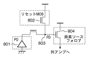
図6に示す、CMOSイメージセンサの画素の一般的な回路構成において、801は受光部であるフォトダイオード(PD)、802は蓄積された電荷をリセットするリセットMOSである。また、803は電荷検出を行うフローティングディフュージョン(FD)、804は画素ソースフォロアである。
In the general circuit configuration of the pixel of the CMOS image sensor shown in FIG. 6,
そして、定常欠陥画素の多くは、PD801の結晶欠陥に因って発生するのに対し、点滅欠陥画素は、画素ソースフォロア804を構成するMOSトランジスタの界面順位で、電子が捕獲、放出を繰り返すことで発生すると考えられている。点滅欠陥画素の異常出力信号レベルは、異常の原因が画素ソースフォロア804であるため、温度や電荷蓄積時間にほとんど依存しない。
Most of the stationary defective pixels are generated due to crystal defects of the
従来、欠陥画素の種類に応じて補正方法を変更し、点滅欠陥画素と定常欠陥画素とを適切に補正しようとする技術が提案されている(特許文献1参照)。 Conventionally, a technique has been proposed in which the correction method is changed in accordance with the type of defective pixel to appropriately correct the blinking defective pixel and the steady defective pixel (see Patent Document 1).
しかし、特許文献1では、点滅欠陥画素と常時欠陥画素とで異常信号出力レベルの画素温度や電荷蓄積時間に対する依存性が異なることについては特に考慮していない。そのため、欠陥画素検出時と被写体撮像時とで画素温度や電荷蓄積時間が異なる場合、上述した依存性の相違から、特に点滅欠陥画素に対する補正が適切に行われない可能性がある。例えば、温度及び電荷蓄積時間に対する依存性の大きな定常欠陥画素を基準として補正すべき欠陥画素を選択した場合、補正すべき点滅欠陥画素が選択されなかったり、補正すべきでない点滅欠陥画素が選択されたりする。前者の場合、補正残りが発生するため、画像のノイズが十分補正されず、後者の場合は不要な補正が行われるため画像の解像度が劣化するという問題がある。
However,
本発明はこのような従来技術の課題に鑑みなされたものである。本発明は、異常信号出力レベルの撮像条件に対する依存性が欠陥画素の種類によって異なることを考慮して適切な欠陥画素補正を行う欠陥画素データ補正装置及びそれを備える撮像装置、並びに欠陥画素データ補正方法を提供する。 The present invention has been made in view of the problems of the prior art. The present invention relates to a defective pixel data correction device that performs appropriate defective pixel correction in consideration of the dependency of the abnormal signal output level on the imaging condition depending on the type of defective pixel, an imaging device including the same, and defective pixel data correction Provide a method.
本発明のある見地によれば、複数の画素からなる撮像素子を用いて撮像される画像データに含まれる、撮像素子の欠陥画素から出力される欠陥画素データを補正する欠陥画素データ補正装置であって、複数の画素に含まれる各欠陥画素についての欠陥画素の種類及び欠陥出力レベルを含む欠陥画素情報を記憶した欠陥画素情報記憶手段と、欠陥画素の種類の各々に対応し、撮像条件と補正対象となる欠陥出力レベルとの関係を表す複数の補正テーブルを記憶した補正テーブル記憶手段と、欠陥画素情報と、複数の補正テーブルのうち欠陥画素の種類に対応した補正テーブルとに基づいて、欠陥画素データの補正要否を判定する判定手段と、判定手段により補正要と判定された欠陥画素データを補正する補正手段と、を有することを特徴とする欠陥画素データ補正装置が提供される。 According to an aspect of the present invention, there is provided a defective pixel data correction device that corrects defective pixel data output from a defective pixel of an image sensor, which is included in image data captured using an image sensor composed of a plurality of pixels. A defective pixel information storage means for storing defective pixel information including a defective pixel type and a defective output level for each defective pixel included in a plurality of pixels, and an imaging condition and correction corresponding to each of the defective pixel types. Based on the correction table storage means storing a plurality of correction tables representing the relationship with the target defect output level, defect pixel information, and a correction table corresponding to the type of defective pixel among the plurality of correction tables. and having a determining means for correcting necessity of pixel data, and a correction means for correcting the determined defective pixel data correction necessity by determining means Recessed pixel data correction device is provided.
このような構成により、本発明によれば、異常信号出力レベルの撮像条件に対する依存性が欠陥画素の種類によって異なることを考慮して適切な欠陥画素補正を行うことが可能になる。 With such a configuration, according to the present invention, it is possible to perform appropriate defective pixel correction in consideration of the dependency of the abnormal signal output level on the imaging condition depending on the type of defective pixel.
以下、添付図面を参照して、本発明の例示的な実施形態を説明する。
図1は、本発明の一実施形態に係る欠陥画素データ補正装置、を備える撮像装置の一例としてのデジタルスチルカメラ120の構成例を示すブロック図である。
Hereinafter, exemplary embodiments of the present invention will be described with reference to the accompanying drawings.
FIG. 1 is a block diagram illustrating a configuration example of a
撮像素子102は光電変換素子であり、被写体光学像を画素単位のアナログ映像信号に変換して出力する。撮像素子102は、例えばCMOSイメージセンサである。レンズ100は、被写体光学像を撮像素子102上に結像する。メカニカルシャッター(メカシャッター)101は、レンズ100と撮像素子102との間の光路を開閉させる。タイミングジェネレータ(TG)103は、撮像素子102の駆動信号を生成する。
The
A/D変換回路104は、撮像素子102から出力されるアナログ画像信号をデジタル画像信号に変換する。記憶部105の画像用メモリ106は、デジタル画像信号をRAW画像データとして一時記憶する。記憶部105は、例えば半導体記憶装置から構成される。また、画像用メモリ106は、例えばDRAMである。
The A /
記憶部105は、画像用メモリ106、欠陥画素情報メモリ107(欠陥画素情報記憶手段)、欠陥画素補正テーブル108(補正テーブル記憶手段)、欠陥画素検出条件テーブル109を有する。記憶部105の詳細な動作については後述する。
The
欠陥画素判定回路110(判定手段)は、欠陥画素をその種類とともに判別し、さらに異常出力信号レベル(欠陥出力レベル)を判定する。本実施形態では、欠陥画素判定回路110は、検出された欠陥画素が点滅欠陥画素と定常欠陥画素のいずれであるのかを判別する。なお、他の欠陥画素を判別可能に構成してもよい。
欠陥画素補正回路111(補正手段)は、欠陥画素判定回路110で欠陥画素であると判定された画素について、その種類に応じた補正を行う。
The defective pixel determination circuit 110 (determination unit) determines defective pixels together with their types, and further determines an abnormal output signal level (defective output level). In the present embodiment, the defective
The defective pixel correction circuit 111 (correction unit) performs correction according to the type of the pixel determined to be a defective pixel by the defective
画像処理回路112は、画像用メモリ106に一時記憶されたRAW画像データに予め定められた画像処理を施し、最終的な出力画像フォーマット、例えばDCFに準拠したJPEG形式に変換する。ここで、DCFとは、デジタルカメラ用画像フォーマット(Design rule for Camera File system)の略である。そして、画像処理回路112は、最終的な出力画像フォーマットに変換した撮像画像を記憶媒体113に記憶する。記憶媒体113は、例えば半導体メモリカードである。
温度検出部115は、撮像素子102の温度または撮像素子102近傍の温度(周辺温度)を検出する。温度検出部115は、例えばサーミスタである。
The
The
制御部114は、例えばCPU、ROM及びRAMを含み、ROMに記憶されたプログラムをRAMに展開してCPUで実行する。そして、後述する欠陥画素の検出処理や補正処理を始めとしたデジタルスチルカメラ全体の動作を司る。
The
操作部116は、電源ON/OFFボタン、シャッターボタン、メニューボタン、方向キー、決定ボタンなど、各種ボタンやキーなどの入力デバイス群である。操作者により操作部116が操作されると、操作されたことが制御部114によって検出される。そして、制御部114が操作内容を判別してデジタルスチルカメラ120に各種指示を出力する。
The operation unit 116 is an input device group such as various buttons and keys such as a power ON / OFF button, a shutter button, a menu button, a direction key, and a determination button. When the operation unit 116 is operated by the operator, the operation is detected by the
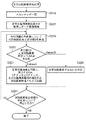
●(欠陥画素検出処理)
次に、図2A及び図2Bのフローチャートを用いて、本実施形態におけるデジタルスチルカメラが行う欠陥画素検出方法の一例を説明する。ここで、欠陥画素検出条件テーブル109、欠陥画素判定回路110、及び制御部114が欠陥画素検出手段を構成する。
● (Defect pixel detection processing)
Next, an example of a defective pixel detection method performed by the digital still camera according to the present embodiment will be described using the flowcharts of FIGS. 2A and 2B. Here, the defective pixel detection condition table 109, the defective
本実施形態における欠陥画素検出処理は、点滅欠陥画素の検出処理と定常欠陥画素の検出処理からなる。上述の通り、点滅欠陥画素と定常欠陥画素は、異常出力信号レベルの出力特性が、温度及び電荷蓄積時間に対して異なる依存性を有する。そこで、本実施形態では、点滅欠陥画素と定常欠陥画素とで欠陥画素検出条件を異ならせている。 The defective pixel detection process in the present embodiment includes a blinking defective pixel detection process and a steady defective pixel detection process. As described above, the blinking defective pixel and the steady defective pixel have different dependency of the output characteristics of the abnormal output signal level on the temperature and the charge accumulation time. Therefore, in the present embodiment, the defective pixel detection condition is made different between the blinking defective pixel and the steady defective pixel.
ここで、本実施形態では、図6における画素ソースフォロア804のMOSトランジスタの界面順位で電子の捕獲と放出を繰り返す白点欠陥画素、または黒点欠陥画素を点滅欠陥画素と定義する。また、図6におけるPD801の結晶欠陥による白点欠陥画素を定常欠陥画素と定義する。なお、欠陥画素の種類は、定常欠陥画素と点滅欠陥画素の2種類に限らず、3種類以上に分類しても構わない。
Here, in this embodiment, a white spot defective pixel or a black spot defective pixel that repeats electron capture and emission in accordance with the interface order of the MOS transistors of the
図2Aは、点滅欠陥画素検出処理の詳細を説明するフローチャートである。
撮像者が操作部116に含まれる電源ON/OFFボタンを操作して、デジタルスチルカメラ120の電源オンを指示すると、制御部114はカメラの起動処理を開始する。そして、制御部114は、起動処理の一部として、図2Aに示す点滅欠陥画素検出処理を実行する。
FIG. 2A is a flowchart illustrating details of the blinking defective pixel detection process.
When the photographer operates the power ON / OFF button included in the operation unit 116 to instruct the power on of the digital
上述の通り、点滅欠陥画素の異常出力信号レベルは温度依存性がほとんどない。そのため、本実施形態では、定常欠陥画素の影響を受けにくい、デジタルスチルカメラ(特に、撮像素子102の近傍)の温度が低い状態にあると想定される、電源オン動作時に点滅欠陥画素を検出する。 As described above, the abnormal output signal level of the blinking defective pixel has almost no temperature dependence. For this reason, in the present embodiment, it is assumed that the temperature of the digital still camera (particularly, in the vicinity of the image sensor 102) is low, which is not easily affected by the stationary defective pixel, and the blinking defective pixel is detected during the power-on operation. .
S203において、欠陥画素検出用ダーク画像撮像のためにメカシャッター101を閉じる。次に、S205において、点滅欠陥画素検出条件を欠陥画素検出条件テーブル109から取得し、取得した欠陥画素検出条件でダークRAW画像を撮像する。
In S203, the
図4は、欠陥画素検出条件テーブル109に含まれる、点滅欠陥画素検出のための撮像条件と、定常欠陥画素検出のための撮像条件の一例である。ここでは、図4の点滅欠陥画素検出のための撮像条件に基づいて、ダークRAW画像を撮像する。 FIG. 4 is an example of imaging conditions for detecting blinking defective pixels and imaging conditions for detecting steady defective pixels, which are included in the defective pixel detection condition table 109. Here, a dark RAW image is captured based on the imaging condition for detecting the blinking defective pixel in FIG.
定常欠陥画素は、一定の温度での異常出力信号レベルを発生するのに対し、点滅欠陥画素の異常出力信号レベルは温度依存性がほとんどない。そこで、点滅欠陥画素と定常欠陥画素とを区別して検出できるように、撮像素子近傍の温度が低く、かつ蓄積時間が短い条件で点滅欠陥画素を検出すればよい。本実施形態では、温度が25℃以下で蓄積時間を1/1000秒に設定してダークRAW画像を撮像することで、点滅欠陥画素を検出する。 Steady defective pixel, to generate the abnormal output signal level at a certain temperature, the abnormal output signal level of the blinking defective pixel has little temperature dependency. Therefore, the blinking defective pixel may be detected under the condition that the temperature near the imaging element is low and the accumulation time is short so that the blinking defective pixel and the steady defective pixel can be detected. In this embodiment, a defective blinking pixel is detected by capturing a dark RAW image with a temperature of 25 ° C. or lower and an accumulation time of 1/1000 second.
また、点滅欠陥画素は、異常出力信号が非定常的に出力される特性を有する。そこで、検出期間内に複数回(本実施形態では、32回)の撮像を行い、得られた複数の撮像画像における各画素の最大出力レベルに基づくピークホールド方式で点滅欠陥画素の異常出力信号レベルを検出する。 Further, the blinking defective pixel has a characteristic that an abnormal output signal is output unsteadily. Therefore, imaging is performed a plurality of times (32 times in the present embodiment) within the detection period, and the abnormal output signal level of the blinking defective pixel is determined by a peak hold method based on the maximum output level of each pixel in the obtained plurality of captured images. Is detected.
点滅欠陥画素を検出するための撮像回数が多いほど点滅欠陥画素の検出精度は高くなるが、検出に要する総撮像時間が増加する。そのため、検出精度と総撮像時間とを考慮して撮像回数を設定することが望ましい。 As the number of times of imaging for detecting a blinking defective pixel increases, the detection accuracy of the blinking defective pixel increases, but the total imaging time required for detection increases. Therefore, it is desirable to set the number of times of imaging in consideration of detection accuracy and total imaging time.
制御部114は、温度検出部115で検出された温度が撮像条件である25℃以下に合致しているか確認する。合致している場合には、指定された蓄積時間(電子シャッター速度)である1/1000秒で撮像を実行するようにTG103やA/D変換回路104等を制御する。そして、撮像により得られたダークRAW画像データを画像用メモリ106に一時記憶する。このようなダークRAW画像の撮像とダークRAW画像データの記憶を32回繰り返し実行する。
The
次に、S207〜S215の処理を実行することにより、制御部114は、RAW画像データの各画素について、点滅欠陥画素であるか否かを判定する。
ここで撮像素子102は、原色ベイヤー配列のカラーフィルタを有する。図5は、撮像素子102の各画素に設けられるカラーフィルタの配列を5×5画素分示した図である。なお、本実施形態では原色ベイヤー配列のカラーフィルタを前提として説明するが、その他の色フィルタ構成でも構わない。
Next, by executing the processing of S207 to S215, the
Here, the
欠陥画素判定の対象画素を図5における中心画素R33 とした場合、S207において、対象画素を取り囲む対象画素と同色の周囲画素の平均値AVER33 を以下のように求める。
AVER33 =(R11 + R13 + R15 + R31 + R35 + R51 + R53 + R55 )/ 8
If the target pixel of the defective pixel determination centered pixel R 33 in FIG. 5, in S207, an average value AVE R33 of surrounding pixels of the target pixel and the same color surrounding the target pixel as follows.
AVE R33 = (R 11 + R 13 + R 15 + R 31 + R 35 + R 51 + R 53 + R 55) / 8
また、平均値AVER33 と、R33 の値との差分値をDR33 を次式により求める。
DR33 =|R33 −AVER33 |
Further, the average value AVE R33, a difference value between the value of R 33 obtains the D R33 by the following equation.
D R33 = | R 33 -AVE R33 |
S209において、制御部114は、差分値DR33 と点滅欠陥画素の判定しきい値Ktnとを比較するように欠陥画素判定回路110を制御する。欠陥画素判定しきい値も点滅欠陥画素検出用と定常欠陥画素検出用とをそれぞれ設定することができる。欠陥画素判定しきい値については、所定の撮像条件を用いて撮像した結果を用いて事前に決定しておけばよい。
In S209, the
図8(a)及び図8(b)は、本実施形態における点滅欠陥画素判定しきい値Ktnと定常欠陥画素判定しきい値kunの一例である。本実施形態では、判定しきい値を欠陥画素の異常出力信号レベル(mV)に応じて、それぞれKt1〜Kt8、Ku1〜Ku8の8段階に設定している。 FIGS. 8A and 8B are examples of the blinking defective pixel determination threshold value Ktn and the steady defective pixel determination threshold value kun in the present embodiment. In this embodiment, the determination threshold value is set to eight levels of Kt1 to Kt8 and Ku1 to Ku8, respectively, according to the abnormal output signal level (mV) of the defective pixel.
また、点滅欠陥画素の判定しきい値Ktnは、温度及び電荷蓄積時間に対する依存性がほとんどないため、依存性がある定常欠陥画素の判定しきい値よりも、しきい値の刻みが小さくなるように設定してある。また、Ktnのうち、異常出力信号レベルが最も小さい段階に対応するもの(図8ではKt8)をKtmaxとする。Kunについても同様である。 Further, the determination threshold value Ktn of the blinking defective pixel has almost no dependency on the temperature and the charge accumulation time, and therefore, the threshold value is smaller than the determination threshold value of the steady defective pixel having the dependency. It is set to. Further, among Ktn, the one corresponding to the stage with the lowest abnormal output signal level (Kt8 in FIG. 8) is set as Ktmax. The same applies to Kun.
そして、Ktmax>DR33 の場合、すなわち、5mV>DR33 の場合、S213において、制御部114は、対象画素R33 は正規の値を出力している、すなわち点滅欠陥画素では無いと判定する。
When the Ktmax> D R33, i.e., determines if the 5 mV> D R33, in S213, the
一方、Ktmax≦DR33 の場合、すなわち、5mV≦DR33 の場合、制御部114は、対象画素R33 を点滅欠陥画素と判定する。そして、S211において、制御部114は、DR33 の値に応じて、対象画素が満たす最も大きな閾値Ktnを、欠陥画素判定回路110で判定する。そして、制御部114は、R33 の欠陥画素情報として、以下の情報を欠陥画素情報メモリ107に記録する。(1)判定された閾値Ktnを表す欠陥レベル(キズID_n_レベル)、(2)R33 の位置を特定する情報(例えばXアドレスとYアドレス)、(3)欠陥画素種類(点滅欠陥画素)の識別ID(キズID_n)。
On the other hand, when Ktmax ≦ D R33 , that is, when 5 mV ≦ D R33 , the
図7(a)は、欠陥画素情報のデータ構成例を示す図であり、XアドレスとYアドレスにそれぞれ14ビット、キズID_nに2ビット、キズID_n_レベルに3ビットのデータ長を割り当てている。 FIG. 7A shows a data configuration example of defective pixel information, in which a data length of 14 bits is assigned to the X address and Y address, 2 bits are assigned to the scratch ID_n, and 3 bits are assigned to the scratch ID_n_ level. .
ここで、2ビット長のキズID_nは、欠陥画素の種類識別IDであり、図7(b)に示すように、蓄積時間依存、温度依存、ISO感度依存の有無の組み合わせにより、最大4種類の欠陥画素を識別可能としている。ただし、本実施形態で識別する欠陥画素は点滅欠陥画素と定常欠陥画素の2種類である。 Here, the 2-bit-length scratch ID_n is a defective pixel type identification ID. As shown in FIG. 7B, a maximum of four types of scratch ID_n can be selected depending on combinations of accumulation time dependency, temperature dependency, and ISO sensitivity dependency. A defective pixel can be identified. However, there are two types of defective pixels identified in the present embodiment: blinking defective pixels and stationary defective pixels.
制御部114は、S211において、R33 の欠陥画素情報が欠陥画素情報メモリ107に記録されていない場合は、新規に記録する。一方、既に、R33 の欠陥画素情報が欠陥画素情報メモリ107に記録されている場合、制御部114は、既記録欠陥画素情報と点滅欠陥画素アドレス情報をマージして欠陥画素情報メモリ107に記録する。
制御部114は、上述したS207〜S215までの処理を、欠陥画素検出領域の全画素について繰り返し行い、点滅欠陥画素検出を終了する。
次に、図2Bに示すフローチャートを用いて、定常欠陥画素検出処理の詳細を説明する。図2Bは、定常欠陥画素検出処理の詳細を説明するフローチャートである。
撮像者が操作部116に含まれる電源ON/OFFボタンを操作して、デジタルスチルカメラ120の電源オフを指示すると、制御部114はカメラの動作終了処理を開始する。そして、制御部114は、動作終了処理の一部として、図2Bに示す定常欠陥画素検出処理を実行する。
Next, details of the steady defective pixel detection processing will be described using the flowchart shown in FIG. 2B. FIG. 2B is a flowchart illustrating details of the steady defective pixel detection process.
When the photographer operates the power ON / OFF button included in the operation unit 116 to instruct power-off of the digital
定常欠陥画素の異常出力信号レベルは、前述の通り温度依存性がある。そのため、本実施形態では、デジタルカメラ(特に撮像素子102の近傍)の温度が高い状態にあると想定される、電源オフ動作時に定常欠陥画素検出を行う。
以下、S219〜S231において、制御部114は、点滅欠陥画素の検出処理におけるS203〜S215と同様にして定常欠陥画素を検出する。
The abnormal output signal level of the stationary defective pixel has temperature dependency as described above. For this reason, in the present embodiment, steady defective pixel detection is performed during a power-off operation that is assumed to be in a state in which the temperature of the digital camera (particularly in the vicinity of the image sensor 102) is high.
Hereinafter, in S219 to S231, the
ただし、S221におけるダーク画像撮像条件(図4)が異なり、特に撮像回数が1回でよいため、各画素について最大値を求める必要がない。これは定常欠陥画素が常に異常出力信号を出力することによる。また、S225で比較に用いるしきい値が、定常欠陥画素判定しきい値Ku8(=Kumax)となる点が異なる。
このようにして、温度及び電荷蓄積時間についての依存性の異なる点滅欠陥画素と定常欠陥画素のそれぞれの欠陥画素情報が、欠陥画素情報メモリ107に記録される。
However, since the dark image capturing conditions (FIG. 4) in S221 are different and the number of times of image capturing is only one, it is not necessary to obtain the maximum value for each pixel. This is because the stationary defective pixel always outputs an abnormal output signal. Further, the difference is that the threshold value used for comparison in S225 is the steady defective pixel determination threshold value Ku8 (= Kumax).
In this way, the defective pixel information of the blinking defective pixel and the steady defective pixel having different dependencies on the temperature and the charge accumulation time is recorded in the defective
なお、本実施形態では、デジタルスチルカメラの電源ON時に点滅欠陥画素の検出処理を、電源OFF時に定常欠陥画素の検出処理を行う場合を説明したが、点滅欠陥画素と定常欠陥画素の検出処理の実行タイミングは任意に設定可能である。例えばデジタルスチルカメラ出荷前の工場調整時に行っても構わないし、撮像素子102の温度が撮像条件に合致するかどうかを判別し、合致する場合に実行してもよい。
In the present embodiment, the case where the detection process of the blinking defective pixel is performed when the power of the digital still camera is turned on and the detection process of the steady defective pixel is performed when the power is turned off is described. The execution timing can be set arbitrarily. For example, it may be performed at the time of factory adjustment before shipment of the digital still camera, or it may be determined whether or not the temperature of the
●(欠陥画素補正処理)
次に、本実施形態のデジタルスチルカメラにおける欠陥画素補正処理について説明する。欠陥画素補正処理は、ユーザにより被写体像の撮像が行われ、画像用メモリ106に記録された撮像画像データに含まれる、欠陥画素から出力される画像データ(欠陥画素データ)に対して実行される。ここで、欠陥画素判定回路110、欠陥画素補正回路111及び制御部114が補正手段を構成する。
● (Defect pixel correction processing)
Next, defective pixel correction processing in the digital still camera of this embodiment will be described. The defective pixel correction process is performed on the image data (defective pixel data) output from the defective pixel included in the captured image data recorded in the
操作部116に含まれるシャッターボタンの全押しなどにより、ユーザから撮像開始指示が与えられると、制御部114は撮像動作を実行する。すなわち、制御部114は、自動焦点検出機能や自動露出制御機能といった周知の機能を用いて決定した撮像条件に従い、レンズ100の焦点距離、メカシャッター101の開閉を制御し、撮像素子102を露光する。そして、制御部114は、TG103からタイミング信号を出力させ、撮像素子102の各画素からアナログ映像信号を読み出してA/D変換回路104に供給する。A/D変換回路104はアナログ映像信号をデジタル映像信号に変換し、RAW画像データとして画像用メモリ106に記録する。
When an imaging start instruction is given by the user, for example, by fully pressing the shutter button included in the operation unit 116, the
続いて、制御部114は、図3のフローチャートに示す欠陥画素補正処理を実行する。S303において、制御部114は、欠陥画素情報を画素ごとに欠陥画素情報メモリ107から読み出し、欠陥画素判定回路110に供給する。S305において、欠陥画素判定回路110は、供給された欠陥画素情報に含まれる欠陥画素種類の識別ID(キズID_n)から、補正対象画素の欠陥画素の種類を判定し、判定結果を欠陥画素補正回路111に供給する。
Subsequently, the
S307において、欠陥画素補正回路111は、S305で欠陥画素判定回路110により判定された欠陥画素の種類に対応した欠陥画素補正テーブル108を参照し、補正すべき欠陥レベルの範囲を取得する。欠陥画素補正テーブル108は、補正対象画像の撮像条件に応じて、補正対象となる欠陥画素(欠陥レベルの範囲)を決定するためのテーブルである。換言すれば、欠陥画素補正テーブル108は、補正対象画像の撮像条件と欠陥画素の種類に基づいて欠陥画素データの補正要否を判定するためのテーブルである。なお、撮像条件として、本実施形態では、温度、電荷蓄積時間(シャッタースピード又は露光時間)、ISO感度とするが、これらに限らず、他の撮像条件が含まれていても良い。
In S307, the defective
図9(a)〜図9(d)は、欠陥画素補正テーブル108の一例である。図9(a)〜図9(d)において、Kt1〜Kt8およびKu1〜Ku8は、図8(a)及び図8(b)に示したしきい値に等しい。欠陥画素補正テーブル108において、Kt1は、異常出力信号レベルが満足する最大のしきい値(すなわち欠陥レベル)がKt1である点滅欠陥画素が、補正対象(補正要)となる点滅欠陥画素であることを意味する。従って、Kt1〜Kt8とは、全点滅欠陥画素が補正対象であることを意味する。Ku1〜Ku8についても同様である。 FIG. 9A to FIG. 9D are examples of the defective pixel correction table 108. 9 (a) to 9 (d), Kt1 to Kt8 and Ku1 to Ku8 are equal to the threshold values shown in FIGS. 8 (a) and 8 (b). In the defective pixel correction table 108, Kt1 is a blinking defective pixel whose correction target (correction required) is a blinking defective pixel whose maximum threshold value (that is, defect level) that satisfies the abnormal output signal level is Kt1. Means. Therefore, Kt1 to Kt8 means that all blinking defective pixels are correction targets. The same applies to Ku1 to Ku8.
図9(a)及び図9(b)は、ISO感度100と1600に対応する定常欠陥画素の補正テーブルの例を、図9(c)及び図9(d)は、ISO感度100と1600に対応する点滅欠陥画素の補正テーブルの例をそれぞれ示す。なお、図示しないが、欠陥画素補正テーブル108には、他のISO感度に対応する補正テーブルも用意されている。
9A and 9B show examples of correction tables for stationary defective pixels corresponding to
図9(a)及び図9(b)に示す定常欠陥画素の補正テーブルでは、温度が高いほど、また、電荷蓄積時間が長い(電子シャッター速度が速い)ほど、補正対象となる異常出力信号レベル(欠陥レベル)の範囲が大きくなるように設定されている。これは、定常欠陥画素が、温度が高いほど、また電荷蓄積時間が長いほど高レベルの異常出力信号を出力する特性を有することによるものである。例えば、温度が最も高く(50℃〜)、電荷蓄積時間が最も長い(15s〜)撮像条件では、欠陥レベルによらず、全ての定常欠陥画素が補正対象となる。 In the correction table for stationary defective pixels shown in FIGS. 9A and 9B, the abnormal output signal level to be corrected becomes higher as the temperature is higher and the charge accumulation time is longer (the electronic shutter speed is faster). The (defect level) range is set to be large. This is because the stationary defective pixel has a characteristic of outputting a higher level abnormal output signal as the temperature is higher and the charge accumulation time is longer. For example, under the imaging conditions where the temperature is the highest (from 50 ° C.) and the charge accumulation time is the longest (from 15 s), all stationary defective pixels are subject to correction regardless of the defect level.
一方、点滅欠陥画素の異常出力信号レベルは、温度や電荷蓄積時間にほとんど依存しない。そのため、図9(c)及び図9(d)に示す点滅欠陥画素の補正テーブルでは、補正対象となる異常出力信号レベル(欠陥レベル)の範囲は、温度や電荷蓄積時間によって変化しない。よって、同一ISO感度であれば、温度や電荷蓄積時間が変化しても、補正対象となる点滅欠陥画素の欠陥レベルの範囲が同一な欠陥画素補正テーブルとなる。一方、ISO感度が高くなると、点滅欠陥画素も定常欠陥画素と同様に、補正対象となる点滅欠陥画素の欠陥レベルの範囲が広くなる。 On the other hand, the abnormal output signal level of the blinking defective pixel hardly depends on the temperature or the charge accumulation time. Therefore, in the correction table for the blinking defective pixel shown in FIGS. 9C and 9D, the range of the abnormal output signal level (defect level) to be corrected does not change depending on the temperature and the charge accumulation time. Therefore, if the ISO sensitivity is the same, the defect pixel correction table having the same defect level range of the blinking defective pixel to be corrected even if the temperature or the charge accumulation time changes. On the other hand, when the ISO sensitivity is increased, the defect range of the blinking defective pixel to be corrected is widened for the blinking defective pixel as well as the steady defective pixel.
このように、本実施形態では、点滅欠陥画素と定常欠陥画素とで異常出力信号レベルの温度や電荷蓄積時間に対する依存性が異なることを考慮し、撮像条件に応じた補正テーブルを欠陥画素の種類ごとに用意する。そして、欠陥画素の種類に応じた補正テーブルを用いて欠陥画素補正を行う。 As described above, in the present embodiment, considering that the dependency of the abnormal output signal level on the temperature and the charge accumulation time differs between the blinking defective pixel and the steady defective pixel, the correction table corresponding to the imaging condition is changed to the type of the defective pixel. Prepare for each. Then, defective pixel correction is performed using a correction table corresponding to the type of defective pixel.
S309において、欠陥画素補正回路111は、欠陥画素情報メモリ107に記録された欠陥画素情報から、補正対象となる欠陥画素の欠陥レベル(キズID_n_レベル)を参照する。そして、S311において、欠陥画素補正回路111は、各々の欠陥画素の欠陥レベルが、補正テーブル108に示されたKtnまたはKunの範囲に含まれるか否かを判別し、含まれる場合には補正が必要、含まれない場合には補正不要と判定する。
In S309, the defective
例えば、欠陥画素の種類が定常欠陥画素で、撮像時の温度検出部115による検出温度が25℃、電荷蓄積時間(電子シャッター速度)が1/60秒、ISO感度が100であったとする。この場合、図9(a)の定常欠陥画素補正テーブルを参照することで、異常出力信号レベルがKu1〜Ku2の定常欠陥画素が補正対象となることがわかる。そのため、欠陥画素情報メモリ107に記憶された欠陥画素の欠陥レベルがKu1もしくはKu2であれば、欠陥画素補正回路111は補正が必要であると判定し、欠陥画素情報メモリ107に記憶された欠陥画素の欠陥レベルがKu3〜Ku8であれば、欠陥画素補正回路111は欠陥画素補正が不要であると判定する。
For example, it is assumed that the type of defective pixel is a stationary defective pixel, the temperature detected by the
そして、S311で補正が必要と判定された場合、S313に進んで、欠陥画素補正回路111は、補正対象画素について、欠陥画素情報メモリ107に記録された欠陥画素情報を元に、欠陥画素補正処理を実行する。欠陥画素の種類に応じて欠陥画素補正方法が異なる場合、欠陥画素補正回路111は、欠陥画素の種類に応じた欠陥補正方法を用いて補正処理を行う。欠陥画素補正回路111は、補正後の画素データを画像用メモリ106に書戻すか、あるいは、画像処理回路112に供給する。また、S311で補正不要と判定された場合、欠陥画素補正回路111は、その画素データには補正を行わずにそのまま画像処理回路112へ供給し、S315に進む。
If it is determined in S311 that correction is necessary, the process proceeds to S313, and the defective
S313において実行される点滅欠陥画素、定常欠陥画素の欠陥画素補正方法の一例として、欠陥画素に隣接する同色画素から補間する方法を以下に説明する。
補正対象画素(図5のR33 とする)が欠陥画素の場合、上下又は左右に隣接する同色の画素値から、補正対象の画素値を補間する。上下に隣接する同色画素と、左右に隣接する同色画素のどちらを用いるかは任意であるが、例えば被写体により適応的に判断しても良い。
As an example of the defective pixel correction method of the blinking defective pixel and the steady defective pixel executed in S313, a method of interpolating from the same color pixel adjacent to the defective pixel will be described below.
When the correction target pixel (the R 33 of FIG. 5) is a defective pixel, the pixels of the same color values adjacent vertically or horizontally, to interpolate the pixel value of the correction target. Whether to use the same color pixels adjacent in the vertical direction or the same color pixels adjacent to the left and right is arbitrary, but may be adaptively determined depending on the subject, for example.
上下に隣接する同色画素を用いる場合の補間方法の一例として、
R33 =(R31 +R35 )÷2
左右に隣接する同色画素を用いる場合の補間方法の一例として、
R33 =(R13 +R53 )÷2
により、補正を行うことができる。
As an example of the interpolation method when using the same color pixels adjacent vertically,
R 33 = (R 31 + R 35 ) / 2
As an example of the interpolation method when using the same color pixels adjacent to the left and right,
R 33 = (R 13 + R 53 ) / 2
Thus, correction can be performed.
S315において、制御部114は、S303からS313までの処理を、欠陥画素情報メモリ107に記録されている全ての欠陥画素に対して実行したか否かを確認し、記録されている全ての欠陥画素に対して実行した場合には、欠陥画素補正処理を終了する。未処理の欠陥画素が残っていれば、未処理の欠陥画素に対してS303からS313の処理を適用する。
In S315, the
欠陥画素補正処理が終了したRAW画像データは、画像用メモリ106から画像処理回路112へ供給される。画像処理回路112は補正後のRAWデータに画像処理を行い、記録媒体113へ記録する。
The RAW image data for which defective pixel correction processing has been completed is supplied from the
本実施形態では、ユーザが撮像した画像を画像処理回路112で画像処理する前に、欠陥画素補正回路111で補正する手法を説明したが、欠陥画素補正は画像処理回路112で画像処理と同時に行っても構わない。この場合、欠陥画素補正回路111は画像処理回路112に含まれることになる。
In this embodiment, the method of correcting the defective
また、本実施形態では、画像用メモリ106に一時記憶されたRAW画像データに含まれる全ての欠陥画素に対して欠陥画素補正処理を実施してから、補正後のRAW画像データを画像処理回路112に供給する場合について説明した。しかし、画像用メモリ106からRAW画像データを順次読み出し、読み出した画素が欠陥画素か否かにより画像処理回路112への供給経路を変更することにより、画素単位で順次画像処理回路112へ供給しても良い。この場合、読み出した画素が欠陥画素であれば欠陥画素判定回路110、欠陥画素補正回路111経由で、欠陥画素で無ければ画像用メモリ106から直接、画像処理回路112へ画素データを供給する。
In the present embodiment, the defective pixel correction process is performed on all defective pixels included in the RAW image data temporarily stored in the
以上説明したように、本実施形態によれば、異常出力信号レベルの撮像条件に対する依存性が欠陥画素の種類により異なることを考慮した、欠陥画素の種類に応じた撮像条件を用いて欠陥画素検出を行うため、欠陥画素の種類を適切に把握することができる。
また、欠陥画素補正処理において、補正すべき欠陥画素を、撮像条件と欠陥画素の種類とに応じて決定するため、撮像条件への依存性が異なる複数種の欠陥画素を適切に補正することができる。そのため、補正が不要な欠陥画素に補正を行ったり、補正が必要な欠陥画素を補正しなかったりすることによる、解像度劣化やノイズ感の増加といった画質劣化を抑制することができる。
As described above, according to the present embodiment, defective pixel detection is performed using an imaging condition according to the type of defective pixel, taking into account that the dependency of the abnormal output signal level on the imaging condition varies depending on the type of defective pixel. Therefore, it is possible to appropriately grasp the type of defective pixel.
In addition, in the defective pixel correction process, the defective pixel to be corrected is determined according to the imaging condition and the type of the defective pixel. Therefore, it is possible to appropriately correct a plurality of types of defective pixels having different dependencies on the imaging condition. it can. Therefore, it is possible to suppress image quality degradation such as resolution degradation and increase in noise caused by performing correction on defective pixels that do not need correction or not correcting defective pixels that need correction.
Claims (6)
前記複数の画素に含まれる各欠陥画素についての欠陥画素の種類及び欠陥出力レベルを含む欠陥画素情報を記憶した欠陥画素情報記憶手段と、
前記欠陥画素の種類の各々に対応し、撮像条件と補正対象となる欠陥出力レベルとの関係を表す複数の補正テーブルを記憶した補正テーブル記憶手段と、
前記欠陥画素情報と、前記複数の補正テーブルのうち前記欠陥画素の種類に対応した補正テーブルとに基づいて、前記欠陥画素データの補正要否を判定する判定手段と、
前記判定手段により補正要と判定された前記欠陥画素データを補正する補正手段と、
を有することを特徴とする欠陥画素データ補正装置。 A defective pixel data correction device for correcting defective pixel data output from a defective pixel of the imaging device, which is included in image data captured using an imaging device including a plurality of pixels,
Defective pixel information storage means for storing defective pixel information including a defective pixel type and a defective output level for each defective pixel included in the plurality of pixels;
Corresponding to each of the types of defective pixels, a correction table storage means for storing a plurality of correction tables representing the relationship between the imaging conditions and the defect output level to be corrected;
Determination means for determining whether or not the correction of the defective pixel data is necessary based on the defective pixel information and a correction table corresponding to the type of the defective pixel among the plurality of correction tables;
Correction means for correcting the defective pixel data determined to be corrected by the determination means ;
Defective pixel data correction apparatus characterized by having a.
前記撮像条件として、前記撮像素子の周辺温度と、前記撮像素子の電荷蓄積時間とを含むことを特徴とする請求項1に記載の欠陥画素データ補正装置。 As the types of defective pixels, including stationary defective pixels and blinking defective pixels,
The defective pixel data correction apparatus according to claim 1, wherein the imaging condition includes an ambient temperature of the imaging element and a charge accumulation time of the imaging element.
前記所定の撮像条件が、前記検出する欠陥画素の種類に応じて異なることを特徴とする請求項3に記載の撮像装置。 Furthermore, it has a defective pixel detection means for detecting a defective pixel and its type included in the imaging device from image data obtained by imaging a dark image with the imaging device under a predetermined imaging condition,
The imaging apparatus according to claim 3 , wherein the predetermined imaging condition is different depending on a type of the defective pixel to be detected.
前記複数の画素に含まれる各欠陥画素についての欠陥画素の種類及び欠陥出力レベルを含む欠陥画素情報と、前記欠陥画素の種類の各々に対応し、撮像条件と補正対象となる欠陥出力レベルとの関係を表す複数の補正テーブルのうち前記欠陥画素の種類に対応した補正テーブルとに基づいて、前記欠陥画素データの補正要否を判定する判定ステップと、
前記判定ステップにより補正要と判定された前記欠陥画素データを補正する補正ステップと、
を有することを特徴とする欠陥画素データ補正方法。 A defective pixel data correction method for correcting defective pixel data output from a defective pixel of the image sensor included in image data captured using an image sensor composed of a plurality of pixels,
Defective pixel information including a defective pixel type and a defective output level for each defective pixel included in the plurality of pixels, an imaging condition corresponding to each of the defective pixel types, and a defective output level to be corrected A determination step of determining whether the defective pixel data needs to be corrected based on a correction table corresponding to the type of the defective pixel among a plurality of correction tables representing the relationship;
A correction step for correcting the defective pixel data determined to be corrected by the determination step ;
Defective pixel data correction method characterized in that it comprises a.
Priority Applications (4)
| Application Number | Priority Date | Filing Date | Title |
|---|---|---|---|
| JP2009184830A JP5379601B2 (en) | 2009-08-07 | 2009-08-07 | Defective pixel data correction device, imaging device, and defective pixel data correction method |
| US12/838,101 US8754964B2 (en) | 2009-08-07 | 2010-07-16 | Defective pixel data correcting apparatus, image capturing apparatus, and method for correcting defective pixel data |
| CN201010251940XA CN101998068A (en) | 2009-08-07 | 2010-08-09 | Defective pixel data correcting apparatus, image capturing apparatus, and method for correcting defective pixel data |
| US14/275,117 US9066033B2 (en) | 2009-08-07 | 2014-05-12 | Defective pixel data correcting apparatus, image capturing apparatus, and method for correcting defective pixel data |
Applications Claiming Priority (1)
| Application Number | Priority Date | Filing Date | Title |
|---|---|---|---|
| JP2009184830A JP5379601B2 (en) | 2009-08-07 | 2009-08-07 | Defective pixel data correction device, imaging device, and defective pixel data correction method |
Publications (3)
| Publication Number | Publication Date |
|---|---|
| JP2011040893A JP2011040893A (en) | 2011-02-24 |
| JP2011040893A5 JP2011040893A5 (en) | 2012-09-20 |
| JP5379601B2 true JP5379601B2 (en) | 2013-12-25 |
Family
ID=43534548
Family Applications (1)
| Application Number | Title | Priority Date | Filing Date |
|---|---|---|---|
| JP2009184830A Expired - Fee Related JP5379601B2 (en) | 2009-08-07 | 2009-08-07 | Defective pixel data correction device, imaging device, and defective pixel data correction method |
Country Status (3)
| Country | Link |
|---|---|
| US (2) | US8754964B2 (en) |
| JP (1) | JP5379601B2 (en) |
| CN (1) | CN101998068A (en) |
Families Citing this family (22)
| Publication number | Priority date | Publication date | Assignee | Title |
|---|---|---|---|---|
| JP5544285B2 (en) * | 2010-12-21 | 2014-07-09 | 株式会社日立製作所 | Image signal processing apparatus and image signal processing method |
| JP5496938B2 (en) * | 2011-03-09 | 2014-05-21 | 富士フイルム株式会社 | Radiation image processing system, program, and defective pixel correction method |
| JP5917040B2 (en) | 2011-08-09 | 2016-05-11 | キヤノン株式会社 | Image processing apparatus and image processing method |
| JP5967897B2 (en) * | 2011-10-25 | 2016-08-10 | キヤノン株式会社 | Imaging apparatus, control method therefor, and program |
| US8902336B2 (en) * | 2013-01-30 | 2014-12-02 | Altasens, Inc. | Dynamic, local edge preserving defect pixel correction for image sensors with spatially arranged exposures |
| DE102013209165A1 (en) * | 2013-05-17 | 2014-11-20 | Arnold & Richter Cine Technik Gmbh & Co. Betriebs Kg | PIXEL MAPPING PROCEDURE |
| JP6180882B2 (en) * | 2013-10-31 | 2017-08-16 | ソニーセミコンダクタソリューションズ株式会社 | Solid-state imaging device, signal processing device, and electronic device |
| JP6320086B2 (en) * | 2014-03-05 | 2018-05-09 | キヤノン株式会社 | Imaging apparatus and control method thereof |
| JP6257396B2 (en) * | 2014-03-18 | 2018-01-10 | キヤノン株式会社 | FOCUS DETECTION DEVICE, ITS CONTROL METHOD, PROGRAM, AND STORAGE MEDIUM |
| JP6284799B2 (en) * | 2014-03-25 | 2018-02-28 | 株式会社メガチップス | Data processing apparatus and data processing method |
| JP5893813B1 (en) * | 2014-09-03 | 2016-03-23 | オリンパス株式会社 | Endoscope device |
| JP2016082454A (en) * | 2014-10-17 | 2016-05-16 | キヤノン株式会社 | Imaging device |
| KR102247564B1 (en) | 2014-11-13 | 2021-05-03 | 삼성전자 주식회사 | A pixel processing apparatus, an image signal processing apparatus including the pixel processing apparatus, and an image processing system including the pixel processing apparatus |
| JP6575926B2 (en) * | 2015-06-12 | 2019-09-18 | リコーイメージング株式会社 | Imaging device |
| JP2017055309A (en) * | 2015-09-10 | 2017-03-16 | キヤノン株式会社 | Imaging apparatus and its control method |
| JP2017055308A (en) | 2015-09-10 | 2017-03-16 | キヤノン株式会社 | Imaging apparatus and its control method |
| JP6822096B2 (en) * | 2016-11-24 | 2021-01-27 | 株式会社リコー | Photoelectric conversion device, photoelectric conversion method and image forming device |
| US10666884B1 (en) * | 2019-03-04 | 2020-05-26 | Foveon, Inc. | Method of classifying and correcting image sensor defects utilizing defective-pixel information from color channels |
| JP7455589B2 (en) | 2020-01-17 | 2024-03-26 | キヤノン株式会社 | Imaging device and defective pixel detection method |
| US11823417B2 (en) * | 2020-07-16 | 2023-11-21 | Samsung Electronics Co., Ltd. | Camera module, image processing system and image compression method |
| KR20220048090A (en) * | 2020-10-12 | 2022-04-19 | 삼성전자주식회사 | Method of testing image sensor using frequency domain and test system performing the same |
| CN112804467B (en) * | 2021-04-15 | 2021-06-25 | 北京惠风智慧科技有限公司 | Image coding method and device based on multiple CMOS sensors |
Family Cites Families (18)
| Publication number | Priority date | Publication date | Assignee | Title |
|---|---|---|---|---|
| JP2565260B2 (en) * | 1987-10-17 | 1996-12-18 | ソニー株式会社 | Image defect correction device for solid-state imaging device |
| KR100188897B1 (en) * | 1990-01-31 | 1999-06-01 | 이데이 노부유끼 | An image defect correcting circuit for a solid state imager |
| JP3785520B2 (en) * | 1997-03-19 | 2006-06-14 | コニカミノルタホールディングス株式会社 | Electronic camera |
| JP3980781B2 (en) * | 1999-02-02 | 2007-09-26 | 富士フイルム株式会社 | Imaging apparatus and imaging method |
| US6819358B1 (en) * | 1999-04-26 | 2004-11-16 | Microsoft Corporation | Error calibration for digital image sensors and apparatus using the same |
| US7486326B2 (en) * | 2000-12-28 | 2009-02-03 | Olympus Corporation | Optical apparatus having dust off function |
| US6633329B2 (en) * | 2001-02-06 | 2003-10-14 | Tektronix, Inc. | Frozen field detection of formerly encoded video |
| JP3847595B2 (en) * | 2001-10-04 | 2006-11-22 | オリンパス株式会社 | Electronic camera and electronic camera system |
| US7301571B2 (en) * | 2003-01-17 | 2007-11-27 | Fujifilm Corporation | Method and imaging apparatus for correcting defective pixel of solid-state image sensor, and method for creating pixel information |
| JP4305225B2 (en) * | 2004-03-10 | 2009-07-29 | 三菱電機株式会社 | Infrared image correction device |
| US7796169B2 (en) * | 2004-04-20 | 2010-09-14 | Canon Kabushiki Kaisha | Image processing apparatus for correcting captured image |
| US7812867B2 (en) * | 2004-10-29 | 2010-10-12 | Canon Kabushiki Kaisha | Image processing apparatus adapted to correct image signal |
| JP2007199907A (en) * | 2006-01-25 | 2007-08-09 | Konica Minolta Photo Imaging Inc | Image noise reduction method and imaging pickup device |
| JP4978214B2 (en) * | 2006-10-13 | 2012-07-18 | ソニー株式会社 | Imaging system and pixel defect correction apparatus |
| JP4305777B2 (en) * | 2006-11-20 | 2009-07-29 | ソニー株式会社 | Image processing apparatus, image processing method, and program |
| JP2009105582A (en) * | 2007-10-22 | 2009-05-14 | Sony Corp | Noise correction circuit, imaging device and noise correction method |
| US8026964B2 (en) * | 2008-07-08 | 2011-09-27 | Aptina Imaging Corporation | Method and apparatus for correcting defective imager pixels |
| JP5266957B2 (en) * | 2008-08-21 | 2013-08-21 | パナソニック株式会社 | Defective pixel detection device, imaging device, and defective pixel detection method |
-
2009
- 2009-08-07 JP JP2009184830A patent/JP5379601B2/en not_active Expired - Fee Related
-
2010
- 2010-07-16 US US12/838,101 patent/US8754964B2/en not_active Expired - Fee Related
- 2010-08-09 CN CN201010251940XA patent/CN101998068A/en active Pending
-
2014
- 2014-05-12 US US14/275,117 patent/US9066033B2/en not_active Expired - Fee Related
Also Published As
| Publication number | Publication date |
|---|---|
| JP2011040893A (en) | 2011-02-24 |
| CN101998068A (en) | 2011-03-30 |
| US9066033B2 (en) | 2015-06-23 |
| US20140247377A1 (en) | 2014-09-04 |
| US20110032393A1 (en) | 2011-02-10 |
| US8754964B2 (en) | 2014-06-17 |
Similar Documents
| Publication | Publication Date | Title |
|---|---|---|
| JP5379601B2 (en) | Defective pixel data correction device, imaging device, and defective pixel data correction method | |
| US8970742B2 (en) | Image processing apparatus and method capable of performing correction process speedily and easily | |
| JP5311945B2 (en) | Imaging apparatus and defective pixel detection method | |
| JP2007053634A (en) | Image pickup device and defective pixel correction device and method | |
| US8089538B2 (en) | Image processing apparatus and image processing method for correcting image data associated with a defective pixel | |
| JP4794978B2 (en) | Image processing apparatus, control method, and program | |
| JP4695571B2 (en) | Imaging apparatus and imaging method | |
| JP2004015191A (en) | Apparatus and method for correcting flaw in solid-state imaging device | |
| JP2010278560A (en) | Imaging system and electronic information apparatus | |
| US8259197B2 (en) | Imaging device | |
| JP2008288723A (en) | Imaging apparatus, imaging method, program, and integrated circuit | |
| JP2000350091A (en) | Image pickup device and signal processing method therefor | |
| KR100461006B1 (en) | CCD camera having a function of correcting CCD defective and method thereof | |
| JP5028077B2 (en) | Imaging device, method for determining defective pixel thereof, and program | |
| JP2008312169A (en) | Image processing apparatus and method, and imaging apparatus | |
| JP5404217B2 (en) | Imaging apparatus and control method thereof | |
| JP4394470B2 (en) | Imaging device | |
| JP6218408B2 (en) | Image processing apparatus, image processing method, and program | |
| JPH06315112A (en) | Defect detecting device for solid-state image pickup element, and defect correcting device using same | |
| JP2007174199A (en) | Image pickup device, image processing method, program and recording medium | |
| JP2007036458A (en) | Defective pixel update system | |
| JP2004147140A (en) | Digital camera | |
| JP2005033687A (en) | Defect detecting apparatus and method therefor, recording medium, as well as program | |
| JP5515320B2 (en) | Imaging device | |
| JP2010034744A (en) | Imaging device and imaging control method |
Legal Events
| Date | Code | Title | Description |
|---|---|---|---|
| A521 | Request for written amendment filed |
Free format text: JAPANESE INTERMEDIATE CODE: A523 Effective date: 20120802 |
|
| A621 | Written request for application examination |
Free format text: JAPANESE INTERMEDIATE CODE: A621 Effective date: 20120802 |
|
| A977 | Report on retrieval |
Free format text: JAPANESE INTERMEDIATE CODE: A971007 Effective date: 20130208 |
|
| A131 | Notification of reasons for refusal |
Free format text: JAPANESE INTERMEDIATE CODE: A131 Effective date: 20130215 |
|
| A521 | Request for written amendment filed |
Free format text: JAPANESE INTERMEDIATE CODE: A523 Effective date: 20130415 |
|
| TRDD | Decision of grant or rejection written | ||
| A01 | Written decision to grant a patent or to grant a registration (utility model) |
Free format text: JAPANESE INTERMEDIATE CODE: A01 Effective date: 20130830 |
|
| A61 | First payment of annual fees (during grant procedure) |
Free format text: JAPANESE INTERMEDIATE CODE: A61 Effective date: 20130927 |
|
| R151 | Written notification of patent or utility model registration |
Ref document number: 5379601 Country of ref document: JP Free format text: JAPANESE INTERMEDIATE CODE: R151 |
|
| LAPS | Cancellation because of no payment of annual fees |