JP6218408B2 - Image processing apparatus, image processing method, and program - Google Patents
Image processing apparatus, image processing method, and program Download PDFInfo
- Publication number
- JP6218408B2 JP6218408B2 JP2013060492A JP2013060492A JP6218408B2 JP 6218408 B2 JP6218408 B2 JP 6218408B2 JP 2013060492 A JP2013060492 A JP 2013060492A JP 2013060492 A JP2013060492 A JP 2013060492A JP 6218408 B2 JP6218408 B2 JP 6218408B2
- Authority
- JP
- Japan
- Prior art keywords
- flag
- defective pixel
- data
- pixel data
- addition processing
- Prior art date
- Legal status (The legal status is an assumption and is not a legal conclusion. Google has not performed a legal analysis and makes no representation as to the accuracy of the status listed.)
- Expired - Fee Related
Links
Images


Description
本発明は、特に、欠陥画素を補正するために用いて好適な画像処理装置、画像処理方法及びプログラムに関する。 In particular, the present invention relates to an image processing apparatus, an image processing method, and a program suitable for use in correcting defective pixels.
近年、ビデオカメラやデジタルスチルカメラなどでCCDやCMOS等の固体撮像素子が広く利用されている。これらの半導体デバイスは、撮像素子に入射した光を電気信号に変換し、画像データを生成するためのものである。ところが、製造過程で生じた結晶の欠陥などが原因で、入射した光を正常な電気信号に変換できなくなる欠陥画素が発生することがあり、こうした欠陥画素は歩留まりの低下を招く一因となっている。こうした問題に対して、製造工程で検出した欠陥画素の位置情報をメモリに記録しておき、撮影時に欠陥画素の位置情報を参照して補正することにより、正常な画像データを生成することが一般的に行われている。 In recent years, solid-state imaging devices such as CCDs and CMOSs are widely used in video cameras and digital still cameras. These semiconductor devices are for generating image data by converting light incident on an image sensor into electrical signals. However, a defective pixel that cannot convert incident light into a normal electrical signal may occur due to a crystal defect or the like generated in the manufacturing process, and this defective pixel causes a decrease in yield. Yes. In order to solve such problems, it is common to record the position information of defective pixels detected in the manufacturing process in a memory, and correct normal data by referring to the position information of defective pixels at the time of shooting. Has been done.
一方で、製造工程の検査時には正常であったと判定された画素であっても、宇宙線や経時変化などの要因で発生する欠陥画素もあり、これらの欠陥画素についても適宜検出し、補正することが望まれている。このような場合、製造工程で検出した欠陥画素の位置情報や、その後に生じた欠陥画素を検出した位置情報といった複数の欠陥画素データが存在することになるが、1つのデータにまとめてから欠陥画素補正を行うという方法が一般的に行われている。 On the other hand, even if the pixel is determined to be normal when inspecting the manufacturing process, there are defective pixels that are generated due to factors such as cosmic rays and changes over time, and these defective pixels should be detected and corrected as appropriate. Is desired. In such a case, there are a plurality of defective pixel data such as position information of defective pixels detected in the manufacturing process and position information of detecting defective pixels that have occurred thereafter. A method of performing pixel correction is generally performed.
このような技術として、例えば特許文献1に記載の方法のように、欠陥画素を検出するごとに記憶されているデータを更新していく方法が知られている。特許文献1に記載の方法は、電源ON時またはOFF時に欠陥画素の検出モードに入り、検出した欠陥画素の位置が登録されているデータに存在するか否かを毎回確認する。その結果、すでに登録されている欠陥画素データに存在しない画素位置であった場合は、新しいデータとして追記していくというものである。 As such a technique, for example, a method of updating stored data every time a defective pixel is detected, such as a method described in Patent Document 1, is known. The method described in Patent Document 1 enters a defective pixel detection mode when the power is turned on or off, and checks each time whether or not the position of the detected defective pixel exists in the registered data. As a result, if the pixel position does not exist in the registered defective pixel data, it is added as new data.
また、欠陥画素を補正するために注目画素が欠陥画素か否かを判断するための簡単な方法として、例えば特許文献2に記載の方法のように欠陥画素であった場合は特定の値に置換するという方法が知られている。例えば、注目画素が欠陥画素であった場合は画素の値を値0などに置換し、注目画素が欠陥画素ではなく、画素の値が0であった場合には欠陥画素と区別するために値1などに置換する。こうすることにより、欠陥画素補正処理では、注目画素の画素値を見て欠陥画素か否かを簡単に判定することができるようにしている。 In addition, as a simple method for determining whether or not a target pixel is a defective pixel in order to correct a defective pixel, for example, if it is a defective pixel as in the method described in Patent Document 2, it is replaced with a specific value. The method of doing is known. For example, if the pixel of interest is a defective pixel, the value of the pixel is replaced with a value of 0 or the like, and if the pixel of interest is not a defective pixel and the value of the pixel is 0, a value is used to distinguish it from the defective pixel. Replace with 1 etc. In this way, in the defective pixel correction process, it is possible to easily determine whether or not the pixel is a defective pixel by looking at the pixel value of the target pixel.
上記の特許文献1の手法は、例えば2種類の欠陥画素データを1つのデータにまとめる場合、前述の通り、新たに検出した欠陥画素のデータは電源ON時または電源OFF時などの適当なタイミングでROMに記憶するように構成することが通常行われている。欠陥画素補正を行う場合は、読み出す欠陥画素データが画素の配列順に並んでいるほうが都合がよいので、実際には欠陥画素データをメモリから読み出し、データの並び順を考慮しながら1つのデータにまとめることが必要となってくる。このようなことから、欠陥画素データをまとめてFLASH ROMなどの不揮発性メモリに記録する方式は、前述のように処理のオーバーヘッドが大きくなるという問題点を抱えている。 In the method of Patent Document 1 described above, for example, when two types of defective pixel data are combined into one data, as described above, the newly detected defective pixel data is obtained at an appropriate timing such as when the power is turned on or when the power is turned off. Usually, it is configured to be stored in the ROM. When defective pixel correction is performed, it is more convenient that the defective pixel data to be read are arranged in the pixel arrangement order. Actually, the defective pixel data is read from the memory and combined into one data in consideration of the data arrangement order. It will be necessary. For this reason, the method of collectively recording defective pixel data in a nonvolatile memory such as a FLASH ROM has a problem that the processing overhead increases as described above.
さらに、工場出荷後に検出した欠陥画素データを1つのデータにまとめて不揮発性メモリへ記憶する場合、記録動作中にカメラのバッテリーを抜かれたりするとデータを破壊してしまう可能性がある。このとき、製造工程時に検出した欠陥画素データを失ってしまわないように、工場出荷後に検出した欠陥画素データは工場出荷時に検出したデータとは別領域に記録しておき、カメラの起動時にこれらの欠陥画素データをまとめることが一般的である。しかしながら、このような方式でもカメラを起動してから撮影可能な状態になるまでに多くの時間がかかってしまい、起動完了までカメラの使用者が待たされるという問題点があった。 Furthermore, when defective pixel data detected after shipment from the factory is stored as one data in the nonvolatile memory, the data may be destroyed if the camera battery is removed during the recording operation. At this time, in order not to lose the defective pixel data detected during the manufacturing process, the defective pixel data detected after shipment from the factory is recorded in a different area from the data detected at the time of shipment from the factory. It is common to collect defective pixel data. However, even in such a system, there is a problem that it takes a long time until the camera is ready for shooting after the camera is started, and the user of the camera waits until the start is completed.
また、特許文献2に記載されている欠陥画素の画素値を特定の値に置換する方法は、欠陥画素データを1つのデータにまとめることを前提とした技術ではない。したがって、工場出荷前に検出欠陥画素データと工場出荷後に検出された欠陥画素データとがある場合には対応できない。例えば、最初に工場出荷時の欠陥画素データに対して特許文献2に記載の処理を行うことを考えると、欠陥画素の画素値を0に置換し、画素値が0である正常画素の場合は1に置換する処理が行われる。次に、この処理を行った画像データに対して工場出荷後に検出した欠陥画素に対しても同様の処理を行うと、最初の処理で欠陥画素として置換した画素値0が1に置換されてしまい、欠陥画素ではないとみなされてしまう。良好な欠陥画素の補正結果を得るために、工場出荷時の欠陥画素データに加えて、その後に発生した欠陥画素を検出した結果を使用することが通常行われていることから、特許文献2に記載の技術は、前述した問題に対する改善が必要となる。 Moreover, the method of replacing the pixel value of the defective pixel described in Patent Document 2 with a specific value is not a technique based on the premise that defective pixel data is combined into one data. Therefore, it is not possible to handle the case where there is detected defective pixel data before factory shipment and defective pixel data detected after factory shipment. For example, considering that the processing described in Patent Document 2 is first performed on defective pixel data at the time of shipment from the factory, the pixel value of the defective pixel is replaced with 0, and in the case of a normal pixel having a pixel value of 0, The process of replacing with 1 is performed. Next, when the same processing is performed on the defective pixel detected after factory shipment for the image data subjected to this processing, the pixel value 0 replaced as a defective pixel in the first processing is replaced with 1. , It is regarded as not a defective pixel. In order to obtain a good correction result of defective pixels, in addition to defective pixel data at the time of shipment from the factory, it is usually performed to use a result of detecting a defective pixel generated thereafter. The described technique requires improvements to the problems described above.
本発明は前述の問題点に鑑み、検出時が異なる複数の欠陥画素データを用いて、簡単にかつ正確に欠陥画素補正を行うことができるようにすることを目的としている。 An object of the present invention is to make it possible to easily and accurately perform defective pixel correction using a plurality of defective pixel data that are detected at different times.
本発明の画像処理装置は、欠陥画素の位置情報を示す第1の欠陥画素データと、前記第1の欠陥画素データとは異なる時に検出された第2の欠陥画素データとを記憶する記憶手段と、入力された画像データに対し、前記第1の欠陥画素データに対応した画素のフラグを特定の値に置換する第1のフラグ付加処理手段と、前記第1のフラグ付加処理手段によってフラグが置換された画像データに対して、前記第2の欠陥画素データに対応した画素のフラグを前記特定の値に置換する第2のフラグ付加処理手段と、前記第2のフラグ付加処理手段によってフラグが置換された画像データにおいて、フラグが前記特定の値である画素に対して欠陥画素補正を行う補正手段とを有することを特徴とする。 The image processing apparatus according to the present invention includes a storage unit that stores first defective pixel data indicating position information of a defective pixel, and second defective pixel data detected at a time different from the first defective pixel data. First flag addition processing means for replacing a pixel flag corresponding to the first defective pixel data with a specific value for the input image data, and the flag is replaced by the first flag addition processing means. The flag is replaced by the second flag addition processing unit that replaces the flag of the pixel corresponding to the second defective pixel data with the specific value, and the second flag addition processing unit. The image data includes correction means for performing defective pixel correction on a pixel whose flag is the specific value.
本発明によれば、欠陥画素データが複数種類あった場合でもデータを1つにまとめることを不要にし、簡単かつ正確に欠陥画素を補正することができる。 According to the present invention, even when there are a plurality of types of defective pixel data, it is not necessary to combine the data into one, and the defective pixels can be corrected easily and accurately.
以下、本発明の実施形態について、図面を参照しながら説明する。
(第1の実施形態)
図1は、本実施形態に係る撮像装置100の構成例を示すブロック図である。
図1において、撮像装置100は、撮影レンズ101、撮像素子102、A/D変換器103、ROM104、RAM105、フラグ付加処理部106、欠陥画素補正部107、DSP108、ディスプレイ109及び記録媒体110を有している。
Hereinafter, embodiments of the present invention will be described with reference to the drawings.
(First embodiment)
FIG. 1 is a block diagram illustrating a configuration example of an
In FIG. 1, an
撮影レンズ101は、被写体の映像を入射し、撮像素子102はその映像を受光する。撮像素子102としては、例えばCMOSセンサやCCDセンサが一般的に利用されている。A/D変換器103は、撮像素子102で受光した光をデジタル信号に変換する。ROM104には、製造工程及び出荷後に検出された欠陥画素の位置情報を示す欠陥画素データや画像処理に必要なパラメータ等が記憶されている。また、ROM104には、後述する処理を実行させるための制御プログラムも記憶されている。RAM105は、処理を行うために画像データなどを一時的に記憶しておくためのものである。
The taking
フラグ付加処理部106は、ROM104に記憶されている欠陥画素のデータをもとに、フラグを付加する。欠陥画素補正部107は、フラグ付加処理部106によりフラグが付加された画素について欠陥画素を補正する。DSP108は、各種画像処理を行う構成であり、ホワイトバランス補正やJPEGなどへの画像フォーマット変換等を行う。ディスプレイ109は、撮影された画像を表示する。記録媒体110は、DSP108で生成された画像データを記録する。
The flag
次に、上記の構成における本実施形態の撮影動作について、図2を参照しながら説明する。
図2は、本実施形態に係る撮像装置100による撮影処理手順の一例を示すフローチャートである。
まず、撮影モードに移行すると処理を開始し、撮像素子102へのクロックの供給や欠陥画素補正部107へのパラメータの設定、欠陥画素データの読み出し開始アドレスの設定など、必要な初期化を行う(S201)。そして、撮影者により不図示のシャッターボタンが押下されることにより撮像素子102から画像データを取得する(S202)。
Next, the photographing operation of the present embodiment in the above configuration will be described with reference to FIG.
FIG. 2 is a flowchart illustrating an example of a shooting processing procedure performed by the
First, processing is started when the mode is changed to a photographing mode, and necessary initialization is performed such as supply of a clock to the
次に、フラグ付加処理部106は、1回目のフラグ付加処理であるか否かを判定する(S203)。この判定の結果、1回目のフラグ付加処理である場合は、フラグ付加処理部106は、製造工程などで検出された欠陥画素の情報である第1の欠陥画素データをROM104から読み出す(S204)。その後、取得した画像データに対して、第1の欠陥画素データに基づいて第1のフラグ付加処理を行う(S205)。なお、第1のフラグ付加処理の詳細については後述する。そして、フラグが付加された画像データをRAM105に格納する(S206)。そして、S203に戻る。
Next, the flag
次に、S206で格納した画像データをRAM105から読み出し、第2の欠陥画素データに基づいてフラグ付加処理を行うことになる。ここで、S203の判定の結果、2回目のフラグ付加処理である場合は、フラグ付加処理部106は、出荷後に新たに検出された第2の欠陥画素データをROM104から読み出す(S207)。そして、画像データに対して第2のフラグ付加処理を行う(S208)。なお、第2のフラグ付加処理の詳細については後述する。
Next, the image data stored in S206 is read from the
欠陥画素補正部107は、注目している画素の値が欠陥画素を意味する特定の値であるか否かをすべての画素に対して判定し、欠陥画素であった場合には欠陥画素補正を行い、すべての画素に対し、有効な画素データを生成する(S209)。その後、S209で欠陥画素補正されたデータに対し、DSP108はホワイトバランス補正等の各種画像処理を行う(S210)。
The defective
次に、DSP108は、各種画像処理が施されたデータに係る画像をディスプレイ109へ表示する(S211)。そして、記録媒体110へ画像データを記録し(S212)、撮影処理を終了する。
Next, the
次に、S205及びS208におけるフラグ付加処理の動作について、図3を参照しながら詳細に説明する。フラグ付加処理では、欠陥画素であることを示すフラグとして画素値を特定のフラグ値に置き換えるが、本実施形態ではフラグ値を0として処理を行う。 Next, the operation of flag addition processing in S205 and S208 will be described in detail with reference to FIG. In the flag addition process, the pixel value is replaced with a specific flag value as a flag indicating that it is a defective pixel, but in this embodiment, the process is performed with the flag value set to 0.
入力画像の中にフラグ値0の画素があると、その後の処理で欠陥画素として扱われてしまうため、1回目のフラグ付加処理で、そのような画素をフラグ値0と異なる値にしなければならない。したがって、S205では、処理303で入力画素値がフラグ値0と同じ値であるか否かを確認し、フラグ値0とは異なる値(以下、フラグ置換値)に置換しておく。
If there is a pixel with a flag value of 0 in the input image, it will be treated as a defective pixel in the subsequent processing, and such a pixel must be set to a value different from the flag value 0 in the first flag addition processing. . Therefore, in S205, whether or not the input pixel value is the same value as the flag value 0 is confirmed in
なお、画質に与える影響を考慮するとフラグ置換値はフラグ値に隣接した値であることが好ましい。例えば、1画素あたり14bitの場合に0である画素値を1に置換したとしても、14bit階調のうち1階調変化した画像の違いを認識することは非常に難しく、画質に与える影響はほとんどないといえる。本実施形態では、フラグ置換値を1として説明を行う。 In consideration of the effect on the image quality, the flag replacement value is preferably a value adjacent to the flag value. For example, even if a pixel value that is 0 in the case of 14 bits per pixel is replaced with 1, it is very difficult to recognize the difference between images that have changed by one of the 14 bit gradations, and the effect on the image quality is hardly affected. I can say no. In the present embodiment, the flag replacement value is assumed to be 1.
また、S205の1回目のフラグ付加処理では、第1の欠陥画素データ301を取得して、処理304で注目画素が欠陥画素であった場合は画素値をフラグ値0に置換する。このように、1回目のフラグ付加処理を終了した時点において、画素値がフラグ値0である場合は欠陥画素であること示している。
Also, in the first flag addition process of S205, the first defective pixel data 301 is acquired, and if the target pixel is a defective pixel in
次に、2回目のフラグ付加処理を行うが、処理303と同じ処理を行うと1回目で付加したフラグがクリアされてしまうため、セレクタ305を切り替えて処理303を行わないようにする。すなわち、第2の欠陥画素データ302を取得して画素値をフラグ値0に置換する処理のみを行う。これにより、2回目のフラグ付加処理の終了時点で、第1の欠陥画素データ及び第2の欠陥画素データの位置にフラグが値0として画像データに付加されている。その後の欠陥画素補正処理では画素値がフラグ値0であったら欠陥画素として処理を行うことができる。このように2種類の欠陥画素のデータが存在することを意識せずに処理することが可能となる。
Next, the second flag addition process is performed. If the same process as the
以上のように本実施形態によれば、複数の種類の欠陥画素データがあった場合でも、フラグを順次付加していくことにより、複数の欠陥画素データをマージしたものと同等の効果を得ることができ、回路構成を簡単にすることが可能となる。本実施形態のように一度欠陥画素のフラグを付加した画像データをRAMに格納し、2回目のフラグ付加処理でも1回目のフラグ付加処理と同じ回路を使用することによってさらに回路規模を削減することが可能となる。 As described above, according to the present embodiment, even when there are a plurality of types of defective pixel data, an effect equivalent to that obtained by merging a plurality of defective pixel data can be obtained by sequentially adding flags. Thus, the circuit configuration can be simplified. As in the present embodiment, image data with a defective pixel flag added once is stored in RAM, and the circuit size can be further reduced by using the same circuit as the first flag addition process in the second flag addition process. Is possible.
なお、本実施形態では、フラグ値を0として説明しているが、これに限ったことではなく他の値でもよい。また、本実施形態では、欠陥画素のデータを2種類として説明しているが、これに限ったことではなく複数種類の欠陥画素データがある場合にも対応できる。さらに多くの欠陥画素のデータがある場合には、入力画像に欠陥画素のフラグとして使用する値があった場合に他の値に置き換える処理303は1回目のフラグ付加処理のみ行い、2回目以降のフラグ付加処理では処理303を行わないようにすればよい。
In the present embodiment, the flag value is described as 0. However, the present invention is not limited to this, and other values may be used. In the present embodiment, two types of defective pixel data are described. However, the present invention is not limited to this, and it is possible to deal with a case where there are a plurality of types of defective pixel data. If there is more defective pixel data, if the input image has a value to be used as a defective pixel flag, the
(第2の実施形態)
以下、本実施形態について、図5および図6を参照しながら説明する。なお、本実施形態に係る撮像装置の基本的な構成及び撮影処理手順についてはそれぞれ図1及び図2と同様であるため、説明は省略する。
(Second Embodiment)
Hereinafter, the present embodiment will be described with reference to FIGS. 5 and 6. Note that the basic configuration of the imaging apparatus and the imaging processing procedure according to the present embodiment are the same as those in FIGS.
第1の実施形態では、1回目のフラグ付加処理を行った後に画像データをRAM105に格納しているが、RAMやメモリのバンド幅が厳しいような状況や容量を節約したい状況などもありえる。また、RAMやメモリに格納せずにフラグ付加処理により欠陥画素データのマージを行いたい場合もある。このような場合は、1回目のフラグ付加処理用の回路と2回目のフラグ付加処理用の回路とをそれぞれ用意し、1回目のフラグ付加処理により出力されるデータを2回目のフラグ付加処理で入力するように処理すればよい。
In the first embodiment, the image data is stored in the
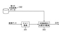
例えば、1回目のフラグ付加処理の回路を、図5に示すような構成とすることができる。1回目のフラグ付加処理は、フラグ置換値に置換する処理501を行い、ROM104から読み出した第1の欠陥画素データ502に基づき、欠陥画素の位置をフラグ値に置換する処理503を行う。
For example, the circuit for the first flag addition processing can be configured as shown in FIG. In the first flag addition process, a
さらに、2回目のフラグ付加処理の回路を、図6に示すような構成とすることができ、1回目のフラグ付加処理により出力される画像データを入力するようにする。1回目のフラグ付加処理で、もともとの画像データにあったフラグ値0と同じ値の画素は隣接した他の値に置換されているため、2回目のフラグ付加処理は処理501に相当する処理は必要ない。このため、2回目のフラグ付加処理では、ROM104から読み出した第2の欠陥画素データ601に基づいて欠陥画素の位置をフラグ値に置き換える処理602を行うのみでよい。このようにすることにより、2回目のフラグ付加処理が終了した時点で第1の欠陥画素に対応するフラグと第2の欠陥画素に対応するフラグとが付加された状態となる。
Furthermore, the circuit for the second flag addition process can be configured as shown in FIG. 6, and the image data output by the first flag addition process is input. In the first flag addition process, the pixel having the same value as the flag value 0 in the original image data is replaced with another adjacent value, so the second flag addition process corresponds to the
以上のように本実施形態によれば、1回目のフラグ付加処理を行う回路と2回目のフラグ付加処理を行う回路とをそれぞれ用意することにより、画像データを一旦メモリ等に格納させずに複数の欠陥画素データのマージと同等の効果を得ることが可能となる。 As described above, according to the present embodiment, by preparing a circuit that performs the first flag addition process and a circuit that performs the second flag addition process, a plurality of image data can be stored without being temporarily stored in a memory or the like. It is possible to obtain the same effect as the merging of defective pixel data.
(第3の実施形態)
以下、本実施形態について、図3および図4および図7を参照しながら説明する。大きな構成としては第1の実施形態と同様であるが、本実施形態では第1のフラグ付加処理の出力結果をもとに欠陥画素の検出を行い、検出結果に基づいて第2のフラグ付加処理をリアルタイムに行う。
(Third embodiment)
Hereinafter, the present embodiment will be described with reference to FIGS. 3, 4, and 7. The large configuration is the same as that of the first embodiment, but in this embodiment, defective pixels are detected based on the output result of the first flag addition process, and the second flag addition process is performed based on the detection result. In real time.
図7は、本実施形態に係る撮像装置700の構成例を示すブロック図である。
なお、第1の実施形態で説明した図1と同一の構成については、同じ符号を付しており、その構成の説明は省略する。なお、ROM104には、後述する欠陥画素検出部701により検出された欠陥画素データも記憶されるものとする。
FIG. 7 is a block diagram illustrating a configuration example of the
In addition, the same code | symbol is attached | subjected about the structure same as FIG. 1 demonstrated in 1st Embodiment, and description of the structure is abbreviate | omitted. Note that the
欠陥画素検出部701は、経時変化等で発生した欠陥画素を検出するためのものである。フラグ付加処理部702は、ROM104に予め記憶されている欠陥画素データと、欠陥画素検出部701で検出された欠陥画素データとをもとに、フラグを付加する。
The defective
次に、上記の構成における本実施形態の撮影動作について、図4を参照しながら説明する。
図4は、本実施形態に係る撮像装置700による撮影処理手順の一例を示すフローチャートである。本実施形態における1回目の欠陥画素のフラグ付加処理は、ROM104に格納されている製造工程時に検出された第1の欠陥画素データを読み出してフラグを付加するものであり、第1の実施形態で図3に示した例と同じである。
Next, the photographing operation of the present embodiment in the above configuration will be described with reference to FIG.
FIG. 4 is a flowchart illustrating an example of an imaging process procedure performed by the
まず、S201〜S206までの処理は、図2と同様であるため、説明は省略する。S203の判定の結果、2回目のフラグ付加処理である場合は、欠陥画素検出部701は、RAM105から画像データを読み出し、1回目のフラグ付加処理でフラグを付加した画像データに対して欠陥画素検出を行う(S401)。欠陥画素検出の方法としては、例えば、着目画素の画素値とその近傍画素の画素値とを比較し、着目画素との差分が閾値以内となる近傍画素が存在しなければ、着目画素を欠陥画素と判断することが考えられる。欠陥画素検出は、第1の欠陥画素データを補うものであり、リアルタイムに欠陥画素の検出を行うことによって、第1の欠陥画素データの作成後に発生した欠陥画素を検出する。また、欠陥画素検出が行われる画像データには、S205ですでに欠陥画素を示すフラグが付加されているため、例えば工場出荷時に検出されていた欠陥画素を回避しながら検出を行うことも可能である。つまり、S205ですでに欠陥画素を示すフラグが付加されている画素が着目画素の近傍に存在していた場合には、この画素を着目画素との比較対象から排除して、欠陥画素の検出を行えば良い。
First, the processing from S201 to S206 is the same as that in FIG. If the result of the determination in S203 is the second flag addition process, the defective
次に、フラグ付加処理部702は、欠陥画素であると検出された画素にフラグを付加する(S402)。この処理は第1の実施形態で図3に示した例と同じであるため、説明は省略する。このように、S402の処理を終えた時点で、第1の欠陥画素データとリアルタイムに欠陥画素検出された結果とがフラグとして付加されている。したがって、注目している画素の値が欠陥画素を意味する特定の値であるか否かを判定し、欠陥画素であった場合は欠陥画素補正を行い、有効な画素データを生成することができる。S210〜S212までの処理は、図2と同様であるため、説明は省略する。
Next, the flag
以上のように本実施形態によれば、予め検出されていた欠陥画素データとリアルタイムに検出された欠陥画素データといった複数の欠陥画素データがあった場合においても、フラグを順次付加していく。これにより、これらの欠陥画素データをマージしたものと同等の効果を得ることができ、簡単な構成で実現することが可能となる。なお、フラグ付加処理については、第2の実施形態と同様に、1回目のフラグ付加処理を行う構成を図5に示すような構成にし、2回目のフラグ付加処理を行う構成を図6に示す構成にしてもよい。 As described above, according to the present embodiment, flags are sequentially added even when there are a plurality of defective pixel data such as defective pixel data detected in advance and defective pixel data detected in real time. As a result, the same effects as those obtained by merging these defective pixel data can be obtained, and can be realized with a simple configuration. As for the flag addition processing, as in the second embodiment, the configuration for performing the first flag addition processing is as shown in FIG. 5, and the configuration for performing the second flag addition processing is shown in FIG. It may be configured.
(その他の実施形態)
また、本発明は、以下の処理を実行することによっても実現される。即ち、上述した実施形態の機能を実現するソフトウェア(プログラム)を、ネットワーク又は各種記憶媒体を介してシステム或いは装置に供給し、そのシステム或いは装置のコンピュータ(またはCPUやMPU等)がプログラムを読み出して実行する処理である。
(Other embodiments)
The present invention can also be realized by executing the following processing. That is, software (program) that realizes the functions of the above-described embodiments is supplied to a system or apparatus via a network or various storage media, and a computer (or CPU, MPU, or the like) of the system or apparatus reads the program. It is a process to be executed.
101 撮影レンズ
102 撮像素子
103 A/D変換器
104 ROM
105 RAM
106 フラグ付加処理部
107 欠陥画素補正部
108 DSP
109 ディスプレイ
110 記録媒体
101
105 RAM
106 Flag
109
Claims (8)
入力された画像データに対し、前記第1の欠陥画素データに対応した画素のフラグを特定の値に置換する第1のフラグ付加処理手段と、
前記第1のフラグ付加処理手段によってフラグが置換された画像データに対して、前記第2の欠陥画素データに対応した画素のフラグを前記特定の値に置換する第2のフラグ付加処理手段と、
前記第2のフラグ付加処理手段によってフラグが置換された画像データにおいて、フラグが前記特定の値である画素に対して欠陥画素補正を行う補正手段とを有することを特徴とする画像処理装置。 Storage means for storing first defective pixel data indicating position information of a defective pixel and second defective pixel data detected when the first defective pixel data is different from the first defective pixel data;
First flag addition processing means for replacing a flag of a pixel corresponding to the first defective pixel data with a specific value for the input image data;
Second flag addition processing means for replacing a flag of a pixel corresponding to the second defective pixel data with the specific value for the image data in which the flag is replaced by the first flag addition processing means;
An image processing apparatus comprising: correction means for performing defective pixel correction on a pixel whose flag is the specific value in the image data in which the flag is replaced by the second flag addition processing means.
入力された画像データに対し、前記第1の欠陥画素データに対応した画素のフラグを特定の値に置換する第1のフラグ付加処理手段と、
前記第1のフラグ付加処理手段によってフラグが置換された画像データに対して、前記第1の欠陥画素データとは異なる第2の欠陥画素データを検出する検出手段と、
前記第1のフラグ付加処理手段によってフラグが置換された画像データに対して、前記検出手段によって検出された第2の欠陥画素データに対応した画素のフラグを前記特定の値に置換する第2のフラグ付加処理手段と、
前記第2のフラグ付加処理手段によってフラグが置換された画像データにおいて、フラグが前記特定の値である画素に対して欠陥画素補正を行う補正手段とを有することを特徴とする画像処理装置。 Storage means for storing first defective pixel data indicating position information of the defective pixels;
First flag addition processing means for replacing a flag of a pixel corresponding to the first defective pixel data with a specific value for the input image data;
Detecting means for detecting second defective pixel data different from the first defective pixel data for the image data in which the flag is replaced by the first flag addition processing means;
A second flag that replaces the flag of the pixel corresponding to the second defective pixel data detected by the detection means with the specific value for the image data whose flag is replaced by the first flag addition processing means. Flag addition processing means;
An image processing apparatus comprising: correction means for performing defective pixel correction on a pixel whose flag is the specific value in the image data in which the flag is replaced by the second flag addition processing means.
入力された画像データに対し、前記第1の欠陥画素データに対応した画素のフラグを特定の値に置換する第1のフラグ付加処理工程と、
前記第1のフラグ付加処理工程においてフラグが置換された画像データに対して、前記第2の欠陥画素データに対応した画素のフラグを前記特定の値に置換する第2のフラグ付加処理工程と、
前記第2のフラグ付加処理工程においてフラグが置換された画像データにおいて、フラグが前記特定の値である画素に対して欠陥画素補正を行う補正工程とを有することを特徴とする画像処理方法。 An image processing method of an image processing apparatus for storing first defective pixel data indicating position information of a defective pixel and second defective pixel data detected when the first defective pixel data is different from the first defective pixel data,
A first flag addition processing step of replacing a flag of a pixel corresponding to the first defective pixel data with a specific value for the input image data;
A second flag addition processing step of replacing a pixel flag corresponding to the second defective pixel data with the specific value for the image data in which the flag is replaced in the first flag addition processing step;
An image processing method comprising: a correction step of performing defective pixel correction on a pixel whose flag is the specific value in the image data in which the flag is replaced in the second flag addition processing step.
入力された画像データに対し、前記第1の欠陥画素データに対応した画素のフラグを特定の値に置換する第1のフラグ付加処理工程と、
前記第1のフラグ付加処理工程においてフラグが置換された画像データに対して、前記第1の欠陥画素データとは異なる第2の欠陥画素データを検出する検出工程と、
前記第1のフラグ付加処理工程においてフラグが置換された画像データに対して、前記検出工程において検出された第2の欠陥画素データに対応した画素のフラグを前記特定の値に置換する第2のフラグ付加処理工程と、
前記第2のフラグ付加処理工程においてフラグが置換された画像データにおいて、フラグが前記特定の値である画素に対して欠陥画素補正を行う補正工程とを有することを特徴とする画像処理方法。 An image processing method of an image processing apparatus for storing first defective pixel data indicating position information of a defective pixel,
A first flag addition processing step of replacing a flag of a pixel corresponding to the first defective pixel data with a specific value for the input image data;
A detection step of detecting second defective pixel data different from the first defective pixel data for the image data in which the flag is replaced in the first flag addition processing step;
A second flag that replaces the flag of the pixel corresponding to the second defective pixel data detected in the detection step with the specific value for the image data in which the flag is replaced in the first flag addition processing step. A flag addition process,
An image processing method comprising: a correction step of performing defective pixel correction on a pixel whose flag is the specific value in the image data in which the flag is replaced in the second flag addition processing step.
入力された画像データに対し、前記第1の欠陥画素データに対応した画素のフラグを特定の値に置換する第1のフラグ付加処理工程と、
前記第1のフラグ付加処理工程においてフラグが置換された画像データに対して、前記第2の欠陥画素データに対応した画素のフラグを前記特定の値に置換する第2のフラグ付加処理工程と、
前記第2のフラグ付加処理工程においてフラグが置換された画像データにおいて、フラグが前記特定の値である画素に対して欠陥画素補正を行う補正工程とをコンピュータに実行させることを特徴とするプログラム。 A program for controlling an image processing apparatus that stores first defective pixel data indicating position information of a defective pixel and second defective pixel data detected when the first defective pixel data is different from the first defective pixel data. And
A first flag addition processing step of replacing a flag of a pixel corresponding to the first defective pixel data with a specific value for the input image data;
A second flag addition processing step of replacing a pixel flag corresponding to the second defective pixel data with the specific value for the image data in which the flag is replaced in the first flag addition processing step;
A program that causes a computer to execute a correction step of performing defective pixel correction on a pixel whose flag is the specific value in the image data in which the flag is replaced in the second flag addition processing step.
入力された画像データに対し、前記第1の欠陥画素データに対応した画素のフラグを特定の値に置換する第1のフラグ付加処理工程と、
前記第1のフラグ付加処理工程においてフラグが置換された画像データに対して、前記第1の欠陥画素データとは異なる第2の欠陥画素データを検出する検出工程と、
前記第1のフラグ付加処理工程においてフラグが置換された画像データに対して、前記検出工程において検出された第2の欠陥画素データに対応した画素のフラグを前記特定の値に置換する第2のフラグ付加処理工程と、
前記第2のフラグ付加処理工程においてフラグが置換された画像データにおいて、フラグが前記特定の値である画素に対して欠陥画素補正を行う補正工程とをコンピュータに実行させることを特徴とするプログラム。 A program for controlling an image processing apparatus that stores first defective pixel data indicating position information of a defective pixel,
A first flag addition processing step of replacing a flag of a pixel corresponding to the first defective pixel data with a specific value for the input image data;
A detection step of detecting second defective pixel data different from the first defective pixel data for the image data in which the flag is replaced in the first flag addition processing step;
A second flag that replaces the flag of the pixel corresponding to the second defective pixel data detected in the detection step with the specific value for the image data in which the flag is replaced in the first flag addition processing step. A flag addition process,
A program that causes a computer to execute a correction step of performing defective pixel correction on a pixel whose flag is the specific value in the image data in which the flag is replaced in the second flag addition processing step.
Priority Applications (1)
| Application Number | Priority Date | Filing Date | Title |
|---|---|---|---|
| JP2013060492A JP6218408B2 (en) | 2013-03-22 | 2013-03-22 | Image processing apparatus, image processing method, and program |
Applications Claiming Priority (1)
| Application Number | Priority Date | Filing Date | Title |
|---|---|---|---|
| JP2013060492A JP6218408B2 (en) | 2013-03-22 | 2013-03-22 | Image processing apparatus, image processing method, and program |
Publications (2)
| Publication Number | Publication Date |
|---|---|
| JP2014187516A JP2014187516A (en) | 2014-10-02 |
| JP6218408B2 true JP6218408B2 (en) | 2017-10-25 |
Family
ID=51834640
Family Applications (1)
| Application Number | Title | Priority Date | Filing Date |
|---|---|---|---|
| JP2013060492A Expired - Fee Related JP6218408B2 (en) | 2013-03-22 | 2013-03-22 | Image processing apparatus, image processing method, and program |
Country Status (1)
| Country | Link |
|---|---|
| JP (1) | JP6218408B2 (en) |
Families Citing this family (1)
| Publication number | Priority date | Publication date | Assignee | Title |
|---|---|---|---|---|
| JP2020088723A (en) | 2018-11-29 | 2020-06-04 | ソニーセミコンダクタソリューションズ株式会社 | Solid-state imaging element and imaging device |
Family Cites Families (4)
| Publication number | Priority date | Publication date | Assignee | Title |
|---|---|---|---|---|
| JPH0818873A (en) * | 1994-07-01 | 1996-01-19 | Hitachi Ltd | Video camera |
| JP4276817B2 (en) * | 2002-05-28 | 2009-06-10 | オリンパス株式会社 | Imaging device |
| JP2007295312A (en) * | 2006-04-25 | 2007-11-08 | Olympus Imaging Corp | Digital camera |
| JP2010021858A (en) * | 2008-07-11 | 2010-01-28 | Olympus Corp | Pixel defect correction device |
-
2013
- 2013-03-22 JP JP2013060492A patent/JP6218408B2/en not_active Expired - Fee Related
Also Published As
| Publication number | Publication date |
|---|---|
| JP2014187516A (en) | 2014-10-02 |
Similar Documents
| Publication | Publication Date | Title |
|---|---|---|
| US9721609B2 (en) | Image capturing apparatus, image capturing system, and control method for the image capturing apparatus | |
| US8970742B2 (en) | Image processing apparatus and method capable of performing correction process speedily and easily | |
| JP2011040893A (en) | Device for correcting defective pixel data, imaging device, and method of correcting defective pixel data | |
| JP5084366B2 (en) | IMAGING DEVICE AND IMAGING DEVICE CONTROL METHOD | |
| JP6261397B2 (en) | Imaging apparatus and control method thereof | |
| JP2007174266A (en) | Imaging apparatus | |
| JP5996418B2 (en) | Imaging apparatus and imaging method | |
| JP6218408B2 (en) | Image processing apparatus, image processing method, and program | |
| JP5410158B2 (en) | Imaging system and electronic information device | |
| JP6091229B2 (en) | Imaging apparatus, control method thereof, and program | |
| JP2007306506A (en) | Imaging apparatus | |
| JP2005341244A (en) | Imaging device, defective pixel detecting method, and program | |
| JP2007228269A (en) | Image signal processing device and method | |
| JP2010050730A (en) | Imaging apparatus and defect correction apparatus | |
| JP5968145B2 (en) | Image processing apparatus and control method thereof | |
| US11729506B2 (en) | Imaging element with processor configured to receive vibration information, imaging apparatus, operation method of imaging element, and program | |
| JP2012124800A (en) | Imaging apparatus | |
| JP2009239935A (en) | Image photographing device and image photographing method, and computer program | |
| JP4498253B2 (en) | Image processing device | |
| JP2018026743A (en) | Image processor, control method, and program | |
| JP2015061137A (en) | Imaging apparatus, control method of the same, and program | |
| US20110267498A1 (en) | Image pickup apparatus and control method therefor | |
| JP6324130B2 (en) | Imaging device | |
| JP2006157192A (en) | Defective pixel correction apparatus and defective pixel correction method | |
| JP2009111801A (en) | Image processor |
Legal Events
| Date | Code | Title | Description |
|---|---|---|---|
| A621 | Written request for application examination |
Free format text: JAPANESE INTERMEDIATE CODE: A621 Effective date: 20160317 |
|
| A977 | Report on retrieval |
Free format text: JAPANESE INTERMEDIATE CODE: A971007 Effective date: 20161216 |
|
| A131 | Notification of reasons for refusal |
Free format text: JAPANESE INTERMEDIATE CODE: A131 Effective date: 20170131 |
|
| A521 | Request for written amendment filed |
Free format text: JAPANESE INTERMEDIATE CODE: A523 Effective date: 20170323 |
|
| TRDD | Decision of grant or rejection written | ||
| A01 | Written decision to grant a patent or to grant a registration (utility model) |
Free format text: JAPANESE INTERMEDIATE CODE: A01 Effective date: 20170829 |
|
| A61 | First payment of annual fees (during grant procedure) |
Free format text: JAPANESE INTERMEDIATE CODE: A61 Effective date: 20170926 |
|
| R151 | Written notification of patent or utility model registration |
Ref document number: 6218408 Country of ref document: JP Free format text: JAPANESE INTERMEDIATE CODE: R151 |
|
| LAPS | Cancellation because of no payment of annual fees |