JP5016547B2 - Contact device for providing electrical contact between flat conductive line elements - Google Patents
Contact device for providing electrical contact between flat conductive line elements Download PDFInfo
- Publication number
- JP5016547B2 JP5016547B2 JP2008116501A JP2008116501A JP5016547B2 JP 5016547 B2 JP5016547 B2 JP 5016547B2 JP 2008116501 A JP2008116501 A JP 2008116501A JP 2008116501 A JP2008116501 A JP 2008116501A JP 5016547 B2 JP5016547 B2 JP 5016547B2
- Authority
- JP
- Japan
- Prior art keywords
- contact
- bus bar
- side wall
- contact device
- bus
- Prior art date
- Legal status (The legal status is an assumption and is not a legal conclusion. Google has not performed a legal analysis and makes no representation as to the accuracy of the status listed.)
- Active
Links
Images


Classifications
-
- H—ELECTRICITY
- H01—ELECTRIC ELEMENTS
- H01R—ELECTRICALLY-CONDUCTIVE CONNECTIONS; STRUCTURAL ASSOCIATIONS OF A PLURALITY OF MUTUALLY-INSULATED ELECTRICAL CONNECTING ELEMENTS; COUPLING DEVICES; CURRENT COLLECTORS
- H01R4/00—Electrically-conductive connections between two or more conductive members in direct contact, i.e. touching one another; Means for effecting or maintaining such contact; Electrically-conductive connections having two or more spaced connecting locations for conductors and using contact members penetrating insulation
- H01R4/28—Clamped connections, spring connections
- H01R4/48—Clamped connections, spring connections utilising a spring, clip, or other resilient member
- H01R4/4881—Clamped connections, spring connections utilising a spring, clip, or other resilient member using a louver type spring
-
- H—ELECTRICITY
- H01—ELECTRIC ELEMENTS
- H01R—ELECTRICALLY-CONDUCTIVE CONNECTIONS; STRUCTURAL ASSOCIATIONS OF A PLURALITY OF MUTUALLY-INSULATED ELECTRICAL CONNECTING ELEMENTS; COUPLING DEVICES; CURRENT COLLECTORS
- H01R25/00—Coupling parts adapted for simultaneous co-operation with two or more identical counterparts, e.g. for distributing energy to two or more circuits
- H01R25/14—Rails or bus-bars constructed so that the counterparts can be connected thereto at any point along their length
Abstract
Description
本発明は、平坦な導電ライン要素、特に母線間に電気的接触を与える接触装置に関する。 The present invention relates to a contact device for providing electrical contact between flat conductive line elements, in particular busbars.
平坦な導電ライン要素間に電気的接触を与える幾つかの装置は先行技術より知られている。 Several devices for providing electrical contact between flat conductive line elements are known from the prior art.
例えば、欧州特許第0568755号明細書(特許文献1)は、オーバラップ母線または平坦プレート間に電気的接触を与える接触装置を開示している。この接触装置は、第1母線と第2母線との間に配置され、且つ前記母線間配置されている幾つかの接触モジュールを備えている。その第1母線はネジおよびナットにより第2母線に結合されている。 For example, European Patent No. 0568755 discloses a contact device that provides electrical contact between overlapping bus bars or flat plates. The contact device includes several contact modules arranged between the first bus bar and the second bus bar and arranged between the bus bars. The first bus bar is coupled to the second bus bar by screws and nuts.
母線間の電気的接触を与える更なる装置は、米国特許第4174143号明細書(特許文献2)に開示されている。幾つかの、U字形状をした部材が複数の母線を受け入れるため平行に配置されている。そのU字形状をした部材は同一直線上配置された第1と第2の母線を受け入れる2つの開口を備えている。 A further device for providing electrical contact between the busbars is disclosed in U.S. Pat. No. 4,174,143. Several U-shaped members are arranged in parallel to receive a plurality of busbars. The U-shaped member has two openings for receiving first and second busbars arranged on the same straight line.
母線内を流れる電流は、多かれ少なかれ、母線に対し平行であり、母線の幅全体わたり均一に分布している。しかしながら、前記ネジおよびナットの領域において電流の流れは、横断面減少とネジの存在により集中される。そうした電流とインダクタンス効果の集中は磁気的損失の原因となる。特に、高周波の電流ではそうした損失は否定的な影響を与える。 The current flowing in the busbar is more or less parallel to the busbar and is evenly distributed over the entire width of the busbar. However, in the area of the screw and nut, the current flow is concentrated due to the reduced cross section and the presence of the screw. Such concentration of current and inductance effect causes magnetic loss. In particular, such losses have a negative effect on high-frequency currents.
本発明の目的は、先行技術装置の難点を有しない、母線のような平坦な導電ライン要素間に電気的接触を与えるための接触装置を提供することにある。特に、そうした接触装置では接触ゾーンにおける磁気的損失を最小にするものである。 It is an object of the present invention to provide a contact device for providing electrical contact between flat conductive line elements, such as busbars, that does not have the disadvantages of prior art devices. In particular, such contact devices minimize magnetic losses in the contact zone.
この目的は、請求項1に記載の特徴をもつ接触装置により達成される。したがって、実質的に互いに平行に配置された第1および第2の母線間に電気的接触を与える接触装置は、実質的に平行に伸びる2つの側壁を有するホルダからなり、その側壁は前記第2の母線を受け入れるスロットを取り囲むようになっている。前記側壁は、スロットに面する内側の面と外側の面とからなる。1つの側壁では、第1の母線が外側の面と対面し、第2の母線が内側の面と対面するように適合されている。前記側壁は、当該側壁を介し内側の面から外側の面への、すなわち、第1および第2の母線間に電気的接触を与える接触要素からなる。
This object is achieved by a contact device having the features of
ネジを使用せず、電流が伝達される一定の横断面を有する場合は、磁気的損失は顕著に減少可能である。さらに、そうした接触装置は追加的な工具や装置を用いることなく極めて容易に母線に取付けることが可能である。したがって、本発明による接触装置は母線上に極めて容易に挟むことが可能である。 Without using screws and having a constant cross-section through which current is transmitted, the magnetic losses can be significantly reduced. Furthermore, such contact devices can be attached to the busbars very easily without the use of additional tools or devices. Therefore, the contact device according to the present invention can be very easily sandwiched on the bus bar.
好適には、その接触要素は、前記少なくとも1つの側壁の内側の面の上部および内側の面を超えて、および/または、外側の面の上部および外側の面を超えて突出している。すなわち、前記接触要素はスロットの中へおよび外側の面を超えて伸びている。 Preferably, the contact element projects beyond the upper and inner surfaces of the inner surface of the at least one side wall and / or beyond the upper and outer surfaces of the outer surface. That is, the contact element extends into the slot and beyond the outer surface.
接触要素の突出により、接触装置は前記母線間での確実で信頼性ある結合を達成可能である。 Due to the protrusion of the contact element, the contact device can achieve a reliable and reliable connection between the busbars.
好適には、その接触要素は、内側の面の上部および内側の面を超えて、および/または、外側の面の上部および外側の面を超えて突出している弾力性を有し可動の接触部材からなる。前記接触部材が実際に母線に接触すると、当該母線の表面は、通常、外側または内側の側壁の表面に接触する。したがって、接触部材は、母線が接触している状態では、必ずしも内側の面および/または、外側の面を超えて伸びている必要はない。しかしながら、非接触状態、すなわち、母線への接触がないときには、前記接触部材は通常、内側の面および/または、外側の面を超えて伸びている。 Preferably, the contact element is a resiliently movable contact member protruding beyond the upper and inner surfaces of the inner surface and / or beyond the upper and outer surfaces of the outer surface. Consists of. When the contact member actually contacts the bus bar, the surface of the bus bar usually contacts the surface of the outer or inner side wall. Therefore, the contact member does not necessarily have to extend beyond the inner surface and / or the outer surface in a state where the bus bar is in contact. However, in a non-contact state, i.e., when there is no contact with the busbar, the contact member typically extends beyond the inner surface and / or the outer surface.
前記弾力性のある部材は母線に対し力を作用し、電気的結合の信頼性を向上させる。 The elastic member applies a force to the bus bar and improves the reliability of electrical coupling.
好適には、前記ホルダは、電気的絶縁性であり、前記接触要素に適応した手段からなる。好適には、そのホルダはプラスチックまたは、繊維強化プラスチックで作られる。その中でも、ポリエチレン、ポリアミド、ポリエーテル・エーテル・ケトン(PEEK)、またはポリオキシメチレン(POM)は適合するプラスチックである。 Preferably, the holder is electrically insulating and comprises means adapted to the contact element. Preferably, the holder is made of plastic or fiber reinforced plastic. Among them, polyethylene, polyamide, polyether ether ketone (PEEK), or polyoxymethylene (POM) are suitable plastics.
好適には、前記接触要素に適応した手段は、接触要素を受け入れるための溝を有する断面が長方形の開口である。 Preferably, the means adapted to the contact element is an opening having a rectangular cross section with a groove for receiving the contact element.
好適には、前記接触要素は、互いに、本質的に平行配置された数多くの、分離されている同一のバネを取付けた個々の要素からなる。前記バネを取付けた個々の要素はキャリアバンドに固定されている。好適には、前記個々の要素は、絡み合った接触ブリッジである。前記キャリアバンドは前記キャリアバンドから横向きに伸びる案内ブラケットを備えている。好適には、長方形開口の溝は、前記案内ブラケットの少なくとも部分または接触要素の他の部分を受け入れることが可能である。 Preferably, the contact element consists of a number of individual elements fitted with a number of separate identical springs arranged essentially parallel to each other. The individual elements to which the springs are attached are fixed to a carrier band. Preferably, the individual elements are intertwined contact bridges. The carrier band includes a guide bracket extending laterally from the carrier band. Preferably, the rectangular opening groove is capable of receiving at least part of the guide bracket or other part of the contact element.
本発明のさらなる実施例は従属請求項によって表わされる。 Further embodiments of the invention are represented by the dependent claims.
図面を参照して可能な実施例を説明する。図面およびその記載は好適な実施例を例示するものであり、特許請求の範囲により定義した発明を限定して解釈されるべきではない。 Possible embodiments will be described with reference to the drawings. The drawings and the description are only for the purpose of illustrating preferred embodiments and are not to be construed as limiting the invention as defined by the appended claims.
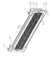
図1は、斜視図の本発明による第1の母線および第2の母線(図示せず)間に電気的接触を与える接触装置を示す。典型的には、前記第1および第2の母線は互いに、実質的に平行である。しかしながら、母線という用語は平坦な導電ライン要素を含むものとする。典型的には、そのような母線は厚さが1mmと10mmとの間で、幅が25mmと200mmの間にある。その横断面は好適には長方形である。 FIG. 1 shows a contact device for providing electrical contact between a first bus bar and a second bus bar (not shown) according to the invention in perspective view. Typically, the first and second bus bars are substantially parallel to each other. However, the term bus bar is intended to include flat conductive line elements. Typically, such bus bars are between 1 mm and 10 mm thick and between 25 mm and 200 mm wide. Its cross section is preferably rectangular.
本発明による接触装置は、前記母線間の電気的接触を与えるための接触要素1とその電気的接触要素1に適合するホルダ2からなる。
The contact device according to the invention comprises a
その接触要素1は、図4または5だけでなく図1に示される。その接触要素1は、数多くの、分離されている同一のバネを取付けた個々の要素10からなり、これらはまた、絡み合った接触ブリッジとして指定することも可能である。接触ブリッジ10は互いに、本質的に平行に配置される。キャリアバンド11は長手方向の軸に沿って伸びており、また接触ブリッジ10はキャリアバンド11に固定されている。案内ブラケット12はキャリアバンド11の横向きに伸びている。
The
第1実施例で、接触ブリッジ10はキャリアバンド11に直接取付けることが可能であり、その中で、接触ブリッジ10の部分は少なくとも部分的にキャリアバンド11を包含または取り囲んでいる。
In the first embodiment, the
それに代わる第2の実施例では、接触ブリッジ10が少なくとも部分的に案内ブラケット12を包含するように、それら2つの端部に形成ゾーン13を備えている。好適には、この包含は、案内ブラケットがさらに案内するため自由端14を備えるようにキャリアバンド11の近傍領域にある。案内ブラケット12の包含により、接触ブリッジ10の幾つかの部分はキャリアバンド11の下方または上方に伸びている。
In an alternative second embodiment, the forming
キャリアバンド11の両側、すなわち、上方および下方での接触ブリッジ10が伸張しているということは、接触ブリッジ10の部分がキャリアバンド11を超えて突出しているので、電気的接触が接触ブリッジ10それ自身により与えられることが可能であるという長所を有する。それ故に、キャリアバンド11は、接触ブリッジ10用キャリアの役目を果たすためそこにある。さらに、前記キャリアバンド11と案内ブラケット12はまた、接触ブリッジ10用のバネまたはねじり要素として作用する。したがって、接触ブリッジ10は、母線との接触後それらの原位置に復帰させようとする弾力を受ける。
The extension of the
そのような接触要素1は欧州特許第1119077号明細書から公知である。ここでは、欧州特許第1119077号公報による技術的教示は参照することで本願に取り込まれる。同様な特徴や機能を持つ他の公知の接触要素もまた使用することが可能である。
Such a
しかしながら、他の実施例において、接触要素1のキャリアバンド11はまた、電気的伝達要素として使用することが可能である。そのような要素は、例えば米国特許第3895853号公報に開示されている。
However, in other embodiments, the
ホルダ2は2つの側壁21、22からなる。そのいずれも、同一方向で実質的にブリッジ要素24と平行に伸びている。側壁21、22はスロット23を取り囲む。換言すると、スロット23は側壁21、22によって与えられている。スロット23は、母線、好適には第2の母線を受け入れるため配置される。好適には、ホルダ2はプラスチックまたは繊維強化プラスチックのような電気的に絶縁性の材料で作られる。その中でも、ポリエチレン、ポリアミド、ポリエーテル・エーテル・ケトン(PEEK)、またはポリオキシメチレン(POM)は適合するプラスチックである。
The
側壁21、22はスロット23に対面する内側の面211、221を有する。したがって、その内側の面211、221はスロット23に配置されている第2の母線の表面と対面し接触している。スロット23内に母線がない場合は、内側の面211、221は直接対面することとなる。
The
さらに、側壁21、22は、外側の面212、222を有する。前記外側の面212、222は、前記内側の面211、221の反対側にある、側壁21、22の当該側面に配置される。外側の面212は、第1の母線によって接触されることが可能である。このことは、本発明による接触装置が母線アセンブリ内に位置していない場合、前記外側の面212がスロット23内に位置していない前記第1の母線と対面するということを意味している。外側の面212、221は、母線アセンブリの絶縁性キャリア2を保持するために設けられている。
Further, the
図1による実施例において、接触要素1は、側壁21内に配置されている。前記側壁はまた、接触側壁として指定することが可能である。他の電気的接触要素のない側壁22は、クリップ側壁またはクリップ要素として形成される。好適には、接触要素1を有する側壁21は、接触要素1を有しない側壁22よりも長い。接触要素を有する側壁21は屈曲性のある接触要素を備えるように、また、当該接触要素の屈曲性や弾力性を消耗させる最小限の寸法またはギャップ下での屈曲性接触による圧縮を回避するように、設計される。
In the embodiment according to FIG. 1, the
ホルダ2は、単一物品または、図5で説明されるように幾つかの単一物品のグループのいずれかとして設けられることが可能である。好適には、ホルダ2は射出型成形法を利用可能なようにプラスチックから作られる。代替的または追加的に、機械加工を使用することも可能である。完成したホルダ2が単一物品として設けられる場合、射出型成形法を用いることが可能であり、そこでは接触要素1がプラスチックの射出前に型の中に配置されることが可能である。
The
接触要素1はホルダ2により包含されているので接触要素1は機械的な影響に対しホルダ2によって保護される。
Since the
図2は、本発明による接触装置の側面図を示す。接触要素1の接触ブリッジ10は、接触側壁21の外側の面212を超えその面の上方に突出している。接触ブリッジ10が母線に接触すると、前記接触ブリッジ10は接触側壁21の方向で外側の面212に向けて屈曲される。しかしながら、また、前記側壁21内の接触要素1を逆方向に、すなわち、接触ブリッジ10が内側の面211を超えその面の上方に突出するよう配置することも可能である。好適には、接触要素1である接触ブリッジ10の傾斜部のような幾つかの部分のみが、それぞれ前記外側の面212または内側の面211を超えその面の上方に突出する。
FIG. 2 shows a side view of a contact device according to the present invention. The
クリップ要素22は、その内側の面221にカムまたは膨らみ223を設けている。その膨らみ223は円柱状に形成され、内側の面221からスロット23の中へ伸びている。したがって、それはスロット23の幅を減少させる。スロット23の幅Xは、スロット23の方向から見たときスロット23の最小隙間として定義される。好適には、前記幅Xはスロット23により受け入れられる母線の幅よりも小さい。このことは、取付けた状態でクリップ面からの力が母線上に作用し、それ故に、例えば、振動によりそれ自身緩むことがないので特に有利である。膨らみ223は本発明による接触装置が母線上で滑るのを回避する。スロット23の幅Xは、容易に母線の幅に適合することが可能である。
The
クリップ要素22または側壁22は、ブリッジ要素24を介して接触要素1を有する側壁21に結合される。好適には、前記ブリッジ要素24は弾力性をもつかまたは弾性的に屈曲性を有する。弾力特性により、クリップ要素22と側壁21はその内側の面に垂直な方向の力を与える。一旦、母線がスロット23に配置されると、前記の力は保持力を与える。しかしながら、他の実施例では、クリップ要素22自身が弾力特性を持つようにすることも可能である。好適には、クリップ要素22は、ブリッジ要素24から見たとき接触要素1を有する側壁21よりも短い。しかしながら、他の実施例では、クリップ要素22は、側壁21よりも長いか等しい。
本実施例では、2つのクリップ要素22が配置されている。前記クリップ要素は接触要素1を有する側壁21の長さよりも短い長さを有する。他の実施例では、前記クリップ要素は、接触要素1を有する側壁21の全長を超えて伸びている。しかしながら、2つ以上のクリップ要素22または、接触要素1を有する側壁21の長さよりも短い長さを有する1つのクリップ要素21を設けることもまた可能である。
In this embodiment, two
図3は、本発明による接触装置の平面図を示す。接触要素1はホルダ2の長方形開口25に配置されているので、接触要素1はホルダ2により完全に囲まれている。
FIG. 3 shows a plan view of a contact device according to the present invention. Since the
見てわかるように、ホルダ2は長さLと幅Wを有する。長さLは好適には、20mmと500mmの間にある。幅Wは好適には、20mmと150mmの間にある。長方形開口25は長さL1と幅W1を有する。好適には、長さL1は15mmと480mmの間にある。幅Wは、好適には、10mmと130mmの間にある。好適には、ホルダ2内に配置された接触要素1は長方形開口25の表面全体を超えて伸びている。このことは、外側(すなわち、長方形開口を介して)から見える接触要素の部分が長方形開口25の表面全体を超えて伸びており、したがって、接触要素1は全長L1を超え、さらに全幅W1を超えて伸びていることを意味する。接触装置の長さがその用途、例えば伝達される電流に適応可能なようにその長さが可変であるということは、本発明の有利な点である。
As can be seen, the
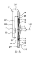
図4は、本発明による接触装置の図3に示されるA−A線断面に沿う断面図を示す。この図において、その場合の側壁の1つである側壁21は、内側の面211から外側の面212への電気的接触を接触要素1によって与えることが可能であるということは明瞭である。
FIG. 4 shows a cross-sectional view of the contact device according to the present invention along the line AA shown in FIG. In this figure, it is clear that the
A−Aの横断面図において、接触要素1がホルダ2内に適合していることが示される。長方形開口25は、その長い方のエッジに沿って伸びる溝26からなる。前記溝26はキャリアバンド11の部分を適合させることを可能にする。特に、前記溝26は案内ブラケット12または、接触要素1の案内ブラケット12の自由端を受け入れる。好適には、案内ブラケット12の最外側の部分だけが溝26の中へ伸びている。しかしながら、代替的実施例では、溝26を有する長方形開口25の短い方のエッジを与えることも同様に可能である。
In the cross-sectional view AA, it is shown that the
同様に、その断面図において、接触要素1の部分が、側壁21の内側の面211および/または、外側の面212を超えて突出している。その実施例では、接触ブリッジ10、すなわち、接触ブリッジ10の傾斜部分が外側の面212を超えて突出し、そして形成ゾーン13が内側の面211を超えて突出している。接触要素1が逆に配置される場合は、接触ブリッジ10が内側の面211を超えて突出し、そして形成ゾーン13が外側の面212を超えて突出する。
Similarly, in that cross-sectional view, the part of the
図5は、図3のB−B線断面に沿って取られた横断面を示す。この実施例では、クリップ要素22とブリッジ要素24は一体に形成されている。このことは、クリップ要素22とブリッジ要素24が、クリップ片7として示すことのできる1つの単一物品であるということを意味する。その結果として、接触要素1からなる側壁21もまた単一物品である。クリップ片7は、ラッチ結合27によって接触要素1を有する側壁21に結合されることが可能である。好適には、2つのクリップ片7は、接触要素1を有する側壁21の両側に配置される。このことは、クリップ片7が、機械的ストッパまたは溝26に配置された接触要素1用の橋脚としてだけでなく、クリップ要素22とブリッジ要素24の役割をも果たすということを意味する。
FIG. 5 shows a cross section taken along the line BB in FIG. In this embodiment, the
図4および5による横断面において、人はさらに、接触要素からなる側壁21によって電気的接触が与えられるということを認識できる。接触ブリッジ10が、母線と接触して同母線が前記側壁の外側に面するように配置されているときには、その接触ブリッジ10は外側の面212の方向で且つ外側の面212に向けて移動される。これは矢視100で示される。それによって、接触ブリッジ10は、外側の面212に面する母線の表面に接触する。
In the cross section according to FIGS. 4 and 5, the person can further recognize that electrical contact is provided by the
キャリアバンド11の下方、すなわち、内側の面211の方向に伸びている接触ブリッジ10の部分が、内側の面211を超えて突出している。母線がスロット23に配置されている場合には、接触ブリッジ10の前記部分と母線との間に電気的接触が成立する。
A portion of the
このことは、接触要素1、特に接触ブリッジ10が、接触要素1からなる側壁21の外側の面212に配置された第1の母線とスロット23に配置された第2の母線との間で電気的接触の役目を果たすことを意味する。換言すれば、電気的接触は、側壁21を介し、外側の面212から内側の面211へ、またはその逆へと与えられる。
This means that the
本発明によるそうした接触装置では、2つの母線間の結合による磁気的損失は先行技術から知られる接触装置、例えば電気的接触を与えるネジを用いる装置に関し25%まで減少されることが可能である。 In such a contact device according to the invention, the magnetic loss due to the coupling between the two busbars can be reduced to 25% for contact devices known from the prior art, for example devices using screws that provide electrical contact.
図6は、結合状態における双極性母線の配置の斜視図を示し、そして図7は、非結合状態における前記配置の斜視図を示す。前記母線は本発明による接触装置によって結合される。しかしながら、接触装置はまた、単極性母線の配置用として利用することも可能である。 FIG. 6 shows a perspective view of the arrangement of the bipolar busbars in the coupled state and FIG. 7 shows a perspective view of the arrangement in the uncoupled state. Said bus bars are joined by a contact device according to the invention. However, the contact device can also be used for placement of unipolar busbars.
双極性母線の配置は、異なる電圧の電流を伝達するため4つの母線からなる。第1の母線3と第2の母線4は接触装置C1により結合される。第3の母線5と第4の母線6は接触装置C2により結合される。好適には、母線3、4、5、6の全ては、互いに実質的に平行な接触領域に伸びている。特に、第1の接触装置C1または第2の接触装置C2のいずれかにより結合されるこれら母線は互いに実質的に平行に伸びている。このことは本実施例において、第1の母線3は第2の母線4と実質的に平行であり、第3の母線5は第4の母線6と実質的に平行であることを意味する。
The arrangement of bipolar buses consists of four buses for transmitting currents of different voltages. The first bus bar 3 and the
第3の母線5および第4の母線6だけでなく第1の母線3および第2の母線4は、互いに、第1の母線3と第2の母線4との間、または、第3の母線5と第4の母線6との間にそれぞれギャップがあるように配置される。それにより、前記ギャップは、接触装置C1またはC2の接触要素1を有する側壁21を前記ギャップの中に配置可能な幅を有する。
Not only the
図面から分かるように、第2の母線4は第1の接触装置C1のスロット23内へ伸びている。それによって、その母線は内側の面211、221に対面し、そして接触要素1の部分に接触する。したがって、接触要素1と第2の母線4との間の電気的接触が成立する。第1の接触装置C1は、接触要素1を有する側壁21が第1の母線3に対面するように配置される。このことは、外側の面212が第1の母線3に対面するということを意味する。
As can be seen from the drawing, the
図面から分かるように、第1の母線3は第2の母線4に関して移動可能である。これは矢視101により例示される。第2の母線4に関して第1の母線3が移動すると、第1の母線3は接触要素1の接触ブリッジ10に突き当たる。前記接触ブリッジ10は前記移動方向に対し角度または傾斜して配置されているので、前記接触ブリッジ10は、接触要素1を有する側壁21の外側の面212に向けて変位する。接触ブリッジ10第1の母線3表面に当接すると直ちに接触要素1と第1の母線3との間の電気的接触が成立する。すでに接触要素1と第2の母線4との間の電気的接触があるので、第1の母線は接触要素1を介して第2の母線4に電気的に結合される。換言すれば、接触要素1を側壁21に配置することにより、第1の母線3と第2の母線4間に配置された側壁21を介して電気的接触が与えられる。
As can be seen from the drawing, the first bus bar 3 is movable with respect to the
第3の母線5を第4の母線6に結合するため上述したと同様な方法が適用可能である。
In order to couple the
この実施例では、第1の母線3および第3の母線5は、第2の母線4および第4の母線6に関して移動可能である。このことは、接触装置C1、C2が第2の母線4および第4の母線6上に配置されることを意味する。代替的には、静止した母線を有することもまた可能であり、さらに、母線間に電気的接触を与えるため挿入可能な接触装置とすることも可能である。
In this embodiment, the first bus bar 3 and the
図6および7から分かるように、第1の母線3および第3の母線5は、互いに平行に配置されている。絶縁層8が第1の母線3および第2の母線4の間に配置されている。さらに、絶縁層9が第2の母線4および第4の母線6の間に配置されている。
As can be seen from FIGS. 6 and 7, the first bus bar 3 and the
単極性の母線が配置される場合、母線の一対を省略することが可能である。 When unipolar busbars are arranged, a pair of busbars can be omitted.
図示していないさらなる実施例では、ホルダの中に2以上の接触要素を配置することが可能である。 In a further embodiment not shown, it is possible to arrange two or more contact elements in the holder.
本発明による接触装置を有する第1の母線および第2の母線間に電気的接触を与える方法は、接触要素1を有する側壁21が第1の母線および第2の母線間に位置付けされるように母線に関して接触装置を正しい方向に置き、本発明による接触装置のスロット23が前記第2の母線4を受け入れる、すなわち、第2の母線4上で接触装置をシフトするように、第2の母線4の上に接触装置を配置し、接触要素1が第1の母線3の表面に接触するように、本発明による接触装置に向けて第1の母線を移動する、ステップからなる。
The method for providing electrical contact between a first bus bar and a second bus bar with a contact device according to the invention is such that the
第2の母線4に関して第1の母線3が移動しない場合には、最後のステップは必要ない。
If the first bus 3 does not move with respect to the
第1の母線および第2の母線間の電気的接触が妨げられる場合は、上記の方法は逆の手順にて適用することが可能である。 If electrical contact between the first bus bar and the second bus bar is prevented, the above method can be applied in the reverse procedure.
1 接触要素
2 ホルダ
3 第1の母線
4 第2の母線
5 第3の母線
6 第4の母線
7 クリップ片
8 絶縁層
9 絶縁層
10 接触ブリッジ
11 キャリアバンド
12 案内ブラケット
13 形成ゾーン
14 自由端
21 側壁/接触側壁
22 側壁/クリップ要素
23 スロット
24 ブリッジ要素
25 長方形開口
26 溝
27 ラッチ結合
211 内側の面
212 外側の面
213 長方形開口
221 内側の面
222 外側の面
DESCRIPTION OF
Claims (15)
Applications Claiming Priority (2)
| Application Number | Priority Date | Filing Date | Title |
|---|---|---|---|
| EP07405128A EP1986272B1 (en) | 2007-04-26 | 2007-04-26 | Contact device for providing an electrical contact between flat current carrying line elements |
| EP07405128.5 | 2007-04-26 |
Publications (2)
| Publication Number | Publication Date |
|---|---|
| JP2008277299A JP2008277299A (en) | 2008-11-13 |
| JP5016547B2 true JP5016547B2 (en) | 2012-09-05 |
Family
ID=38162146
Family Applications (1)
| Application Number | Title | Priority Date | Filing Date |
|---|---|---|---|
| JP2008116501A Active JP5016547B2 (en) | 2007-04-26 | 2008-04-26 | Contact device for providing electrical contact between flat conductive line elements |
Country Status (8)
| Country | Link |
|---|---|
| US (1) | US7678995B2 (en) |
| EP (1) | EP1986272B1 (en) |
| JP (1) | JP5016547B2 (en) |
| KR (1) | KR101433797B1 (en) |
| CN (1) | CN101295821B (en) |
| AT (1) | ATE520172T1 (en) |
| CA (1) | CA2629994C (en) |
| ES (1) | ES2370849T3 (en) |
Families Citing this family (12)
| Publication number | Priority date | Publication date | Assignee | Title |
|---|---|---|---|---|
| DE202010008933U1 (en) * | 2010-11-02 | 2010-12-23 | Sma Solar Technology Ag | Electrical connection between two busbars of planar conductors and an insulating layer arranged between the conductors |
| JP2016512918A (en) * | 2013-03-18 | 2016-05-09 | マルチ−ホールディング アーゲー | Contact element |
| CN103208692A (en) * | 2013-03-25 | 2013-07-17 | 上海电巴新能源科技有限公司 | Conductive pole column |
| DE102014100421B3 (en) * | 2014-01-15 | 2015-01-15 | Maschinenfabrik Reinhausen Gmbh | Switch for a switching device with switching shaft, its use in a diverter switch, switching device with switching shaft and switch, their use in an on-load tap-changer, load switch for on-load tap-changer and control transformer |
| US9190791B1 (en) | 2014-07-31 | 2015-11-17 | Power Distribution, Inc. | Electrical busway splice connector |
| US9520703B2 (en) | 2014-07-31 | 2016-12-13 | Power Distribution, Inc. | Electrical busway splice connector |
| DE102015216632A1 (en) * | 2015-08-31 | 2017-03-02 | Te Connectivity Germany Gmbh | Arrangement for establishing an electrical connection between a flat contact and a high-current conductor |
| KR102342616B1 (en) * | 2016-07-18 | 2021-12-23 | 스타우블리 일렉트리컬 커넥털스 아게 | connection element |
| DE102018124583A1 (en) * | 2017-10-19 | 2019-04-25 | Phoenix Contact Gmbh & Co. Kg | Terminal arrangement with a busbar |
| WO2022236450A1 (en) * | 2021-05-08 | 2022-11-17 | 舍弗勒技术股份两合公司 | Current busbar assembly and assembly method therefor, and current transmission device |
| WO2023051763A1 (en) * | 2021-10-01 | 2023-04-06 | 长春捷翼汽车零部件有限公司 | Flat-belt type connecting mechanism, electric energy transmission apparatus, and motor vehicle |
| EP4195419A1 (en) * | 2021-12-09 | 2023-06-14 | ABB E-mobility B.V. | Electric connector for high power charging |
Family Cites Families (16)
| Publication number | Priority date | Publication date | Assignee | Title |
|---|---|---|---|---|
| JPS4730135Y1 (en) * | 1969-07-15 | 1972-09-08 | ||
| DE2243034C2 (en) | 1972-09-01 | 1974-09-19 | Multi-Contact Ag, Basel (Schweiz) | Electrical contact arrangement |
| US4013329A (en) * | 1976-02-23 | 1977-03-22 | Multilam Corporation | Multiple plate assembly for forming electrical connector or switch |
| US4174143A (en) | 1976-03-29 | 1979-11-13 | Cutler-Hammer, Inc. | Bus duct joint employing lightly-loaded multiple-point electrical connector |
| JPS53133785A (en) * | 1977-04-26 | 1978-11-21 | Hitachi Cable Ltd | Bus bar conductor connection adapter |
| US5029254A (en) * | 1990-03-23 | 1991-07-02 | Instrument Specialties Company, Inc. | Clip mounted electromagnetic shielding device |
| EP0568755B1 (en) * | 1992-05-08 | 1996-08-21 | Multi-Contact Ag | Contact device |
| US5435743A (en) * | 1994-03-17 | 1995-07-25 | Chrysler Corporation | Casing for assuring an electrical connection |
| JPH0817528A (en) * | 1994-06-27 | 1996-01-19 | Oki Densen Kk | Relay connector for flexible base and rigid base |
| US5588884A (en) * | 1995-09-08 | 1996-12-31 | Packard Hughes Interconnect Company | Stamped and formed contacts for a power connector |
| US6365297B1 (en) * | 1999-12-15 | 2002-04-02 | Delphi Technologies, Inc. | High-power bussing connection system for a battery pack |
| CH694478A5 (en) | 2000-01-20 | 2005-01-31 | Multi Holding Ag | Contact element. |
| US6485337B2 (en) * | 2000-08-30 | 2002-11-26 | Delphi Technologies, Inc. | Electrical connector |
| JP4596638B2 (en) | 2000-12-22 | 2010-12-08 | タイコエレクトロニクスジャパン合同会社 | Electrical connector |
| EP1523069A1 (en) * | 2003-10-10 | 2005-04-13 | Hirschmann Electronics GmbH & Co. KG | Contact spring for an antenna amplifier |
| DE102004018492B3 (en) | 2004-04-14 | 2006-02-09 | Yazaki Europe Ltd., Hemel Hempstead | Socket for electrically conductive connection with a plug pin, in particular flat pin |
-
2007
- 2007-04-26 AT AT07405128T patent/ATE520172T1/en not_active IP Right Cessation
- 2007-04-26 EP EP07405128A patent/EP1986272B1/en active Active
- 2007-04-26 ES ES07405128T patent/ES2370849T3/en active Active
-
2008
- 2008-04-25 CA CA2629994A patent/CA2629994C/en active Active
- 2008-04-25 CN CN2008100940717A patent/CN101295821B/en active Active
- 2008-04-25 KR KR1020080038669A patent/KR101433797B1/en active IP Right Grant
- 2008-04-26 JP JP2008116501A patent/JP5016547B2/en active Active
- 2008-04-28 US US12/111,086 patent/US7678995B2/en not_active Expired - Fee Related
Also Published As
| Publication number | Publication date |
|---|---|
| ATE520172T1 (en) | 2011-08-15 |
| US20080271921A1 (en) | 2008-11-06 |
| CA2629994A1 (en) | 2008-10-26 |
| KR20080096450A (en) | 2008-10-30 |
| CN101295821A (en) | 2008-10-29 |
| EP1986272A1 (en) | 2008-10-29 |
| ES2370849T3 (en) | 2011-12-23 |
| EP1986272B1 (en) | 2011-08-10 |
| US7678995B2 (en) | 2010-03-16 |
| JP2008277299A (en) | 2008-11-13 |
| CN101295821B (en) | 2012-12-05 |
| CA2629994C (en) | 2015-06-30 |
| KR101433797B1 (en) | 2014-08-25 |
Similar Documents
| Publication | Publication Date | Title |
|---|---|---|
| JP5016547B2 (en) | Contact device for providing electrical contact between flat conductive line elements | |
| US9461373B2 (en) | Terminal clamp | |
| EP2824767B1 (en) | Busbar connection system for use with a power distribution system, and Electrical device including the bubar connection system | |
| CN110277677B (en) | Socket with improved structure | |
| KR20070009678A (en) | Power conduction chain | |
| KR20090025338A (en) | Articulated element for a power supply chain | |
| KR101652383B1 (en) | Connector | |
| US11290000B2 (en) | Switch module assembly, and method for manufacturing the same | |
| US8870580B2 (en) | Connector with connecting members held by a beam supported by a supporting member | |
| CN111009762B (en) | Jumper for electric terminal | |
| JPS60172186A (en) | Plug type connector | |
| EP0403206A2 (en) | Contact equipped with a bypass element | |
| CA2241719C (en) | Improved roller slide device | |
| FI96909B (en) | Key | |
| EP3051562A1 (en) | Spring Member for an Electric Switching Device such as a Cradle Relay | |
| KR20220065036A (en) | Electrical connector and test conduction device | |
| JP6131252B2 (en) | Contact terminal | |
| US11417971B2 (en) | Assembly element for an actuator | |
| EP0951030A3 (en) | Electric contact with twin-knife insertion coupling, particularly for disconnectors, switches or the like. | |
| DE50206873D1 (en) | Electrical connector for data technology | |
| KR200342711Y1 (en) | A joint bar | |
| KR101555689B1 (en) | Busbar Connecting Device for Distributing Electric Power | |
| DE50301847D1 (en) | Contact arrangement for an electrical switching device | |
| JP2002178800A (en) | Connecting structure of feeder wire | |
| SE411273B (en) | ELECTROMAGNETICALLY MANUFACTURED ELECTRICAL COUPLER |
Legal Events
| Date | Code | Title | Description |
|---|---|---|---|
| A621 | Written request for application examination |
Free format text: JAPANESE INTERMEDIATE CODE: A621 Effective date: 20110328 |
|
| A977 | Report on retrieval |
Free format text: JAPANESE INTERMEDIATE CODE: A971007 Effective date: 20120511 |
|
| TRDD | Decision of grant or rejection written | ||
| A01 | Written decision to grant a patent or to grant a registration (utility model) |
Free format text: JAPANESE INTERMEDIATE CODE: A01 Effective date: 20120525 |
|
| A01 | Written decision to grant a patent or to grant a registration (utility model) |
Free format text: JAPANESE INTERMEDIATE CODE: A01 |
|
| A61 | First payment of annual fees (during grant procedure) |
Free format text: JAPANESE INTERMEDIATE CODE: A61 Effective date: 20120608 |
|
| FPAY | Renewal fee payment (event date is renewal date of database) |
Free format text: PAYMENT UNTIL: 20150615 Year of fee payment: 3 |
|
| R150 | Certificate of patent or registration of utility model |
Ref document number: 5016547 Country of ref document: JP Free format text: JAPANESE INTERMEDIATE CODE: R150 Free format text: JAPANESE INTERMEDIATE CODE: R150 |
|
| R250 | Receipt of annual fees |
Free format text: JAPANESE INTERMEDIATE CODE: R250 |
|
| R250 | Receipt of annual fees |
Free format text: JAPANESE INTERMEDIATE CODE: R250 |
|
| R250 | Receipt of annual fees |
Free format text: JAPANESE INTERMEDIATE CODE: R250 |
|
| S111 | Request for change of ownership or part of ownership |
Free format text: JAPANESE INTERMEDIATE CODE: R313111 |
|
| R360 | Written notification for declining of transfer of rights |
Free format text: JAPANESE INTERMEDIATE CODE: R360 |
|
| R370 | Written measure of declining of transfer procedure |
Free format text: JAPANESE INTERMEDIATE CODE: R370 |
|
| S111 | Request for change of ownership or part of ownership |
Free format text: JAPANESE INTERMEDIATE CODE: R313111 |
|
| R350 | Written notification of registration of transfer |
Free format text: JAPANESE INTERMEDIATE CODE: R350 |
|
| R250 | Receipt of annual fees |
Free format text: JAPANESE INTERMEDIATE CODE: R250 |
|
| R250 | Receipt of annual fees |
Free format text: JAPANESE INTERMEDIATE CODE: R250 |
|
| R250 | Receipt of annual fees |
Free format text: JAPANESE INTERMEDIATE CODE: R250 |
|
| R250 | Receipt of annual fees |
Free format text: JAPANESE INTERMEDIATE CODE: R250 |
|
| R250 | Receipt of annual fees |
Free format text: JAPANESE INTERMEDIATE CODE: R250 |
|
| R250 | Receipt of annual fees |
Free format text: JAPANESE INTERMEDIATE CODE: R250 |