JP5011631B2 - Semiconductor manufacturing apparatus and semiconductor manufacturing system - Google Patents
Semiconductor manufacturing apparatus and semiconductor manufacturing system Download PDFInfo
- Publication number
- JP5011631B2 JP5011631B2 JP2004163892A JP2004163892A JP5011631B2 JP 5011631 B2 JP5011631 B2 JP 5011631B2 JP 2004163892 A JP2004163892 A JP 2004163892A JP 2004163892 A JP2004163892 A JP 2004163892A JP 5011631 B2 JP5011631 B2 JP 5011631B2
- Authority
- JP
- Japan
- Prior art keywords
- gas
- gas flow
- vertical blowing
- supply means
- semiconductor manufacturing
- Prior art date
- Legal status (The legal status is an assumption and is not a legal conclusion. Google has not performed a legal analysis and makes no representation as to the accuracy of the status listed.)
- Active
Links
Images


Classifications
-
- C—CHEMISTRY; METALLURGY
- C23—COATING METALLIC MATERIAL; COATING MATERIAL WITH METALLIC MATERIAL; CHEMICAL SURFACE TREATMENT; DIFFUSION TREATMENT OF METALLIC MATERIAL; COATING BY VACUUM EVAPORATION, BY SPUTTERING, BY ION IMPLANTATION OR BY CHEMICAL VAPOUR DEPOSITION, IN GENERAL; INHIBITING CORROSION OF METALLIC MATERIAL OR INCRUSTATION IN GENERAL
- C23C—COATING METALLIC MATERIAL; COATING MATERIAL WITH METALLIC MATERIAL; SURFACE TREATMENT OF METALLIC MATERIAL BY DIFFUSION INTO THE SURFACE, BY CHEMICAL CONVERSION OR SUBSTITUTION; COATING BY VACUUM EVAPORATION, BY SPUTTERING, BY ION IMPLANTATION OR BY CHEMICAL VAPOUR DEPOSITION, IN GENERAL
- C23C16/00—Chemical coating by decomposition of gaseous compounds, without leaving reaction products of surface material in the coating, i.e. chemical vapour deposition [CVD] processes
- C23C16/44—Chemical coating by decomposition of gaseous compounds, without leaving reaction products of surface material in the coating, i.e. chemical vapour deposition [CVD] processes characterised by the method of coating
- C23C16/50—Chemical coating by decomposition of gaseous compounds, without leaving reaction products of surface material in the coating, i.e. chemical vapour deposition [CVD] processes characterised by the method of coating using electric discharges
- C23C16/517—Chemical coating by decomposition of gaseous compounds, without leaving reaction products of surface material in the coating, i.e. chemical vapour deposition [CVD] processes characterised by the method of coating using electric discharges using a combination of discharges covered by two or more of groups C23C16/503 - C23C16/515
-
- C—CHEMISTRY; METALLURGY
- C23—COATING METALLIC MATERIAL; COATING MATERIAL WITH METALLIC MATERIAL; CHEMICAL SURFACE TREATMENT; DIFFUSION TREATMENT OF METALLIC MATERIAL; COATING BY VACUUM EVAPORATION, BY SPUTTERING, BY ION IMPLANTATION OR BY CHEMICAL VAPOUR DEPOSITION, IN GENERAL; INHIBITING CORROSION OF METALLIC MATERIAL OR INCRUSTATION IN GENERAL
- C23C—COATING METALLIC MATERIAL; COATING MATERIAL WITH METALLIC MATERIAL; SURFACE TREATMENT OF METALLIC MATERIAL BY DIFFUSION INTO THE SURFACE, BY CHEMICAL CONVERSION OR SUBSTITUTION; COATING BY VACUUM EVAPORATION, BY SPUTTERING, BY ION IMPLANTATION OR BY CHEMICAL VAPOUR DEPOSITION, IN GENERAL
- C23C16/00—Chemical coating by decomposition of gaseous compounds, without leaving reaction products of surface material in the coating, i.e. chemical vapour deposition [CVD] processes
- C23C16/22—Chemical coating by decomposition of gaseous compounds, without leaving reaction products of surface material in the coating, i.e. chemical vapour deposition [CVD] processes characterised by the deposition of inorganic material, other than metallic material
- C23C16/30—Deposition of compounds, mixtures or solid solutions, e.g. borides, carbides, nitrides
- C23C16/301—AIII BV compounds, where A is Al, Ga, In or Tl and B is N, P, As, Sb or Bi
- C23C16/303—Nitrides
Description
本発明は、基板に半導体薄膜を形成するための半導体製造装置およびこの半導体製造装置を用いた半導体製造システムに関する。 The present invention relates to a semiconductor manufacturing apparatus for forming a semiconductor thin film on a substrate and a semiconductor manufacturing system using the semiconductor manufacturing apparatus.
青色および紫外光領域の光電デバイスの応用材料として、ワイドバンドギャップを有するAlN、AlGaN、GaN、GaInN、InN等のIII[IUPAC(国際純粋及び応用化学連合)の1989年無機化学命名法改訂版による族番号は13]−V[同改訂版による族番号は15]族化合物半導体が注目されている。
現在、薄膜を成長させる方法として主に分子線エピタキシー(MBE)法や有機金属気相成長(MOCVD)法が用いられている。このうち、MOCVD法は気相で輸送された原料で化学反応を起こして、生成した半導体を基板上に堆積させる方法であり、成膜時に供給するガスの流量を制御することで極薄膜形成や混晶比の制御を容易に行うことができる。また、原理的には大面積の基板に均一に結晶を成長させることが可能であることからMOCVD法は工業的に重要な方法である。
As an application material for photoelectric devices in the blue and ultraviolet light regions, III [IUPAC (International Union of Pure and Applied Chemistry)] 1989 Inorganic Chemical Nomenclature Revision The group number is 13] -V [the group number according to the revised version is 15].
Currently, molecular beam epitaxy (MBE) and metal organic chemical vapor deposition (MOCVD) are mainly used as methods for growing thin films. Among these, the MOCVD method is a method of causing a chemical reaction with the raw material transported in the gas phase and depositing the generated semiconductor on the substrate. By controlling the flow rate of the gas supplied during film formation, The mixed crystal ratio can be easily controlled. In principle, the MOCVD method is an industrially important method because crystals can be uniformly grown on a large-area substrate.
しかし、MOCVD法において高品質なGaN結晶の成長に必要とされる基板温度は900から1200℃と高温であり、これにより基板に使用される材料が制限される。また、電極上に半導体を積層するため、デバイス構成を作製する上での自由度に限界がある。これに対し、原料ガスをマイクロ波や高周波によるプラズマ発振によって分解し、さらにそのリモートプラズマ中に気体状の有機金属化合物を導入し、生成された半導体を基板上に堆積させるリモートプラズマMOCVD法は成長温度を下げる上で有効な手段である。 However, the substrate temperature required for the growth of high-quality GaN crystals in the MOCVD method is as high as 900 to 1200 ° C., which limits the materials used for the substrate. In addition, since a semiconductor is stacked on an electrode, there is a limit to the degree of freedom in manufacturing a device configuration. On the other hand, the remote plasma MOCVD method, in which the source gas is decomposed by microwave or high frequency plasma oscillation, a gaseous organometallic compound is introduced into the remote plasma, and the generated semiconductor is deposited on the substrate is grown. This is an effective means for lowering the temperature.
このリモートプラズマMOCVD法において、混晶や多層膜を作製する上で問題となるキャリアガスの種類、圧力、ガス流量などの因子を独立に制御するために、複数のプラズマ発生手段を設けた製造装置による成膜も行われている。複数のプラズマ発生手段を用意し、一方から補助材料として水素などを導入することで、水素ラジカルによる還元効果により炭素の半導体膜中への混入が減少でき、膜欠陥を抑え、高品質の薄膜を作製することができる。 In this remote plasma MOCVD method, a manufacturing apparatus provided with a plurality of plasma generating means for independently controlling factors such as the type of carrier gas, pressure, and gas flow rate, which are problems in producing mixed crystals and multilayer films The film formation by is also performed. By preparing multiple plasma generation means and introducing hydrogen or the like as an auxiliary material from one side, the reduction effect of hydrogen radicals can reduce the incorporation of carbon into the semiconductor film, suppress film defects, and produce high-quality thin films. Can be produced.
しかし、従来の複数のプラズマ発生手段を用いた半導体製造装置では、各プラズマ発生手段が基板成膜面と垂直な方向に対して別方向に位置するように配置されていた(特許文献1参照)。このため、活性化されたそれぞれのガスが基板成膜面と垂直な方向に対して異なる方向から反応容器内に進入し、それぞれのプラズマ発生手段により活性化されたガスの流量の違いによって、反応容器内のガスの流れが変化し、基板成膜面上の位置によって膜厚が異なってしまう。このため、成膜面内の膜厚を均一にするために、基板の回転機構を設けるなど複雑な装置を必要とした。 However, in a conventional semiconductor manufacturing apparatus using a plurality of plasma generating means, each plasma generating means is arranged to be located in a different direction with respect to a direction perpendicular to the substrate film forming surface (see Patent Document 1). . For this reason, each activated gas enters the reaction vessel from a different direction with respect to the direction perpendicular to the substrate deposition surface, and the reaction is caused by the difference in the flow rate of the gas activated by each plasma generating means. The gas flow in the container changes, and the film thickness varies depending on the position on the substrate deposition surface. For this reason, in order to make the film thickness in the film formation surface uniform, a complicated apparatus such as a substrate rotation mechanism is required.
また、各プラズマ発生手段により活性化された原料ガス(第1の原料ガス)に、この原料ガスと反応する原料ガス(第2の原料ガス)を導入して成膜する場合、第2の原料ガスがプラズマ発生手段により異なり、かつ、各プラズマ発生手段により活性化された各々の反応ガスを基板成膜面の直上付近で混合する場合には、反応ガスの混合が十分に行われず、基板上に成長する薄膜の組成が成膜面内の位置によって異なってしまう。このような面内組成ムラは、基板を回転させる回転機構を設けても必ずしも回避できない。
以上のようなことから最適化された条件で成長する部分は基板上の僅かな領域に限られ、大面積の基板上に組成および膜厚が均一な膜を形成できなかった。
In addition, in the case of forming a film by introducing a source gas (second source gas) that reacts with the source gas into the source gas (first source gas) activated by each plasma generating means, the second source material When the gas differs depending on the plasma generation means and each reaction gas activated by each plasma generation means is mixed in the vicinity immediately above the substrate film formation surface, the reaction gas is not sufficiently mixed, The composition of the thin film that grows varies depending on the position in the film formation surface. Such in-plane composition unevenness cannot necessarily be avoided even if a rotation mechanism for rotating the substrate is provided.
As described above, a portion that grows under optimized conditions is limited to a small area on the substrate, and a film having a uniform composition and film thickness cannot be formed on a large-area substrate.
このような問題を解決するために、プラズマ発生手段により活性化されたガスが、基板成膜面に対して略垂直に吹き付けるように構成された半導体製造装置が提案されている(特許文献2参照)。しかし、この半導体製造装置では、大面積の半導体薄膜を形成する場合、面内の膜厚均一性については品質要求に十分に対応できるものの、面内の組成均一性については不充分な場合があり、面内の組成均一性のより厳しい品質要求には対応できない場合があった。
本発明は、上記問題点を解決することを課題とする。すなわち、本発明は、基板の回転機構などの複雑な構造を用いることなく、大面積の基板上に組成および膜厚が均一な半導体薄膜を形成するための半導体製造装置およびこれを用いた半導体製造システムを提供することを課題とする。 An object of the present invention is to solve the above problems. That is, the present invention relates to a semiconductor manufacturing apparatus for forming a semiconductor thin film having a uniform composition and film thickness on a large-area substrate without using a complicated structure such as a substrate rotation mechanism, and semiconductor manufacturing using the same. The problem is to provide a system.
本発明者らは、上記課題を達成するために、プラズマ発生手段により活性化されたガスが基板成膜面に対して略垂直に吹き付けるように構成された半導体製造装置において、面内の膜質が不均一になる問題点について鋭意検討した。
まず、面内の膜質が不均一になる理由としては種々考えられるが、基板の成膜面に到達する直前のガス流の成膜面と平行な方向の活性化状態の不均一性が一因として考えられる。
In order to achieve the above object, the inventors of the present invention provide a semiconductor manufacturing apparatus configured such that the gas activated by the plasma generating means is sprayed substantially perpendicularly to the substrate film forming surface. We have intensively studied the problem of non-uniformity.
First, there are various reasons why the in-plane film quality is non-uniform, but this is partly due to the non-uniformity of the activation state in the direction parallel to the film-forming surface of the gas flow just before reaching the film-forming surface of the substrate. Is considered.
一方、特許文献2に示される半導体製造装置では、プラズマ発生手段により活性化されたガスが基板成膜面に対して略垂直に吹き付けるガス流(垂直吹き付けガス流)に対して放電する他のプラズマ発生手段(垂直吹き付けガス流放電手段)の放電方向が、垂直吹き付けガス流の流れ方向と同じ方向である上に、この垂直吹き付けガス流放電手段の放電部は、基板成膜面に対向する平面の一部分を占めるように設けられている。
On the other hand, in the semiconductor manufacturing apparatus disclosed in
このため、本発明者らは、垂直吹き付けガス流の中心に放電が十分に届かず膜質が不均一になるものと考えた。また、ガス流中心に放電が十分に届くように放電部を設けようとすると、この放電部自体が垂直吹き付けガス流の流れを阻害してしまうことになる。
さらに、垂直吹き付けガス流放電手段は、垂直吹き付けガス流の主流部内に位置するように設けられているため、垂直吹き付けガス流放電手段に生成物が付着・堆積し、この生成物が脱落することによって、反応容器内や基板成膜面を汚染してしまう場合もある。このような汚染を防ぐためには、頻繁に反応容器内を清掃しなければならないことに加え、半導体装置を用いて連続生産を行う場合には、清掃メンテナンスや清掃メンテナンス後の立ち上げのような生産に直接寄与しない時間が増大し、生産性が低下してしまう場合もある。
For this reason, the present inventors considered that the discharge did not sufficiently reach the center of the vertical blowing gas flow and the film quality became non-uniform. Further, if the discharge part is provided so that the discharge reaches the center of the gas flow sufficiently, the discharge part itself obstructs the flow of the vertical blowing gas flow.
Further, since the vertical blowing gas flow discharge means is provided so as to be located in the main flow portion of the vertical blowing gas flow, the product adheres to and accumulates on the vertical blowing gas flow discharge means, and this product falls off. In some cases, the inside of the reaction container or the substrate film formation surface may be contaminated. In order to prevent such contamination, the inside of the reaction vessel must be frequently cleaned. In addition, when performing continuous production using semiconductor devices, production such as cleaning maintenance and startup after cleaning maintenance is performed. In some cases, the time not directly contributing to the process time increases and the productivity decreases.
従って、本発明者らは、垂直吹き付けガス流を基板成膜面方向に均一に活性化できる位置にプラズマ発生手段を設けることが重要であると考えた。これに加えて、汚染防止の観点からは、垂直吹き付けガス流の流れを阻害しない位置にプラズマ発生手段を設けることも重要であると考え、以下の本発明を見出した。すなわち、本発明は、 Therefore, the present inventors considered that it is important to provide the plasma generating means at a position where the vertical blowing gas flow can be uniformly activated in the direction of the substrate film forming surface. In addition to this, from the viewpoint of preventing contamination, it is considered important to provide a plasma generating means at a position that does not hinder the flow of the vertical blowing gas flow, and the following present invention has been found. That is, the present invention
<1>
反応容器と、基板を保持する基板ホルダーと、前記反応容器内に原料ガスおよび補助ガスを供給するための複数のガス供給手段と、該ガス供給手段から前記基板の一方の面である成膜面方向へと流れるガスを活性化するように配置された複数のプラズマ発生手段と、を備え、
少なくとも1つ以上のプラズマ発生手段により活性化されたガスが、前記成膜面に対して略垂直に吹き付ける垂直吹き付けガス流が形成される半導体製造装置において、
前記複数のプラズマ発生手段として、V族元素を含む第1の原料ガスを活性化する第1のプラズマ発生手段と、
該第1のプラズマ発生手段および前記複数のガス供給手段よりも前記垂直吹き付けガス流のガス流れ方向下流側に設けられ前記垂直吹き付けガス流のガス流れ方向中心に向かってプラズマ放電を行い、前記ガスを活性化する垂直吹き付けガス流活性化用プラズマ発生手段とを設け、
前記複数のガス供給手段として、前記第1の原料ガスを供給し前記反応容器内に前記垂直吹き付けガス流を形成する第1のガス供給手段と、
該第1のガス供給手段よりも前記垂直吹き付けガス流のガス流れ方向下流側であり且つ前記垂直吹き付けガス流活性化用プラズマ発生手段よりも前記垂直吹き付けガス流のガス流れ方向上流側に設けられ前記第1の原料ガスとは異なるIII族元素を含む第2の原料ガスを前記垂直吹き付けガス流に合流するように供給する第2のガス供給手段と、
前記第1のガス供給手段よりも前記垂直吹き付けガス流のガス流れ方向下流側であり且つ前記垂直吹き付けガス流活性化用プラズマ発生手段よりも前記垂直吹き付けガス流のガス流れ方向上流側に設けられ前記垂直吹き付けガス流に合流するように補助ガスを供給する第3のガス供給手段とを設けたことを特徴とする半導体製造装置である。
<1>
A reaction vessel, a substrate holder for holding a substrate, a plurality of gas supply means for supplying a raw material gas and the auxiliary gas, in one surface of the substrate from the gas supply means is in said reaction vessel A plurality of plasma generating means arranged to activate the gas flowing in the direction of the film formation surface,
In a semiconductor manufacturing apparatus in which a gas flow activated by at least one or more plasma generating means is blown substantially perpendicularly to the film-forming surface is formed.
A first plasma generating means for activating a first source gas containing a group V element as the plurality of plasma generating means;
The plasma is discharged toward the center in the gas flow direction of the vertical blowing gas flow provided downstream of the first plasma generating means and the plurality of gas supply means in the gas flow direction of the vertical blowing gas flow, and the gas And a plasma generating means for activating the vertical blowing gas flow for activating
As the plurality of gas supply means, a first gas supply means for supplying the first source gas and forming the vertical blowing gas flow in the reaction vessel;
Provided downstream of the first gas supply means in the gas flow direction of the vertical blowing gas flow and upstream of the vertical blowing gas flow activation plasma generation means in the gas flow direction of the vertical blowing gas flow. A second gas supply means for supplying a second source gas containing a group III element different from the first source gas so as to merge with the vertical blowing gas stream;
Provided downstream of the first gas supply means in the gas flow direction of the vertical blowing gas flow and upstream of the vertical blowing gas flow activation plasma generation means in the gas flow direction of the vertical blowing gas flow. A semiconductor manufacturing apparatus comprising a third gas supply means for supplying an auxiliary gas so as to merge with the vertical blowing gas flow.
<2>
前記垂直吹き付けガス流活性化用プラズマ発生手段が、少なくとも前記垂直吹き付けガス流の主流部から離れた位置に設置されることを特徴とする<1>に記載の半導体製造装置である。
<2>
The vertical blowing gas stream activating plasma generating means is a semiconductor manufacturing apparatus according to <1>, characterized in that installed in a position away from the main portion of at least the vertical blowing gas stream.
<3>
前記垂直吹き付けガス流活性化用プラズマ発生手段が、前記垂直吹き付けガス流の主流部を囲み、且つ、放電面が前記垂直吹き付けガス流のガス流れ方向と略平行に配置された円筒状電極であることを特徴とする<2>に記載の半導体製造装置である。
<3>
The plasma generating means for activating the vertical blowing gas flow is a cylindrical electrode that surrounds the main flow portion of the vertical blowing gas flow and has a discharge surface disposed substantially parallel to the gas flow direction of the vertical blowing gas flow. <2> The semiconductor manufacturing apparatus according to <2>.
<4>
前記第1のガス供給手段及び前記第2のガス供給手段の少なくとも一方が、流量調整器を1つ以上含むことを特徴とする<1>に記載の半導体製造装置である。
< 4 >
At least one of the first gas supply means and said second gas supply means is a semiconductor manufacturing apparatus according to the flow regulator to <1>, which comprises one or more.
<5>
反応容器と、基板を保持する基板ホルダーと、前記反応容器内に原料ガスおよび補助ガスを供給するための複数のガス供給手段と、該ガス供給手段から前記基板の一方の面である成膜面方向へと流れるガスを活性化するように配置された複数のプラズマ発生手段と、を備え、
少なくとも1つ以上のプラズマ発生手段により活性化されたガスが、前記成膜面に対して略垂直に吹き付ける垂直吹き付けガス流が形成され、
前記複数のプラズマ発生手段として、V族元素を含む第1の原料ガスを活性化する第1のプラズマ発生手段と、
該第1のプラズマ発生手段および前記複数のガス供給手段よりも前記垂直吹き付けガス流のガス流れ方向下流側に設けられ前記垂直吹き付けガス流のガス流れ方向中心に向かってプラズマ放電を行い、前記ガスを活性化する垂直吹き付けガス流活性化用プラズマ発生手段とを設け、
前記複数のガス供給手段として、前記第1の原料ガスを供給し前記反応容器内に前記垂直吹き付けガス流を形成する第1のガス供給手段と、
該第1のガス供給手段よりも前記垂直吹き付けガス流のガス流れ方向下流側であり且つ前記垂直吹き付けガス流活性化用プラズマ発生手段よりも前記垂直吹き付けガス流のガス流れ方向上流側に設けられ前記第1の原料ガスとは異なるIII族元素を含む第2の原料ガスを前記垂直吹き付けガス流に合流するように供給する第2のガス供給手段と、
前記第1のガス供給手段よりも前記垂直吹き付けガス流のガス流れ方向下流側であり且つ前記垂直吹き付けガス流活性化用プラズマ発生手段よりも前記垂直吹き付けガス流のガス流れ方向上流側に設けられ前記垂直吹き付けガス流に合流するように補助ガスを供給する第3のガス供給手段とを設けた半導体製造装置を2つ以上含む半導体製造システムであって、
前記基板が、大気雰囲気と遮断された状態でいずれか1つの半導体製造装置の反応容器から他の半導体製造装置の反応容器へと移動可能な基板搬送手段を備えたことを特徴とする半導体製造システムである。
<5>
A reaction vessel, a substrate holder for holding a substrate, a plurality of gas supply means for supplying a raw material gas and the auxiliary gas, in one surface of the substrate from the gas supply means is in said reaction vessel A plurality of plasma generating means arranged to activate the gas flowing in the direction of the film formation surface,
A gas stream activated by at least one or more plasma generating means is formed so as to blow substantially perpendicularly to the film-forming surface;
A first plasma generating means for activating a first source gas containing a group V element as the plurality of plasma generating means;
The plasma is discharged toward the center in the gas flow direction of the vertical blowing gas flow provided downstream of the first plasma generating means and the plurality of gas supply means in the gas flow direction of the vertical blowing gas flow, and the gas And a plasma generating means for activating the vertical blowing gas flow for activating
As the plurality of gas supply means, a first gas supply means for supplying the first source gas and forming the vertical blowing gas flow in the reaction vessel;
Provided downstream of the first gas supply means in the gas flow direction of the vertical blowing gas flow and upstream of the vertical blowing gas flow activation plasma generation means in the gas flow direction of the vertical blowing gas flow. A second gas supply means for supplying a second source gas containing a group III element different from the first source gas so as to merge with the vertical blowing gas stream;
Provided downstream of the first gas supply means in the gas flow direction of the vertical blowing gas flow and upstream of the vertical blowing gas flow activation plasma generation means in the gas flow direction of the vertical blowing gas flow. A semiconductor manufacturing system including two or more semiconductor manufacturing apparatuses provided with a third gas supply means for supplying an auxiliary gas so as to join the vertical blowing gas flow,
A semiconductor manufacturing system comprising a substrate transfer means that is movable from a reaction vessel of any one semiconductor manufacturing apparatus to a reaction container of another semiconductor manufacturing apparatus in a state where the substrate is cut off from the atmospheric air It is.
以上に説明したように本発明によれば、基板の回転機構などの複雑な構造を用いることなく、大面積の基板上に組成および膜厚が均一な半導体薄膜を形成するための半導体製造装置およびこれを用いた半導体製造システムを提供することができる。 As described above, according to the present invention, a semiconductor manufacturing apparatus for forming a semiconductor thin film having a uniform composition and film thickness on a large-area substrate without using a complicated structure such as a substrate rotation mechanism, and the like. A semiconductor manufacturing system using this can be provided.
(半導体製造装置)
本発明の半導体製造装置は、反応容器と、基板を保持する基板ホルダーと、前記反応容器内に原料ガスおよび/または補助ガスを供給するための複数のガス供給手段と、該ガス供給手段から前記基板の一方の面である成膜面方向へと流れるガスを活性化するように配置された複数のプラズマ発生手段と、を備え、少なくとも1つ以上のプラズマ発生手段により活性化されたガスが、前記成膜面に対して略垂直に吹き付ける垂直吹き付けガス流が形成される半導体製造装置において、前記垂直吹き付けガス流のガス流れ方向中心に向かってプラズマ放電を行い、前記ガスを活性化する垂直吹き付けガス流活性化用プラズマ発生手段を少なくとも1つ設けたことを特徴とする。
(Semiconductor manufacturing equipment)
The semiconductor manufacturing apparatus of the present invention includes a reaction vessel, a substrate holder for holding a substrate, a plurality of gas supply means for supplying a source gas and / or an auxiliary gas into the reaction vessel, and the gas supply means from the gas supply means. and a plurality of plasma generating means arranged to activate the gas flow to the deposition surface direction is one surface of the substrate, the gas is activated by at least one plasma generating means In a semiconductor manufacturing apparatus in which a vertical blowing gas flow that blows substantially perpendicularly to the film forming surface is formed, a vertical discharge that activates the gas by performing plasma discharge toward the center of the vertical blowing gas flow in the gas flow direction. At least one plasma generating means for activating the blowing gas flow is provided.
従って、本発明の半導体装置を用いれば、基板の回転機構などの複雑な構造を用いることなく、大面積の基板上に組成および膜厚が均一な半導体薄膜を形成することができる。
また、本発明の半導体製造装置に設けられる垂直吹き付けガス流活性化用プラズマ発生手段は、垂直吹き付けガス流のガス流れ方向中心に向かってプラズマ放電を行い、前記ガスを活性化するため、基板の成膜面に到達する直前のガス流の成膜面と平行な方向の活性化状態を、従来の垂直吹き付けガス流活性化用プラズマ発生手段を備えた半導体製造装置よりもより均一にでき、成膜面内の組成均一性を更に向上させることができる。
Therefore, by using the semiconductor device of the present invention, a semiconductor thin film having a uniform composition and film thickness can be formed on a large-area substrate without using a complicated structure such as a substrate rotation mechanism.
The plasma generating means for activating the vertical blowing gas flow provided in the semiconductor manufacturing apparatus of the present invention performs plasma discharge toward the center of the vertical blowing gas flow in the gas flow direction to activate the gas . The activation state of the gas flow immediately before reaching the film formation surface in the direction parallel to the film formation surface can be made more uniform than the conventional semiconductor manufacturing apparatus equipped with the vertical blowing gas flow activation plasma generation means. The composition uniformity within the film surface can be further improved.
なお、垂直吹き付けガス流活性化用プラズマ発生手段は、垂直吹き付けガス流のガス流れ方向中心に向かって放電できるのであればその構成や設置位置は特に限定されないが、垂直吹き付けガス流の流れを阻害しないように、少なくとも垂直吹き付けガス流の主流部から離れた位置に設置されることが特に好ましい。
主流部内に位置するように垂直吹き付けガス流活性化用プラズマ発生手段が設けられている場合には、垂直吹き付けガス流活性化用プラズマ発生手段に生成物が付着・堆積し、脱落した生成物が反応容器内や基板成膜面を汚染してしまったり、連続生産を行う場合には、清掃メンテナンスや清掃メンテナンス後の立ち上げのような生産に直接寄与しない時間が増大し、生産性が低下してしまう場合もある。
The configuration and installation position of the vertical blowing gas flow activating plasma generating means is not particularly limited as long as it can discharge toward the center of the vertical blowing gas flow in the gas flow direction, but the vertical blowing gas flow is not restricted. In order to avoid this, it is particularly preferable to install at least a position away from the main flow portion of the vertical blowing gas flow.
When the plasma generating means for activating the vertical blowing gas flow is provided so as to be located in the main flow part, the product adheres to and accumulates on the plasma generating means for activating the vertical blowing gas flow, and the dropped product is When the reaction vessel or the substrate deposition surface is contaminated or continuous production is performed, the time that does not directly contribute to production, such as cleaning maintenance and start-up after cleaning maintenance, increases and productivity decreases. There is also a case.
また、成膜面内の組成均一性の向上、汚染防止、生産性向上、装置構造の簡素化等、実用上求められる諸条件をバランス良く両立させることができる点からは、垂直吹き付けガス流活性化用プラズマ発生手段は、垂直吹き付けガス流のガス流れ方向中心に対して出来るだけ対称性の高い構成・配置であることが好ましい。このような条件を満たす垂直吹き付けガス流活性化用プラズマ発生手段の好適な具体例としては、例えば、垂直吹き付けガス流の主流部を囲み、且つ、放電面が垂直吹き付けガス流のガス流れ方向と略平行に配置された円筒状電極が挙げられる。 In addition, the vertical blowing gas flow activity can be achieved in a balanced manner with various conditions required for practical use, such as improvement of composition uniformity within the film formation surface, prevention of contamination, improvement of productivity, and simplification of the apparatus structure. It is preferable that the plasma generating means has a configuration and arrangement that is as symmetric as possible with respect to the center of the vertical blowing gas flow in the gas flow direction. As a suitable specific example of the plasma generating means for activating the vertical blowing gas flow satisfying such a condition, for example, a main flow portion of the vertical blowing gas flow is surrounded and the discharge surface is in the gas flow direction of the vertical blowing gas flow. Examples thereof include cylindrical electrodes arranged substantially in parallel.
一方、原料ガスや、補助ガスを反応容器内に供給するガス供給手段を設ける位置は、基板ホルダーのガスが排気される側(下流)と反対側(上流)であれば反応容器内へとガスを供給することができる任意の位置(反応容器や、この反応容器に接続されたガス導入管等のガス流路等)に設けることができる。
また、複数のガス供給手段のうち、少なくとも1つは原料ガス供給手段である必要があり、補助ガスを供給するガス供給手段は必要に応じて設けても設けなくてもよい。
On the other hand, if the gas supply means for supplying the raw material gas and the auxiliary gas into the reaction vessel is provided at the opposite side (upstream) to the side of the substrate holder where the gas is exhausted (downstream), the gas is introduced into the reaction vessel. Can be provided at any position where gas can be supplied (a reaction vessel, a gas flow path such as a gas introduction pipe connected to the reaction vessel).
Further, at least one of the plurality of gas supply means needs to be a raw material gas supply means, and the gas supply means for supplying the auxiliary gas may or may not be provided as necessary.
なお、電気的特性等の諸物性の制御性向上や、複雑な組成の半導体薄膜の作製、膜厚方向の組成制御等において求められるような多様な成膜条件の実現を可能とするために原料ガスや補助ガスを供給するガス供給手段は、以下に説明する位置に設けられることが好ましい。
すなわち、複数のプラズマ発生手段のいずれか1つのプラズマ発生手段の第1のガス活性化領域から、該第1のガス活性化領域を通過し前記基板の成膜面側へと流れるガスを活性化する他のプラズマ発生手段の第2のガス活性化領域の間を流れるガスに合流するように、1種以上の原料ガスを供給するガス供給手段を設けることが好ましい。
In order to improve the controllability of various physical properties such as electrical characteristics, manufacture of semiconductor thin films with complex compositions, and the realization of various film forming conditions as required in film thickness direction composition control, etc. The gas supply means for supplying gas and auxiliary gas is preferably provided at a position described below.
That is, the plurality of first gas activation area or al of any one of the plasma generating means of the plasma generating means, a pass through the first gas activation region gas flowing into the film forming surface of the substrate as joins the gas flowing between the second gas activation area of other plasma generating means for activating, it is preferable to provide a gas supply means for supplying one or more of the raw material gas.
また、垂直吹き付けガス流活性化用プラズマ発生手段のガス活性化領域、および/または、該ガス活性化領域近傍の前記基板ホルダー側と反対側の領域を流れる前記垂直吹き付けガス流に合流するように、1種以上の補助ガスを供給するガス供給手段を設けることが好ましい。
なお、この場合の補助ガスを供給するガス供給手段は、生成物の付着、堆積、脱落による汚染を防ぐために、垂直吹き付けガス流活性化用プラズマ発生手段のガス活性化領域の外側に位置するように設けることが特に好ましい。
In addition, the vertical blowing gas flow may be merged with the vertical blowing gas flow flowing in the gas activation region of the plasma generating means for activating the vertical blowing gas flow and / or the region near the gas activation region on the side opposite to the substrate holder side. It is preferable to provide a gas supply means for supplying one or more auxiliary gases.
In this case, the gas supply means for supplying the auxiliary gas is located outside the gas activation region of the plasma generating means for activating the vertical blowing gas flow in order to prevent contamination due to the adhesion, deposition, and dropout of the product. It is particularly preferable to provide it.
また、上記と同様の観点から、原料ガスを供給するガス供給手段は、流量調整器を備えたノズル(ガス導入管)を1つ以上含むものであることが好ましく、ノズルが複数ある場合にはノズル毎に流量調整器が備えられていることが好ましい。この場合、より微妙な成膜条件の制御が可能となる。 Further, from the same viewpoint as described above, the gas supply means for supplying the raw material gas preferably includes one or more nozzles (gas introduction pipes) provided with a flow rate regulator. Is preferably provided with a flow regulator. In this case, it is possible to control the film forming conditions more delicately.
なお、本発明において、原料ガスと補助ガスとは厳密に区別できるものではないが、敢えて分類するならば、原料ガスとは、半導体の基本骨格を構成する必須/主要成分を含むガスを意味する。原料ガスには、半導体の基本骨格を修飾する成分が含まれていてもよく、キャリアガスとして同時に機能してもよい。
一方、補助ガスとは、半導体の基本骨格を構成する必須/主要成分を含まないその他のガスを意味し、例えば、半導体の基本骨格を修飾する成分のみからなるガスや、キャリアガスとしてのみ機能するガス、放電状態を制御する機能のみを有するガス等や、あるいは、これらのいずれか2つ以上を兼有するガスであってもよい。
In the present invention, the source gas and the auxiliary gas are not strictly distinguishable, but if classified dare, the source gas means a gas containing essential / main components constituting the basic skeleton of the semiconductor. . The source gas may contain a component that modifies the basic skeleton of the semiconductor, and may simultaneously function as a carrier gas.
On the other hand, the auxiliary gas means other gas that does not contain essential / main components constituting the basic skeleton of the semiconductor. For example, the auxiliary gas functions only as a gas composed only of a component that modifies the basic skeleton of the semiconductor or as a carrier gas. It may be a gas, a gas having only a function of controlling the discharge state, or a gas having any two or more of these.
例えば、窒化物半導体からなる半導体薄膜を作製する場合を例に挙げるならば、トリメチルガリウムやトリメチルインジウム等の有機金属ガスや窒素ガスが原料ガスに相当し、水素ガスや、ヘリウムガス、アルゴンガス等が補助ガスに相当する。 For example, when a semiconductor thin film made of a nitride semiconductor is taken as an example, an organic metal gas such as trimethylgallium or trimethylindium or nitrogen gas corresponds to a source gas, such as hydrogen gas, helium gas, or argon gas. Corresponds to auxiliary gas.
−半導体装置の具体例−
次に、本発明の半導体装置の具体例を図面を用いて説明する。
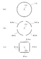
図1は本発明の半導体製造装置の一構成例を示す概略模式図であり、図中、1が、真空に排気しうる反応容器、2が排気口、3が基板ホルダー、4がヒーター、5が基板、5’が成膜面、6が石英管、7がマイクロ波導波管(プラズマ発生手段)、8、8’がガス導入管(ガス供給手段)、9aがガス導入管、9bがバルブ、9c、9dがガス管、10、10’がガス供給手段、11がガス導入管(ガス供給手段)、12が容量結合型高周波電極からなる円筒状電極(垂直吹き付けガス流活性化用プラズマ発生手段)、13がアース電極、13’がアース配線、14がRF(高周波)導入端子、20が垂直吹き付けガス流(のガス流れ方向中心軸)、21が放電方向、100が半導体装置を表す。
-Specific examples of semiconductor devices-
Next, specific examples of the semiconductor device of the present invention will be described with reference to the drawings.
FIG. 1 is a schematic diagram showing a configuration example of a semiconductor manufacturing apparatus according to the present invention. In the figure, 1 is a reaction vessel that can be evacuated, 2 is an exhaust port, 3 is a substrate holder, 4 is a heater, Is a substrate, 5 'is a film formation surface, 6 is a quartz tube, 7 is a microwave waveguide (plasma generating means), 8 and 8' are gas introduction pipes (gas supply means), 9a is a gas introduction pipe, and 9b is a valve. , 9c and 9d are gas pipes, 10 and 10 'are gas supply means, 11 is a gas introduction pipe (gas supply means), and 12 is a cylindrical electrode comprising a capacitively coupled high-frequency electrode (plasma generation for activating the vertical blowing gas flow) Means), 13 is a ground electrode, 13 'is ground wiring, 14 is an RF (high frequency) introduction terminal, 20 is a vertical blowing gas flow (center axis in the gas flow direction), 21 is a discharge direction, and 100 is a semiconductor device.
なお、以下の説明においては「垂直吹き付けガス流のガス流れ方向中心軸」という用語を用い、図中では矢印線で示しているが、現実にこのような中心軸が存在することを意味するものではない。これは、図面の説明を容易とする都合上、ガスが滞留することなく一方向へ最もスムーズに流れる領域の中心を、仮想的に示したものである。 In the following explanation, the term “center axis of the gas flow direction of the vertical blowing gas flow” is used and is indicated by an arrow line in the figure, but it means that such a center axis actually exists. is not. In order to facilitate the explanation of the drawings, this is a virtual representation of the center of the region where gas flows most smoothly in one direction without stagnation.
この半導体製造装置100は、略円筒状で、真空に排気しうる反応容器1を備えており、反応容器1内には、基板5を保持すると共に、基板5を加熱するためのヒーター4を内蔵した基板ホルダー3が設けられている。また、反応容器1には、この反応容器1内の基板5の成膜面5’側 (以下、「上側」、「上部」と称す)で、成膜面5’に対して略垂直な方向に石英管6が接続されており、成膜面5’と反対側(以下、「下側」、「下部」と称す)で、成膜面5’に対して略垂直な方向には排気口2が設けられており、石英管6の軸方向、反応容器1の軸方向、基板ホルダー5の中心部、排気口2の軸方向が概ね同一の直線上に位置するように配置されている。
This
石英管6の反応容器1が接続された側と反対側には反応容器1内へとガスを導入するガス導入管(ガス供給手段)11が接続されており、排気口2の反応容器1が接続された側と反対側には、反応容器1内のガスを排気する不図示の排気手段が接続されいる。また、石英管6の近傍には、石英管6内を流れるガスを活性化するために、石英管6と直交するようにマグネトロンを用いた不図示のマイクロ発振器に接続されたマイクロ波導波管7が設けられている。これにより、マイクロ波導波管7により石英管6内にはガス活性化領域が形成される。
A gas introduction pipe (gas supply means) 11 for introducing gas into the
従って、基板5の成膜面5’上に半導体薄膜を形成するためにガス導入管11から石英管6を経て反応容器1内へと活性化されたガスを導入すると共に、反応容器1内に導入されたガスを排気口2から排気する場合、マイクロ波導波管7により石英管6内で活性化されたガスが石英管6の出口(反応容器1との接続部)から、図中、符号20で示される矢印方向へと流れ、成膜面5’に対して略垂直に吹き付ける垂直吹き付けガス流20が形成される。
Accordingly, in order to form a semiconductor thin film on the
また、石英管6出口と成膜面5との間の反応容器1側壁には、上部から下部へと順に、垂直吹き付けガス流のガス流れ方向中心軸20に対して略対称に配置された、1対のガス供給手段10、10’、1対のガス導入管(ガス供給手段)8,8’、および、円筒状電極(垂直吹き付けガス流活性化用プラズマ発生手段)12が設けられている。
ここで、ガス供給手段10、10’は、反応容器1側壁を貫通するように配置されたガス導入管9aと、ガス導入管9aの反応容器1外壁側の端に接続されたバルブ9bと、バルブ9bに接続された2本のガス管9c、9dから構成され、不図示のガス供給源に接続されたガス管9c、9d内を流れるガスが、バルブ9b、ガス導入管9aを介して反応容器1内へと供給できるようになっている。なお、バルブ9bに接続されるガス管は2本以上であってもよい。
Further, on the side wall of the
Here, the gas supply means 10, 10 ′ include a gas introduction pipe 9 a arranged so as to penetrate the side wall of the
ガス導入管9aはノズル状で、先端が閉じた鋭い穴を有するものでも反対にラッパ状に開いたものでも良い。またノズル先端の位置は石英管6を成膜面5’側の軸方向に延長した同心円領域の内側でも外側でも良く、ノズル先端の位置を調整することにより、ノズル先端から放出されるガスが垂直吹き付けガス流20へと均一に合流できるように調整することができる。なお、図1に示す例では、ガス導入管9aは1対(2本)しか設けられていないが、2本以上であることが好ましく、多ければ多い方が良い。ガス導入管9aから反応容器1内に供給されるガスの種類やその混合割合、流量は、ガス種の切り替え・混合機能と流量調整機能とを備えたバルブ9bで調節することができる。
また、図1に示すガス導入管9aはノズル状であるが、このノズルは円形になっても良いし、メッシュ状であっても良い。また、成膜面5’に形成される半導体薄膜の膜厚のより一層の均一化のために、ノズルの先端にガスの拡散板を設けても良い。
The gas introduction pipe 9a is nozzle-shaped and may have a sharp hole with a closed tip or may be opened in a trumpet shape. Further, the position of the nozzle tip may be inside or outside the concentric region obtained by extending the
Moreover, although the gas introduction tube 9a shown in FIG. 1 is nozzle-shaped, this nozzle may be circular or mesh-shaped. Further, a gas diffusion plate may be provided at the tip of the nozzle in order to make the film thickness of the semiconductor thin film formed on the
一方、ガス供給手段10、10’の下流側に設けられるガス導入管8,8’に関しても、基本的に分岐構造を有していない点を除けば上述したガス供給手段10、10’と同様に、必要に応じて上述した種々の構成や配置を選択することができる。但し、ノズル先端の位置は、図1に示すように円筒状電極12の放電領域(ガス活性化領域)の外側に位置するように配置することが好ましい。
On the other hand, the
円筒状電極12は、その内周面(放電面)のいずれの位置からも、垂直吹き付けガス流のガス流れ方向中心軸20までの距離が略等距離の位置を保ち、且つ、垂直吹き付けガス流20の主流部から離れた位置に設置されている。このため、円筒状電極12からの放電により形成される放電領域(ガス活性化領域)内を通過する垂直吹き付けガス流20は、基板5の成膜面5’方向に対してほぼ一様に活性化される。このため、半導体製造装置100を用いて半導体薄膜を形成した場合、従来よりも成膜面5’に形成される半導体薄膜の面内組成をより均一にすることができる。
The
なお、円筒状電極12の外周面には、RF導入端子14が接続されており、このRF導入端子のもう一端は、反応容器1外部に設けられた不図示のRF発生装置と接続されている。さらに、円筒状電極12の外周側には円筒状のアース電極13が設けられており、アース電極13は、アース配線13により反応容器1の内壁に接地されている。
An
半導体製造装置100には、3つのガス供給手段8(8’)、11、10(10’)が設けられているが、半導体薄膜の形成に際しては、成膜する半導体の組成や成膜条件に応じて、1種以上の原料ガスを含むガスを1つ以上のガス供給手段を利用して反応容器1内へと供給することができる。
The
すなわち、原料ガスや補助ガスは、ガス供給手段11、ガス供給手段10,10’、ガス供給手段8,8’のいずれかから必要に応じて反応容器1内へと供給することができる。
但し、面内の組成および膜厚が均一な半導体薄膜を形成するためには、少なくとも1種の原料ガスが2つ以上の活性化領域を通過したのち成膜面5’に到達することが好ましく、この点で、少なくとも1種の原料ガスは最も上部に位置するガス供給手段11から供給されることが好ましい。
この場合、ガス供給手段11から成膜面5’へと垂直に吹き付ける安定したガスの流れ(垂直吹き付けガス流20)が形成されると共に、このガスの流れに沿って直列に配置された2つのプラズマ発生手段7,12によりガスが十分に活性化される。さらに、垂直吹き付けガス流20のガス流れ方向に対して横方向に配置されたガス供給手段10,10’や、ガス供給手段8,8’からもガスが供給される場合には、一旦活性化されたガスが、これら横方向から供給されるガスと合流してもガスの流れが乱れにくく、且つ、十分に混合される。
なお、原料ガスの活性化状態の制御や膜欠陥防止等のために利用される補助ガスは、円筒状電極12の上部近傍に位置するガス供給手段8,8’から供給されることが好ましい。
That is, the raw material gas and the auxiliary gas can be supplied into the
However, in order to form a semiconductor thin film having a uniform in-plane composition and film thickness, it is preferable that at least one source gas reaches the film-forming
In this case, a stable gas flow (vertical spraying gas flow 20) that blows vertically from the gas supply means 11 to the
The auxiliary gas used for controlling the activation state of the raw material gas and preventing film defects is preferably supplied from gas supply means 8 and 8 ′ located near the upper part of the
また、半導体製造装置100では、2種以上のガスを用いる場合においても均一に混合され、更に成膜面5’方向に対して均一に活性化された状態の垂直吹き付けガス流20が成膜面5’表面に吹き付けるため、成膜面5’面内方向の膜厚および組成が均一な半導体薄膜を得ることができる。
Further, in the
次に、この半導体製造装置100を用いて窒化物半導体膜としてGaInN膜を作製する場合について説明する。
まず、基板5を20〜1200℃に加熱し、例えば、原料としての窒素をガス導入管11から導入し、マイクロ波導波管7に2.45GHzのマイクロ波を供給し、石英管6内で放電させる。これにより窒素ガスは石英管6内で活性化された後、反応容器1内へと流入する。
この時、ガス管9aからキャリアガスと混合されたトリメチルガリウムガスを、ガス管9bからキャリアガスと混合されたトリメチルインジウムガスを導入し、バルブ9bで、所望の割合に混合すると共に、流量を調整し、ガス導入管9aより反応容器1内へと導入する。
Next, a case where a GaInN film is produced as a nitride semiconductor film using the
First, the
At this time, the trimethylgallium gas mixed with the carrier gas is introduced from the gas pipe 9a, and the trimethylindium gas mixed with the carrier gas is introduced from the gas pipe 9b, and mixed at a desired ratio by the valve 9b and the flow rate is adjusted. Then, the gas is introduced into the
このように、活性化された窒素ガスにIII族元素を含む原料ガスを導入することによって、活性化した窒素やラジカル、イオンによってIII族元素を含む原料ガスが分解されまたは反応し活性化種を生成する。
また、ガス導入管8から補助ガスとして水素ガスを導入する。なお、必要に応じて、水素ガスの代わりに、He、Arのような不活性気体を補助ガスとして導入してもよい。
In this way, by introducing the source gas containing the group III element into the activated nitrogen gas, the source gas containing the group III element is decomposed or reacted by the activated nitrogen, radicals, or ions, and the activated species is changed. Generate.
Further, hydrogen gas is introduced from the
このように3つのガス供給手段から供給された各々のガスは、合流して垂直吹き付けガス流20を形成し、成膜面5’に到達する前に円筒状電極によりさらに活性化される。こうして、成膜面5’に到達する直前の垂直吹き付けガス流20中には活性化されたIII族元素やV族元素が独立に制御された状態で存在し、また、活性化により生じた水素原子が、トリメチルガリウムやトリメチルインジウムのメチル基をメタン等の不活性分子にするため、炭素成分が含まれず膜欠陥が抑えられ、所望の組成に制御されると共に、面内の膜厚および組成が均一な窒化物半導体薄膜が成膜面5’上に形成される。
In this way, the gases supplied from the three gas supply means merge to form a vertical
次に、本発明の半導体製造装置の他の例を図面を用いて説明する。
図2は本発明の半導体製造装置の他の構成例を示す概略模式図であり、7’が高周波コイル(プラズマ発生手段)、200が半導体製造装置、他の符号は、図1に示すものと同様である。
図2に示す半導体製造装置は、図1に示す半導体製造装置100と基本的に同様の構成を有するものであるが、マイクロ波導波管7の代わりに石英管6の回りに巻きつけられた高周波コイル7’を備えた点が異なる。
この半導体製造装置200でも、基本的な構成は半導体製造装置100と同様であるため、面内の組成および膜厚が均一な半導体薄膜を形成することができる。
Next, another example of the semiconductor manufacturing apparatus of the present invention will be described with reference to the drawings.
FIG. 2 is a schematic diagram showing another configuration example of the semiconductor manufacturing apparatus according to the present invention, in which 7 ′ is a high-frequency coil (plasma generating means), 200 is a semiconductor manufacturing apparatus, and other symbols are those shown in FIG. It is the same.
The semiconductor manufacturing apparatus shown in FIG. 2 has basically the same configuration as that of the
Since the basic configuration of the
なお、図1,2に示すような本発明の半導体製造装置において、プラズマ発生手段による放電は直流放電でも交流放電でもよい。また、交流放電の場合、高周波放電の他低周波放電でもよい。さらに、高周波放電の場合、誘導型でも容量型でもよい。また、マイクロ発導波管のみならず、エレクトロンサイクロトロン共鳴方式やヘリコンプラズマ方式の導波管を使用してもよい。
また、本発明の半導体製造装置に用いられる複数のプラズマ発生手段の組み合わせは任意であり、図1,2に示すようなマイクロ波導波管と容量結合型高周波電極との組み合わせや、高周波コイルと容量結合型高周波電極との組み合わせに限られるものではない。
In the semiconductor manufacturing apparatus of the present invention as shown in FIGS. 1 and 2, the discharge by the plasma generating means may be direct current discharge or alternating current discharge. In the case of alternating current discharge, low frequency discharge may be used in addition to high frequency discharge. Furthermore, in the case of high frequency discharge, it may be inductive or capacitive. Further, not only a micro-waveguide but also an electron cyclotron resonance type or helicon plasma type waveguide may be used.
Moreover, the combination of the several plasma generation means used for the semiconductor manufacturing apparatus of this invention is arbitrary, the combination of a microwave waveguide and a capacitive coupling type | mold high frequency electrode as shown in FIG. It is not limited to the combination with the combined high-frequency electrode.
1つの空間において2種以上のプラズマ発生手段を用いる場合、同じ圧力で同時に放電が生起できるようにする必要があり、プラズマを発生する部分と、半導体を成膜する基板の近傍とに圧力差を設けてもよい。これらの圧力を同一とする場合、異なる種類のプラズマ発生手段、例えば、図1のようにマイクロ波導波管7と容量結合型高周波電極12とを用いると活性種の活性エネルギーを大きく変えることができ、膜質制御に有効である。
When two or more types of plasma generating means are used in one space, it is necessary to allow discharge to occur simultaneously at the same pressure, and a pressure difference is generated between a portion where plasma is generated and the vicinity of a substrate on which a semiconductor is formed. It may be provided. When these pressures are the same, the active energy of the active species can be greatly changed by using different types of plasma generating means, for example, the
また、基板ホルダー3は、上下方向に可動なものであってもよい。また、反応容器1内への基板5の出し入れが容易なように、反応容器1の内外を移動可能なものであってもよい。なお、本発明の半導体製造装置は、面内の膜厚および組成が均一な半導体薄膜が形成できるため、基本的には基板ホルダー3を成膜面5’方向に回転させる回転機構を設ける必要はないが、より一層の膜厚や組成の面内均一性が求められる場合には、必要に応じて回転機構を設けることもできる。
Further, the
さらに、半導体製造装置100,200ではガス導入管11は反応容器1の真上に配置されているが、ガス導入管11は石英管6の軸方向に対して斜めに傾斜していてもよい。
Furthermore, in the
なお、上述のような本発明の半導体製造装置を用いれば、基板上に半導体薄膜を形成することができるが、勿論、本発明の半導体製造装置は半導体膜膜以外のMOCVD法を利用して作製可能な薄膜の製造にも適用可能である。 If the semiconductor manufacturing apparatus of the present invention as described above is used, a semiconductor thin film can be formed on the substrate. Of course, the semiconductor manufacturing apparatus of the present invention is manufactured using MOCVD methods other than the semiconductor film. It can also be applied to the production of possible thin films.
−垂直吹き付けガス流活性化用プラズマ発生手段の他の具体例−
以上の図1,2に示した半導体装置の垂直吹き付けガス流活性化用プラズマ発生手段としては円筒状電極12が利用されていたが、このような板状電極を利用した他の垂直吹き付けガス流活性化用プラズマ発生手段の具体例を図1や2に示した半導体装置の構成を前提として図面を用いて説明する。
図3は、垂直吹き付けガス流のガス流れ方向と平行な面における板状電極(垂直吹き付けガス流活性化用プラズマ発生手段)の形状および配置の具体例を示す概略模式図であり、図中、30,31,32が板状電極を表し、他の符号は図1,2中に示すものと同様である。なお、図中、反応容器等やガス供給手段等の他の構成は省略している。
-Other specific examples of plasma generating means for vertical gas flow activation-
As the plasma generating means for activating the vertical blowing gas flow of the semiconductor device shown in FIGS. 1 and 2 above, the
FIG. 3 is a schematic diagram showing a specific example of the shape and arrangement of the plate-like electrodes (plasma generating means for activating the vertical blowing gas flow) on a plane parallel to the gas flow direction of the vertical blowing gas flow.
ここで、図3(a)は、図1や図2に示す板状電極(円筒状電極)12を示したものであり、放電面が真横を向き、垂直吹き付けガス流のガス流れ方向中心軸20と平行に配置されている。
これに対して、図3(b)に示す板状電極30のように放電面が若干下側を向き、垂直吹き付けガス流のガス流れ方向中心軸20に対してやや傾けた状態で配置したり、板状電極31のように放電面が若干上側を向き、垂直吹き付けガス流20のガス流れ方向に対してやや傾けた状態で配置したりすることもできる。
但し、垂直吹き付けガス流のガス流れ方向中心軸20に対して放電面が傾き過ぎると垂直吹き付けガス流の成膜面と平行な方向の活性化状態が不均一となり、成膜面内の組成が不均一となる場合があるため、放電面と垂直吹き付けガス流のガス流れ方向中心軸20との成す角度は、最大でも30度以下であることが好ましく、20度以下であることが好ましく、図3(a)に示すように0度であることが最も好ましい。
また、板状電極は、放電面が平坦なものに限定されるものではなく、例えば、図3(c)の板状電極32に示されるように、放電面が曲面であってもよい。
Here, FIG. 3A shows the plate electrode (cylindrical electrode) 12 shown in FIG. 1 and FIG. 2, and the discharge surface faces sideways and the central axis in the gas flow direction of the vertical blowing gas flow. 20 is arranged in parallel.
On the other hand, like the plate-shaped
However, if the discharge surface is too inclined with respect to the
Further, the plate-like electrode is not limited to the one having a flat discharge surface. For example, as shown in the plate-
一方、図3に対して、図4は、垂直吹き付けガス流のガス流れ方向と垂直に交わる面における板状電極(垂直吹き付けガス流活性化用プラズマ発生手段)の形状および配置の具体例を示す概略模式図であり、図中、33a〜33d、34a〜34dが板状電極を表し、他の符号は図1〜3中に示すものと同様である。なお、図中、反応容器等やガス供給手段等の他の構成は省略している。 On the other hand, FIG. 4 shows a specific example of the shape and arrangement of the plate-like electrode (plasma generating means for activating the vertical blowing gas flow) on the plane perpendicular to the gas flow direction of the vertical blowing gas flow. It is a schematic diagram, in which 33a-33d and 34a-34d represent a plate-like electrode, and other numerals are the same as those shown in FIGS. In the figure, other components such as a reaction vessel and a gas supply means are omitted.
ここで、図4(a)は、図1や図2に示す板状電極(円筒状電極)12を示したものであり、垂直吹き付けガス流のガス流れ方向中心軸20から等距離に位置するように1枚の連続した円筒状電極12が設けられている。
図4(a)に示す例は、垂直吹き付けガス流のガス流れ方向中心軸20から等距離に放電面が位置しており、理想的な電極形状ではある。しかし、半導体製造装置のメンテナンス性の向上や、装置構造の簡素化等、実用的な面も考慮した場合、図4(b)(c)に示すように、1枚の連続した円筒状電極を4つの部分に分割(電極33a、33b、33c、33d)したものであってもよく、放電面が平坦な電極(電極34a、34b、34c、34d)を4つ用いたものであってもよい。
この場合、4つの電極の各々に図1や図2に示されるようなアース配線が接続されたアース電極が電極の外周側に配置されると共に、RF(高周波)導入端子が接続される。
Here, FIG. 4A shows the plate-like electrode (cylindrical electrode) 12 shown in FIGS. 1 and 2, and is located at an equal distance from the
In the example shown in FIG. 4A, the discharge surface is located at an equal distance from the
In this case, each of the four electrodes is provided with an earth electrode connected to the earth wiring as shown in FIG. 1 or 2 on the outer peripheral side of the electrode, and an RF (high frequency) introduction terminal is connected.
(半導体製造システム)
また、本発明の半導体製造装置は、これを2つ以上含む半導体製造システムとしても利用できる。この場合、本発明の半導体製造システムは、基板が、大気雰囲気と遮断された状態でいずれか1つの半導体製造装置の反応容器から他の半導体製造装置の反応容器へと移動可能な基板搬送手段を備えていることが好ましい。
(Semiconductor manufacturing system)
The semiconductor manufacturing apparatus of the present invention can also be used as a semiconductor manufacturing system including two or more of them. In this case, the semiconductor manufacturing system of the present invention includes a substrate transfer means that can move from a reaction vessel of any one semiconductor manufacturing apparatus to a reaction container of another semiconductor manufacturing apparatus in a state where the substrate is cut off from the atmospheric air. It is preferable to provide.
このような半導体製造システムを使用することによって異なる活性化条件(例えば、放電電力、原料ガスの流量、ドーピング元素など)を用いて短時間で異なる組成の半導体薄膜(半導体層)を任意の膜厚で積層することが可能となる。
また、半導体層と半導体層との界面が大気に曝されて酸化されたりコンタミやパーティクル等により汚染されたりすること無く連続成膜・多層成膜ができるため、高性能で界面欠陥の少ない半導体素子を得ることができる。
By using such a semiconductor manufacturing system, a semiconductor thin film (semiconductor layer) having a different composition in a short time using different activation conditions (for example, discharge power, flow rate of source gas, doping element, etc.) Can be laminated.
In addition, because the interface between the semiconductor layer and the semiconductor layer is exposed to the atmosphere and is not oxidized or contaminated by contamination, particles, etc., it is possible to perform continuous film formation and multilayer film formation. Can be obtained.
一方、本発明の半導体製造システムは、本発明の半導体製造装置を利用しているため、大面積化しても各層の膜厚や組成が均一である。このため、大面積の基板上に半導体層が積層された1枚のウエハーを切り出して個々の半導体素子を作製しても、各々の素子間の性能ばらつきが小さく安定した品質の素子を得ることができる。さらに、従来、ウエハーの大面積化に伴い発生しやすい傾向にあった面内の膜厚や組成の不均一性に起因する歩留まり低下を抑制することができる。 On the other hand, since the semiconductor manufacturing system of the present invention uses the semiconductor manufacturing apparatus of the present invention, the film thickness and composition of each layer are uniform even when the area is increased. For this reason, even when a single wafer in which a semiconductor layer is stacked on a large-area substrate is cut out to produce individual semiconductor elements, it is possible to obtain a stable quality element with little variation in performance between the elements. it can. Furthermore, it is possible to suppress a decrease in yield due to in-plane film thickness and composition non-uniformity that has been apt to occur with an increase in wafer area.
なお、基板搬送手段としては、特に限定されないが、モータによりレール上を移動する等の可動式の基板ホルダーであることが好ましい。
また、1の半導体層が形成される反応容器(第1の反応容器)と他の半導体層が形成される反応容器(第2の反応容器)との間は、例えば、大気雰囲気と遮断された状態で基板の搬送が可能な連結室によって接続することができる。この場合、第1の反応容器中のガスあるいは第2の反応容器中のガスが、拡散や圧力差によって他方の反応容器中へと流れ込まないように、ガスの流れを遮断する開閉式のゲートが設けられていることが好ましい。このようなゲートを設けることにより個々の半導体層の膜質や組成の制御性をより向上させることができる。
The substrate transport means is not particularly limited, but is preferably a movable substrate holder that moves on a rail by a motor.
In addition, between the reaction vessel (first reaction vessel) in which one semiconductor layer is formed and the reaction vessel (second reaction vessel) in which another semiconductor layer is formed, for example, an air atmosphere is shut off. They can be connected by a connecting chamber capable of transporting the substrate in a state. In this case, an open / close gate that shuts off the gas flow is provided so that the gas in the first reaction vessel or the gas in the second reaction vessel does not flow into the other reaction vessel due to diffusion or pressure difference. It is preferable to be provided. By providing such a gate, the controllability of the film quality and composition of each semiconductor layer can be further improved.
これに対して、各々の半導体層の組成、膜質や成膜条件が類似している場合や、半導体製造システムの構成をより簡易化するために、本発明の半導体製造システムは、1つの反応容器を複数の半導体製造装置が共有する半導体製造システムであってもよい。
この場合、例えば、図1に示す半導体製造装置の基板ホルダー5よりも上部の構造部分(成膜システム)を、円形の反応容器の外周側に2つ以上接続した構成が挙げられる。この場合、反応容器の中心付近に基板ホルダーを設置し、各半導体層の形成に際しては、反応容器の外周側に接続された各々の成膜システム側から反応容器の中心へと流れる垂直吹き付けガス流に対して基板の成膜面が対向するように移動・回転させることで、各々の半導体層を基板上に積層することができる。
On the other hand, in the case where the composition, film quality, and film forming conditions of each semiconductor layer are similar, or in order to further simplify the configuration of the semiconductor manufacturing system, the semiconductor manufacturing system of the present invention includes one reaction vessel. May be a semiconductor manufacturing system shared by a plurality of semiconductor manufacturing apparatuses.
In this case, for example, a configuration in which two or more structural parts (film formation system) above the
1 真空に排気しうる反応容器
2 排気口
3 基板ホルダー
4 ヒーター
5 基板
5’ 成膜面
6 石英管
7 マイクロ波導波管(プラズマ発生手段)
7’ 高周波コイル(プラズマ発生手段)
8、8’ ガス導入管(ガス供給手段)
9a ガス導入管
9b バルブ
9c、9d ガス管
10、10’ ガス供給手段
11 ガス導入管(ガス供給手段)
12 円筒状(板状)電極(垂直吹き付けガス流活性化用プラズマ発生手段)
13 アース電極
13’ アース配線
14 RF(高周波)導入端子
20 垂直吹き付けガス流(のガス流れ方向中心軸)
21 放電方向
30,31,32、33a〜33d、34a〜34d 板状電極
100、200 半導体装置
DESCRIPTION OF
7 'High frequency coil (plasma generating means)
8, 8 'Gas introduction pipe (gas supply means)
9a Gas introduction pipe 9b Valve 9c,
12 Cylindrical (plate) electrode (plasma generating means for vertical gas flow activation)
13 Ground electrode 13 '
21
Claims (5)
少なくとも1つ以上のプラズマ発生手段により活性化されたガスが、前記成膜面に対して略垂直に吹き付ける垂直吹き付けガス流が形成される半導体製造装置において、
前記複数のプラズマ発生手段として、V族元素を含む第1の原料ガスを活性化する第1のプラズマ発生手段と、
該第1のプラズマ発生手段および前記複数のガス供給手段よりも前記垂直吹き付けガス流のガス流れ方向下流側に設けられ前記垂直吹き付けガス流のガス流れ方向中心に向かってプラズマ放電を行い、前記ガスを活性化する垂直吹き付けガス流活性化用プラズマ発生手段とを設け、
前記複数のガス供給手段として、前記第1の原料ガスを供給し前記反応容器内に前記垂直吹き付けガス流を形成する第1のガス供給手段と、
該第1のガス供給手段よりも前記垂直吹き付けガス流のガス流れ方向下流側であり且つ前記垂直吹き付けガス流活性化用プラズマ発生手段よりも前記垂直吹き付けガス流のガス流れ方向上流側に設けられ前記第1の原料ガスとは異なるIII族元素を含む第2の原料ガスを前記垂直吹き付けガス流に合流するように供給する第2のガス供給手段と、
前記第1のガス供給手段よりも前記垂直吹き付けガス流のガス流れ方向下流側であり且つ前記垂直吹き付けガス流活性化用プラズマ発生手段よりも前記垂直吹き付けガス流のガス流れ方向上流側に設けられ前記垂直吹き付けガス流に合流するように補助ガスを供給する第3のガス供給手段とを設けたことを特徴とする半導体製造装置。 A reaction vessel, a substrate holder for holding a substrate, a plurality of gas supply means for supplying a raw material gas and the auxiliary gas, in one surface of the substrate from the gas supply means is in said reaction vessel A plurality of plasma generating means arranged to activate the gas flowing in the direction of the film formation surface,
In a semiconductor manufacturing apparatus in which a gas flow activated by at least one or more plasma generating means is blown substantially perpendicularly to the film-forming surface is formed.
A first plasma generating means for activating a first source gas containing a group V element as the plurality of plasma generating means;
The plasma is discharged toward the center in the gas flow direction of the vertical blowing gas flow provided downstream of the first plasma generating means and the plurality of gas supply means in the gas flow direction of the vertical blowing gas flow, and the gas And a plasma generating means for activating the vertical blowing gas flow for activating
As the plurality of gas supply means, a first gas supply means for supplying the first source gas and forming the vertical blowing gas flow in the reaction vessel;
Provided downstream of the first gas supply means in the gas flow direction of the vertical blowing gas flow and upstream of the vertical blowing gas flow activation plasma generation means in the gas flow direction of the vertical blowing gas flow. A second gas supply means for supplying a second source gas containing a group III element different from the first source gas so as to merge with the vertical blowing gas stream;
Provided downstream of the first gas supply means in the gas flow direction of the vertical blowing gas flow and upstream of the vertical blowing gas flow activation plasma generation means in the gas flow direction of the vertical blowing gas flow. 3. A semiconductor manufacturing apparatus, comprising: a third gas supply means for supplying an auxiliary gas so as to merge with the vertical blowing gas flow.
少なくとも1つ以上のプラズマ発生手段により活性化されたガスが、前記成膜面に対して略垂直に吹き付ける垂直吹き付けガス流が形成され、
前記複数のプラズマ発生手段として、V族元素を含む第1の原料ガスを活性化する第1のプラズマ発生手段と、
該第1のプラズマ発生手段および前記複数のガス供給手段よりも前記垂直吹き付けガス流のガス流れ方向下流側に設けられ前記垂直吹き付けガス流のガス流れ方向中心に向かってプラズマ放電を行い、前記ガスを活性化する垂直吹き付けガス流活性化用プラズマ発生手段とを設け、
前記複数のガス供給手段として、前記第1の原料ガスを供給し前記反応容器内に前記垂直吹き付けガス流を形成する第1のガス供給手段と、
該第1のガス供給手段よりも前記垂直吹き付けガス流のガス流れ方向下流側であり且つ前記垂直吹き付けガス流活性化用プラズマ発生手段よりも前記垂直吹き付けガス流のガス流れ方向上流側に設けられ前記第1の原料ガスとは異なるIII族元素を含む第2の原料ガスを前記垂直吹き付けガス流に合流するように供給する第2のガス供給手段と、
前記第1のガス供給手段よりも前記垂直吹き付けガス流のガス流れ方向下流側であり且つ前記垂直吹き付けガス流活性化用プラズマ発生手段よりも前記垂直吹き付けガス流のガス流れ方向上流側に設けられ前記垂直吹き付けガス流に合流するように補助ガスを供給する第3のガス供給手段とを設けた半導体製造装置を2つ以上含む半導体製造システムであって、
前記基板が、大気雰囲気と遮断された状態でいずれか1つの半導体製造装置の反応容器から他の半導体製造装置の反応容器へと移動可能な基板搬送手段を備えたことを特徴とする半導体製造システム。 A reaction vessel, a substrate holder for holding a substrate, a plurality of gas supply means for supplying a raw material gas and the auxiliary gas, in one surface of the substrate from the gas supply means is in said reaction vessel A plurality of plasma generating means arranged to activate the gas flowing in the direction of the film formation surface,
A gas stream activated by at least one or more plasma generating means is formed so as to blow substantially perpendicularly to the film-forming surface;
A first plasma generating means for activating a first source gas containing a group V element as the plurality of plasma generating means;
The plasma is discharged toward the center in the gas flow direction of the vertical blowing gas flow provided downstream of the first plasma generating means and the plurality of gas supply means in the gas flow direction of the vertical blowing gas flow, and the gas And a plasma generating means for activating the vertical blowing gas flow for activating
As the plurality of gas supply means, a first gas supply means for supplying the first source gas and forming the vertical blowing gas flow in the reaction vessel;
Provided downstream of the first gas supply means in the gas flow direction of the vertical blowing gas flow and upstream of the vertical blowing gas flow activation plasma generation means in the gas flow direction of the vertical blowing gas flow. A second gas supply means for supplying a second source gas containing a group III element different from the first source gas so as to merge with the vertical blowing gas stream;
Provided downstream of the first gas supply means in the gas flow direction of the vertical blowing gas flow and upstream of the vertical blowing gas flow activation plasma generation means in the gas flow direction of the vertical blowing gas flow. A semiconductor manufacturing system including two or more semiconductor manufacturing apparatuses provided with a third gas supply means for supplying an auxiliary gas so as to join the vertical blowing gas flow,
A semiconductor manufacturing system comprising a substrate transfer means that is movable from a reaction vessel of any one semiconductor manufacturing apparatus to a reaction container of another semiconductor manufacturing apparatus in a state where the substrate is cut off from the atmospheric air .
Priority Applications (2)
| Application Number | Priority Date | Filing Date | Title |
|---|---|---|---|
| JP2004163892A JP5011631B2 (en) | 2004-06-01 | 2004-06-01 | Semiconductor manufacturing apparatus and semiconductor manufacturing system |
| US11/006,578 US20050263071A1 (en) | 2004-06-01 | 2004-12-08 | Apparatus and system for manufacturing a semiconductor |
Applications Claiming Priority (1)
| Application Number | Priority Date | Filing Date | Title |
|---|---|---|---|
| JP2004163892A JP5011631B2 (en) | 2004-06-01 | 2004-06-01 | Semiconductor manufacturing apparatus and semiconductor manufacturing system |
Publications (3)
| Publication Number | Publication Date |
|---|---|
| JP2005347426A JP2005347426A (en) | 2005-12-15 |
| JP2005347426A5 JP2005347426A5 (en) | 2007-07-12 |
| JP5011631B2 true JP5011631B2 (en) | 2012-08-29 |
Family
ID=35423809
Family Applications (1)
| Application Number | Title | Priority Date | Filing Date |
|---|---|---|---|
| JP2004163892A Active JP5011631B2 (en) | 2004-06-01 | 2004-06-01 | Semiconductor manufacturing apparatus and semiconductor manufacturing system |
Country Status (2)
| Country | Link |
|---|---|
| US (1) | US20050263071A1 (en) |
| JP (1) | JP5011631B2 (en) |
Families Citing this family (3)
| Publication number | Priority date | Publication date | Assignee | Title |
|---|---|---|---|---|
| JP5044860B2 (en) * | 2007-03-14 | 2012-10-10 | 積水化学工業株式会社 | Method for forming group III nitride such as gallium nitride |
| US20090258162A1 (en) * | 2008-04-12 | 2009-10-15 | Applied Materials, Inc. | Plasma processing apparatus and method |
| US9277637B2 (en) * | 2010-11-17 | 2016-03-01 | Tokyo Electron Limited | Apparatus for plasma treatment and method for plasma treatment |
Family Cites Families (11)
| Publication number | Priority date | Publication date | Assignee | Title |
|---|---|---|---|---|
| DE3378508D1 (en) * | 1982-09-10 | 1988-12-22 | Nippon Telegraph & Telephone | Plasma deposition method and apparatus |
| JP2598336B2 (en) * | 1990-09-21 | 1997-04-09 | 株式会社日立製作所 | Plasma processing equipment |
| JPH07161647A (en) * | 1993-12-07 | 1995-06-23 | Sony Corp | Surface treater |
| JP3151596B2 (en) * | 1995-07-20 | 2001-04-03 | 東京エレクトロン株式会社 | Plasma processing method and apparatus |
| US6152070A (en) * | 1996-11-18 | 2000-11-28 | Applied Materials, Inc. | Tandem process chamber |
| US6194038B1 (en) * | 1998-03-20 | 2001-02-27 | Applied Materials, Inc. | Method for deposition of a conformal layer on a substrate |
| JP2976965B2 (en) * | 1998-04-02 | 1999-11-10 | 日新電機株式会社 | Film forming method and film forming apparatus |
| JP2000188257A (en) * | 1998-12-22 | 2000-07-04 | Sharp Corp | Manufacture of crystalline silicon-based semiconductor thin film |
| JP3757698B2 (en) * | 1999-09-07 | 2006-03-22 | 富士ゼロックス株式会社 | Semiconductor manufacturing apparatus and semiconductor manufacturing system |
| JP2001177099A (en) * | 1999-12-14 | 2001-06-29 | Furontekku:Kk | Manufacturing method of thin-film transistor, active matrix substrate, and thin-film deposition device |
| US7115516B2 (en) * | 2001-10-09 | 2006-10-03 | Applied Materials, Inc. | Method of depositing a material layer |
-
2004
- 2004-06-01 JP JP2004163892A patent/JP5011631B2/en active Active
- 2004-12-08 US US11/006,578 patent/US20050263071A1/en not_active Abandoned
Also Published As
| Publication number | Publication date |
|---|---|
| US20050263071A1 (en) | 2005-12-01 |
| JP2005347426A (en) | 2005-12-15 |
Similar Documents
| Publication | Publication Date | Title |
|---|---|---|
| KR950012910B1 (en) | Vapor phase growth apparatus | |
| TWI743135B (en) | Showerhead curtain gas method and system for film profile modulation | |
| JP4931082B2 (en) | Gas head and thin film manufacturing apparatus | |
| JP6157942B2 (en) | Vapor growth apparatus and vapor growth method | |
| JP6386901B2 (en) | Vapor growth apparatus and vapor growth method | |
| KR20150006354A (en) | Vapor growth device and vapor growth method | |
| US6004885A (en) | Thin film formation on semiconductor wafer | |
| JP5011631B2 (en) | Semiconductor manufacturing apparatus and semiconductor manufacturing system | |
| WO2012120991A1 (en) | Substrate processing apparatus and method for manufacturing substrate | |
| CN111188027B (en) | Chemical vapor deposition equipment and film forming method | |
| JP2009099972A (en) | Vapor deposition device, and manufacturing method of semiconductor device | |
| JP3757698B2 (en) | Semiconductor manufacturing apparatus and semiconductor manufacturing system | |
| JP2007109685A (en) | Apparatus and method for manufacturing compound semiconductor | |
| US20200149164A1 (en) | Thermal metal chemical vapor deposition apparatus and process | |
| US20190271083A1 (en) | Film formation apparatus | |
| TW200538578A (en) | Microcontamination abatement in semiconductor processing | |
| WO2023008295A1 (en) | Method for producing group iii-nitride semiconductor | |
| KR102208609B1 (en) | Shower head for chemical vapor deposition and depositing apparatus using the same | |
| JP2003100642A (en) | Vapor phase thin film epitaxial growth system and vapor phase thin film epitaxial growth method | |
| TW202208679A (en) | Apparatus for processing substrate | |
| JPH03255619A (en) | Vertical type cvd device | |
| KR101087974B1 (en) | Chemical vapor deposition appratus | |
| JP2012190902A (en) | Vapor phase epitaxial growth device, and vapor phase epitaxial growth method | |
| JPH11186171A (en) | Semiconductor manufacturing device | |
| KR20090070035A (en) | Chemical vapor deposition device |
Legal Events
| Date | Code | Title | Description |
|---|---|---|---|
| A621 | Written request for application examination |
Free format text: JAPANESE INTERMEDIATE CODE: A621 Effective date: 20070517 |
|
| A521 | Written amendment |
Free format text: JAPANESE INTERMEDIATE CODE: A523 Effective date: 20070530 |
|
| A977 | Report on retrieval |
Free format text: JAPANESE INTERMEDIATE CODE: A971007 Effective date: 20090807 |
|
| A131 | Notification of reasons for refusal |
Free format text: JAPANESE INTERMEDIATE CODE: A131 Effective date: 20100309 |
|
| A521 | Written amendment |
Free format text: JAPANESE INTERMEDIATE CODE: A523 Effective date: 20100506 |
|
| A131 | Notification of reasons for refusal |
Free format text: JAPANESE INTERMEDIATE CODE: A131 Effective date: 20110405 |
|
| A521 | Written amendment |
Free format text: JAPANESE INTERMEDIATE CODE: A523 Effective date: 20110606 |
|
| A131 | Notification of reasons for refusal |
Free format text: JAPANESE INTERMEDIATE CODE: A131 Effective date: 20120214 |
|
| A521 | Written amendment |
Free format text: JAPANESE INTERMEDIATE CODE: A523 Effective date: 20120413 |
|
| TRDD | Decision of grant or rejection written | ||
| A01 | Written decision to grant a patent or to grant a registration (utility model) |
Free format text: JAPANESE INTERMEDIATE CODE: A01 Effective date: 20120508 |
|
| A01 | Written decision to grant a patent or to grant a registration (utility model) |
Free format text: JAPANESE INTERMEDIATE CODE: A01 |
|
| A61 | First payment of annual fees (during grant procedure) |
Free format text: JAPANESE INTERMEDIATE CODE: A61 Effective date: 20120521 |
|
| FPAY | Renewal fee payment (event date is renewal date of database) |
Free format text: PAYMENT UNTIL: 20150615 Year of fee payment: 3 |
|
| R150 | Certificate of patent or registration of utility model |
Free format text: JAPANESE INTERMEDIATE CODE: R150 Ref document number: 5011631 Country of ref document: JP Free format text: JAPANESE INTERMEDIATE CODE: R150 |
|
| S533 | Written request for registration of change of name |
Free format text: JAPANESE INTERMEDIATE CODE: R313533 |
|
| R350 | Written notification of registration of transfer |
Free format text: JAPANESE INTERMEDIATE CODE: R350 |