JP5010239B2 - Compensated amplifier - Google Patents
Compensated amplifier Download PDFInfo
- Publication number
- JP5010239B2 JP5010239B2 JP2006299309A JP2006299309A JP5010239B2 JP 5010239 B2 JP5010239 B2 JP 5010239B2 JP 2006299309 A JP2006299309 A JP 2006299309A JP 2006299309 A JP2006299309 A JP 2006299309A JP 5010239 B2 JP5010239 B2 JP 5010239B2
- Authority
- JP
- Japan
- Prior art keywords
- amplifier
- input
- output
- capacitor
- amplifiers
- Prior art date
- Legal status (The legal status is an assumption and is not a legal conclusion. Google has not performed a legal analysis and makes no representation as to the accuracy of the status listed.)
- Active
Links
Images


Classifications
-
- H—ELECTRICITY
- H03—ELECTRONIC CIRCUITRY
- H03F—AMPLIFIERS
- H03F1/00—Details of amplifiers with only discharge tubes, only semiconductor devices or only unspecified devices as amplifying elements
- H03F1/42—Modifications of amplifiers to extend the bandwidth
-
- H—ELECTRICITY
- H03—ELECTRONIC CIRCUITRY
- H03F—AMPLIFIERS
- H03F1/00—Details of amplifiers with only discharge tubes, only semiconductor devices or only unspecified devices as amplifying elements
- H03F1/26—Modifications of amplifiers to reduce influence of noise generated by amplifying elements
-
- H—ELECTRICITY
- H03—ELECTRONIC CIRCUITRY
- H03F—AMPLIFIERS
- H03F3/00—Amplifiers with only discharge tubes or only semiconductor devices as amplifying elements
- H03F3/005—Amplifiers with only discharge tubes or only semiconductor devices as amplifying elements using switched capacitors, e.g. dynamic amplifiers; using switched capacitors as resistors in differential amplifiers
-
- H—ELECTRICITY
- H03—ELECTRONIC CIRCUITRY
- H03F—AMPLIFIERS
- H03F2200/00—Indexing scheme relating to amplifiers
- H03F2200/18—Indexing scheme relating to amplifiers the bias of the gate of a FET being controlled by a control signal
-
- H—ELECTRICITY
- H03—ELECTRONIC CIRCUITRY
- H03F—AMPLIFIERS
- H03F2200/00—Indexing scheme relating to amplifiers
- H03F2200/36—Indexing scheme relating to amplifiers the amplifier comprising means for increasing the bandwidth
Landscapes
- Engineering & Computer Science (AREA)
- Power Engineering (AREA)
- Amplifiers (AREA)
Description
[0001]本願は、2006年7月31日に出願された米国仮出願第60/820,878号及び2006年5月10日に出願された米国仮出願第60/799,282号の利益を主張するものであり、2005年11月2日に出願された米国特許出願第11/264,921号の一部継続出願である。上記出願の開示内容は、その全体を参照することによって本明細書に組み込む。 [0001] This application claims the benefit of US Provisional Application No. 60 / 820,878 filed July 31, 2006 and US Provisional Application No. 60 / 799,282 filed May 10, 2006. This is a continuation-in-part of U.S. Patent Application No. 11 / 264,921, filed on November 2, 2005. The disclosure of the above application is incorporated herein by reference in its entirety.
[0002]本発明は、増幅器に関するものであり、特に、補償付き増幅器に関するものである。 [0002] The present invention relates to amplifiers, and more particularly to compensated amplifiers.
[0003]増幅器は、1段以上のステージを含むことがある。各ステージは利得を提供する増幅器を含むことがある。周波数が増加するにつれて、増幅器によって提供される利得は低下し、このことが増幅器の帯域幅を制限する。電子計算デバイスの動作周波数が増加するにつれて、高帯域幅、高利得、そして低雑音を有する増幅器が徐々に重要になってきている。 [0003] An amplifier may include one or more stages. Each stage may include an amplifier that provides gain. As the frequency increases, the gain provided by the amplifier decreases, which limits the bandwidth of the amplifier. As the operating frequency of electronic computing devices increases, amplifiers with high bandwidth, high gain, and low noise are becoming increasingly important.
[0004]ミラー補償は、利得ステージの実効入力キャパシタンスを増加させることによって、利得ステージの主要極をより低い周波数へ移動させる従来型の周波数補償技術である。ミラー補償回路は、ミラー効果を利用するミラーキャパシタンスを含む。ミラーキャパシタンスがフィードバック構成に接続される場合に、キャパシタンスは増幅器の入力にでは非常に大きく見える。主要極は、この方法を用いてより低い周波数へ移されるが、システムの利得及び帯域幅は依然として多少制限されている。 [0004] Miller compensation is a conventional frequency compensation technique that moves the main pole of the gain stage to a lower frequency by increasing the effective input capacitance of the gain stage. The mirror compensation circuit includes a mirror capacitance that utilizes the mirror effect. When the mirror capacitance is connected in a feedback configuration, the capacitance appears very large at the amplifier input. The main pole is moved to lower frequencies using this method, but the gain and bandwidth of the system is still somewhat limited.
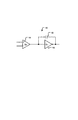
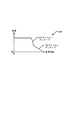
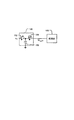
[0005]ここで、図1及び2を参照する。これらの図は、ミラー補償付きの増幅器回路10を示しており、当該回路10は、第1の増幅器14及び第2の増幅器16を含んでいる。第1の増幅器14の出力は、第2の増幅器16の入力に接続している。ミラーキャパシタンス18の第1の端部は、第2の増幅器16の入力に接続しており、ミラーキャパシタンス18の第2の端部は、第2の増幅器16の出力に接続している。
[0005] Reference is now made to FIGS. These figures show an
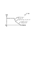
[0006]増幅器回路10の入力電圧は、第1の増幅器14の入力に印加される。増幅器回路10の出力電圧は、第2の増幅器16の出力から参照される。ミラー補償の結果、第2の増幅器16のトランスコンダクタンスgmが増大され、このことが増幅器回路10の帯域幅を増大する。図2において見ることができるように、ミラー補償付きの増幅器の利得は20dB/decadeの傾きを有する。
[0006] The input voltage of the
[0007]増幅器はスイッチドキャパシタ入力信号と共に使用されることもある。スイッチドキャパシタ入力信号は、アナログ・デジタル変換器(ADC)、デジタル・アナログ変換器(DAC)、フィルタ、及び/又は、その他の回路で生成される。図1に示すような従来型の増幅器は、特にスイッチドキャパシタ入力信号に対して、許容可能な雑音レベルで十分な利得及び帯域幅を提供することが難しいときがある。 [0007] An amplifier may be used with a switched capacitor input signal. The switched capacitor input signal is generated by an analog to digital converter (ADC), a digital to analog converter (DAC), a filter, and / or other circuitry. A conventional amplifier as shown in FIG. 1 may be difficult to provide sufficient gain and bandwidth at an acceptable noise level, especially for switched capacitor input signals.
[0008]増幅器システムは、第1の増幅器、第2の増幅器、第1のキャパシタ、及び第1のトランジスタを備える。第1の増幅器は、入力及び出力を有する。第2の増幅器は、第1の増幅器の出力に接続する入力を有する。第1のキャパシタは第1の増幅器の入力に接続する一端を有する。第1のトランジスタは、制御端子、第1の増幅器の出力に接続する第1の端子、及び第1のキャパシタの他端に接続する第2の端子を有する。 [0008] The amplifier system comprises a first amplifier, a second amplifier, a first capacitor, and a first transistor. The first amplifier has an input and an output. The second amplifier has an input connected to the output of the first amplifier. The first capacitor has one end connected to the input of the first amplifier. The first transistor has a control terminal, a first terminal connected to the output of the first amplifier, and a second terminal connected to the other end of the first capacitor.
[0009]別の特徴において、増幅器システムは、第1のトランジスタの第2の端子に接続する第1の電流源を更に備える。 [0009] In another feature, the amplifier system further comprises a first current source connected to the second terminal of the first transistor.
[0010]別の特徴において、増幅器システムは、第1のトランジスタの第1の端子に接続する第2の電流源を更に備える。 [0010] In another feature, the amplifier system further comprises a second current source connected to the first terminal of the first transistor.
[0011]別の特徴において、増幅器システムは、第1のトランジスタの第2の端子に接続する第1の電流源と、第1のトランジスタの第1の端子に接続する第2の電流源とを更に備える。 [0011] In another feature, an amplifier system includes: a first current source connected to the second terminal of the first transistor; and a second current source connected to the first terminal of the first transistor. In addition.
[0012]別の特徴において、第1及び第2の増幅器は、演算トランスコンダクタンス増幅器を含む。 [0012] In another feature, the first and second amplifiers include operational transconductance amplifiers.
[0013]別の特徴において、第1及び第2の増幅器は、演算増幅器を含む。 [0013] In another feature, the first and second amplifiers include operational amplifiers.
[0014]更に別の特徴において、増幅器システムは、第1の増幅器、第2の増幅器、第1のキャパシタ、第2のキャパシタ、及び第1のトランジスタを備える。第1の増幅器は、入力及び出力を有する。第2の増幅器は、第1の増幅器の出力に接続する入力を有する。第1のキャパシタは、第1の増幅器の入力に接続する一端を有する。第2のキャパシタは、第2の増幅器の入力に接続する一端を有する。第1のトランジスタは、制御端子、第2のキャパシタの他端に接続する第1の端子、及び第1のキャパシタの他端に接続する第2の端子を有する。 [0014] In yet another feature, the amplifier system comprises a first amplifier, a second amplifier, a first capacitor, a second capacitor, and a first transistor. The first amplifier has an input and an output. The second amplifier has an input connected to the output of the first amplifier. The first capacitor has one end connected to the input of the first amplifier. The second capacitor has one end connected to the input of the second amplifier. The first transistor has a control terminal, a first terminal connected to the other end of the second capacitor, and a second terminal connected to the other end of the first capacitor.
[0015]別の特徴において、増幅器システムは、第1のトランジスタの第2の端子に接続する第1の電流源を更に備える。 [0015] In another feature, the amplifier system further comprises a first current source connected to the second terminal of the first transistor.
[0016]別の特徴において、増幅器システムは、第2の増幅器の入力に接続する第2の電流源を更に備える。 [0016] In another feature, the amplifier system further comprises a second current source connected to the input of the second amplifier.
[0017]別の特徴において、増幅器システムは、第1のトランジスタの第2の端子に接続する第1の電流源と、第2の増幅器の入力に接続する第2の電流源と、を更に備える。 [0017] In another feature, the amplifier system further comprises a first current source connected to the second terminal of the first transistor and a second current source connected to the input of the second amplifier. .
[0018]別の特徴において、第1及び第2の増幅器は演算トランスコンダクタンス増幅器を含む。 [0018] In another feature, the first and second amplifiers include operational transconductance amplifiers.
[0019]別の特徴において、第1及び第2の増幅器は演算増幅器を含む。 [0019] In another feature, the first and second amplifiers include operational amplifiers.
[0020]更に別の特徴において、増幅器システムは、入力及び出力を有する第1の増幅手段と、第1の増幅手段の出力に接続する入力を有する第2の増幅手段と、第1の増幅手段の入力に接続する一端を有する第1のキャパシタンス手段と、制御端子、第1の増幅手段の出力に接続する第1の端子、及び第1のキャパシタンス手段の他端に接続する第2の端子を有する第1のトランジスタと、を備える。 [0020] In yet another feature, the amplifier system includes a first amplifying means having an input and an output, a second amplifying means having an input connected to the output of the first amplifying means, and a first amplifying means. A first capacitance means having one end connected to the input, a control terminal, a first terminal connected to the output of the first amplifying means, and a second terminal connected to the other end of the first capacitance means. And a first transistor.
[0021]別の特徴において、増幅器システムは、第1のトランジスタの第2の端子に接続する第1の電流源手段を更に備える。 [0021] In another feature, the amplifier system further comprises first current source means connected to the second terminal of the first transistor.
[0022]別の特徴において、増幅器システムは、第1のトランジスタの第1の端子に接続する第2の電流源手段を更に備える。 [0022] In another feature, the amplifier system further comprises second current source means connected to the first terminal of the first transistor.
[0023]別の特徴において、増幅器システムは、第1のトランジスタの第2の端子に接続する第1の電流源手段と、第1のトランジスタの第1の端子に接続する第2の電流源手段とをさらに備える。 [0023] In another feature, the amplifier system includes a first current source means connected to the second terminal of the first transistor and a second current source means connected to the first terminal of the first transistor. And further comprising.
[0024]別の特徴において、第1及び第2の増幅手段は、演算トランスコンダクタンス増幅器を含む。 [0024] In another feature, the first and second amplifying means include operational transconductance amplifiers.
[0025]別の特徴において、第1及び第2の増幅手段は、演算増幅器を含む。 [0025] In another feature, the first and second amplification means include operational amplifiers.
[0026]更に別の特徴において、増幅器システムは、入力及び出力を有する増幅用の第1の増幅手段と、第1の増幅手段の出力に接続する入力を有する増幅用の第2の増幅手段と、第1の増幅手段の入力に接続する一端を有するキャパシタを提供する第1のキャパシタンス手段と、第2の増幅手段の入力に接続する一端を有するキャパシタを提供する第2のキャパシタンス手段と、制御端子、第2のキャパシタンス手段の他端に接続する第1の端子、及び第1のキャパシタンス手段の他端に接続する第2の端子を有する第1のトランジスタと、を備える。 [0026] In yet another feature, an amplifier system includes a first amplifying means for amplification having an input and an output, and a second amplifying means for amplification having an input connected to the output of the first amplifying means. A first capacitance means for providing a capacitor having one end connected to the input of the first amplifying means; a second capacitance means for providing a capacitor having one end connected to the input of the second amplifying means; A first transistor having a terminal, a first terminal connected to the other end of the second capacitance means, and a second terminal connected to the other end of the first capacitance means.
[0027]別の特徴において、増幅器システムは、電流を供給し第1のトランジスタの第2の端子に接続する第1の電流源手段を更に備える。 [0027] In another feature, the amplifier system further comprises first current source means for supplying current and connecting to the second terminal of the first transistor.
[0028]別の特徴において、増幅器システムは、電流を供給し第2の増幅手段の入力に接続する第2の電流源手段を更に備える。 [0028] In another feature, the amplifier system further comprises second current source means for supplying current and connecting to an input of the second amplifying means.
[0029]別の特徴において、増幅器システムは、電流を供給し第1のトランジスタの第2の端子に接続する第1の電流源手段と、電流を供給し第2の増幅器の入力に接続する第2の電流源手段と、を更に備える。 [0029] In another feature, the amplifier system includes a first current source means for supplying current and connecting to the second terminal of the first transistor; and a first current source for supplying current and connecting to the input of the second amplifier. Two current source means.
[0030]別の特徴において、第1及び第2の増幅手段は、演算トランスコンダクタンス増幅器を含む。 [0030] In another feature, the first and second amplification means include operational transconductance amplifiers.
[0031]別の特徴において、第1及び第2の増幅手段は、演算増幅器を含む。 [0031] In another feature, the first and second amplification means include operational amplifiers.
[0032]本発明の更なる適用範囲は、以下に記載する詳細な説明から明白になる。詳細な説明及び具体的な実施例は、発明の好ましい実施形態を示すが、例示の目的だけを意図するものであり、発明の範囲を制限することを意図するものではないことを理解すべきである。 [0032] Further scope of applicability of the present invention will become apparent from the detailed description provided hereinafter. It should be understood that the detailed description and specific examples, while indicating the preferred embodiment of the invention, are intended for purposes of illustration only and are not intended to limit the scope of the invention. is there.
[0033]本発明は、詳細な説明及び添付図面からより完全に理解されよう。 [0033] The present invention will become more fully understood from the detailed description and the accompanying drawings, wherein:
[0059]以下の(複数の)好ましい実施形態の説明は、本質的に単なる例示であり、決して発明、発明の応用、又は、発明の使用を制限することを意図するものではない。本明細書で使用されるように、モジュール、回路、及び/又は、装置という用語は、特定用途向け集積回路(ASIC)、電子回路、一つ以上のソフトウェア又はファームウェアプログラムを実行するプロセッサ(共有、専用、又は、グループ)及びメモリ、組み合わせ論理回路、並びに/若しくは、上記の機能を提供するその他の適当なコンポーネントを指す。本明細書で使用されるように、A、B、及びCのうちの少なくとも一つという語句は、非排他的論理和を使用する論理的な(A又はB又はC)を意味するように解釈されるべきである。方法中のステップは本発明の原理を変更することなく異なる順序で実行してよいことを理解すべきである。明確にするために、同じ参照番号を類似した要素を特定するために図面中で使用する。 [0059] The following description of the preferred embodiment (s) is merely exemplary in nature and is in no way intended to limit the invention, the application of the invention, or the use of the invention. As used herein, the terms module, circuit, and / or device refer to an application specific integrated circuit (ASIC), an electronic circuit, a processor that executes one or more software or firmware programs (shared, Dedicated or group) and memory, combinatorial logic, and / or other suitable components that provide the above functionality. As used herein, the phrase at least one of A, B, and C is interpreted to mean logical (A or B or C) using non-exclusive OR. It should be. It should be understood that the steps in the method may be performed in a different order without changing the principles of the invention. For purposes of clarity, the same reference numbers will be used in the drawings to identify similar elements.
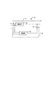
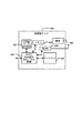
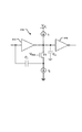
[0060]次に図3Aを参照する。この図は、本発明による補償付きの増幅器回路50の電気回路図を示している。増幅器回路の特定の実施例を示して説明するが、その他の組み合わせも考えられる。増幅器回路50は、入力及び出力を有する第1の増幅器モジュール52を含む。増幅器モジュール52の入力は、増幅器モジュール55の入力に接続している。増幅器モジュール55の出力は、キャパシタ56によって増幅器モジュール52の出力に接続されている。
[0060] Reference is now made to FIG. This figure shows an electrical circuit diagram of an
[0061]増幅器モジュール55は、増幅器52の利得より小さい利得を有していてもよい。増幅器モジュール52は、100以上の利得を有していてもよい。増幅器モジュール55は、100未満の利得を有していてもよい。幾つかの実装形態では、増幅器モジュール55の利得は、実質的に100未満である。増幅器モジュール55は、非常に大きい帯域幅及び小さい出力インピーダンスを有していてもよい。増幅器モジュール55は、増幅器モジュール52の帯域幅より大きい帯域幅を有する。増幅器モジュール52の出力インピーダンスは、増幅器モジュール55の出力インピーダンスより大きくてもよい。増幅器モジュール55は、トランスインピーダンス増幅器を含んでいてもよい。増幅器回路50は、第1のDCパス57及び第2の高周波パス58を有している。
[0061] The
[0062]次に図3B〜3Dを参照する。増幅器の種々の組み合わせを、増幅器回路50の増幅器モジュール52及び55に使用することが可能である。特定の実施例が示されているが、その他の組み合わせも考えられる。図3Bでは、増幅器モジュール52は、増幅器53を含んでいてもよい。図3Cでは、増幅器モジュール55は、トランスインピーダンス増幅器を含んでいてもよい。図3Dでは、増幅器モジュール52は、ミラー補償増幅器を含んでいてもよい。更に別の変形態様も考えられる。
[0062] Reference is now made to FIGS. Various combinations of amplifiers can be used for the
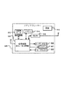
[0063]図3Cを再び参照する。増幅器回路50は、増幅器モジュール52を含んでおり、このモジュール52は、第1の増幅器53を含んでおり、当該第1の増幅器53は、第2の増幅器54の入力に接続する出力を有している。増幅器53の入力は、増幅器モジュール55に接続している。増幅器モジュール55は、増幅器62、増幅器66、及びフィードバック抵抗70を含んでいる。増幅器62の出力は、増幅器66の入力に接続されている。フィードバック抵抗70は、増幅器66の入力と増幅器66の出力との間に接続されている。容量素子56は、増幅器66の出力を増幅器54の入力に容量的に接続している。増幅器53及び54は、DC利得パス80を提供する。DC利得パス80の利得は、追加の増幅器を使用して調整可能である。増幅器62及び66、並びにキャパシタ56は、高周波利得パス84を提供する。
[0063] Referring back to FIG. 3C. The
[0064]次に、図3Dを参照する。増幅器モジュール52は、増幅器53と、容量性フィードバックCMを有するミラー補償増幅器85と、を含んでいてもよい。追加の増幅器86は、ミラー補償増幅器85の出力と増幅器54の入力との間に設けられている。更に別の組み合わせも考えられる。
[0064] Reference is now made to FIG.
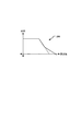
[0065]次に、図4A〜4Cを参照する。これらの図は、増幅器回路の利得及び帯域幅を説明する例示的なグラフを示している。理解できるように、図3Aにおける増幅器回路50は、更なる帯域幅をより高い利得値で有している。利得の傾きは、40dB/decadeに増加されており、これによって、利得が、後に、しかしより急速に低下する。追加の利得ステージは、傾きを60dB/decadeに、図4Bに示されるように、更に増加させる。ステージ及び/又は構造次第では、利得帯域幅応答の領域は、図4Cに示されるように、20、40、60dB/decade等の傾きを有することがある。
[0065] Reference is now made to FIGS. These figures show exemplary graphs illustrating the gain and bandwidth of the amplifier circuit. As can be seen, the
[0066]次に、図5及び6を参照する。これらの図は、補償及び追加の利得付きの別の増幅器の電気回路図を示している。1台以上の追加の増幅器をDC利得パス80に設けて、更なる利得を提供してもよい。図5では、増幅器回路90は、増幅器53及び101を含んでおり、当該増幅器53及び101は、増幅器90の入力と増幅器54との間に接続されている。図6では、増幅器回路100は、一以上の追加の増幅器101−Mを含んでおり、当該増幅器101−Mは、増幅器52−2と54との間に接続されている。なお、Mは1より大きい整数である。理解できるように、追加の増幅器ステージをDCパスに追加して、必要に応じて更なる利得を提供してもよい。
[0066] Reference is now made to FIGS. These figures show the electrical schematic of another amplifier with compensation and additional gain. One or more additional amplifiers may be provided in the
[0067]本発明による増幅器回路は、低周波数と高周波数の両者で利得を向上し、整定時間を向上している。増幅器回路は、各ステージを非カスコード構成にすることができるので、低電圧で動作しながら高利得を有している。 [0067] The amplifier circuit according to the present invention improves gain at both low and high frequencies and improves settling time. The amplifier circuit can have a non-cascode configuration for each stage, and thus has a high gain while operating at a low voltage.
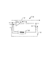
[0068]次に、図7A及び7Bを参照する。増幅器回路108は、入力と、増幅器114の入力に接続された出力とを有する増幅器110を含んでいる。増幅器110の入力は、キャパシタ116によって増幅器118の入力に接続されている。増幅器118の出力は、増幅器120の入力に接続されている。増幅器120の出力は、キャパシタ122によって増幅器114の入力に接続されている。
[0068] Reference is now made to FIGS. 7A and 7B.
[0069]フィードバック抵抗124は、増幅器120の入力と出力に接続されている。フィードバック抵抗126は、増幅器118の入力と出力に接続されている。フィードバック抵抗126は、高抵抗値を有していてもよい。例えば、このフィードバック抵抗は、抵抗124の抵抗値より高い抵抗値を有していてもよい。フィードバック抵抗126は、非常に高い抵抗、例えば、略無限大に近い抵抗を有していてもよい。負荷キャパシタ128を、増幅器114の出力に接続してもよい。図7Bでは、比較的高いフィードバック抵抗128に関連した寄生容量129が、回路の帯域幅を制限する傾向がある。
[0069] The
[0070]図7Cに、本発明による増幅器回路130を示す。増幅器回路130は、スイッチドキャパシタを備えて、寄生容量に伴う問題無しに高フィードバック抵抗126をシミュレートしてもよい。増幅器回路130は、増幅器114の入力に接続された出力を有する増幅器110を備えている。増幅器110の入力は、キャパシタ116によって増幅器118の入力にも接続されている。増幅器118の出力は、増幅器120の入力に接続されている。増幅器120の出力は、キャパシタ122によって増幅器114の入力に接続されている。
[0070] FIG. 7C illustrates an
[0071]増幅器118の入力及び出力は、スイッチドキャパシタ回路131に接続していてもよい。スイッチドキャパシタ回路131は、第1のスイッチ132及び第2のスイッチ134を有している。キャパシタ136は、スイッチ132及び134と、グランドのような基準電位との間に接続されている。第1のフェーズΦ1の間に、第1のスイッチ132が閉じられ、第2のスイッチ134が開かれて、キャパシタ136が充電される。第2のフェーズΦ2の間に、第1のスイッチ132が開かれ、第2のスイッチ134が閉じられ、これによってキャパシタ136を放電させる。第1及び第2のフェーズは、スイッチド入力の第1及び第2のフェーズに対応し、及び/又は、その逆に対応していてもよい。フィードバック抵抗124は、増幅器120の入力と出力に接続されている。負荷キャパシタ146を増幅器114の出力に接続してもよい。幾つかの用途では、増幅器130はスイッチド入力を受けてもよい。スイッチド入力は、容量性ADC、DAC、フィルタなどに見られるようなスイッチドキャパシティブ入力であってもよい。
[0071] The input and output of the
[0072]次に、図8及び9を参照する。これらの図は、スイッチドキャパシタ回路148と図7Cの増幅器130とを備える例示的な回路を示している。増幅器回路130への入力電圧は、スイッチドキャパシティブ入力であってもよい。スイッチドキャパシティブ入力は、フィルタ、デジタル・アナログ変換器(DAC)、アナログ・デジタル変換器(ADC)、及びその他の回路のような回路において生成されてもよい。理解できるように、その他のタイプの入力及び/又は他のスイッチドキャパシタ回路を使用してもよい。スイッチドキャパシタ回路148は、第1のスイッチ152及び第2のスイッチ154を有している。キャパシタ158は、スイッチ152及び154と、グランドのような基準電位との間に接続されている。第1のフェーズΦ1の間に、第1のスイッチ152が閉じられ、第2のスイッチ154が開かれて、キャパシタ158が充電される。第2のフェーズΦ2の間に、第1のスイッチ152が開かれ、第2のスイッチ154が閉じられて、キャパシタ158が増幅器100を介して放電する。
[0072] Reference is now made to FIGS. These figures illustrate an exemplary circuit comprising the switched
[0073]次に、図10を参照する。増幅器回路180は、図7Cに示した増幅器回路と類似しており、増幅器182−1、182−2、...、182−Xを更に備えている。ここで、Xはゼロより大きい整数である。追加の増幅器182は、図4に示した領域200における利得帯域幅応答の傾きを増加させる傾向がある。
[0073] Reference is now made to FIG.
[0074]上記の増幅器回路は、いずれも差動モードで構成することが可能である。例えば、ここで図11を参照すると、図7Cの増幅器が差動モードで構成されている。本明細書に記載されているその他の増幅器も同様に差動モードで構成してもよい。同図は、差動スイッチド入力を受ける本発明による増幅器202を示している。増幅器202は、差動増幅器110Dを備えており、当該増幅器110Dは、差動増幅器114Dの差動入力に接続された差動出力を有している。差動増幅器110Dの差動入力は、キャパシタ116−1及び116−2によって差動増幅器118Dの差動入力に更に接続されている。差動増幅器118Dの差動出力は、差動増幅器120Dの差動入力に接続されている。差動増幅器120Dの差動出力は、キャパシタ122−1及び122−2によって差動増幅器114Dの差動入力に接続されている。
[0074] Any of the above amplifier circuits can be configured in a differential mode. For example, referring now to FIG. 11, the amplifier of FIG. 7C is configured in a differential mode. Other amplifiers described herein may be similarly configured in differential mode. The figure shows an
[0075]差動増幅器118Dの差動入力及び差動出力は、スイッチドキャパシタ回路131−1及び131−2に接続している。負荷キャパシタ(図示せず)を、差動増幅器114Dの差動出力に接続してもよい。
[0075] The differential input and differential output of the
[0076]本明細書で説明した増幅器は、増幅器、演算増幅器、演算トランスコンダクタンス増幅器(OTA)、ミラー補償付き増幅器、及び/又は、その他の適当な増幅器であってもよい。OTAはトランスコンダクタンスタイプのデバイスである。入力電圧は、トランスコンダクタンスgmに基づいて出力電流を制御する。換言すると、OTAは電圧制御型電流源(VCCS)であり、電圧制御型電圧源(VCVS)である従来型の増幅器(オペアンプ)とは著しく異なる。 [0076] The amplifiers described herein may be amplifiers, operational amplifiers, operational transconductance amplifiers (OTAs), Miller compensated amplifiers, and / or other suitable amplifiers. OTA is a transconductance type device. Input voltage controls an output current based on the transconductance g m. In other words, OTA is a voltage controlled current source (VCCS), which is significantly different from a conventional amplifier (op amp) that is a voltage controlled voltage source (VCVS).
[0077]OTAのトランスコンダクタンスパラメータは、増幅器バイアス電流によって制御される。この制御されたトランスコンダクタンスから、出力電流は、入力ピンの間の印加電圧差の関数になる。OTAと従来型のオペアンプとの間には二つの主要な相違点がある。第一に、OTAは電流源であるので、装置の出力インピーダンスが高い。その一方、オペアンプの出力インピーダンスは非常に低い。第二に、OTAを使用して、負フィードバックを利用しない回路を設計することが可能である。換言すると、装置パラメータに対する回路の性能の感度を下げるためにフィードバックを利用しない。 [0077] The transconductance parameter of the OTA is controlled by the amplifier bias current. From this controlled transconductance, the output current is a function of the applied voltage difference between the input pins. There are two major differences between OTA and conventional op amps. First, since OTA is a current source, the output impedance of the device is high. On the other hand, the output impedance of the operational amplifier is very low. Second, it is possible to design a circuit that does not utilize negative feedback using OTA. In other words, no feedback is used to reduce the sensitivity of the circuit performance to device parameters.
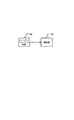
[0078]次に、図12A〜12Gを参照する。これらの図は、本発明の種々の例示的な実装形態を示している。ここで、図12Aを参照する。本発明を、ハードディスクドライブ400内の増幅器、ADC、DAC、フィルタ及びその他の回路に実装することが可能である。幾つかの実装形態では、HDD400内の信号処理及び/又は制御回路402、及び/又は、その他の回路(図示せず)は、データを処理し、符号化及び/又は暗号化を実行し、計算を実行し、並びに/若しくは、磁気記憶媒体406へ出力され、及び/又は、磁気記憶媒体406から入力されるデータをフォーマット化する。
[0078] Reference is now made to FIGS. These figures illustrate various exemplary implementations of the present invention. Reference is now made to FIG. The present invention can be implemented in amplifiers, ADCs, DACs, filters and other circuits within the
[0079]HDD400は、一以上の有線又は無線通信リンク408を介して、コンピュータ、携帯情報端末のような携帯型計算装置、携帯電話機、メディア又はMP3プレーヤー等のようなホスト装置(図示せず)、及び/又は、その他の装置と通信する。HDD400は、例えば、ランダムアクセスメモリ(RAM)、フラッシュメモリのような低遅延の不揮発性メモリ、リードオンリーメモリ(ROM)、及び/又は、その他の適当な電子データ記憶装置などのメモリ409に接続される。
[0079]
[0080]次に、図12Bを参照する。本発明を、デジタル多用途ディスク(DVD)ドライブ410の増幅器、ADC、DAC、フィルタ及びその他の回路において実装することが可能である。信号処理及び/又は制御回路412、及び/又は、DVD410内のその他の回路(図示せず)は、データを処理し、符号化及び/又は暗号化を実行し、計算を実行し、及び/又は、光記憶媒体416へ出力され、及び/又は、磁気記憶媒体416から入力されるデータをフォーマット化する。幾つかの実装形態では、信号処理及び/又は制御回路412、及び/又は、DVD410内のその他の回路(図示せず)は、符号化及び/又は復号化、並びに/若しくは、DVDドライブに関連した任意の別の信号処理機能のようなその他の機能を更に実行する。
[0080] Reference is now made to FIG. The present invention can be implemented in amplifiers, ADCs, DACs, filters and other circuits of a digital versatile disc (DVD)
[0081]DVDドライブ410は、コンピュータ、テレビ、又は、その他の装置のような出力装置(図示せず)と、一以上の有線又は無線通信リンク417を介して、通信してもよい。DVD410は、不揮発性方式でデータを記憶する大容量記憶装置418と通信してもよい。大容量記憶装置418は、ハードディスクドライブ(HDD)を含む。HDDは図12Aに示された構造を有していてもよい。HDDは、約1.8インチより小さい直径を有する1枚以上のプラッタを含むミニHDDであってもよい。DVD410は、例えば、RAM、ROM、フラッシュメモリのような低遅延の不揮発性メモリ、及び/又は、その他の適当な電子データ記憶装置などのメモリ419に接続されてもよい。
[0081] The
[0082]次に、図12Cを参照する。本発明を、高精細テレビ(HDTV)420の増幅器、ADC、DAC、フィルタ及びその他の回路において実装することが可能である。HDTV420は、有線又は無線のいずれかのフォーマットでHDTV入力信号を受信し、ディスプレイ428のためのHDTV出力信号を生成する。幾つかの実装形態では、信号処理回路及び/又は制御回路422、及び/又は、HDTV420のその他の回路(図示せず)は、データを処理し、符号化及び/又は暗号化を実行し、計算を実行し、データをフォーマット化し、並びに/若しくは、要求され得るその他のタイプのHDTV処理を実行してもよい。
[0082] Reference is now made to FIG. The invention can be implemented in high definition television (HDTV) 420 amplifiers, ADCs, DACs, filters and other circuits. The
[0083]HDTV420は、光及び/又は磁気記憶装置のような不揮発性方式でデータを記憶する大容量データ記憶装置427と通信してもよい。少なくとも1台のHDDは図12Aに示された構造を有していてもよく、及び/又は、少なくとも1台のDVDは図12Bに示された構造を有していてもよい。HDDは、約1.8インチより小さい直径を有する1枚以上のプラッタを含むミニHDDでもよい。HDTV420は、例えば、RAM、ROM、フラッシュメモリのような低遅延の不揮発性メモリ、及び/又は、その他の適当な電子データ記憶装置などのメモリ428に接続されてもよい。HDTV420は、WLANネットワークインターフェイス429を介してWLANとの接続もサポートしてもよい。
[0083] The
[0084]次に、図12Dを参照する。本発明は、車両430の制御システムの増幅器、ADC、DAC、フィルタ、及びその他の回路、WLANインターフェイス、車両制御システムの大容量データ記憶装置、並びに/若しくは、電源433において、実装してもよく、及び/又は、それらにおいて実施されてもよい。幾つかの実装形態では、本発明は、パワートレイン制御システム432を実施する。パワートレイン制御システム432は、温度センサ、圧力センサ、回転センサ、気流センサ、及び/又は、その他の適当なセンサのような1台以上のセンサから入力を受信し、及び/又は、エンジン動作パラメータ、伝達動作パラメータ、及び/又は、その他の制御信号のような一以上の出力制御信号を生成するする。
[0084] Reference is now made to FIG. The present invention may be implemented in amplifiers, ADCs, DACs, filters, and other circuits in a
[0085]本発明を、車両430のその他の制御システム440において実装してもよい。制御システム440も同様に、入力センサ442から信号を受信してもよく、一以上の出力装置444へ制御信号を出力してもよい。幾つかの実装形態では、制御システム440は、アンチロックブレーキングシステム(ABS)と、ナビゲーションシステムと、テレマティックスシステムと、車両テレマティックスシステムと、車線離脱システムと、適応クルーズ制御システムと、ステレオ、DVD、コンパクトディスクなどのような車両エンターテイメントシステムの一部分であってもよい。更に別の実装形態も考えられる。
[0085] The present invention may be implemented in
[0086]パワートレイン制御システム432は、不揮発性方式でデータを記憶する大容量データ記憶装置446と通信してもよい。大容量データ記憶装置446は、例えば、ハードディスクドライブHDD及び/又はDVDのような光及び/又は磁気ディスク記憶装置を含んでもよい。少なくとも1台のHDDは図12Aに示された構造を有していてもよく、及び/又は、少なくとも1台のDVDは図12Bに示された構造を有していてもよい。HDDは、約1.8インチより小さい直径を有する1枚以上のプラッタを含むミニHDDであってもよい。パワートレイン制御システム432は、例えば、RAM、ROM、フラッシュメモリのような低遅延の不揮発性メモリ、及び/又は、その他の適当な電子データ記憶装置などのメモリ447に接続されてもよい。パワートレイン制御システム432は、WLANネットワークインターフェイス448を介してWLANとの接続もサポートしてもよい。制御システム440は、また、大容量データ記憶装置、メモリ、及び/又は、WLANインターフェイス(すべて図示されていない)を更に備えてもよい。
[0086] The
[0087]次に、図12Eを参照する。本発明を、セルラーアンテナ451を含み得る携帯電話機450の増幅器、ADC、DAC、フィルタ、及びその他の回路において実装することができる。幾つかの実装形態では、携帯電話機450は、マイクロホン456、スピーカー及び/又はオーディオ出力ジャックのようなオーディオ出力458、ディスプレイ460、並びに/若しくは、キーパッド、ポインティングデバイス、音声作動及び/又はその他の入力装置のような入力装置462を含む。信号処理及び/又は制御回路452、及び/又は、携帯電話機450内のその他の回路(図示せず)は、データを処理し、符号化及び/又は暗号化を実行し、計算を実行し、データをフォーマット化し、及び/又は、その他の携帯電話機能を実行してもよい。
[0087] Reference is now made to FIG. The present invention can be implemented in amplifiers, ADCs, DACs, filters, and other circuits of a
[0088]携帯電話機450は、例えば、ハードディスクドライブHDD及び/又はDVDといった光及び/又は磁気ディスク記憶装置のような不揮発性方式でデータを記憶する大容量データ記憶装置464と通信してもよい。少なくとも1台のHDDは図12Aに示された構造を有し、及び/又は、少なくとも1台のDVDは図12Bに示された構造を有していてもよい。HDDは、約1.8インチより小さい直径を有する1枚以上のプラッタを含むミニHDDであってもよい。携帯電話機450は、例えば、RAM、ROM、フラッシュメモリのような低遅延の不揮発性メモリ、及び/又は、その他の適当な電子データ記憶装置などのメモリ466に接続されてもよい。携帯電話機450は、また、WLANネットワークインターフェイス468を介してWLANとの接続をサポートしてもよい。
[0088] The
[0089]次に、図12Fを参照する。本発明を、セットトップボックス480の増幅器、ADC、DAC、フィルタ、及びその他の回路において実装してもよい。セットトップボックス480は、ブロードバンドソースのようなソースから信号を受信し、テレビ、及び/又は、モニタ、並びに/若しくは、その他のビデオ及び/又はオーディオ出力装置といったディスプレイ488に適した標準、及び/又は、高精細のオーディオ/ビデオ信号を出力する。信号処理及び/又は制御回路484、及び/又は、セットトップボックス480内のその他の回路(図示せず)は、データを処理し、符号化及び/又は暗号化を実行し、計算を実行し、データをフォーマット化し、及び/又は、その他のセットトップボックス機能を実行してもよい。
[0089] Reference is now made to FIG. The present invention may be implemented in amplifiers, ADCs, DACs, filters, and other circuits of set
[0090]セットトップボックス480は、不揮発性方式でデータを記憶する大容量データ記憶装置490と通信してもよい。大容量データ記憶装置490は、例えば、ハードディスクドライブHDD及び/又はDVDのような光及び/又は磁気ディスク記憶装置を含んでもよい。少なくとも1台のHDDは図12Aに示された構造を有し、及び/又は、少なくとも1台のDVDは図12Bに示された構造を有していてもよい。HDDは、約1.8インチより小さい直径を有する1枚以上のプラッタを含むミニHDDであってもよい。セットトップボックス480は、例えば、RAM、ROM、フラッシュメモリのような低遅延の不揮発性メモリ、及び/又は、その他の適当な電子データ記憶装置などのメモリ4124に接続されていてもよい。セットトップボックス480は、また、WLANネットワークインターフェイス4126を介してWLANとの接続をサポートしてもよい。
[0090] Set
[0091]次に、図12Gを参照する。本発明を、メディアプレーヤー500の増幅器、ADC、DAC、フィルタ、及びその他の回路において実装することが可能である。幾つかの実装形態では、メディアプレーヤー500は、ディスプレイ507、及び/又は、キーパッド、タッチパッドなどのユーザ入力508を含む。幾つかの実装形態では、メディアプレーヤー500は、グラフィカルユーザインターフェイス(GUI)を採用してもよい。GUIは、通常、ディスプレイ507及び/又はユーザ入力508を介するメニュー、ドロップダウンメニュー、アイコン、及び/又は、ポイントアンドクリックインターフェイスを採用する。メディアプレーヤー500は、スピーカー及び/又はオーディオ出力ジャックのようなオーディオ出力509を更に含む。信号処理及び/又は制御回路504、及び/又は、メディアプレーヤー500のその他の回路(図示せず)は、データを処理し、符号化及び/又は暗号化を実行し、計算を実行し、データをフォーマット化し、及び/又は、その他のメディアプレーヤー機能を実行してもよい。
[0091] Reference is now made to FIG. The present invention may be implemented in
[0092]メディアプレーヤー500は、圧縮オーディオ及び/又はビデオコンテンツのようなデータを不揮発性方式で記憶する大容量データ記憶装置510と通信してもよい。幾つかの実装形態では、圧縮オーディオファイルは、MP3フォーマット、及び/又は、その他の適当な圧縮オーディオ及び/又はビデオフォーマットに準拠したファイルを含む。大容量データ記憶装置は、例えば、ハードディスクドライブHDD及び/又はDVDのような光及び/又は磁気ディスク記憶装置を含んでいてもよい。少なくとも1台のHDDは図12Aに示された構造を有し、及び/又は、少なくとも1台のDVDは図12Bに示された構造を有していてもよい。HDDは、約1.8インチより小さい直径を有する1枚以上のプラッタを含むミニHDDであってもよい。メディアプレーヤー500は、例えば、RAM、ROM、フラッシュメモリのような低遅延の不揮発性メモリ、及び/又は、その他の適当な電子データ記憶装置などのメモリ514に接続されていてもよい。メディアプレーヤー500は、また、WLANネットワークインターフェイス516を介してWLANとの接続をサポートしてもよい。上記の実装形態に加えて、更に他の実装形態も考えられる。
[0092] The
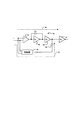
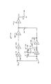
[0093]次に、図13を参照する。この図は、補償付きの別の代替的な増幅器システム610の電気回路図を示している。増幅器システム610は、第1の増幅器ステージ614と、第2の増幅器ステージ616と、を含んでいる。第1の増幅器ステージ614の入力は、第1のキャパシタCcの一端に接続している。増幅器ステージ614の出力は、第2の増幅器ステージ616の入力に接続されている。
[0093] Reference is now made to FIG. This figure shows an electrical schematic of another
[0094]第1のトランジスタT1の第1の端子は、第1の増幅器ステージ614の出力に接続されている。トランジスタT1の第2の端子は、第1のキャパシタCcの他端及び電流源I2に接続されている。別の電流源I1は、第1の増幅器ステージ614の出力に接続されている。電流源I1は、第1の電圧基準Vddに接続していてもよい。寄生容量Cpが、第2の増幅器ステージ616の入力に存在する。電圧バイアスVbiasは、ランジスタT1の制御端子へ入力される。
[0094] The first terminal of the first transistor T1 is connected to the output of the
[0095]増幅器ステージ614及び618の一方は反転増幅器であってもよい。電流源I1及びI2は、それぞれ、実質的に等しい電流の大きさのソース及びシンクを行ってもよい。トランジスタT1は、CMOSトランジスタであってもよく、その他の適当なトランジスタであってもよい。増幅器の実効利得は、Cc/Cpに略等しい。図13の増幅器システム610は、フィードフォワード利得付きの類似の増幅器より高い帯域幅と低い雑音を有する傾向がある。この回路は、共通ゲート電流増幅器構造で構成されている。
[0095] One of the amplifier stages 614 and 618 may be an inverting amplifier. Current sources I 1 and I 2 may source and sink substantially the same current magnitude, respectively. Transistor T1 may be a CMOS transistor or any other suitable transistor. The effective gain of the amplifier is approximately equal to C c / C p . The
[0096]次に、図14を参照する。この図は、図13の増幅器の例示的な利得及び帯域幅を説明するグラフを示している。増幅器システム610は、上述した利得及び帯域幅と類似した利得/帯域幅特性を有する。
[0096] Reference is now made to FIG. This figure shows a graph illustrating exemplary gain and bandwidth of the amplifier of FIG.
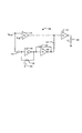
[0097]次に、図15A及び15Bを参照する。これらの図は、補償付きのその他の代替的な増幅器システム650の電気回路図を示している。図15Aでは、増幅器システム650が、第1の増幅器ステージ654及び第2の増幅器ステージ656を備えている。第1の増幅器ステージ654の入力は、第1のキャパシタCc1の一端に接続している。増幅器ステージ654の出力は、第2の増幅器ステージ656の入力に接続されている。
[0097] Reference is now made to FIGS. 15A and 15B. These figures show an electrical schematic of another
[0098]トランジスタT1の第2の端子は、第1のキャパシタCc1の他端及び抵抗Rに接続されている。トランジスタT1の第1の端子は、電流源I2、及びキャパシタCc2の一端に接続している。キャパシタCc2の他端は、第1の増幅器ステージ654の出力、及び第2の増幅器ステージ656の入力に接続している。別の電流源I1は第1の増幅器ステージ654の出力に接続されている。寄生容量Cpが、第2の増幅器ステージ656の入力に存在する。
[0098] The second terminal of the transistor T1 is connected to the other end of the first capacitor Cc1 and the resistor R. The first terminal of the transistor T1 is connected to the current source I 2 and one end of the capacitor C c2 . The other end of the capacitor C c2 is connected to the output of the
[0099]増幅器システム650は、電流源I1及びI2が等しい電流レベルを提供しない場合に生じる問題に対処可能である。トランジスタT1の第1の端子は、電流源I2に接続されており、第1の増幅器ステージ654の出力及び第2の増幅器ステージ656の入力に容量的に接続されている。第1の電圧基準Vdd及び第2の電圧基準Vは、実質的に等しい電圧基準であっても、又は、異なる電圧基準であってもよい。高周波では、この増幅器システムの利得は、図13の増幅器システムに類似する。
[0099] The
[0100]図15Bは、代替の適切な構成を示している。抵抗Rと電流源I2の相対的な位置は、図15Aに示されたものの逆である。換言すると、抵抗Rの一端は電圧基準Vに接続しており、抵抗Rの反対端はトランジスタT1の第1の端子及びキャパシタCc2に接続している。電流源I2は、トランジスタT1の第2の端子及びキャパシタCc1の他端に接続している。 [0100] FIG. 15B illustrates an alternative suitable configuration. The relative positions of the resistor R and the current source I 2 is the reverse of those shown in Figure 15A. In other words, one end of the resistor R is connected to the voltage reference V, and the other end of the resistor R is connected to the first terminal of the transistor T1 and the capacitor Cc2 . Current source I 2 is connected to the other end of the second terminal and the capacitor C c1 of the transistor T1.
[0101]本明細書で説明した増幅器は、増幅器、演算増幅器、演算トランスコンダクタンス増幅器(OTA)、ミラー補償付き増幅器、及び/又は、その他の適当な増幅器であってもよい。 [0101] The amplifiers described herein may be amplifiers, operational amplifiers, operational transconductance amplifiers (OTAs), Miller compensated amplifiers, and / or other suitable amplifiers.
[0101]当業者は、以上の説明から、本発明の広い教示を種々の態様で実施し得ることを認識できる。したがって、本発明を特定の実施例との関連において説明したが、図面、明細書、及び特許請求の範囲を詳しく検討することによって、その他の変更が当業者に明白になるので、本発明の真の範囲はそのように限定されるべきではない。 [0101] Those skilled in the art can now appreciate from the foregoing description that the broad teachings of the present invention can be implemented in a variety of forms. Thus, while the present invention has been described in connection with specific embodiments, other modifications will become apparent to those skilled in the art upon detailed review of the drawings, specification, and claims. The scope of should not be so limited.
10,50,90,100,108,130,180…増幅器回路、14,16,53、62,66,101、101−M,110,114,118,120、182−1,182−2,182−X,202…増幅器、18…ミラー容量、52,55…増幅器モジュール、56,116,116−1,116−2,122,122−1,122−2,158…キャパシタ、57…第1のDCパス、58…第2の高周波パス、70,124,126…フィードバック抵抗、80…DC利得パス、84…高周波利得パス、85…ミラー補償増幅器、110D,114D,118D,120D…差動増幅器、128,146…負荷容量、129…寄生容量、131,131−1,131−2,148…スイッチドキャパシタ回路、132,134,152,154…スイッチ、200…領域、400…ハードディスクドライブ、402,412,422,452,484,504…信号処理及び/又は制御回路、406…磁気記憶媒体、408,417…通信リンク、409,419,428,447,466,494,514…メモリ、410…デジタル多用途ディスク、416…光記憶媒体、418…大容量記憶装置、420…高精細テレビ、426,460,488,507…ディスプレイ、427,446,464,490,510…大容量データ記憶装置、429,448,468,496,516…WLANネットワークインターフェイス、430…車両、432…パワートレイン制御システム、440…その他の制御システム、442…入力センサ、444…出力装置、450…携帯電話機、451…セルラーアンテナ、456…マイクロホン、458,509…オーディオ出力、462…入力装置、480…セットトップボックス、500…メディアプレーヤー、508…ユーザ入力、610,650…増幅器システム、614,616,654,656…増幅器ステージ。 10, 50, 90, 100, 108, 130, 180 ... amplifier circuit, 14, 16, 53, 62, 66, 101, 101-M, 110, 114, 118, 120, 182-1, 182-2, 182 -X, 202 ... amplifier, 18 ... mirror capacitance, 52, 55 ... amplifier module, 56, 116, 116-1, 116-2, 122, 122-1, 122-2, 158 ... capacitor, 57 ... first DC path, 58 ... second high frequency path, 70, 124, 126 ... feedback resistor, 80 ... DC gain path, 84 ... high frequency gain path, 85 ... Miller compensation amplifier, 110D, 114D, 118D, 120D ... differential amplifier, 128, 146 ... load capacitance, 129 ... parasitic capacitance, 131, 131-1, 131-2, 148 ... switched capacitor circuit, 132, 134, 52,154 ... switch, 200 ... area, 400 ... hard disk drive, 402,412,422,452,484,504 ... signal processing and / or control circuit, 406 ... magnetic storage medium, 408,417 ... communication link, 409, 419, 428, 447, 466, 494, 514 ... Memory, 410 ... Digital versatile disc, 416 ... Optical storage medium, 418 ... Mass storage device, 420 ... High definition television, 426, 460, 488, 507 ... Display, 427, 446, 464, 490, 510 ... Mass data storage devices, 429, 448, 468, 496, 516 ... WLAN network interface, 430 ... Vehicle, 432 ... Powertrain control system, 440 ... Other control systems, 442 ... Input sensor, 444... Output device, 4 DESCRIPTION OF SYMBOLS 0 ... Mobile phone, 451 ... Cellular antenna, 456 ... Microphone, 458, 509 ... Audio output, 462 ... Input device, 480 ... Set top box, 500 ... Media player, 508 ... User input, 610, 650 ... Amplifier system, 614 , 616, 654, 656... Amplifier stage.
Claims (6)
前記第1の増幅器の前記出力に接続する入力を有する第2の増幅器と、
第1端及び第2端を有する第1のキャパシタであって、該第1のキャパシタの該第1端は前記第1の増幅器の前記入力に接続する、該第1のキャパシタと、
第1端及び第2端を有する第2のキャパシタであって、該第2のキャパシタの該第1端は前記第1の増幅器の前記出力に接続する、該第2のキャパシタと、
第1端及び第2端を有する抵抗であって、該抵抗の該第1端は第1の電圧源に接続されており、該抵抗の該第2端は前記第2のキャパシタの前記第2端に接続されている、該抵抗と、
制御端子、前記抵抗の前記第2端及び前記第2のキャパシタの前記第2端に接続する第1の端子、並びに、前記第1のキャパシタの前記第2端に接続する第2の端子を有する第1のトランジスタと、
入力及び出力を有する電流源であって、該電流源の該入力は前記第1のキャパシタの前記第2端及び前記第1のトランジスタの前記第2の端子に接続されており、該電流源の該出力は電圧基準に接続されている、該電流源と、
を備え、
前記第1のトランジスタは、前記第1のキャパシタと前記第1の増幅器の出力との間に接続されている、増幅器システム。 A first amplifier having (i) an input configured to receive an input signal and (ii) an output configured to receive a supply voltage from a voltage source;
A second amplifier having an input connected to the output of the first amplifier;
A first capacitor having a first end and a second end, wherein the first end of the first capacitor is connected to the input of the first amplifier;
A second capacitor having a first end and a second end, wherein the second capacitor is connected to the output of the first amplifier;
A resistor having a first end and a second end, wherein the first end of the resistor is connected to a first voltage source, and the second end of the resistor is the second end of the second capacitor. The resistor connected to the end; and
A control terminal, a first terminal connected to said second end of said second end of the resistor and said second capacitor, and has a second terminal connected to said second end of said first capacitor A first transistor;
A current source having an input and an output, wherein the input of the current source is connected to the second end of the first capacitor and the second terminal of the first transistor; The output is connected to a voltage reference; the current source;
With
The amplifier system, wherein the first transistor is connected between the first capacitor and an output of the first amplifier.
Applications Claiming Priority (8)
| Application Number | Priority Date | Filing Date | Title |
|---|---|---|---|
| US11/264,921 US7202733B1 (en) | 2005-11-02 | 2005-11-02 | Transconductance amplifiers with compensation |
| US11/264921 | 2005-11-02 | ||
| US79928206P | 2006-05-10 | 2006-05-10 | |
| US60/799282 | 2006-05-10 | ||
| US82087806P | 2006-07-31 | 2006-07-31 | |
| US60/820878 | 2006-07-31 | ||
| US11/503,436 US7459972B2 (en) | 2005-11-02 | 2006-08-11 | Amplifiers with compensation |
| US11/503436 | 2006-08-11 |
Publications (3)
| Publication Number | Publication Date |
|---|---|
| JP2007129720A JP2007129720A (en) | 2007-05-24 |
| JP2007129720A5 JP2007129720A5 (en) | 2009-12-17 |
| JP5010239B2 true JP5010239B2 (en) | 2012-08-29 |
Family
ID=37593827
Family Applications (1)
| Application Number | Title | Priority Date | Filing Date |
|---|---|---|---|
| JP2006299309A Active JP5010239B2 (en) | 2005-11-02 | 2006-11-02 | Compensated amplifier |
Country Status (5)
| Country | Link |
|---|---|
| US (2) | US7459972B2 (en) |
| EP (1) | EP1783894B1 (en) |
| JP (1) | JP5010239B2 (en) |
| SG (1) | SG131904A1 (en) |
| TW (1) | TWI426704B (en) |
Families Citing this family (14)
| Publication number | Priority date | Publication date | Assignee | Title |
|---|---|---|---|---|
| US7551024B2 (en) * | 2001-03-13 | 2009-06-23 | Marvell World Trade Ltd. | Nested transimpedance amplifier |
| US7558014B1 (en) | 2004-06-24 | 2009-07-07 | Marvell International Ltd. | Programmable high pass amplifier for perpendicular recording systems |
| JP5407264B2 (en) * | 2008-10-09 | 2014-02-05 | ソニー株式会社 | Solid-state imaging device and camera system |
| US8385016B1 (en) * | 2009-11-04 | 2013-02-26 | Marvell International, Inc. | Asymmetric correction circuit |
| EP3145216B1 (en) * | 2015-09-17 | 2018-11-14 | Nxp B.V. | Amplifier system |
| JP2017079397A (en) * | 2015-10-20 | 2017-04-27 | 株式会社東芝 | Amplifier circuit |
| US9667351B2 (en) | 2015-10-30 | 2017-05-30 | Avago Technologies General Ip (Singapore) Pte. Ltd. | Simultaneous bandwidth extension at high gain and peaking reduction at minimum gain for wideband, variable gain, linear optical receivers |
| US10469037B2 (en) | 2017-04-19 | 2019-11-05 | Mediatek Inc. | Multi-stage amplifier circuit with zero and pole inserted by compensation circuits |
| US10224887B2 (en) | 2017-08-04 | 2019-03-05 | Analog Devices, Inc. | Variable gain-bandwidth transimpedance amplifier |
| CN109428563B (en) * | 2017-08-25 | 2022-11-22 | 瑞昱半导体股份有限公司 | Impedance correction device and method thereof |
| TWI641213B (en) * | 2017-09-05 | 2018-11-11 | 瑞昱半導體股份有限公司 | Amplifier and reset method thereof |
| CN109474241B (en) * | 2017-09-08 | 2022-09-27 | 瑞昱半导体股份有限公司 | Amplifier and reset method thereof |
| CN111478671B (en) * | 2020-04-13 | 2023-04-14 | 电子科技大学 | A Novel Low Noise Amplifier Applied in Sub-GHz Frequency Band |
| EP3945672B1 (en) * | 2020-07-31 | 2025-09-10 | NXP USA, Inc. | Error amplifier circuits for dc-dc converters, dc-dc converters and controllers |
Family Cites Families (31)
| Publication number | Priority date | Publication date | Assignee | Title |
|---|---|---|---|---|
| US3079568A (en) * | 1959-02-09 | 1963-02-26 | Acf Ind Inc | Broad band amplifier |
| US3605031A (en) * | 1969-09-04 | 1971-09-14 | Blonder Tongue Lab | Wide-band low-distortion alternating current amplifier |
| US4185249A (en) * | 1978-08-23 | 1980-01-22 | Hewlett-Packard Company | Bipolar signal to current converter |
| US4405899A (en) * | 1979-03-01 | 1983-09-20 | Motorola, Inc. | High pass filter and method of making same |
| NL8002666A (en) * | 1980-05-09 | 1981-12-01 | Philips Nv | OPERATIONAL AMPLIFIER. |
| NL8204024A (en) * | 1982-10-19 | 1984-05-16 | Philips Nv | OPERATIONAL AMPLIFIER. |
| US4559502A (en) * | 1984-04-19 | 1985-12-17 | Signetics Corporation | Multi-stage amplifier with capacitive nesting for frequency compensation |
| JPH0767052B2 (en) * | 1985-10-24 | 1995-07-19 | 日本電気株式会社 | Phase compensation circuit |
| US5121075A (en) * | 1991-03-04 | 1992-06-09 | Hewlett-Packard Co. | Precision programmable attenuator |
| DE69429212D1 (en) * | 1993-06-21 | 2002-01-10 | Koninkl Philips Electronics Nv | Reinforcement arrangement with multi-way zero suppression |
| AUPN204295A0 (en) * | 1995-03-29 | 1995-04-27 | Hildebrandt, William James | Amplifying circuit |
| DE69529908T2 (en) * | 1995-11-30 | 2003-12-04 | Stmicroelectronics S.R.L., Agrate Brianza | Frequency self-compensated operational amplifier |
| US6002299A (en) * | 1997-06-10 | 1999-12-14 | Cirrus Logic, Inc. | High-order multipath operational amplifier with dynamic offset reduction, controlled saturation current limiting, and current feedback for enhanced conditional stability |
| DE69727934D1 (en) * | 1997-10-31 | 2004-04-08 | St Microelectronics Srl | Integrated power amplifier allowing parallel connections |
| US6114907A (en) * | 1998-12-08 | 2000-09-05 | National Semiconductor Corporation | Amplifier with dynamic compensation and method |
| US6208206B1 (en) * | 1999-02-11 | 2001-03-27 | The Hong Kong University Of Science And Technology | Frequency compensation techniques for low-power multistage amplifiers |
| JP2000261265A (en) * | 1999-03-10 | 2000-09-22 | Toshiba Microelectronics Corp | Feedback variable gain amplifier circuit |
| US6400301B1 (en) * | 2000-09-07 | 2002-06-04 | Texas Instruments Incorporated | amplifying signals in switched capacitor environments |
| US6340916B1 (en) * | 2000-09-21 | 2002-01-22 | Telecommunications Laboratories, Chunghwa Telecom Co., Ltd. | Ransimpedance amplifier circuit |
| US6407640B1 (en) * | 2000-09-22 | 2002-06-18 | Qualcomm, Incorporated | Two-stage LNA with good linearity |
| US6624704B1 (en) * | 2001-10-25 | 2003-09-23 | National Semiconductor Corporation | High speed high current gain operational amplifier |
| US6882226B2 (en) * | 2002-05-16 | 2005-04-19 | Integrant Technologies Inc. | Broadband variable gain amplifier with high linearity and variable gain characteristic |
| US6842068B2 (en) * | 2003-02-27 | 2005-01-11 | Semiconductor Components Industries, L.L.C. | Power management method and structure |
| US6930544B2 (en) * | 2003-03-07 | 2005-08-16 | Matsushita Electric Industrial Co., Ltd. | Filter |
| US7002409B1 (en) * | 2004-02-11 | 2006-02-21 | Marvell International Ltd. | Compensation circuit for amplifiers having multiple stages |
| US7324035B2 (en) * | 2004-05-13 | 2008-01-29 | University Of Florida Research Foundation, Inc. | Amplifier with pulse coded output and remote signal reconstruction from the pulse output |
| TWI237441B (en) * | 2004-11-25 | 2005-08-01 | Himax Tech Inc | Operational amplifier with frequency compensation circuit |
| US7202746B1 (en) * | 2004-12-14 | 2007-04-10 | Cirrus Logic, Inc. | Multiple-stage operational amplifier and methods and systems utilizing the same |
| US7202733B1 (en) | 2005-11-02 | 2007-04-10 | Marvell International Ltd. | Transconductance amplifiers with compensation |
| US7161420B1 (en) | 2005-11-02 | 2007-01-09 | Marvell World Trade Ltd. | Amplifiers with compensation |
| US7199656B1 (en) | 2005-11-02 | 2007-04-03 | Marvell World Trade International | Amplifiers with compensation |
-
2006
- 2006-08-11 US US11/503,436 patent/US7459972B2/en not_active Expired - Lifetime
- 2006-10-25 EP EP06022343.5A patent/EP1783894B1/en not_active Ceased
- 2006-10-30 SG SG200607353-0A patent/SG131904A1/en unknown
- 2006-10-31 TW TW095140239A patent/TWI426704B/en not_active IP Right Cessation
- 2006-11-02 JP JP2006299309A patent/JP5010239B2/en active Active
-
2008
- 2008-12-02 US US12/326,197 patent/US7737777B2/en not_active Expired - Lifetime
Also Published As
| Publication number | Publication date |
|---|---|
| US7737777B2 (en) | 2010-06-15 |
| EP1783894A2 (en) | 2007-05-09 |
| TWI426704B (en) | 2014-02-11 |
| JP2007129720A (en) | 2007-05-24 |
| EP1783894A3 (en) | 2008-07-02 |
| SG131904A1 (en) | 2007-05-28 |
| US20090140803A1 (en) | 2009-06-04 |
| US7459972B2 (en) | 2008-12-02 |
| TW200729699A (en) | 2007-08-01 |
| US20070109057A1 (en) | 2007-05-17 |
| EP1783894B1 (en) | 2019-03-20 |
Similar Documents
| Publication | Publication Date | Title |
|---|---|---|
| US7737777B2 (en) | Amplifiers with compensation | |
| CN1968008B (en) | Amplifiers with compensation | |
| US7760029B2 (en) | High-bandwidth high-gain amplifier | |
| US7696820B1 (en) | Increasing amplifier bandwidth by positive capacitive feedback | |
| TWI433452B (en) | Nested transimpedance amplifier | |
| US7323930B2 (en) | Amplifiers with compensation | |
| US7688141B1 (en) | Multi-amplifier circuit | |
| US7589649B1 (en) | Apparatus, method, and system for correction of baseline wander | |
| US7525347B1 (en) | Differential peak detector | |
| EP1783899B1 (en) | High-bandwidth high-gain amplifier | |
| EP2495872B1 (en) | Two-stage class AB operational amplifier | |
| JP2007129719A (en) | Amplifier with compensation | |
| US7375575B1 (en) | Method and apparatus for controlled voltage level shifting | |
| US7199656B1 (en) | Amplifiers with compensation | |
| US7852123B1 (en) | Reset-free comparator with built-in reference | |
| HK1106344A (en) | Amplifiers with compensation | |
| HK1106879A (en) | Amplifiers with compensation |
Legal Events
| Date | Code | Title | Description |
|---|---|---|---|
| A521 | Request for written amendment filed |
Free format text: JAPANESE INTERMEDIATE CODE: A523 Effective date: 20091029 |
|
| A621 | Written request for application examination |
Free format text: JAPANESE INTERMEDIATE CODE: A621 Effective date: 20091029 |
|
| A977 | Report on retrieval |
Free format text: JAPANESE INTERMEDIATE CODE: A971007 Effective date: 20110209 |
|
| A131 | Notification of reasons for refusal |
Free format text: JAPANESE INTERMEDIATE CODE: A131 Effective date: 20110215 |
|
| A521 | Request for written amendment filed |
Free format text: JAPANESE INTERMEDIATE CODE: A523 Effective date: 20110412 |
|
| A131 | Notification of reasons for refusal |
Free format text: JAPANESE INTERMEDIATE CODE: A131 Effective date: 20110906 |
|
| A521 | Request for written amendment filed |
Free format text: JAPANESE INTERMEDIATE CODE: A523 Effective date: 20111115 |
|
| TRDD | Decision of grant or rejection written | ||
| A01 | Written decision to grant a patent or to grant a registration (utility model) |
Free format text: JAPANESE INTERMEDIATE CODE: A01 Effective date: 20120522 |
|
| A01 | Written decision to grant a patent or to grant a registration (utility model) |
Free format text: JAPANESE INTERMEDIATE CODE: A01 |
|
| A61 | First payment of annual fees (during grant procedure) |
Free format text: JAPANESE INTERMEDIATE CODE: A61 Effective date: 20120601 |
|
| R150 | Certificate of patent or registration of utility model |
Ref document number: 5010239 Country of ref document: JP Free format text: JAPANESE INTERMEDIATE CODE: R150 |
|
| FPAY | Renewal fee payment (event date is renewal date of database) |
Free format text: PAYMENT UNTIL: 20150608 Year of fee payment: 3 |
|
| R250 | Receipt of annual fees |
Free format text: JAPANESE INTERMEDIATE CODE: R250 |
|
| R250 | Receipt of annual fees |
Free format text: JAPANESE INTERMEDIATE CODE: R250 |
|
| R250 | Receipt of annual fees |
Free format text: JAPANESE INTERMEDIATE CODE: R250 |
|
| R250 | Receipt of annual fees |
Free format text: JAPANESE INTERMEDIATE CODE: R250 |
|
| R250 | Receipt of annual fees |
Free format text: JAPANESE INTERMEDIATE CODE: R250 |
|
| S111 | Request for change of ownership or part of ownership |
Free format text: JAPANESE INTERMEDIATE CODE: R313113 |
|
| R250 | Receipt of annual fees |
Free format text: JAPANESE INTERMEDIATE CODE: R250 |
|
| R371 | Transfer withdrawn |
Free format text: JAPANESE INTERMEDIATE CODE: R371 |
|
| S111 | Request for change of ownership or part of ownership |
Free format text: JAPANESE INTERMEDIATE CODE: R313113 |
|
| R360 | Written notification for declining of transfer of rights |
Free format text: JAPANESE INTERMEDIATE CODE: R360 |
|
| S111 | Request for change of ownership or part of ownership |
Free format text: JAPANESE INTERMEDIATE CODE: R313113 |
|
| R360 | Written notification for declining of transfer of rights |
Free format text: JAPANESE INTERMEDIATE CODE: R360 |
|
| R371 | Transfer withdrawn |
Free format text: JAPANESE INTERMEDIATE CODE: R371 |
|
| R350 | Written notification of registration of transfer |
Free format text: JAPANESE INTERMEDIATE CODE: R350 |
|
| S111 | Request for change of ownership or part of ownership |
Free format text: JAPANESE INTERMEDIATE CODE: R313113 |
|
| R350 | Written notification of registration of transfer |
Free format text: JAPANESE INTERMEDIATE CODE: R350 |
|
| R250 | Receipt of annual fees |
Free format text: JAPANESE INTERMEDIATE CODE: R250 |
|
| S111 | Request for change of ownership or part of ownership |
Free format text: JAPANESE INTERMEDIATE CODE: R313113 |
|
| S531 | Written request for registration of change of domicile |
Free format text: JAPANESE INTERMEDIATE CODE: R313531 |
|
| R360 | Written notification for declining of transfer of rights |
Free format text: JAPANESE INTERMEDIATE CODE: R360 |
|
| R370 | Written measure of declining of transfer procedure |
Free format text: JAPANESE INTERMEDIATE CODE: R370 |
|
| R360 | Written notification for declining of transfer of rights |
Free format text: JAPANESE INTERMEDIATE CODE: R360 |
|
| R371 | Transfer withdrawn |
Free format text: JAPANESE INTERMEDIATE CODE: R371 |
|
| R250 | Receipt of annual fees |
Free format text: JAPANESE INTERMEDIATE CODE: R250 |
|
| R250 | Receipt of annual fees |
Free format text: JAPANESE INTERMEDIATE CODE: R250 |
|
| R250 | Receipt of annual fees |
Free format text: JAPANESE INTERMEDIATE CODE: R250 |
|
| R250 | Receipt of annual fees |
Free format text: JAPANESE INTERMEDIATE CODE: R250 |