JP5000125B2 - Semiconductor device - Google Patents
Semiconductor device Download PDFInfo
- Publication number
- JP5000125B2 JP5000125B2 JP2005329789A JP2005329789A JP5000125B2 JP 5000125 B2 JP5000125 B2 JP 5000125B2 JP 2005329789 A JP2005329789 A JP 2005329789A JP 2005329789 A JP2005329789 A JP 2005329789A JP 5000125 B2 JP5000125 B2 JP 5000125B2
- Authority
- JP
- Japan
- Prior art keywords
- insulating film
- region
- trench isolation
- isolation insulating
- semiconductor device
- Prior art date
- Legal status (The legal status is an assumption and is not a legal conclusion. Google has not performed a legal analysis and makes no representation as to the accuracy of the status listed.)
- Expired - Fee Related
Links
- 239000004065 semiconductor Substances 0.000 title claims description 290
- 238000002955 isolation Methods 0.000 claims description 314
- 210000000746 body region Anatomy 0.000 claims description 57
- 230000015572 biosynthetic process Effects 0.000 claims description 10
- 239000000758 substrate Substances 0.000 claims description 10
- 238000009413 insulation Methods 0.000 claims description 3
- 230000004048 modification Effects 0.000 description 66
- 238000012986 modification Methods 0.000 description 66
- 230000003071 parasitic effect Effects 0.000 description 47
- 239000012535 impurity Substances 0.000 description 46
- 230000015556 catabolic process Effects 0.000 description 26
- 229910021332 silicide Inorganic materials 0.000 description 15
- FVBUAEGBCNSCDD-UHFFFAOYSA-N silicide(4-) Chemical compound [Si-4] FVBUAEGBCNSCDD-UHFFFAOYSA-N 0.000 description 15
- 230000000694 effects Effects 0.000 description 11
- 230000005540 biological transmission Effects 0.000 description 7
- 238000000034 method Methods 0.000 description 7
- XUIMIQQOPSSXEZ-UHFFFAOYSA-N Silicon Chemical compound [Si] XUIMIQQOPSSXEZ-UHFFFAOYSA-N 0.000 description 4
- 239000000969 carrier Substances 0.000 description 4
- 229910052710 silicon Inorganic materials 0.000 description 4
- 239000010703 silicon Substances 0.000 description 4
- 230000007423 decrease Effects 0.000 description 3
- 239000012212 insulator Substances 0.000 description 3
- 230000002093 peripheral effect Effects 0.000 description 3
- 238000007599 discharging Methods 0.000 description 2
- 230000000630 rising effect Effects 0.000 description 2
- 238000006243 chemical reaction Methods 0.000 description 1
- 238000010586 diagram Methods 0.000 description 1
- 238000005516 engineering process Methods 0.000 description 1
- 238000002513 implantation Methods 0.000 description 1
- 238000005468 ion implantation Methods 0.000 description 1
- 230000007257 malfunction Effects 0.000 description 1
- 230000001629 suppression Effects 0.000 description 1
Images


Classifications
-
- H—ELECTRICITY
- H01—ELECTRIC ELEMENTS
- H01L—SEMICONDUCTOR DEVICES NOT COVERED BY CLASS H10
- H01L21/00—Processes or apparatus adapted for the manufacture or treatment of semiconductor or solid state devices or of parts thereof
- H01L21/02—Manufacture or treatment of semiconductor devices or of parts thereof
- H01L21/04—Manufacture or treatment of semiconductor devices or of parts thereof the devices having at least one potential-jump barrier or surface barrier, e.g. PN junction, depletion layer or carrier concentration layer
- H01L21/18—Manufacture or treatment of semiconductor devices or of parts thereof the devices having at least one potential-jump barrier or surface barrier, e.g. PN junction, depletion layer or carrier concentration layer the devices having semiconductor bodies comprising elements of Group IV of the Periodic System or AIIIBV compounds with or without impurities, e.g. doping materials
- H01L21/20—Deposition of semiconductor materials on a substrate, e.g. epitaxial growth solid phase epitaxy
-
- H—ELECTRICITY
- H01—ELECTRIC ELEMENTS
- H01L—SEMICONDUCTOR DEVICES NOT COVERED BY CLASS H10
- H01L21/00—Processes or apparatus adapted for the manufacture or treatment of semiconductor or solid state devices or of parts thereof
- H01L21/70—Manufacture or treatment of devices consisting of a plurality of solid state components formed in or on a common substrate or of parts thereof; Manufacture of integrated circuit devices or of parts thereof
- H01L21/77—Manufacture or treatment of devices consisting of a plurality of solid state components or integrated circuits formed in, or on, a common substrate
- H01L21/78—Manufacture or treatment of devices consisting of a plurality of solid state components or integrated circuits formed in, or on, a common substrate with subsequent division of the substrate into plural individual devices
- H01L21/82—Manufacture or treatment of devices consisting of a plurality of solid state components or integrated circuits formed in, or on, a common substrate with subsequent division of the substrate into plural individual devices to produce devices, e.g. integrated circuits, each consisting of a plurality of components
- H01L21/84—Manufacture or treatment of devices consisting of a plurality of solid state components or integrated circuits formed in, or on, a common substrate with subsequent division of the substrate into plural individual devices to produce devices, e.g. integrated circuits, each consisting of a plurality of components the substrate being other than a semiconductor body, e.g. being an insulating body
-
- H—ELECTRICITY
- H01—ELECTRIC ELEMENTS
- H01L—SEMICONDUCTOR DEVICES NOT COVERED BY CLASS H10
- H01L21/00—Processes or apparatus adapted for the manufacture or treatment of semiconductor or solid state devices or of parts thereof
- H01L21/02—Manufacture or treatment of semiconductor devices or of parts thereof
- H01L21/04—Manufacture or treatment of semiconductor devices or of parts thereof the devices having at least one potential-jump barrier or surface barrier, e.g. PN junction, depletion layer or carrier concentration layer
- H01L21/18—Manufacture or treatment of semiconductor devices or of parts thereof the devices having at least one potential-jump barrier or surface barrier, e.g. PN junction, depletion layer or carrier concentration layer the devices having semiconductor bodies comprising elements of Group IV of the Periodic System or AIIIBV compounds with or without impurities, e.g. doping materials
- H01L21/30—Treatment of semiconductor bodies using processes or apparatus not provided for in groups H01L21/20 - H01L21/26
- H01L21/31—Treatment of semiconductor bodies using processes or apparatus not provided for in groups H01L21/20 - H01L21/26 to form insulating layers thereon, e.g. for masking or by using photolithographic techniques; After treatment of these layers; Selection of materials for these layers
-
- H—ELECTRICITY
- H01—ELECTRIC ELEMENTS
- H01L—SEMICONDUCTOR DEVICES NOT COVERED BY CLASS H10
- H01L21/00—Processes or apparatus adapted for the manufacture or treatment of semiconductor or solid state devices or of parts thereof
- H01L21/70—Manufacture or treatment of devices consisting of a plurality of solid state components formed in or on a common substrate or of parts thereof; Manufacture of integrated circuit devices or of parts thereof
- H01L21/71—Manufacture of specific parts of devices defined in group H01L21/70
- H01L21/76—Making of isolation regions between components
-
- H—ELECTRICITY
- H01—ELECTRIC ELEMENTS
- H01L—SEMICONDUCTOR DEVICES NOT COVERED BY CLASS H10
- H01L27/00—Devices consisting of a plurality of semiconductor or other solid-state components formed in or on a common substrate
- H01L27/02—Devices consisting of a plurality of semiconductor or other solid-state components formed in or on a common substrate including semiconductor components specially adapted for rectifying, oscillating, amplifying or switching and having at least one potential-jump barrier or surface barrier; including integrated passive circuit elements with at least one potential-jump barrier or surface barrier
- H01L27/12—Devices consisting of a plurality of semiconductor or other solid-state components formed in or on a common substrate including semiconductor components specially adapted for rectifying, oscillating, amplifying or switching and having at least one potential-jump barrier or surface barrier; including integrated passive circuit elements with at least one potential-jump barrier or surface barrier the substrate being other than a semiconductor body, e.g. an insulating body
- H01L27/1203—Devices consisting of a plurality of semiconductor or other solid-state components formed in or on a common substrate including semiconductor components specially adapted for rectifying, oscillating, amplifying or switching and having at least one potential-jump barrier or surface barrier; including integrated passive circuit elements with at least one potential-jump barrier or surface barrier the substrate being other than a semiconductor body, e.g. an insulating body the substrate comprising an insulating body on a semiconductor body, e.g. SOI
-
- H—ELECTRICITY
- H01—ELECTRIC ELEMENTS
- H01L—SEMICONDUCTOR DEVICES NOT COVERED BY CLASS H10
- H01L29/00—Semiconductor devices adapted for rectifying, amplifying, oscillating or switching, or capacitors or resistors with at least one potential-jump barrier or surface barrier, e.g. PN junction depletion layer or carrier concentration layer; Details of semiconductor bodies or of electrodes thereof ; Multistep manufacturing processes therefor
- H01L29/66—Types of semiconductor device ; Multistep manufacturing processes therefor
- H01L29/68—Types of semiconductor device ; Multistep manufacturing processes therefor controllable by only the electric current supplied, or only the electric potential applied, to an electrode which does not carry the current to be rectified, amplified or switched
- H01L29/76—Unipolar devices, e.g. field effect transistors
- H01L29/772—Field effect transistors
- H01L29/78—Field effect transistors with field effect produced by an insulated gate
- H01L29/786—Thin film transistors, i.e. transistors with a channel being at least partly a thin film
- H01L29/78606—Thin film transistors, i.e. transistors with a channel being at least partly a thin film with supplementary region or layer in the thin film or in the insulated bulk substrate supporting it for controlling or increasing the safety of the device
- H01L29/78612—Thin film transistors, i.e. transistors with a channel being at least partly a thin film with supplementary region or layer in the thin film or in the insulated bulk substrate supporting it for controlling or increasing the safety of the device for preventing the kink- or the snapback effect, e.g. discharging the minority carriers of the channel region for preventing bipolar effect
- H01L29/78615—Thin film transistors, i.e. transistors with a channel being at least partly a thin film with supplementary region or layer in the thin film or in the insulated bulk substrate supporting it for controlling or increasing the safety of the device for preventing the kink- or the snapback effect, e.g. discharging the minority carriers of the channel region for preventing bipolar effect with a body contact
Landscapes
- Engineering & Computer Science (AREA)
- Power Engineering (AREA)
- Microelectronics & Electronic Packaging (AREA)
- Condensed Matter Physics & Semiconductors (AREA)
- General Physics & Mathematics (AREA)
- Physics & Mathematics (AREA)
- Computer Hardware Design (AREA)
- Manufacturing & Machinery (AREA)
- Ceramic Engineering (AREA)
- Element Separation (AREA)
- Metal-Oxide And Bipolar Metal-Oxide Semiconductor Integrated Circuits (AREA)
- Thin Film Transistor (AREA)
- Insulated Gate Type Field-Effect Transistor (AREA)
Description
本発明は半導体装置に関し、特にパーシャルトレンチ分離構造を有した半導体装置に関する。 The present invention relates to a semiconductor device, and more particularly to a semiconductor device having a partial trench isolation structure.
シリコン基板上に埋め込み酸化膜およびSOI(Silicon On Insulator)層が配設されたSOI基板に形成されるSOI構造の半導体装置(以後、SOIデバイスと呼称)は、寄生容量を低減でき、高速で安定な動作および低消費電力という特徴を有し、携帯機器などに使用されている。 An SOI structure semiconductor device (hereinafter referred to as an SOI device) formed on an SOI substrate in which a buried oxide film and an SOI (Silicon On Insulator) layer are disposed on a silicon substrate can reduce parasitic capacitance, and is stable at high speed. It has the characteristics of simple operation and low power consumption, and is used for portable devices.
SOIデバイスの一例としては、SOI層の表面内に埋め込み酸化膜に達するトレンチを設け、該トレンチ内に絶縁物を埋め込むことで形成された完全トレンチ分離絶縁膜により、素子間を電気的に分離する完全トレンチ分離(FTI)構造のSOIデバイスがある。 As an example of the SOI device, a trench reaching the buried oxide film is provided in the surface of the SOI layer, and elements are electrically separated by a complete trench isolation insulating film formed by embedding an insulator in the trench. There are SOI devices with full trench isolation (FTI) structure.
しかし、衝突電離現象によって発生するキャリア(NMOSではホール)がチャネル形成領域を含むボディ領域に溜まり、これによりキンクが発生したり、動作耐圧が低下したり、また、ボディ領域の電位が安定しないために遅延時間の周波数依存性が発生する等の基板浮遊効果により生ずる種々の問題点があった。 However, carriers generated by impact ionization (holes in NMOS) accumulate in the body region including the channel formation region, thereby causing kinks, lowering the operating breakdown voltage, and unstable body region potential. There are various problems caused by the floating effect of the substrate, such as the frequency dependence of the delay time.
そこで考案されたのが、例えば非特許文献1に開示される、トレンチの底部と埋め込み酸化膜との間に所定厚さのSOI層が残るようにSOI層の表面内にトレンチを形成し、該トレンチ内に絶縁物を埋め込むことで形成された部分トレンチ分離絶縁膜を有したパーシャルトレンチ分離(PTI)構造である。
In order to solve this problem, for example, as disclosed in
PTI構造の採用により、部分トレンチ分離絶縁膜の下部のウエル領域を通じてキャリアの移動が可能であり、キャリアがボディ領域に溜まるということを防止でき、またウエル領域を通じてボディ領域の電位を固定することができるので、基板浮遊効果による種々の問題が発生しない。 By adopting the PTI structure, carriers can move through the well region below the partial trench isolation insulating film, carriers can be prevented from accumulating in the body region, and the potential of the body region can be fixed through the well region. Therefore, various problems due to the substrate floating effect do not occur.
PTI構造を採用する場合、ゲート電極のゲート幅方向の端部外方のSOI層の表面内に、ボディ領域と同じ導電型の高濃度不純物領域を設けてボディ固定領域とし、当該ボディ固定領域を上層の配線層に電気的に接続することでボディ領域の電位を固定することが一般的である。 When the PTI structure is adopted, a high concentration impurity region having the same conductivity type as that of the body region is provided in the surface of the SOI layer outside the end portion in the gate width direction of the gate electrode to form a body fixing region. Generally, the potential of the body region is fixed by being electrically connected to the upper wiring layer.
一方、このようなPTI構造を使用しない半導体装置においては、ボディ領域の電位を固定するために例えば、非特許文献2に示されるようなTシェープ型のゲート電極や、ソースタイ型のゲート電極を使用することが提案されていた。
On the other hand, in a semiconductor device that does not use such a PTI structure, in order to fix the potential of the body region, for example, a T-shaped gate electrode as shown in Non-Patent
すなわち、非特許文献2の図2.8(a)には、ゲート電極がT字型をなし、T字の脚に相当する部分が実質的なゲートとして機能し、T字の頭に相当する部分が、ソース領域およびドレイン領域の短辺を完全に覆うように延在し、T字の頭の外方にボディコンタクト領域が設けられた構成が示されている。なお、ボディコンタクト領域はボディ領域と同じ導電型の不純物を高濃度に含んでいる。
That is, in FIG. 2.8 (a) of
また、非特許文献2の図2.8(b)には、ゲート電極のゲート幅方向の中央部近傍からソース領域に向けて突出する凸部を有した、いわゆるソースタイ型のゲート電極が示され、当該凸部の下部のソース領域の表面内には、ソース領域とは導電型の異なる高濃度不純物領域が設けられた構成が示されている。
Further, FIG. 2.8 (b) of Non-Patent
半導体装置の小型化に伴ってゲート長も短くなるが、Tシェープ型のゲート電極では、ゲート電極の一方の端部において電位を固定するので、ゲート長が短くなり、それに比べてゲート幅が極めて長い場合、ボディ領域の抵抗値が高くなり、ボディ領域の電位固定が充分でなくなり、キンクの発生や、動作耐圧が低下する可能性があった。 As the semiconductor device is downsized, the gate length is also shortened. However, in the T-shaped gate electrode, the potential is fixed at one end of the gate electrode, so that the gate length is shortened and the gate width is extremely small. If the length is long, the resistance value of the body region becomes high, the potential of the body region is not sufficiently fixed, and there is a possibility that kinks are generated and the operating breakdown voltage is lowered.
また、Tシェープ型のゲート電極の場合、T字の頭部の下部はボディ領域と同じ不純物領域であるが、当該不純物領域とT字の頭部との間にはゲート絶縁膜が存在するので、そこには不要な容量成分が存在することになり、トランジスタの動作に影響を与える可能性もあった。 In the case of a T-shaped gate electrode, the lower portion of the T-shaped head is the same impurity region as the body region, but a gate insulating film exists between the impurity region and the T-shaped head. In this case, an unnecessary capacitance component exists, which may affect the operation of the transistor.
一方、ソースタイ型のゲート電極では、ゲート長に比べてゲート幅が極めて長い場合、ソース領域に向けて突出する凸部の個数を増やすことでゲート電極を複数に分割したことと等価になり、短いゲート電極のそれぞれについてボディ領域の電位固定を行うことができる。 On the other hand, in the case of a source tie type gate electrode, when the gate width is very long compared to the gate length, it is equivalent to dividing the gate electrode into a plurality by increasing the number of protrusions protruding toward the source region, The potential of the body region can be fixed for each of the short gate electrodes.
しかし、凸部の下部のソース領域の表面内に設ける高濃度不純物領域の形成に際しては、イオン注入により不純物を導入するので、注入マスクの精度に起因する位置ずれにより、凸部の下部の高濃度不純物領域の位置がばらつき、電位固定位置がばらついて、実質的に複数に分割された個々のゲート電極の長さがばらつくことになるので、トランジスタの動作特性がばらつく可能性があった。 However, when forming a high-concentration impurity region provided in the surface of the source region below the convex portion, impurities are introduced by ion implantation. Therefore, the high concentration in the lower portion of the convex portion is caused by a positional shift caused by the accuracy of the implantation mask. Since the position of the impurity region varies, the potential fixing position varies, and the length of each gate electrode divided into a plurality of portions varies substantially, so that the operation characteristics of the transistor may vary.
以上説明したように、半導体装置の小型化に伴ってゲート長が短くなり、ゲート長に比べてゲート幅が極めて長い場合には、ボディ領域の電位固定が充分でなくなり、キンクが発生したり、動作耐圧が低下する可能性があったが、Tシェープ型のゲート電極やソースタイ型のゲート電極では対応できないという問題があった。 As described above, the gate length is shortened with the miniaturization of the semiconductor device, and when the gate width is extremely long compared to the gate length, the potential fixing of the body region becomes insufficient, and kinks are generated, Although there is a possibility that the operating breakdown voltage is lowered, there is a problem that the T-shaped gate electrode or the source tie gate electrode cannot cope with it.
本発明は上記のような問題点を解消するためになされたもので、キンクの発生や、動作耐圧の低下を防止するとともに、動作特性にばらつきを生じない半導体装置を提供することを目的とする。 The present invention has been made to solve the above-described problems, and an object of the present invention is to provide a semiconductor device that prevents occurrence of kinks and lowering of operating breakdown voltage and does not cause variation in operating characteristics. .
本発明に係る半導体装置の一態様は、SOI基板の第1の導電型を有するSOI層上に配設されたMOSトランジスタを備えた半導体装置であって、前記MOSトランジスタは、第1の方向に第1の所定長さを有し、第2の方向に第2の所定幅を有し、ゲート絶縁膜を介して前記SOI層上に配設されたゲート電極と、前記第1の導電型と反対の第2の導電型を有し、前記ゲート電極の前記第1の方向に沿った両側面外方の前記SOI層の表面内にそれぞれ配設された第1および第2の半導体領域と、前記第1の導電型を有し、前記第1および第2の半導体領域の間に配設されたボディ領域と、前記ゲート電極下方の前記SOI層の表面内に形成されるチャネル形成領域を横切って前記第1の方向に伸び、それによって前記第1の半導体領域を前記第2の方向に複数に部分的に分離する第1の部分トレンチ分離絶縁膜と、前記第1の導電型を有し、前記第1の方向において前記ゲート電極の反対に前記第1の部分トレンチ分離絶縁膜に隣接して配設された第3の半導体領域と、前記第1の導電型を有して前記第1の部分トレンチ分離絶縁膜の下に配設され、前記SOI層および前記第3の半導体領域に電気的に接続される第4の半導体領域を備える。 One embodiment of a semiconductor device according to the present invention is a semiconductor device including a MOS transistor disposed on an SOI layer having a first conductivity type of an SOI substrate, and the MOS transistor is arranged in a first direction. A gate electrode having a first predetermined length and having a second predetermined width in a second direction and disposed on the SOI layer via a gate insulating film; and the first conductivity type; a second conductivity type opposite said first first contact and the second semiconductor regions disposed respectively in the surface of the SOI layer on both sides outward in the direction of the gate electrode and has the first conductivity type, and disposed a body region between said first and second semiconductor regions, a channel formation region formed in the surface of the SOI layer of the gate electrode lower Extending across the first direction and thereby the first semiconductor region Wherein the first partial trench isolation insulating film a plurality partially separated in a second direction, said having a first conductivity type, said first portion on the opposite of the gate electrode in the first direction A third semiconductor region disposed adjacent to the trench isolation insulating film; and having a first conductivity type and disposed below the first partial trench isolation insulating film; A fourth semiconductor region electrically connected to the third semiconductor region is provided .
本発明に係る半導体装置の一態様によれば、第1の部分トレンチ分離絶縁膜によって、第1の半導体領域を第2の方向に複数に部分的に分離するので、実質的にMOSトランジスタのゲート電極を複数に分割することになる。そして、分割されたゲート電極のそれぞれについて、第1の半導体領域側において、第1のトレンチ分離絶縁膜のゲート電極の反対に第1の部分トレンチ分離絶縁膜に隣接して配設された第3の半導体領域を設けるので、第1の半導体領域側に設けられた第3の半導体領域から、第1の部分トレンチ分離絶縁膜下層の第4の半導体領域を通してゲート電極下層のボディ領域の電位を固定するので、MOSトランジスタのボディ領域の電位固定を確実に行うことができ、キンクの発生を抑制することができる。また、MOSトランジスタのゲート電極を実質的に分割するので、動作耐圧を向上させることができる。また、部分トレンチ分離絶縁膜を形成する際には加工精度の高いマスクを使用するので、ゲート電極を設計値に従って精度良く分割することができ、ゲート幅にばらつきが生じることを防止して、動作特性にばらつきを生じない半導体装置を得ることができる。 According to one aspect of the semiconductor device of the present invention, the first semiconductor region is partially separated in the second direction by the first partial trench isolation insulating film. The electrode is divided into a plurality of parts. Then, for each of the divided gate electrodes, on the first semiconductor region side, the third trench electrode disposed adjacent to the first partial trench isolation insulating film opposite to the gate electrode of the first trench isolation insulating film . Therefore, the potential of the body region under the gate electrode is fixed from the third semiconductor region provided on the first semiconductor region side through the fourth semiconductor region under the first partial trench isolation insulating film. Therefore, the potential of the body region of the MOS transistor can be reliably fixed, and the occurrence of kinks can be suppressed. In addition, since the gate electrode of the MOS transistor is substantially divided, the operating breakdown voltage can be improved. In addition, since a mask with high processing accuracy is used when forming the partial trench isolation insulating film, the gate electrode can be divided with high accuracy according to the design value, and it is possible to prevent the occurrence of variations in the gate width. A semiconductor device in which characteristics do not vary can be obtained.
<A.実施の形態1>
<A−1.装置構成>
図1〜図5を用いて本発明に係る実施の形態1の半導体装置100の構成について説明する。
<A.
<A-1. Device configuration>
The configuration of the
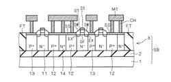
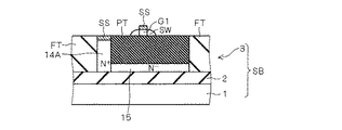
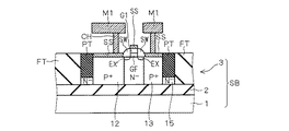
図1は半導体装置100の構成を示す平面図であり、図1に示すA−A線、B−B線、D−D線およびE−E線での矢示断面を、それぞれ図2、図3、図4および図5に示す。
FIG. 1 is a plan view showing the configuration of the
図1に示すように半導体装置100は、Pチャネル型MOSトランジスタ(PMOSトランジスタ)P1と、Nチャネル型MOSトランジスタ(NMOSトランジスタ)N1とを有し、両トランジスタのゲート電極G1は共通に接続されている。
As shown in FIG. 1, the
そして、PMOSトランジスタP1においては、ソース・ドレイン領域がゲート幅方向に沿って4分割され、4つの独立したソース領域12の配列と、4つの独立したドレイン領域13の配列とを有した構成となっている。
In the PMOS transistor P1, the source / drain region is divided into four along the gate width direction, and has an arrangement of four
4つのソース領域12の間には、対向する側面全体に接するように部分トレンチ分離絶縁膜PTが設けられ、また、配列の両端に位置するソース領域12の外側にも部分トレンチ分離絶縁膜PTが設けられている。当該部分トレンチ分離絶縁膜PT(第1の部分トレンチ分離絶縁膜)はゲート電極G1の下方に形成されるチャネル領域をチャネル長方向に横切って分割するように配設されている。なお、ソース領域、ドレイン領域、チャネル領域を分割する部分トレンチ分離絶縁膜は、分割用部分トレンチ分離絶縁膜と呼称する場合がある。
A partial trench isolation insulating film PT is provided between the four
そして、ソース領域12のゲート電極G1とは反対側の側面に接するようにN型不純物を比較的高濃度(N+)に含んだボディ固定領域14(第3の半導体領域)が設けられ、当該ボディ固定領域14は、4つのソース領域12の側面に接するとともに、部分トレンチ分離絶縁膜PTのゲート電極G1とは反対側の側面にも接して、ゲート電極G1と平行して延在するように配設されている。
A body fixing region 14 (third semiconductor region) containing an N-type impurity at a relatively high concentration (N + ) is provided so as to be in contact with the side surface of the
また、ゲート電極G1の下方に形成されるチャネル領域を横切った部分トレンチ分離絶縁膜PTはドレイン領域13に達し、4つのドレイン領域13の間にも部分トレンチ分離絶縁膜PTが設けられているが、ドレイン領域13の対向する側面全体に接するのではなく、ゲート電極G1から所定長さだけ部分トレンチ分離絶縁膜PTが突出するように設けられている。これは、配列の両端に位置するドレイン領域13の外側においても同様である。
Further, the partial trench isolation insulating film PT crossing the channel region formed below the gate electrode G1 reaches the
ここで、部分トレンチ分離絶縁膜PTが突出する長さは、部分トレンチ分離絶縁膜PTとゲート電極や半導体領域との重ね合わせ精度に基づいて設定される。このように部分トレンチ分離絶縁膜PTを突出させることで、確実にゲート電極下のボディ領域と接続されるという効果が得られる。 Here, the length by which the partial trench isolation insulating film PT protrudes is set based on the overlay accuracy of the partial trench isolation insulating film PT and the gate electrode or semiconductor region. By projecting the partial trench isolation insulating film PT in this way, an effect of reliably connecting to the body region under the gate electrode can be obtained.
なお、ソース領域およびドレイン領域の配列の両端に位置するソース領域およびドレイン領域の外側に配設される部分トレンチ分離絶縁膜は、外周部分トレンチ分離絶縁膜と呼称する場合がある。 The partial trench isolation insulating film disposed outside the source region and the drain region located at both ends of the arrangement of the source region and the drain region may be referred to as an outer peripheral partial trench isolation insulating film.
NMOSトランジスタN1においては、ソース・ドレイン領域がゲート幅方向に沿って2分割され、2つの独立したソース領域22の配列と、2つの独立したドレイン領域23の配列とを有した構成となっている。
In the NMOS transistor N1, the source / drain region is divided into two along the gate width direction, and has an arrangement of two
2つのソース領域22の間には、対向する側面全体に接するように部分トレンチ分離絶縁膜PTが設けられ、また、配列の両端に位置するソース領域22の外側にも部分トレンチ分離絶縁膜PTが設けられている。
A partial trench isolation insulating film PT is provided between the two
そして、ソース領域22のゲート電極G1とは反対側の側面に接するようにP型不純物を比較的高濃度(P+)に含んだボディ固定領域24(第3の半導体領域)が設けられ、当該ボディ固定領域24は、2つのソース領域22の側面に接するとともに、部分トレンチ分離絶縁膜PTのゲート電極G1とは反対側の側面にも接して、ゲート電極G1と平行して延在するように配設されている。
A body fixing region 24 (third semiconductor region) containing P-type impurities at a relatively high concentration (P + ) is provided so as to be in contact with the side surface of the
なお、ボディ固定領域14および24を、ゲート電極G1と平行して延在するように構成することで、ボディ固定領域14および24が、ソース領域の配列方向に多少ずれるように形成された場合でも、部分トレンチ分離絶縁膜PTとの接触が完全に断たれてしまうことがなく、MOSトランジスタの動作不良の発生を防止できる。
Even when the
また、2つのドレイン領域23の間にも部分トレンチ分離絶縁膜PTが設けられているが、ドレイン領域23の対向する側面全体に接するのではなく、ゲート電極G1から所定長さだけ部分トレンチ分離絶縁膜PTが突出するように設けられている。これは、配列の両端に位置するドレイン領域23の外側においても同様である。
A partial trench isolation insulating film PT is also provided between the two
ここで、部分トレンチ分離絶縁膜PTが突出する長さは、部分トレンチ分離絶縁膜PTとゲート電極や半導体領域との重ね合わせ精度に基づいて設定される。このように部分トレンチ分離絶縁膜PTを突出させることで、確実にゲート電極下のボディ領域と接続されるという効果が得られる。 Here, the length by which the partial trench isolation insulating film PT protrudes is set based on the overlay accuracy of the partial trench isolation insulating film PT and the gate electrode or semiconductor region. By projecting the partial trench isolation insulating film PT in this way, an effect of reliably connecting to the body region under the gate electrode can be obtained.
ここで、図2〜図5に示すように、半導体装置100は、シリコン基板1と、当該シリコン基板1上に配設された埋め込み酸化膜2と、埋め込み酸化膜2上に配設されたSOI層3とで構成されるSOI基板SB上に配設されている。そして、PMOSトランジスタP1およびNMOSトランジスタN1の周囲は完全トレンチ分離絶縁膜FTによって囲まれており、図3に示すように、PMOSトランジスタP1の活性層とNMOSトランジスタN1の活性層とは電気的に分離されている。
As shown in FIGS. 2 to 5, the
また、図2に示すように、PMOSトランジスタP1のボディ固定領域14は、SOI層3の表面から埋め込み酸化膜2に達するように設けられ、部分トレンチ分離絶縁膜PTの下層に存在するN型不純物を比較的低濃度(N-)に含んだウエル領域15と接触する構成となっている。なお、ボディ固定領域14の上面はシリサイド膜SSで覆われている。
As shown in FIG. 2, the
ウエル領域15は、図4に示すようにボディ領域11に連続しており、ウエル領域15を通じてボディ固定領域14とボディ領域11との間でキャリアの移動が可能な構成となっている。なお、この構成は、NMOSトランジスタN1のボディ固定領域24、部分トレンチ分離絶縁膜PTの下層に存在するP型不純物を比較的低濃度(P-)に含んだウエル領域25およびボディ領域21においても同様である。
As shown in FIG. 4, the
また、図5に示すように、PMOSトランジスタP1のボディ領域11の上方にゲート絶縁膜GFを介してゲート電極G1が設けられ、ゲート電極G1の側面にはサイドウォール絶縁膜SWが設けられている。
As shown in FIG. 5, a gate electrode G1 is provided above the
そして、ゲート電極G1のゲート長方向の両側面外方のボディ領域11の表面内には、エクステンション層EXが設けられ、エクステンション層EXはソース領域12およびドレイン領域13に接触している。
An extension layer EX is provided in the surface of the
エクステンション層は、ソース・ドレイン領域よりも浅い接合となるように形成される不純物層であり、ソース・ドレイン領域と同一導電型であり、ソース・ドレイン領域として機能するのでソース・ドレインエクステンション層と呼称すべきであるが、便宜的にエクステンション層と呼称する。ここで、エクステンション層EX間のボディ領域11内にゲート電極G1に沿ってチャネル領域が形成されるが、チャネル領域は図示していない。これはNMOSトランジスタN1においても同様である。
The extension layer is an impurity layer formed so as to have a shallower junction than the source / drain region, and has the same conductivity type as the source / drain region and functions as the source / drain region, so it is called a source / drain extension layer. It should be called an extension layer for convenience. Here, a channel region is formed along the gate electrode G1 in the
なお、図5に示すように、ソース領域12およびドレイン領域13は、SOI層3の表面から埋め込み酸化膜2に達するように設けられ、ソース領域12およびドレイン領域13の上面はシリサイド膜SSで覆われ、また、ゲート電極G1の上面もシリサイド膜SSで覆われている。
As shown in FIG. 5, the
NMOSトランジスタN1においても上記と同様のゲート構造を有し、ソース領域22およびドレイン領域23の上面はシリサイド膜SSで覆われている。なお、図1においては便宜的にシリサイド膜SSは省略している。
The NMOS transistor N1 also has the same gate structure as described above, and the upper surfaces of the
また、図1においては省略しているが、図4に示すようにゲート電極G1はコンタクトホールCHを介して上層の配線層M1に電気的に接続される。同様に、図5に示すように、ソース領域12、ドレイン領域13およびボディ固定領域14は、コンタクトホールCHを介して上層の配線層M1に接続される。なお、ソース領域12とボディ固定領域14とはシリサイド膜SSを介して電気的に接続されるが、図5に示されるように、ソース領域12とボディ固定領域14とを共通の配線層M1に接続しても良いことは言うまでもない。
Although omitted in FIG. 1, as shown in FIG. 4, the gate electrode G1 is electrically connected to the upper wiring layer M1 through the contact hole CH. Similarly, as shown in FIG. 5, the
ソース領域12とボディ固定領域14とを電気的に接続することで、PMOSトランジスタP1のボディ領域11がソース領域12の電位に固定されることになる。
By electrically connecting the
また、NMOSトランジスタN1においては、ボディ領域21がソース領域22の電位に固定されることになる。
In the NMOS transistor N1, the
<A−2.効果>
以上説明したように、半導体装置100においては、PMOSトランジスタP1ではソース・ドレイン領域をゲート幅方向に沿って4分割することで、実質的にPMOSトランジスタP1側のゲート電極G1を4分割し、分割されたゲート電極のそれぞれについて、ボディ固定領域14からウエル領域15を通じてボディ領域11の電位を固定する。また、NMOSトランジスタN1ではソース・ドレイン領域をゲート幅方向に沿って2分割することで、実質的にNMOSトランジスタN1側のゲート電極G1を2分割し、分割されたゲート電極のそれぞれについて、ボディ固定領域24からウエル領域25を通じてボディ領域21の電位を固定する。
<A-2. Effect>
As described above, in the
従って、PMOSトランジスタP1およびNMOSトランジスタN1においては、ボディ領域11および21の電位固定を確実に行うことができ、キンクの発生を抑制することができる。
Therefore, in the PMOS transistor P1 and the NMOS transistor N1, the potentials of the
また、PMOSトランジスタP1およびNMOSトランジスタN1においては、実質的にゲート電極G1を分割するので、動作耐圧を向上させることができる。 In addition, since the gate electrode G1 is substantially divided in the PMOS transistor P1 and the NMOS transistor N1, the operating breakdown voltage can be improved.
すなわち、MOSトランジスタの動作耐圧はチャネル幅によって制限され、チャネル幅が長くなると、動作耐圧が低下する。 That is, the operating breakdown voltage of the MOS transistor is limited by the channel width, and the operating breakdown voltage decreases as the channel width increases.
これは、駆動能力の大きなNMOSトランジスタの方が顕著であり、PMOSトランジスタは、NMOSトランジスタよりもチャネル幅を長くできる。 This is more remarkable in the NMOS transistor having a large driving capability, and the PMOS transistor can have a longer channel width than the NMOS transistor.
しかし、何れにせよ動作耐圧はチャネル幅によって制限されるが、部分トレンチ分離絶縁膜PTによってゲート電極G1下のチャネル領域をゲート幅方向に分割することで、チャネル幅が実質的に短くなり、1つのチャネル領域に印加可能な電圧を高くでき、トランジスタ全体の動作耐圧を向上させることができる。 However, in any case, the operating breakdown voltage is limited by the channel width, but by dividing the channel region under the gate electrode G1 by the partial trench isolation insulating film PT in the gate width direction, the channel width is substantially shortened. The voltage that can be applied to one channel region can be increased, and the operating breakdown voltage of the entire transistor can be improved.
また、ソース・ドレイン領域を部分トレンチ分離絶縁膜PTおよび完全トレンチ分離絶縁膜FTによって分割することで、実質的にゲート電極G1をゲート幅方向に分割するが、トレンチ分離絶縁膜を形成する際には加工精度の高いマスクを使用するので、ゲート電極G1を設計値に従って精度良く分割することができ、ゲート幅にばらつきが生じることを防止して、動作特性にばらつきを生じない半導体装置を得ることができる。 Further, the source / drain region is divided by the partial trench isolation insulating film PT and the complete trench isolation insulating film FT to substantially divide the gate electrode G1 in the gate width direction, but when forming the trench isolation insulating film Uses a mask with high processing accuracy, so that the gate electrode G1 can be divided with high accuracy according to the design value, and it is possible to prevent the gate width from varying and to obtain a semiconductor device that does not vary in operating characteristics. Can do.
また、PMOSトランジスタP1のドレイン領域13およびNMOSトランジスタN1のドレイン領域23の側面は、大部分が完全トレンチ分離絶縁膜FTに接しており、部分トレンチ分離絶縁膜PTに接する部分は一部分だけである。
Further, most of the side surfaces of the
このような構成を採ることで、ドレイン領域13および23の大部分が完全トレンチ分離絶縁膜FTで囲まれ、その分だけ、PN接合の接合面積が減るので、ドレイン領域13および23における寄生接合容量が小さく、充放電に費やす時間が少なくて済むので、MOSトランジスタの動作速度が低下することを防止できる。
By adopting such a configuration, most of the
一方、PMOSトランジスタP1のソース領域12の側面は、部分トレンチ分離絶縁膜PTおよびボディ固定領域14に接し、また、NMOSトランジスタN1のソース領域22の側面は、部分トレンチ分離絶縁膜PTおよびボディ固定領域24に接するので、ソース領域12および22におけるPN接合の接合面積が広くなり、寄生接合容量が大きくなるが、ソース領域側における接合容量の増加は電流の安定供給に寄与するので、電源供給を安定化させることができる。
On the other hand, the side surface of the
また、半導体装置100の上方には配線層M1が配設されるが、完全トレンチ分離絶縁膜FT上の配線層M1に寄生する寄生容量と、部分トレンチ分離絶縁膜PT上の配線層M1に寄生する寄生容量とでは、後者の方が大きくなる。
Further, although the wiring layer M1 is disposed above the
従って、ドレイン領域13および23側では部分トレンチ分離絶縁膜PTの形成領域を最小限に止めることで、配線層M1に寄生する寄生容量を抑制して、MOSトランジスタの動作速度が低下することを防止できる。
Therefore, by minimizing the formation region of the partial trench isolation insulating film PT on the
<A−3.応用例>
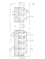
以上説明した半導体装置100は、ゲート電極G1が共通に接続されたPMOSトランジスタP1およびNMOSトランジスタN1の配列を示したが、図6においては、ゲート電極G1が共通に接続されたPMOSトランジスタP11およびNMOSトランジスタN11の配列(第1の組)、PMOSトランジスタP12およびNMOSトランジスタN12の配列(第2の組)、PMOSトランジスタP13およびNMOSトランジスタN13の配列(第3の組)の3組のトランジスタの配列を配設した半導体装置100Aの構成を示す。
<A-3. Application example>
The
なお、図6に示す半導体装置100Aにおいて、図1に示した半導体装置100と同一の構成については同一の符号を付し、重複する説明は省略する。また、図6に示すF−F線およびG−G線での矢示断面を、それぞれ図7および図8に示す。なお、B−B線およびD−D線での断面構成は、それぞれ図3および図4に示した構成と同じである。
Note that in the
図6に示すように、第1の組と第2の組においてはドレイン領域13および23を共通に使用しており、第2の組と第3の組においては、ボディ固定領域14および24を共通に使用している。
As shown in FIG. 6, the
また、図7に示すように、PMOSトランジスタP11およびP12のドレイン領域13間は、完全トレンチ分離絶縁膜FTによって電気的に分離されている。従って、ドレイン領域13どうしを電気的に接続するには、図8に示すように各ドレイン領域13をコンタクトホールCHを介して上層の配線層M1に共通に接続することになる。
As shown in FIG. 7, the
このような構成を採ることで、第1の組〜第3の組において、PMOSトランジスタP11〜P13が並列に接続され、NMOSトランジスタN11〜N13が並列に接続された構成を、極力小さなレイアウト面積で得ることができる。 By adopting such a configuration, in the first to third groups, the PMOS transistors P11 to P13 are connected in parallel and the NMOS transistors N11 to N13 are connected in parallel with a layout area as small as possible. Obtainable.
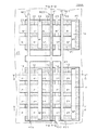
ここで、半導体装置100Aの上層に配設される配線層M1の配設パターンの一例を図9に示す。
Here, FIG. 9 shows an example of the arrangement pattern of the wiring layer M1 arranged on the upper layer of the
図9に示すように、PMOSトランジスタP11〜P13の複数のドレイン領域13およびNMOSトランジスタN11〜N13の複数のドレイン領域23は、それぞれコンタクトホールCHを介して配線層M1に接続され、当該配線層M1は出力端子OUTに接続されている。
As shown in FIG. 9, the plurality of
また、PMOSトランジスタP11〜P13の複数のソース領域12およびボディ固定領域14は、それぞれコンタクトホールCHを介して配線層M1に接続され、当該配線層M1は電源電位VDDに接続され、NMOSトランジスタN11〜N13の複数のソース領域22およびボディ固定領域24は、それぞれコンタクトホールCHを介して配線層M1に接続され、当該配線層M1は接地電位GNDに接続されている。
The plurality of
また、複数のゲート電極G1は共通して配線層M1に接続され、当該配線層M1は入力端子INに接続されている。 The plurality of gate electrodes G1 are commonly connected to the wiring layer M1, and the wiring layer M1 is connected to the input terminal IN.
このような配線を行うことで、半導体装置100Aはインバータとして機能する。なお、図9においては、上記インバータを回路記号で表したものを併記している。
By performing such wiring, the
また、図10には、半導体装置100Aの上層に配設される配線層M1の配設パターンの他の例を示す。
FIG. 10 shows another example of the arrangement pattern of the wiring layer M1 arranged on the upper layer of the
図10においては、基本的には図9に示した配線層M1の配設パターンと同じであり、半導体装置100Aをインバータとして使用する配線を示しているが、PMOSトランジスタP11〜P13の複数のソース領域12およびNMOSトランジスタN11〜N13の複数のソース領域22のうち、それぞれ一部だけがコンタクトホールCHを介して配線層M1に接続され、残りのソース領域12および22は配線層M1には接続されていない。
FIG. 10 is basically the same as the arrangement pattern of the wiring layer M1 shown in FIG. 9 and shows wiring using the
各トランジスタにおける全てのソース領域12および22は、図8に示すようにシリサイド膜SSで共通に覆われており、電気的に接続されているので、その一部を配線層M1に電気的に接続すれば、各トランジスタのソース領域は共通して配線層M1に電気的に接続されることになる。
All the
<B.実施の形態2>
<B−1.装置構成>
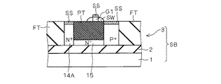
図11〜図15を用いて本発明に係る実施の形態2の半導体装置200の構成について説明する。
<B. Second Embodiment>
<B-1. Device configuration>
The configuration of the
図11は半導体装置200の構成を示す平面図であり、図11に示すA−A線、B−B線、D−D線およびE−E線での矢示断面を、それぞれ図12、図13、図14および図15に示す。なお、図1〜5に示した半導体装置100と同一の構成については同一の符号を付し、重複する説明は省略する。
FIG. 11 is a plan view showing the configuration of the
図11に示すように半導体装置200においては、PMOSトランジスタP2のソース領域12のゲート電極G1とは反対側の側面に接するようにN型不純物を比較的高濃度(N+)に含んだボディ固定領域14が設けられ、当該ボディ固定領域14は、4つのソース領域12の側面に接するとともに、部分トレンチ分離絶縁膜PTのゲート電極G1とは反対側の側面にも接して、ゲート電極G1と平行して延在するように配設されている。
As shown in FIG. 11, in the
4つのソース領域12の間には、対向する側面全体に接するように部分トレンチ分離絶縁膜PTが設けられ、また、配列の両端に位置するソース領域12の外側にも、部分トレンチ分離絶縁膜PTが設けられ、当該部分トレンチ分離絶縁膜PTは、ボディ固定領域14の長手方向端部の側面にも接するように配設されている。
A partial trench isolation insulating film PT is provided between the four
そして、ボディ固定領域14のゲート電極G1とは反対側の側面に接するように(図12参照)部分トレンチ分離絶縁膜PT(第2の部分トレンチ分離絶縁膜)が設けられ、ボディ固定領域14は部分トレンチ分離絶縁膜PTによって囲まれている。なお、ボディ固定領域の側面に接するように配設される部分トレンチ分離絶縁膜は、外周部分トレンチ分離絶縁膜と呼称する場合がある。
A partial trench isolation insulating film PT (second partial trench isolation insulating film) is provided so as to be in contact with the side surface of the
また、PMOSトランジスタ領域においては、部分トレンチ分離絶縁膜PTの下層にはN型不純物を比較的低濃度(N-)に含んだウエル領域15が存在し、図12および図15に示されるように、ボディ固定領域14とウエル領域15とが接触する構成となっている。
In the PMOS transistor region, a
NMOSトランジスタN2においては、ソース領域22のゲート電極G1とは反対側の側面に接するようにP型不純物を比較的高濃度(P+)に含んだボディ固定領域24が設けられ、当該ボディ固定領域24は、2つのソース領域22の側面に接するとともに、部分トレンチ分離絶縁膜PTのゲート電極G1とは反対側の側面にも接して、ゲート電極G1と平行して延在するように配設されている。
In the NMOS transistor N2, a
2つのソース領域22の間には、対向する側面全体に接するように部分トレンチ分離絶縁膜PTが設けられ、また、配列の両端に位置するソース領域22の外側にも部分トレンチ分離絶縁膜PTが設けられ、当該部分トレンチ分離絶縁膜PTは、ボディ固定領域24の長手方向端部の側面にも接するように配設されている。
A partial trench isolation insulating film PT is provided between the two
そして、ボディ固定領域24のゲート電極G1とは反対側の側面に接するように部分トレンチ分離絶縁膜PTが設けられ、ボディ固定領域24は部分トレンチ分離絶縁膜PTによって囲まれている。なお、NMOSトランジスタ領域においては、部分トレンチ分離絶縁膜PTの下層にはP型不純物を比較的低濃度(P-)に含んだウエル領域25が存在しており、図示はしていないが、ボディ固定領域24とウエル領域25とが接触する構成となっている。
A partial trench isolation insulating film PT is provided so as to contact the side surface of the
その他の構成については、図1〜5に示した半導体装置100と同一であり説明は省略する。
Other configurations are the same as those of the
<B−2.効果>
以上説明した半導体装置200においては、MOSトランジスタのソース・ドレイン領域をゲート幅方向に沿って分割することで、図1〜図5を用いて説明した半導体装置100と同様に、PMOSトランジスタP2およびNMOSトランジスタN2においては、ボディ領域11および21の電位固定を確実に行うことができ、キンクの発生を抑制できるとともに、動作耐圧を向上させることができる。
<B-2. Effect>
In the
また、ソース・ドレイン領域を部分トレンチ分離絶縁膜PTおよび完全トレンチ分離絶縁膜FTによって分割することで、実質的にゲート電極G1をゲート幅方向に分割するが、トレンチ分離絶縁膜を形成する際には加工精度の高いマスクを使用するので、ゲート電極G1を設計値に従って精度良く分割することができ、ゲート幅にばらつきが生じることを防止して、動作特性にばらつきを生じない半導体装置を得ることができる。 Further, the source / drain region is divided by the partial trench isolation insulating film PT and the complete trench isolation insulating film FT to substantially divide the gate electrode G1 in the gate width direction, but when forming the trench isolation insulating film Uses a mask with high processing accuracy, so that the gate electrode G1 can be divided with high accuracy according to the design value, and it is possible to prevent the gate width from varying and to obtain a semiconductor device that does not vary in operating characteristics. Can do.
また、ドレイン領域13および23の大部分が完全トレンチ分離絶縁膜FTで囲まれた構成を採ることで、その分だけ、PN接合の接合面積が減るので、ドレイン領域13および23における寄生接合容量が小さく、MOSトランジスタの動作速度が低下することを防止できる。
Further, by adopting a configuration in which most of the
一方、PMOSトランジスタP2のソース領域12の側面は、部分トレンチ分離絶縁膜PTおよびボディ固定領域14に接し、また、NMOSトランジスタN2のソース領域22の側面は、部分トレンチ分離絶縁膜PTおよびボディ固定領域24に接するので、ソース領域12および22におけるPN接合の接合面積が広くなり、寄生接合容量が大きくなり、電源供給を安定化させることができる。
On the other hand, the side surface of the
さらに、ボディ固定領域14のゲート電極G1とは反対側の側面に接するように部分トレンチ分離絶縁膜PTが設けられ、ボディ固定領域14は部分トレンチ分離絶縁膜PTによって囲まれているので、部分トレンチ分離絶縁膜PT上に配線層M1を配設した場合に、当該配線層M1に寄生する寄生容量をさらに増やすことができ、電源供給を安定化させることができる。
Further, the partial trench isolation insulating film PT is provided so as to be in contact with the side surface of the
なお、ドレイン領域13および23側では部分トレンチ分離絶縁膜PTの形成領域を最小限に止めることで、配線層M1に寄生する寄生容量を抑制して、MOSトランジスタの動作速度が低下することを防止できる。
In addition, by suppressing the formation region of the partial trench isolation insulating film PT to the minimum on the
<B−3.応用例>
以上説明した半導体装置200は、ゲート電極G1が共通に接続されたPMOSトランジスタP2およびNMOSトランジスタN2の配列を示したが、図16においては、ゲート電極G1が共通に接続されたPMOSトランジスタP21およびNMOSトランジスタN21の配列(第1の組)、PMOSトランジスタP22およびNMOSトランジスタN22の配列(第2の組)、PMOSトランジスタP23およびNMOSトランジスタN23の配列(第3の組)の3組のトランジスタの配列を配設した半導体装置200Aの構成を示す。
<B-3. Application example>
The
なお、図16に示す半導体装置200Aにおいては、図6に示した半導体装置100Aと同一の構成については同一の符号を付し、重複する説明は省略する。また、図16に示すF−F線およびG−G線での矢示断面を、それぞれ図17および図18に示す。なお、B−B線およびD−D線での断面構成は、それぞれ図13および図14に示した構成と同じである。
Note that in the
図16に示すように、第1の組と第2の組においてはドレイン領域13および23を共通に使用しており、第2の組と第3の組においては、ボディ固定領域14および24を共通に使用している。
As shown in FIG. 16, the
また、図17に示すように、PMOSトランジスタP21およびP22のドレイン領域13間は、完全トレンチ分離絶縁膜FTによって電気的に分離されている。従って、ドレイン領域13どうしを電気的に接続するには、図18に示すように各ドレイン領域13をコンタクトホールCHを介して上層の配線層M1に共通に接続することになる。これは、NMOSトランジスタN21およびN22のドレイン領域23間においても同じである。
As shown in FIG. 17, the
このような構成を採ることで、第1の組〜第3の組において、PMOSトランジスタP21〜P23が並列に接続され、NMOSトランジスタN21〜N23が並列に接続された構成を、極力小さなレイアウト面積で得ることができる。 By adopting such a configuration, in the first to third sets, the PMOS transistors P21 to P23 are connected in parallel and the NMOS transistors N21 to N23 are connected in parallel with a layout area as small as possible. Obtainable.
ここで、半導体装置100Aの上層に配設される配線層M1の配設パターンの一例を図19に示す。
Here, FIG. 19 shows an example of an arrangement pattern of the wiring layer M1 arranged on the upper layer of the
図19に示すように、PMOSトランジスタP21〜P23の複数のドレイン領域13およびNMOSトランジスタN21〜N23の複数のドレイン領域23は、それぞれコンタクトホールCHを介して配線層M1に接続され、当該配線層M1は出力端子OUTに接続されている。
As shown in FIG. 19, the plurality of
また、PMOSトランジスタP21〜P23の複数のソース領域12およびボディ固定領域14は、それぞれコンタクトホールCHを介して配線層M1に接続され、当該配線層M1は電源電位VDDに接続され、NMOSトランジスタN21〜N23の複数のソース領域22およびボディ固定領域24は、それぞれコンタクトホールCHを介して配線層M1に接続され、当該配線層M1は接地電位GNDに接続されている。
The plurality of
また、複数のゲート電極G1は共通して配線層M1に接続され、当該配線層M1は入力端子INに接続されている。 The plurality of gate electrodes G1 are commonly connected to the wiring layer M1, and the wiring layer M1 is connected to the input terminal IN.
このような配線を行うことで、半導体装置200Aはインバータとして機能する。なお、図19においては、上記インバータを回路記号で表したものを併記している。
By performing such wiring, the
また、図20には、半導体装置200Aの上層に配設される配線層M1の配設パターンの他の例を示す。
FIG. 20 shows another example of the arrangement pattern of the wiring layer M1 arranged on the upper layer of the
図20においては、基本的には図19に示した配線層M1の配設パターンと同じであり、半導体装置100Aをインバータとして使用する配線を示しているが、PMOSトランジスタP21〜P23の複数のソース領域12およびNMOSトランジスタN21〜N23の複数のソース領域22のうち、それぞれ一部だけがコンタクトホールCHを介して配線層M1に接続され、残りのソース領域12および22は配線層M1には接続されていない。
20 is basically the same as the arrangement pattern of the wiring layer M1 shown in FIG. 19 and shows wiring using the
各トランジスタにおける全てのソース領域12および22は、図18に示すようにシリサイド膜SSで共通に覆われており、電気的に接続されているので、その一部を配線層M1に電気的に接続すれば、各トランジスタのソース領域は共通して配線層M1に電気的に接続されることになる。
All the
<C.実施の形態3>
<C−1.装置構成>
図21〜図25を用いて本発明に係る実施の形態3の半導体装置300の構成について説明する。
<
<C-1. Device configuration>
The configuration of the
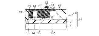
図21は半導体装置300の構成を示す平面図であり、図21に示すA−A線、B−B線、D−D線およびE−E線での矢示断面を、それぞれ図22、図23、図24および図25に示す。なお、図1〜5に示した半導体装置100と同一の構成については同一の符号を付し、重複する説明は省略する。
21 is a plan view showing the configuration of the
図21に示すように半導体装置300のPMOSトランジスタP3においては、ソース領域がゲート幅方向に沿って4分割され、4つの独立したソース領域12の配列を有した構成となっている。
As shown in FIG. 21, in the PMOS transistor P3 of the
すなわち、4つのソース領域12の間には、対向する側面全体に接するように部分トレンチ分離絶縁膜PTが設けられ、また、配列の両端に位置するソース領域12の外側にも部分トレンチ分離絶縁膜PTが設けられている。
That is, a partial trench isolation insulating film PT is provided between the four
一方、ドレイン領域13Aにおいては、ゲート電極G1から所定長さだけ部分トレンチ分離絶縁膜PTが突出するように設けられているが、ゲート電極G1とは反対側の部分が連続した構成となっており、分割されてはおらず、ドレイン領域13Aが突出した部分トレンチ分離絶縁膜PTを囲むように構成されている。
On the other hand, in the
NMOSトランジスタN3においては、ソース領域がゲート幅方向に沿って2分割され、2つの独立したソース領域22の配列を有した構成となっている。
The NMOS transistor N3 has a configuration in which the source region is divided into two along the gate width direction and has an array of two
すなわち、2つのソース領域22の間には、対向する側面全体に接するように部分トレンチ分離絶縁膜PTが設けられ、また、配列の両端に位置するソース領域22の外側にも部分トレンチ分離絶縁膜PTが設けられている。
That is, a partial trench isolation insulating film PT is provided between the two
一方、ドレイン領域23Aにおいては、ゲート電極G1から所定長さだけ部分トレンチ分離絶縁膜PTが突出するように設けられているが、ゲート電極G1とは反対側の部分が連続した構成となっており、分割されてはおらず、ドレイン領域23Aが突出した部分トレンチ分離絶縁膜PTを囲むように構成されている。
On the other hand, in the
その他の構成については、図1〜5に示した半導体装置100と同一であり説明は省略する。
Other configurations are the same as those of the
<C−2.効果>
以上説明した半導体装置300においては、MOSトランジスタのソース領域をゲート幅方向に沿って分割することで、図1〜図5を用いて説明した半導体装置100と同様に、PMOSトランジスタP3およびNMOSトランジスタN3においては、ボディ領域11および21の電位固定を確実に行うことができ、キンクの発生を抑制するとともに、動作耐圧を向上させることができる。
<C-2. Effect>
In the
また、ソース領域12および22を部分トレンチ分離絶縁膜PTによって分割することで、実質的にゲート電極G1をゲート幅方向に分割するが、トレンチ分離絶縁膜を形成する際には加工精度の高いマスクを使用するので、ゲート電極G1を設計値に従って精度良く分割することができ、ゲート幅にばらつきが生じることを防止して、動作特性にばらつきを生じない半導体装置を得ることができる。
The
なお、ドレイン領域13Aおよび23Aは連続した構成となっているので、少なくとも1カ所に電位固定のためのコンタクトホールを接続すれば良く、コンタクトホールを形成する工程を簡略化できる。
Since the
また、ドレイン領域13Aおよび23Aの大部分が完全トレンチ分離絶縁膜FTで囲まれた構成を採ることで、その分だけ、PN接合の接合面積が減るので、ドレイン領域13Aおよび23Aにおける寄生接合容量が小さく、MOSトランジスタの動作速度が低下することを防止できる。
Further, by adopting a configuration in which most of the
一方、PMOSトランジスタP3のソース領域12の側面は、部分トレンチ分離絶縁膜PTおよびボディ固定領域14に接し、また、NMOSトランジスタN3のソース領域22の側面は、部分トレンチ分離絶縁膜PTおよびボディ固定領域24に接するので、ソース領域12および22におけるPN接合の接合面積が広くなり、寄生接合容量が大きくなり、電源供給を安定化させることができる。
On the other hand, the side surface of the
なお、ドレイン領域13Aおよび23A側では部分トレンチ分離絶縁膜PTの形成領域を最小限に止めることで、配線層M1に寄生する寄生容量を抑制して、MOSトランジスタの動作速度が低下することを防止できる。
In addition, by suppressing the formation region of the partial trench isolation insulating film PT to the minimum on the
<D.実施の形態4>
<D−1.装置構成>
図26〜図30を用いて本発明に係る実施の形態4の半導体装置400の構成について説明する。
<
<D-1. Device configuration>
The configuration of the
図26は半導体装置400の構成を示す平面図であり、図26に示すA−A線、B−B線、D−D線およびE−E線での矢示断面を、それぞれ図27、図28、図29および図30に示す。なお、図1〜5に示した半導体装置100と同一の構成については同一の符号を付し、重複する説明は省略する。
26 is a plan view showing the configuration of the
図26に示すように半導体装置400においては、PMOSトランジスタP4のソース領域12のゲート電極G1とは反対側の側面に接するようにN型不純物を比較的高濃度(N+)に含んだボディ固定領域14が設けられ、当該ボディ固定領域14は、4つのソース領域12の側面に接するとともに、部分トレンチ分離絶縁膜PTのゲート電極G1とは反対側の側面にも接して、ゲート電極G1と平行して延在するように配設されている。
As shown in FIG. 26, in the
4つのソース領域12の間には、対向する側面全体に接するように部分トレンチ分離絶縁膜PTが設けられ、また、配列の両端に位置するソース領域12の外側にも、部分トレンチ分離絶縁膜PTが設けられ、当該部分トレンチ分離絶縁膜PTは、ボディ固定領域14の長手方向端部の側面にも接するように配設されている。
A partial trench isolation insulating film PT is provided between the four
そして、ボディ固定領域14のゲート電極G1とは反対側の側面に接するように(図27参照)部分トレンチ分離絶縁膜PTが設けられ、ボディ固定領域14は部分トレンチ分離絶縁膜PTによって囲まれている。なお、PMOSトランジスタ領域においては、部分トレンチ分離絶縁膜PTの下層にはN型不純物を比較的低濃度(N-)に含んだウエル領域15が存在し、図27および図30に示されるように、ボディ固定領域14とウエル領域15とが接触する構成となっている。
A partial trench isolation insulating film PT is provided so as to contact the side surface of the
NMOSトランジスタN4においては、ソース領域22のゲート電極G1とは反対側の側面に接するようにP型不純物を比較的高濃度(P+)に含んだボディ固定領域24が設けられ、当該ボディ固定領域24は、2つのソース領域22の側面に接するとともに、部分トレンチ分離絶縁膜PTのゲート電極G1とは反対側の側面にも接して、ゲート電極G1と平行して延在するように配設されている。
In the NMOS transistor N4, a
2つのソース領域22の間には、対向する側面全体に接するように部分トレンチ分離絶縁膜PTが設けられ、また、配列の両端に位置するソース領域22の外側にも部分トレンチ分離絶縁膜PTが設けられ、当該部分トレンチ分離絶縁膜PTは、ボディ固定領域24の長手方向端部の側面にも接するように配設されている。
A partial trench isolation insulating film PT is provided between the two
そして、ボディ固定領域24のゲート電極G1とは反対側の側面に接するように部分トレンチ分離絶縁膜PTが設けられ、ボディ固定領域24は部分トレンチ分離絶縁膜PTによって囲まれている。なお、NMOSトランジスタ領域においては、部分トレンチ分離絶縁膜PTの下層にはP型不純物を比較的低濃度(P-)に含んだウエル領域25が存在しており、図示はしていないが、ボディ固定領域24とウエル領域25とが接触する構成となっている。
A partial trench isolation insulating film PT is provided so as to contact the side surface of the
図26に示すように半導体装置400のPMOSトランジスタP4においては、ソース領域がゲート幅方向に沿って4分割され、4つの独立したソース領域12の配列を有した構成となっている。
As shown in FIG. 26, in the PMOS transistor P4 of the
一方、ドレイン領域13Aにおいては、ゲート電極G1から所定長さだけ部分トレンチ分離絶縁膜PTが突出するように設けられているが、ゲート電極G1とは反対側の部分が連続した構成となっており、分割されてはいない。
On the other hand, in the
NMOSトランジスタN4においては、ソース領域がゲート幅方向に沿って2分割され、2つの独立したソース領域22の配列を有した構成となっている。
The NMOS transistor N4 has a configuration in which the source region is divided into two along the gate width direction and has an array of two
一方、ドレイン領域23Aにおいては、ゲート電極G1から所定長さだけ部分トレンチ分離絶縁膜PTが突出するように設けられているが、ゲート電極G1とは反対側の部分が連続した構成となっており、分割されてはいない。
On the other hand, in the
その他の構成については、図1〜5に示した半導体装置100と同一であり説明は省略する。
Other configurations are the same as those of the
<D−2.効果>
以上説明した半導体装置400においては、図1〜図5を用いて説明した半導体装置100と同様に、MOSトランジスタのソース領域をゲート幅方向に沿って分割することで、PMOSトランジスタP4およびNMOSトランジスタN4においては、ボディ領域11および21の電位固定を確実に行うことができ、キンクの発生を抑制するとともに、動作耐圧を向上させることができる。
<D-2. Effect>
In the
また、ソース領域12および22を部分トレンチ分離絶縁膜PTによって分割することで、実質的にゲート電極G1をゲート幅方向に分割するが、トレンチ分離絶縁膜を形成する際には加工精度の高いマスクを使用するので、ゲート電極G1を設計値に従って精度良く分割することができ、ゲート幅にばらつきが生じることを防止して、動作特性にばらつきを生じない半導体装置を得ることができる。
The
また、ドレイン領域13Aおよび23Aの大部分が完全トレンチ分離絶縁膜FTで囲まれた構成を採ることで、その分だけ、PN接合の接合面積が減るので、ドレイン領域13Aおよび23Aにおける寄生接合容量が小さく、MOSトランジスタの動作速度が低下することを防止できる。
Further, by adopting a configuration in which most of the
一方、PMOSトランジスタP4のソース領域12の側面は、部分トレンチ分離絶縁膜PTおよびボディ固定領域14に接し、また、NMOSトランジスタN4のソース領域22の側面は、部分トレンチ分離絶縁膜PTおよびボディ固定領域24に接するので、ソース領域12および22におけるPN接合の接合面積が広くなり、寄生接合容量が大きくなり、電源供給を安定化させることができる。
On the other hand, the side surface of the
さらに、ボディ固定領域14のゲート電極G1とは反対側の側面に接するように部分トレンチ分離絶縁膜PTが設けられ、ボディ固定領域14は部分トレンチ分離絶縁膜PTによって囲まれているので、部分トレンチ分離絶縁膜PT上に配線層M1を配設した場合に、当該配線層M1に寄生する寄生容量をさらに増やすことができ、電源供給を安定化させることができる。
Further, the partial trench isolation insulating film PT is provided so as to be in contact with the side surface of the
なお、ドレイン領域13Aおよび23A側では部分トレンチ分離絶縁膜PTの形成領域を最小限に止めることで、配線層M1に寄生する寄生容量を抑制して、MOSトランジスタの動作速度が低下することを防止できる。
In addition, by suppressing the formation region of the partial trench isolation insulating film PT to the minimum on the
<D−3.応用例1>
以上説明した半導体装置400は、ゲート電極G1が共通に接続されたPMOSトランジスタP4およびNMOSトランジスタN4の配列を示したが、図31においては、応用例1として、ゲート電極G1が共通に接続されたPMOSトランジスタP41およびNMOSトランジスタN41の配列(第1の組)、PMOSトランジスタP42およびNMOSトランジスタN42の配列(第2の組)、PMOSトランジスタP43およびNMOSトランジスタN43の配列(第3の組)の3組のトランジスタの配列を配設した半導体装置400Aの構成を示す。
<D-3. Application Example 1>
In the
なお、図31に示す半導体装置400Aにおいては、図6に示した半導体装置100Aと同一の構成については同一の符号を付し、重複する説明は省略する。また、図31に示すF−F線およびG−G線での矢示断面を、それぞれ図32および図33に示す。なお、B−B線およびD−D線での断面構成は、それぞれ図13および図14に示した構成と同じである。
Note that in the
図31に示すように、第1の組と第2の組においてはドレイン領域13Aおよび23Aを共通に使用しており、第2の組と第3の組においては、ボディ固定領域14および24を共通に使用している。
As shown in FIG. 31, the
また、図31に示すように、PMOSトランジスタP41およびP42においてはドレイン領域13Aを共通に使用し、図32および図33に示すように、ドレイン領域13A上はシリサイド膜33によって覆われている。これは、NMOSトランジスタN41およびN42におけるドレイン領域23Aにおいても同じである。
As shown in FIG. 31, the
このような構成を採ることで、第1の組〜第3の組において、PMOSトランジスタP41〜P43が並列に接続され、NMOSトランジスタN41〜N43が並列に接続された構成を、極力小さなレイアウト面積で得ることができる。 By adopting such a configuration, in the first to third groups, the PMOS transistors P41 to P43 are connected in parallel and the NMOS transistors N41 to N43 are connected in parallel with a layout area as small as possible. Obtainable.
ここで、半導体装置400Aの上層に配設される配線層M1の配設パターンの一例を図34に示す。
Here, FIG. 34 shows an example of an arrangement pattern of the wiring layer M1 provided in the upper layer of the
図34に示すように、PMOSトランジスタP41〜P43のドレイン領域13AおよびNMOSトランジスタN41〜N43のドレイン領域23Aは、それぞれコンタクトホールCHを介して配線層M1に接続され、当該配線層M1は出力端子OUTに接続されている。
As shown in FIG. 34, the
また、PMOSトランジスタP41〜P43の複数のソース領域12およびボディ固定領域14は、それぞれコンタクトホールCHを介して配線層M1に接続され、当該配線層M1は電源電位VDDに接続され、NMOSトランジスタN41〜N43の複数のソース領域22およびボディ固定領域24は、それぞれコンタクトホールCHを介して配線層M1に接続され、当該配線層M1は接地電位GNDに接続されている。
The plurality of
また、複数のゲート電極G1は共通して配線層M1に接続され、当該配線層M1は入力端子INに接続されている。 The plurality of gate electrodes G1 are commonly connected to the wiring layer M1, and the wiring layer M1 is connected to the input terminal IN.
このような配線を行うことで、半導体装置400Aはインバータとして機能する。なお、図34においては、上記インバータを回路記号で表したものを併記している。
By performing such wiring, the
また、図35には、半導体装置400Aの上層に配設される配線層M1の配設パターンの他の例を示す。
FIG. 35 shows another example of the arrangement pattern of the wiring layer M1 arranged on the upper layer of the
図35においては、基本的には図34に示した配線層M1の配設パターンと同じであり、半導体装置400Aをインバータとして使用する配線を示しているが、PMOSトランジスタP41〜P43の複数のソース領域12およびNMOSトランジスタN41〜N43の複数のソース領域22のうち、それぞれ一部だけがコンタクトホールCHを介して配線層M1に接続され、残りのソース領域12および22は配線層M1には接続されていない。
In FIG. 35, the wiring pattern M1 is basically the same as the arrangement pattern of the wiring layer M1 shown in FIG. 34, and the wiring using the
各トランジスタにおける全てのソース領域12および22は、図33に示すようにシリサイド膜SSで共通に覆われており、電気的に接続されているので、その一部を配線層M1に電気的に接続すれば、各トランジスタのソース領域は共通して配線層M1に電気的に接続されることになる。
Since all the
また、図36には、半導体装置400Aの上層に配設される配線層M1の配設パターンのさらなる他の例を示す。
FIG. 36 shows still another example of the arrangement pattern of the wiring layer M1 arranged on the upper layer of the
図36においては、基本的には図35に示した配線層M1の配設パターンと同じであるが、PMOSトランジスタP41〜P43のドレイン領域13AおよびNMOSトランジスタN41〜N43のドレイン領域23Aにおいては、その上方の一部を覆うように配線層M1が形成され、配線層M1直下のドレイン領域13Aおよび23AがコンタクトホールCHを介して配線層M1に接続され、ドレイン領域13Aおよび23Aの他の部分は配線層M1には接続されていない。
36 is basically the same as the arrangement pattern of the wiring layer M1 shown in FIG. 35. However, in the
各トランジスタにおけるドレイン領域13Aおよび23A分割されておらず、また、図33に示すようにシリサイド膜SSで覆われているので、その一部を配線層M1に電気的に接続すれば、各トランジスタのドレイン領域は配線層M1に電気的に接続されることになる。
The
<D−4.応用例2>
半導体装置400の応用例2として図37に示すような構成も考えられる。
すなわち、図37においては、図31に示した半導体装置400AをインバータIV1として使用するとともに、図26に示した半導体装置400をインバータIV2として使用する例を示している。
<D-4. Application Example 2>
As application example 2 of the
That is, FIG. 37 shows an example in which the
図37に示すインバータIV1は、図31に示した半導体装置400Aに、図36を用いて説明したパターンの配線層M1を配設することで得られるインバータであり、図36と同じ構成には同じ符号を付している。なお、PMOSトランジスタP41〜P43のドレイン領域13AおよびNMOSトランジスタN41〜N43のドレイン領域23Aが共通に接続される配線層M1が、インバータIV1の出力端子となる。
An inverter IV1 shown in FIG. 37 is an inverter obtained by disposing the wiring layer M1 having the pattern described with reference to FIG. 36 in the
また、インバータIV2においては、PMOSトランジスタP4のドレイン領域13AおよびNMOSトランジスタN4のドレイン領域23Aは、それぞれコンタクトホールCHを介して配線層M1に接続され、当該配線層M1は出力端子OUTに接続されている。
In the inverter IV2, the
また、PMOSトランジスタP4の複数のソース領域12およびボディ固定領域14の一部が、コンタクトホールCHを介して配線層M1に接続され、当該配線層M1は電源電位VDDに接続されている。
A part of the plurality of
また、NMOSトランジスタN4の複数のソース領域22およびボディ固定領域24の一部が、コンタクトホールCHを介して配線層M1に接続され、当該配線層M1は接地電位GNDに接続されている。また、ゲート電極G1は共通して配線層M1に接続され、当該配線層M1が、インバータIV2の入力端子となる。
A part of the plurality of
そして、インバータIV1の出力とインバータIV2の入力との間には、トランスミッションゲートTGが配設されている。 A transmission gate TG is disposed between the output of the inverter IV1 and the input of the inverter IV2.
トランスミッションゲートTGは、PMOSトランジスタP10およびNMOSトランジスタN10を有し、それぞれのソース領域32および42がコンタクトホールCHを介して配線層M1に共通に接続され、当該配線層M1はインバータIV1の出力端子に接続されている。また、それぞれのドレイン領域33および43がコンタクトホールCHを介して配線層M1に共通に接続され、当該配線層M1はインバータIV2の入力端子に接続されている。
The transmission gate TG includes a PMOS transistor P10 and an NMOS transistor N10, and the
PMOSトランジスタP10およびNMOSトランジスタN10のそれぞれのゲート電極G11およびG12は、インバータIV1およびIV2のゲート電極G1と並列に設けられ、ゲート電極G11の一方の端部にはコンタクトホールCHを介してゲート入力X’が与えられ、ゲート電極G12の一方の端部にはコンタクトホールCHを介してゲート入力Xが与えられる構成となっている。 The gate electrodes G11 and G12 of the PMOS transistor P10 and the NMOS transistor N10 are provided in parallel with the gate electrodes G1 of the inverters IV1 and IV2, respectively, and one end of the gate electrode G11 is connected to the gate input X via the contact hole CH. 'Is given, and the gate input X is given to one end portion of the gate electrode G12 through the contact hole CH.
なお、PMOSトランジスタP10およびNMOSトランジスタN10のボディ領域は、それぞれゲート電極G11およびG12の他方の端部の外方に設けられたボディ固定領域34および44に電気的に接続される構成となっている。
The body regions of the PMOS transistor P10 and the NMOS transistor N10 are electrically connected to
すなわち、ゲート電極G11およびG12の他方の端部と、ボディ固定領域34および44との間には部分トレンチ分離絶縁膜PTが配設され、当該部分トレンチ分離絶縁膜PTの下層に存在するウエル領域を通じてキャリアの移動が可能な構成となっている。
That is, a partial trench isolation insulating film PT is disposed between the other end of the gate electrodes G11 and G12 and the
なお、ボディ固定領域34は、コンタクトホールCHを介して電源電位VDDを供給する配線層M1に接続され、ボディ固定領域44は、コンタクトホールCHを介して接地電位GNDを供給する配線層M1に接続されている。
The
なお、図37においては、上記インバータIV1、IV2およびトランスミッションゲートTGを回路記号で表したものを併記している。 In FIG. 37, the inverters IV1 and IV2 and the transmission gate TG represented by circuit symbols are also shown.
<D−5.応用例3>
半導体装置400の応用例3として図38に示すような構成も考えられる。
すなわち、図38においては、図31に示した半導体装置400AをインバータIV1として使用するとともに、従来的なソースタイ構造を有するMOSトランジスタを用いてインバータIV3を構成する例を示している。
<D-5. Application Example 3>
As an application example 3 of the
That is, FIG. 38 shows an example in which the
図38に示すインバータIV1およびトランスミッションゲートTGは、図37を用いて説明した構成と同じであるので説明は省略する。 The inverter IV1 and the transmission gate TG shown in FIG. 38 are the same as those described with reference to FIG.
図38に示すインバータIV3は、共通のゲート電極G13を有するPMOSトランジスタP20およびNMOSトランジスタN20を備えている。 The inverter IV3 shown in FIG. 38 includes a PMOS transistor P20 and an NMOS transistor N20 having a common gate electrode G13.
そして、PMOSトランジスタP20のソース領域102の表面内には、N型不純物を比較的高濃度に含んだボディ固定領域104が選択的に設けられている。
A
同様に、NMOSトランジスタN20のソース領域202の表面内には、P型不純物を比較的高濃度に含んだボディ固定領域204が選択的に設けられている。
Similarly, a body fixing region 204 containing a P-type impurity at a relatively high concentration is selectively provided in the surface of the
ボディ固定領域104および204は、ゲート電極G13の下に存在するボディ領域に接触するように設けられ、ボディ領域の電位を固定することができる。
なお、図示は省略しているが、ソース領域102および202の表面は、ボディ固定領域104および204の表面を含めてシリサイド膜で覆われており、ソース領域102および202を、それぞれ電源電位VDDおよび接地電位GNDに接続することで、PMOSトランジスタP20およびNMOSトランジスタN20のボディ領域の電位を固定することができる。
Although not shown, the surfaces of the
また、インバータIV3においては、PMOSトランジスタP20のドレイン領域103およびNMOSトランジスタN20のドレイン領域203は、それぞれコンタクトホールCHを介して配線層M1に接続され、当該配線層M1は出力端子OUTに接続されている。
In the inverter IV3, the
また、ゲート電極G1は共通して配線層M1に接続され、当該配線層M1が、インバータIV3の入力端子となる。 The gate electrode G1 is commonly connected to the wiring layer M1, and the wiring layer M1 serves as an input terminal of the inverter IV3.
そして、ソース領域102および204をそれぞれ囲むように部分トレンチ分離絶縁膜PTが配設され、PMOSトランジスタP20およびNMOSトランジスタN20のボディ領域は、それぞれゲート電極G13の端部の外方に設けられたボディ固定領域34Aおよび44Aに電気的に接続される構成となっている。
Then, a partial trench isolation insulating film PT is provided so as to surround the
すなわち、ゲート電極G13の2つの端部と、ボディ固定領域34Aおよび44Aとの間には部分トレンチ分離絶縁膜PTが配設されており、当該部分トレンチ分離絶縁膜PTの下層に存在するウエル領域を通じてキャリアの移動が可能な構成となっている。
That is, the partial trench isolation insulating film PT is disposed between the two end portions of the gate electrode G13 and the
ボディ固定領域34Aは、コンタクトホールCHを介して電源電位VDDを供給する配線層M1に接続され、ボディ固定領域44Aは、コンタクトホールCHを介して接地電位GNDを供給する配線層M1に接続されている。
The
なお、ボディ固定領域34Aおよび44AはトランスミッションゲートTGの近傍まで延在し、トランスミッションゲートTGのPMOSトランジスタP10およびNMOSトランジスタN10のボディ領域も電気的に接続される構成となっている。その構成は、図37を用いて説明したボディ固定領域34および44との接続と同じであるので説明は省略する。
このように、ボディ領域の電位固定を、ソースタイ構造および部分トレンチ分離絶縁膜を利用して行うことで、ボディ領域の電位固定をより確実に行うことができる。 As described above, the potential of the body region can be more reliably fixed by using the source tie structure and the partial trench isolation insulating film to fix the potential of the body region.
<D−6.応用例4>
半導体装置400の応用例4として図39に示すような構成も考えられる。
すなわち、図39においては、図31に示した半導体装置400AをインバータIV1として使用するとともに、従来的なソースタイ構造を有するMOSトランジスタを用いてインバータIV4を構成する例を示している。
<D-6. Application Example 4>
As an application example 4 of the
That is, FIG. 39 shows an example in which the
図39に示すインバータIV1およびトランスミッションゲートTGは、図37を用いて説明した構成と同じであるので説明は省略する。 The inverter IV1 and the transmission gate TG shown in FIG. 39 are the same as those described with reference to FIG.
図39に示すインバータIV4は、共通のゲート電極G14を有するPMOSトランジスタP30およびNMOSトランジスタN30を備えている。 The inverter IV4 shown in FIG. 39 includes a PMOS transistor P30 and an NMOS transistor N30 having a common gate electrode G14.
そして、PMOSトランジスタP30のソース領域102の表面内には、N型不純物を比較的高濃度に含んだボディ固定領域104が選択的に設けられている。
A
同様に、NMOSトランジスタN30のソース領域202の表面内には、P型不純物を比較的高濃度に含んだボディ固定領域204が選択的に設けられている。
Similarly, a body fixing region 204 containing a P-type impurity at a relatively high concentration is selectively provided in the surface of the
ボディ固定領域104および204は、ゲート電極G14から離れた位置に設けられ、ゲート電極G14とボディ固定領域104および204との間には、ゲート電極G14から分岐した分岐ゲート電極BGが存在している。
分岐ゲート電極BGの構造はゲート電極G13と同じであり、ボディ固定領域104および204は、分岐ゲート電極BGの下に存在するボディ領域に接触するように設けられ、ボディ領域の電位を固定することができる。
The structure of the branch gate electrode BG is the same as that of the gate electrode G13, and the
なお、図示は省略しているが、ソース領域102および202の表面は、ボディ固定領域104および204の表面を含めてシリサイド膜で覆われており、ソース領域102および202を、それぞれ電源電位VDDおよび接地電位GNDに接続することで、PMOSトランジスタP30およびNMOSトランジスタN30のボディ領域の電位を固定することができる。なお、その他の構成は図38に示した構成と同じであるので、説明省略する。
Although not shown, the surfaces of the
このような構成を採ることで、ゲート電極G13のゲート長が細く、加工精度の関係から、ボディ固定領域104および204とボディ領域とを直接に接触させることが難しい場合でも、ボディ領域の電位を確実に固定することができる。
By adopting such a configuration, even when it is difficult to make the
<E.実施の形態5>
<E−1.装置構成>
図40〜図44を用いて本発明に係る実施の形態5の半導体装置500の構成について説明する。
<E. Embodiment 5>
<E-1. Device configuration>
The configuration of the
図40は半導体装置500の構成を示す平面図であり、図40に示すA−A線、B−B線、D−D線およびE−E線での矢示断面を、それぞれ図41、図42、図43および図44に示す。なお、図1〜5に示した半導体装置100と同一の構成については同一の符号を付し、重複する説明は省略する。
40 is a plan view showing the configuration of the
図40に示すように半導体装置500においては、PMOSトランジスタP5と、NMOSトランジスタN5とを有し、両トランジスタのゲート電極G1は共通に接続されている。
As shown in FIG. 40, the
PMOSトランジスタP5においては、ソース・ドレイン領域がゲート幅方向に沿って4分割され、4つの独立したソース領域12の配列と、4つの独立したドレイン領域13の配列とを有した構成となっている。
In the PMOS transistor P5, the source / drain region is divided into four along the gate width direction, and has an arrangement of four
4つのソース領域12の間には、対向する側面全体に接するように部分トレンチ分離絶縁膜PTが設けられ、また、配列の両端に位置するソース領域12の外側にも部分トレンチ分離絶縁膜PTが設けられている。
A partial trench isolation insulating film PT is provided between the four
そして、ソース領域12のゲート電極G1とは反対側の側面に接するようにN型不純物を比較的高濃度(N+)に含んだボディ固定領域14が設けられ、当該ボディ固定領域14は、4つのソース領域12の側面に接するとともに、部分トレンチ分離絶縁膜PTのゲート電極G1とは反対側の側面にも接して、ゲート電極G1と平行して延在するように配設されている。
A
また、4つのドレイン領域13の間、および配列の両端に位置するドレイン領域13の外側にも部分トレンチ分離絶縁膜PTが設けられている。なお、ドレイン領域の外側に配設される部分トレンチ分離絶縁膜は、MOSトランジスタの外周に設けられるので、外周部分トレンチ分離絶縁膜と呼称する場合がある。
A partial trench isolation insulating film PT is also provided between the four
そして、ドレイン領域13のゲート電極G1とは反対側の側面に接するように部分トレンチ分離絶縁膜PTが設けられ、当該部分トレンチ分離絶縁膜PTは、4つのドレイン領域13の側面に接するとともに、4つのドレイン領域13間およびドレイン領域13の配列の外側に設けられた部分トレンチ分離絶縁膜PTの側面にも接している。これにより、4つのドレイン領域13は、部分トレンチ分離絶縁膜PTで囲まれることになる。
A partial trench isolation insulating film PT is provided so as to be in contact with the side surface of the
NMOSトランジスタN5においては、ソース・ドレイン領域がゲート幅方向に沿って2分割され、2つの独立したソース領域22の配列と、2つの独立したドレイン領域23の配列とを有した構成となっている。
In the NMOS transistor N5, the source / drain region is divided into two along the gate width direction, and has an arrangement of two
2つのソース領域22の間には、対向する側面全体に接するように部分トレンチ分離絶縁膜PTが設けられ、また、配列の両端に位置するソース領域22の外側にも部分トレンチ分離絶縁膜PTが設けられている。
A partial trench isolation insulating film PT is provided between the two
そして、ソース領域22のゲート電極G1とは反対側の側面に接するようにP型不純物を比較的高濃度(P+)に含んだボディ固定領域24が設けられ、当該ボディ固定領域24は、2つのソース領域22の側面に接するとともに、部分トレンチ分離絶縁膜PTのゲート電極G1とは反対側の側面にも接して、ゲート電極G1と平行して延在するように配設されている。
A
また、2つのドレイン領域23の間、および配列の両端に位置するドレイン領域23の外側にも部分トレンチ分離絶縁膜PTが設けられている。
A partial trench isolation insulating film PT is also provided between the two
そして、ドレイン領域23のゲート電極G1とは反対側の側面に接するように部分トレンチ分離絶縁膜PTが設けられ、当該部分トレンチ分離絶縁膜PTは、2つのドレイン領域23の側面に接するとともに、2つのドレイン領域23間およびドレイン領域23の配列の外側に設けられた部分トレンチ分離絶縁膜PTの側面にも接している。これにより、2つのドレイン領域23は、部分トレンチ分離絶縁膜PTで囲まれることになる。
A partial trench isolation insulating film PT is provided so as to be in contact with the side surface of the
図41に示すように、PMOSトランジスタP5のボディ固定領域14は、SOI層3の表面から埋め込み酸化膜2に達するように設けられ、部分トレンチ分離絶縁膜PTの下層に存在するN型不純物を比較的低濃度(N-)に含んだウエル領域15と接触する構成となっている。
As shown in FIG. 41, the
ウエル領域15は部分トレンチ分離絶縁膜PTの下層に存在し、半導体装置500では、ドレイン領域13および23が部分トレンチ分離絶縁膜PTで囲まれるので、ドレイン領域13および23の周囲にはウエル領域15が存在することになる。
The
<E−2.効果>
以上説明したように、半導体装置500においては、MOSトランジスタのソース・ドレイン領域をゲート幅方向に沿って分割することで、図1〜図5を用いて説明した半導体装置100と同様に、PMOSトランジスタP5およびNMOSトランジスタN5においては、ボディ領域11および21の電位固定を確実に行うことができ、キンクの発生を抑制できるとともに、動作耐圧を向上させることができる。
<E-2. Effect>
As described above, in the
また、ソース・ドレイン領域を部分トレンチ分離絶縁膜PTおよび完全トレンチ分離絶縁膜FTによって分割することで、実質的にゲート電極G1をゲート幅方向に分割するが、トレンチ分離絶縁膜を形成する際には加工精度の高いマスクを使用するので、ゲート電極G1を設計値に従って精度良く分割することができ、ゲート幅にばらつきが生じることを防止して、動作特性にばらつきを生じない半導体装置を得ることができる。 Further, the source / drain region is divided by the partial trench isolation insulating film PT and the complete trench isolation insulating film FT to substantially divide the gate electrode G1 in the gate width direction, but when forming the trench isolation insulating film Uses a mask with high processing accuracy, so that the gate electrode G1 can be divided with high accuracy according to the design value, and it is possible to prevent the gate width from varying and to obtain a semiconductor device that does not vary in operating characteristics. Can do.
また、ドレイン領域13および23が部分トレンチ分離絶縁膜PTで囲まれるので、ドレイン領域13および23の周囲にはウエル領域15が存在し、ドレイン領域13および23の周囲の任意の場所にボディ固定領域を設けることができ、当該ボディ固定領域を介してボディ領域の電位を固定することができる。
Further, since
これにより、ボディ領域はソース領域12および22側からも、ドレイン領域13および23側からも電位固定が可能となり、ボディ領域がフローティング状態になることが確実に防止され、ボディ領域がフローティング状態になることによる容量成分の発生を防止できる。
Thereby, the potential of the body region can be fixed from both the
なお、PMOSトランジスタP5のソース領域12の側面は、部分トレンチ分離絶縁膜PTおよびボディ固定領域14に接し、また、NMOSトランジスタN5のソース領域22の側面は、部分トレンチ分離絶縁膜PTおよびボディ固定領域24に接するので、ソース領域12および22におけるPN接合の接合面積が広くなり、寄生接合容量が大きくなるが、ソース領域側における接合容量の増加は電流の安定供給に寄与するので、電源供給を安定化させることができる。
The side surface of the
<E−3.変形例1>
次に、以上説明した実施の形態5の変形例1の構成について説明する。
図45は半導体装置501の構成を示す平面図であり、図45に示すA−A線、B−B線、D−D線およびE−E線での矢示断面を、それぞれ図46、図47、図48および図49に示す。なお、図40〜44に示した半導体装置500と同一の構成については同一の符号を付し、重複する説明は省略する。
<E-3.
Next, the configuration of
45 is a plan view showing the configuration of the
図45に示すように半導体装置501においては、PMOSトランジスタP51のボディ固定領域14のゲート電極G1とは反対側の側面に接するように(図46参照)部分トレンチ分離絶縁膜PTが設けられ、ボディ固定領域14は部分トレンチ分離絶縁膜PTによって囲まれている。なお、PMOSトランジスタ領域においては、部分トレンチ分離絶縁膜PTの下層にはN型不純物を比較的低濃度(N-)に含んだウエル領域15が存在し、図46に示されるように、ボディ固定領域14とウエル領域15とが接触する構成となっている。
As shown in FIG. 45, in the
NMOSトランジスタN51においては、ボディ固定領域24のゲート電極G1とは反対側の側面に接するように部分トレンチ分離絶縁膜PTが設けられ、ボディ固定領域24は部分トレンチ分離絶縁膜PTによって囲まれている。なお、NMOSトランジスタ領域においては、部分トレンチ分離絶縁膜PTの下層にはP型不純物を比較的低濃度(P-)に含んだウエル領域25が存在しており、図示はしていないが、ボディ固定領域24とウエル領域25とが接触する構成となっている。
In the NMOS transistor N51, a partial trench isolation insulating film PT is provided so as to contact the side surface of the
このような構成を採ることで、PMOSトランジスタP51のソース領域12の側面は、部分トレンチ分離絶縁膜PTおよびボディ固定領域14に接し、また、NMOSトランジスタN51のソース領域22の側面は、部分トレンチ分離絶縁膜PTおよびボディ固定領域24に接するので、ソース領域12および22におけるPN接合の接合面積が広くなり、寄生接合容量が大きくなり、電源供給を安定化させることができる。
By adopting such a configuration, the side surface of the
さらに、ボディ固定領域14のゲート電極G1とは反対側の側面に接するように部分トレンチ分離絶縁膜PTが設けられ、ボディ固定領域14は部分トレンチ分離絶縁膜PTによって囲まれているので、部分トレンチ分離絶縁膜PT上に配線層M1を配設した場合に、当該配線層M1に寄生する寄生容量をさらに増やすことができ、電源供給を安定化させることができる。
Further, the partial trench isolation insulating film PT is provided so as to be in contact with the side surface of the
<E−4.変形例2>
次に、実施の形態5の変形例2の構成について説明する。
図50は半導体装置502の構成を示す平面図であり、図50に示すA−A線、B−B線、D−D線およびE−E線での矢示断面を、それぞれ図51、図52、図53および図54に示す。なお、図50〜54に示した半導体装置500と同一の構成については同一の符号を付し、重複する説明は省略する。
<E-4.
Next, the configuration of
50 is a plan view showing the configuration of the
図50に示すように半導体装置502のPMOSトランジスタP52においては、ソース領域がゲート幅方向に沿って4分割され、4つの独立したソース領域12の配列を有した構成となっている。
As shown in FIG. 50, in the PMOS transistor P52 of the
すなわち、4つのソース領域12の間には、対向する側面全体に接するように部分トレンチ分離絶縁膜PTが設けられ、また、配列の両端に位置するソース領域12の外側にも部分トレンチ分離絶縁膜PTが設けられている。
That is, a partial trench isolation insulating film PT is provided between the four
一方、ドレイン領域13Aにおいては、ゲート電極G1から所定長さだけ部分トレンチ分離絶縁膜PTが突出するように設けられているが、ゲート電極G1とは反対側の部分が連続した構成なっており、分割されてはいない。
On the other hand, in the
NMOSトランジスタN52においては、ソース領域がゲート幅方向に沿って2分割され、2つの独立したソース領域22の配列を有した構成となっている。
In the NMOS transistor N52, the source region is divided into two along the gate width direction, and has an arrangement of two
すなわち、2つのソース領域22の間には、対向する側面全体に接するように部分トレンチ分離絶縁膜PTが設けられ、また、配列の両端に位置するソース領域22の外側にも部分トレンチ分離絶縁膜PTが設けられている。
That is, a partial trench isolation insulating film PT is provided between the two
一方、ドレイン領域23Aにおいては、ゲート電極G1から所定長さだけ部分トレンチ分離絶縁膜PTが突出するように設けられているが、ゲート電極G1とは反対側の部分が連続した構成となっており、分割されてはいない。
On the other hand, in the
このような構成を採ることで、ドレイン領域13Aおよび23Aは連続した構成となり、少なくとも1カ所に電位固定のためのコンタクトホールを接続すれば良く、コンタクトホールを形成する工程を簡略化できる。
By adopting such a configuration, the
<E−5.変形例3>
次に、実施の形態5の変形例3の構成について説明する。
図55は半導体装置503の構成を示す平面図であり、図55に示すA−A線、B−B線、D−D線およびE−E線での矢示断面を、それぞれ図56、図57、図58および図59に示す。なお、図50〜54に示した半導体装置500と同一の構成については同一の符号を付し、重複する説明は省略する。
<E-5.
Next, the configuration of
55 is a plan view showing the configuration of the
図55に示すように半導体装置503のPMOSトランジスタP53においては、ソース領域がゲート幅方向に沿って4分割され、4つの独立したソース領域12の配列を有した構成となっている。
As shown in FIG. 55, the PMOS transistor P53 of the
すなわち、4つのソース領域12の間には、対向する側面全体に接するように部分トレンチ分離絶縁膜PTが設けられ、また、配列の両端に位置するソース領域12の外側にも部分トレンチ分離絶縁膜PTが設けられている。
That is, a partial trench isolation insulating film PT is provided between the four
一方、ドレイン領域13Aにおいては、ゲート電極G1から所定長さだけ部分トレンチ分離絶縁膜PTが突出するように設けられているが、ゲート電極G1とは反対側の部分が連続した構成となっており、分割されてはいない。
On the other hand, in the
NMOSトランジスタN53においては、ソース領域がゲート幅方向に沿って2分割され、2つの独立したソース領域22の配列を有した構成となっている。
The NMOS transistor N53 has a configuration in which the source region is divided into two along the gate width direction and an array of two
すなわち、2つのソース領域22の間には、対向する側面全体に接するように部分トレンチ分離絶縁膜PTが設けられ、また、配列の両端に位置するソース領域22の外側にも部分トレンチ分離絶縁膜PTが設けられている。
That is, a partial trench isolation insulating film PT is provided between the two
一方、ドレイン領域23Aにおいては、ゲート電極G1から所定長さだけ部分トレンチ分離絶縁膜PTが突出するように設けられているが、ゲート電極G1とは反対側の部分が連続した構成となっており、分割されてはいない。
On the other hand, in the
このような構成を採ることで、ドレイン領域13Aおよび23Aは連続した構成となり、少なくとも1カ所に電位固定のためのコンタクトホールを接続すれば良く、コンタクトホールを形成する工程を簡略化できる。
By adopting such a configuration, the
また、ボディ固定領域14のゲート電極G1とは反対側の側面に接するように(図56参照)部分トレンチ分離絶縁膜PTが設けられ、ボディ固定領域14は部分トレンチ分離絶縁膜PTによって囲まれている。なお、PMOSトランジスタ領域においては、部分トレンチ分離絶縁膜PTの下層にはN型不純物を比較的低濃度(N-)に含んだウエル領域15が存在し、図56および図59に示されるように、ボディ固定領域14とウエル領域15とが接触する構成となっている。
Further, a partial trench isolation insulating film PT is provided so as to contact the side surface of the
NMOSトランジスタN53においては、ボディ固定領域24のゲート電極G1とは反対側の側面に接するように部分トレンチ分離絶縁膜PTが設けられ、ボディ固定領域24は部分トレンチ分離絶縁膜PTによって囲まれている。なお、NMOSトランジスタ領域においては、部分トレンチ分離絶縁膜PTの下層にはP型不純物を比較的低濃度(P-)に含んだウエル領域25が存在しており、図示はしていないが、ボディ固定領域24とウエル領域25とが接触する構成となっている。
In the NMOS transistor N53, the partial trench isolation insulating film PT is provided so as to contact the side surface of the
このような構成を採ることで、PMOSトランジスタP51のソース領域12の側面は、部分トレンチ分離絶縁膜PTおよびボディ固定領域14に接し、また、NMOSトランジスタN51のソース領域22の側面は、部分トレンチ分離絶縁膜PTおよびボディ固定領域24に接するので、ソース領域12および22におけるPN接合の接合面積が広くなり、寄生接合容量が大きくなり、電源供給を安定化させることができる。
By adopting such a configuration, the side surface of the
さらに、ボディ固定領域14のゲート電極G1とは反対側の側面に接するように部分トレンチ分離絶縁膜PTが設けられ、ボディ固定領域14は部分トレンチ分離絶縁膜PTによって囲まれているので、部分トレンチ分離絶縁膜PT上に配線層M1を配設した場合に、当該配線層M1に寄生する寄生容量をさらに増やすことができ、電源供給を安定化させることができる。
Further, the partial trench isolation insulating film PT is provided so as to be in contact with the side surface of the
<F.実施の形態6>
<F−1.装置構成>
図60〜図64を用いて本発明に係る実施の形態6の半導体装置600の構成について説明する。
<
<F-1. Device configuration>
The configuration of the
図60は半導体装置600の構成を示す平面図であり、図60に示すA−A線、B−B線、D−D線およびE−E線での矢示断面を、それぞれ図61、図62、図63および図64に示す。なお、図1〜5に示した半導体装置100と同一の構成については同一の符号を付し、重複する説明は省略する。
60 is a plan view showing the configuration of the
図60に示すように半導体装置600においては、PMOSトランジスタP6と、NMOSトランジスタN6とを有し、両トランジスタのゲート電極G1は共通に接続されている。
As shown in FIG. 60, the
PMOSトランジスタP6においては、ソース・ドレイン領域がゲート幅方向に沿って4分割され、4つの独立したソース領域12の配列と、4つの独立したドレイン領域13の配列とを有した構成となっている。
In the PMOS transistor P6, the source / drain region is divided into four along the gate width direction, and has an arrangement of four
4つのソース領域12の間には、対向する側面全体に接するように部分トレンチ分離絶縁膜PTが設けられ、また、配列の両端に位置するソース領域12の外側にも部分トレンチ分離絶縁膜PTが設けられている。そして、当該部分トレンチ分離絶縁膜PTのゲート電極G1とは反対側の側面に接するように(図61参照)N型不純物を比較的高濃度(N+)に含んだボディ固定領域14Aが設けられている。なお、ボディ固定領域14Aはソース領域12の配列方向の側面にも接するように配設されている。
A partial trench isolation insulating film PT is provided between the four
また、4つのドレイン領域13の間、および配列の両端に位置するドレイン領域13の外側にも部分トレンチ分離絶縁膜PTが設けられている。
A partial trench isolation insulating film PT is also provided between the four
そして、ドレイン領域13のゲート電極G1とは反対側の側面に接するように部分トレンチ分離絶縁膜PTが設けられ、当該部分トレンチ分離絶縁膜PTは、4つのドレイン領域13の側面に接するとともに、4つのドレイン領域13間およびドレイン領域13の配列の外側に設けられた部分トレンチ分離絶縁膜PTの側面にも接している。これにより、4つのドレイン領域13は、部分トレンチ分離絶縁膜PTで囲まれることになる。
A partial trench isolation insulating film PT is provided so as to be in contact with the side surface of the
NMOSトランジスタN6においては、ソース・ドレイン領域がゲート幅方向に沿って2分割され、2つの独立したソース領域22の配列と、2つの独立したドレイン領域23の配列とを有した構成となっている。
In the NMOS transistor N6, the source / drain region is divided into two along the gate width direction, and has an arrangement of two
2つのソース領域22の間には、対向する側面全体に接するように部分トレンチ分離絶縁膜PTが設けられ、また、配列の両端に位置するソース領域22の外側にも部分トレンチ分離絶縁膜PTが設けられている。そして、当該部分トレンチ分離絶縁膜PTのゲート電極G1とは反対側の側面に接するようにP型不純物を比較的高濃度(P+)に含んだボディ固定領域24Aが設けられている。なお、ボディ固定領域24Aはソース領域22の配列方向の側面にも接するように配設されている。
A partial trench isolation insulating film PT is provided between the two
ボディ固定領域14Aおよび24Aを個々に独立した構成とすることで、ボディ固定領域14Aおよび24Aの形成面積が小さくて済むので、面積効率が向上する。
By making the
また、2つのドレイン領域23の間、および配列の両端に位置するドレイン領域23の外側にも部分トレンチ分離絶縁膜PTが設けられている。
A partial trench isolation insulating film PT is also provided between the two
そして、ドレイン領域23のゲート電極G1とは反対側の側面に接するように部分トレンチ分離絶縁膜PTが設けられ、当該部分トレンチ分離絶縁膜PTは、2つのドレイン領域23の側面に接するとともに、2つのドレイン領域23間およびドレイン領域23の配列の外側に設けられた部分トレンチ分離絶縁膜PTの側面にも接している。これにより、2つのドレイン領域23は、部分トレンチ分離絶縁膜PTで囲まれることになる。
A partial trench isolation insulating film PT is provided so as to be in contact with the side surface of the
図61に示すように、PMOSトランジスタP6のボディ固定領域14Aは、SOI層3の表面から埋め込み酸化膜2に達するように設けられ、部分トレンチ分離絶縁膜PTの下層に存在するN型不純物を比較的低濃度(N-)に含んだウエル領域15と接触する構成となっている。
As shown in FIG. 61, the
ウエル領域15は部分トレンチ分離絶縁膜PTの下層に存在し、半導体装置600では、ドレイン領域13および23が部分トレンチ分離絶縁膜PTで囲まれるので、ドレイン領域13および23の周囲にはウエル領域15が存在することになる。
The
なお、ボディ固定領域14Aの面積は小さいが、図61および図64に示されるようにボディ固定領域14A上およびソース領域12上はシリサイド膜SSで共通に覆われており、電気的に接続されているので、その一部を配線層M1に電気的に接続すれば、ボディ固定領域14Aの電位を固定することができる。
Although the
なお、この構成は、NMOSトランジスタN6のボディ固定領域24Aおよびソース領域22においても同じである。
This configuration is the same in the
<F−2.効果>
以上説明したように、半導体装置600においては、MOSトランジスタのソース・ドレイン領域をゲート幅方向に沿って分割することで、図1〜図5を用いて説明した半導体装置100と同様に、PMOSトランジスタP6およびNMOSトランジスタN6においては、ボディ領域11および21の電位固定を確実に行うことができ、キンクの発生を抑制できるとともに、動作耐圧を向上させることができる。
<F-2. Effect>
As described above, in the
また、ソース・ドレイン領域を部分トレンチ分離絶縁膜PTおよび完全トレンチ分離絶縁膜FTによって分割することで、実質的にゲート電極G1をゲート幅方向に分割するが、トレンチ分離絶縁膜を形成する際には加工精度の高いマスクを使用するので、ゲート電極G1を設計値に従って精度良く分割することができ、ゲート幅にばらつきが生じることを防止して、動作特性にばらつきを生じない半導体装置を得ることができる。 Further, the source / drain region is divided by the partial trench isolation insulating film PT and the complete trench isolation insulating film FT to substantially divide the gate electrode G1 in the gate width direction, but when forming the trench isolation insulating film Uses a mask with high processing accuracy, so that the gate electrode G1 can be divided with high accuracy according to the design value, and it is possible to prevent the gate width from varying and to obtain a semiconductor device that does not vary in operating characteristics. Can do.
また、ドレイン領域13および23が部分トレンチ分離絶縁膜PTで囲まれるので、ドレイン領域13および23の周囲にはウエル領域15が存在し、ドレイン領域13および23の周囲の任意の場所にボディ固定領域を設けることができ、当該ボディ固定領域を介してボディ領域の電位を固定することができる。
Further, since
これにより、ボディ領域はソース領域12および22側からも、ドレイン領域13および23側からも電位固定が可能となり、ボディ領域がフローティング状態になることが確実に防止され、ボディ領域がフローティング状態になることによる容量成分の発生を防止できる。
Thereby, the potential of the body region can be fixed from both the
なお、PMOSトランジスタP6のソース領域12の側面は、その一部だけがボディ固定領域14Aに接し、また、NMOSトランジスタN6のソース領域22の側面は、その一部だけがボディ固定領域24Aに接するので、ソース領域12および22におけるPN接合の接合面積は狭く、寄生接合容量は小さいので、ソース領域側における接合容量を大きくすることを望まない場合に有効である。
Note that only a part of the side surface of the
<F−3.変形例1>
次に、以上説明した実施の形態6の変形例1の構成について説明する。
図65は半導体装置601の構成を示す平面図であり、図65に示すA−A線、B−B線、D−D線およびE−E線での矢示断面を、それぞれ図66、図67、図68および図69に示す。なお、図60〜64に示した半導体装置600と同一の構成については同一の符号を付し、重複する説明は省略する。
<F-3.
Next, the configuration of
65 is a plan view showing the configuration of the
図65に示すように半導体装置601においては、PMOSトランジスタP61のボディ固定領域14Aのゲート電極G1とは反対側の側面に接するように(図66参照)部分トレンチ分離絶縁膜PTが設けられている。当該部分トレンチ分離絶縁膜PTは、ソース領域12のゲート電極G1とは反対側の側面にも接するように設けられており(図69参照)、ソース領域12は部分トレンチ分離絶縁膜PTで囲まれている。
As shown in FIG. 65, in the
なお、PMOSトランジスタ領域においては、部分トレンチ分離絶縁膜PTの下層にはN型不純物を比較的低濃度(N-)に含んだウエル領域15が存在し、図66に示されるように、ボディ固定領域14Aとウエル領域15とが接触する構成となっている。
In the PMOS transistor region, a
NMOSトランジスタN61においては、ボディ固定領域24Aのゲート電極G1とは反対側の側面に接するように部分トレンチ分離絶縁膜PTが設けられている。当該部分トレンチ分離絶縁膜PTは、ソース領域22のゲート電極G1とは反対側の側面にも接するように設けられており、ソース領域22は部分トレンチ分離絶縁膜PTで囲まれている。
In the NMOS transistor N61, a partial trench isolation insulating film PT is provided so as to be in contact with the side surface of the
なお、NMOSトランジスタ領域においては、部分トレンチ分離絶縁膜PTの下層にはP型不純物を比較的低濃度(P-)に含んだウエル領域25が存在しており、図示はしていないが、ボディ固定領域24Aとウエル領域25とが接触する構成となっている。
In the NMOS transistor region, a
このような構成を採ることで、PMOSトランジスタP61のソース領域12の側面は、部分トレンチ分離絶縁膜PTおよびボディ固定領域14Aに接し、また、NMOSトランジスタN61のソース領域22の側面は、部分トレンチ分離絶縁膜PTおよびボディ固定領域24Aに接するので、ソース領域12および22におけるPN接合の接合面積が広くなり、寄生接合容量が大きくなり、電源供給を安定化させることができる。
By adopting such a configuration, the side surface of the
また、ソース領域12および22が部分トレンチ分離絶縁膜PTによって囲まれているので、部分トレンチ分離絶縁膜PT上に配線層M1を配設した場合に、当該配線層M1に寄生する寄生容量をさらに増やすことができ、電源供給を安定化させることができる。
Further, since the
<F−4.変形例2>
次に、実施の形態6の変形例2の構成について説明する。
図70は半導体装置602の構成を示す平面図であり、図70に示すA−A線、B−B線、D−D線およびE−E線での矢示断面を、それぞれ図71、図72、図73および図74に示す。なお、図60〜64に示した半導体装置600と同一の構成については同一の符号を付し、重複する説明は省略する。
<F-4.
Next, the configuration of
70 is a plan view showing the configuration of the
図70に示すように半導体装置602のPMOSトランジスタP62においては、ソース領域がゲート幅方向に沿って4分割され、4つの独立したソース領域12の配列を有した構成となっている。
As shown in FIG. 70, in the PMOS transistor P62 of the
すなわち、4つのソース領域12の間には、対向する側面全体に接するように部分トレンチ分離絶縁膜PTが設けられ、また、配列の両端に位置するソース領域12の外側にも部分トレンチ分離絶縁膜PTが設けられている。
That is, a partial trench isolation insulating film PT is provided between the four
一方、ドレイン領域13Aにおいては、ゲート電極G1から所定長さだけ部分トレンチ分離絶縁膜PTが突出するように設けられているが、ゲート電極G1とは反対側の部分が連続した構成となっており、分割はされていない。
On the other hand, in the
NMOSトランジスタN62においては、ソース領域がゲート幅方向に沿って2分割され、2つの独立したソース領域22の配列を有した構成となっている。
In the NMOS transistor N62, the source region is divided into two along the gate width direction, and has an arrangement of two
すなわち、2つのソース領域22の間には、対向する側面全体に接するように部分トレンチ分離絶縁膜PTが設けられ、また、配列の両端に位置するソース領域22の外側にも部分トレンチ分離絶縁膜PTが設けられている。
That is, a partial trench isolation insulating film PT is provided between the two
一方、ドレイン領域23Aにおいては、ゲート電極G1から所定長さだけ部分トレンチ分離絶縁膜PTが突出するように設けられているが、ゲート電極G1とは反対側の部分が連続した構成となっており、分割されてはいない。
On the other hand, in the
このような構成を採ることで、ドレイン領域13Aおよび23Aは連続した構成となり、少なくとも1カ所に電位固定のためのコンタクトホールを接続すれば良く、コンタクトホールを形成する工程を簡略化できる。
By adopting such a configuration, the
<F−5.変形例3>
次に、実施の形態6の変形例3の構成について説明する。
図75は半導体装置603の構成を示す平面図であり、図75に示すA−A線、B−B線、D−D線およびE−E線での矢示断面を、それぞれ図76、図77、図78および図79に示す。なお、図60〜64に示した半導体装置600と同一の構成については同一の符号を付し、重複する説明は省略する。
<F-5.
Next, the configuration of
75 is a plan view showing the configuration of the
図75に示すように半導体装置603のPMOSトランジスタP63においては、ソース領域がゲート幅方向に沿って4分割され、4つの独立したソース領域12の配列を有した構成となっている。
As shown in FIG. 75, in the PMOS transistor P63 of the
すなわち、4つのソース領域12の間には、対向する側面全体に接するように部分トレンチ分離絶縁膜PTが設けられ、また、配列の両端に位置するソース領域12の外側にも部分トレンチ分離絶縁膜PTが設けられている。
That is, a partial trench isolation insulating film PT is provided between the four
一方、ドレイン領域13Aにおいては、ゲート電極G1から所定長さだけ部分トレンチ分離絶縁膜PTが突出するように設けられているが、ゲート電極G1とは反対側の部分が連続した構成となっており、分割されてはいない。
On the other hand, in the
NMOSトランジスタN63においては、ソース領域がゲート幅方向に沿って2分割され、2つの独立したソース領域22の配列を有した構成となっている。
The NMOS transistor N63 has a configuration in which the source region is divided into two along the gate width direction and an array of two
すなわち、2つのソース領域22の間には、対向する側面全体に接するように部分トレンチ分離絶縁膜PTが設けられ、また、配列の両端に位置するソース領域22の外側にも部分トレンチ分離絶縁膜PTが設けられている。
That is, a partial trench isolation insulating film PT is provided between the two
一方、ドレイン領域23Aにおいては、ゲート電極G1から所定長さだけ部分トレンチ分離絶縁膜PTが突出するように設けられているが、ゲート電極G1とは反対側の部分が連続した構成となっており、分割されてはいない。
On the other hand, in the
このような構成を採ることで、ドレイン領域13Aおよび23Aは連続した構成となり、少なくとも1カ所に電位固定のためのコンタクトホールを接続すれば良く、コンタクトホールを形成する工程を簡略化できる。
By adopting such a configuration, the
また、ボディ固定領域14Aのゲート電極G1とは反対側の側面に接するように(図76参照)部分トレンチ分離絶縁膜PTが設けられている。当該部分トレンチ分離絶縁膜PTは、ソース領域12のゲート電極G1とは反対側の側面にも接するように設けられており(図79参照)、ソース領域12は部分トレンチ分離絶縁膜PTで囲まれている。
A partial trench isolation insulating film PT is provided so as to contact the side surface of the
なお、PMOSトランジスタ領域においては、部分トレンチ分離絶縁膜PTの下層にはN型不純物を比較的低濃度(N-)に含んだウエル領域15が存在し、図76に示されるように、ボディ固定領域14Aとウエル領域15とが接触する構成となっている。
In the PMOS transistor region, a
NMOSトランジスタN63においては、ボディ固定領域24Aのゲート電極G1とは反対側の側面に接するように部分トレンチ分離絶縁膜PTが設けられている。当該部分トレンチ分離絶縁膜PTは、ソース領域22のゲート電極G1とは反対側の側面にも接するように設けられており、ソース領域22は部分トレンチ分離絶縁膜PTで囲まれている。
In the NMOS transistor N63, a partial trench isolation insulating film PT is provided so as to be in contact with the side surface of the
なお、NMOSトランジスタ領域においては、部分トレンチ分離絶縁膜PTの下層にはP型不純物を比較的低濃度(P-)に含んだウエル領域25が存在しており、図示はしていないが、ボディ固定領域24とウエル領域25とが接触する構成となっている。
In the NMOS transistor region, a
このような構成を採ることで、PMOSトランジスタP63のソース領域12の側面は、部分トレンチ分離絶縁膜PTおよびボディ固定領域14Aに接し、また、NMOSトランジスタN63のソース領域22の側面は、部分トレンチ分離絶縁膜PTおよびボディ固定領域24Aに接するので、ソース領域12および22におけるPN接合の接合面積が広くなり、寄生接合容量が大きくなり、電源供給を安定化させることができる。
By adopting such a configuration, the side surface of the
また、ソース領域12および22が部分トレンチ分離絶縁膜PTによって囲まれているので、部分トレンチ分離絶縁膜PT上に配線層M1を配設した場合に、当該配線層M1に寄生する寄生容量をさらに増やすことができ、電源供給を安定化させることができる。
Further, since the
<G.実施の形態7>
<G−1.装置構成>
図80〜図84を用いて本発明に係る実施の形態7の半導体装置700の構成について説明する。
<
<G-1. Device configuration>
The configuration of the
図80は半導体装置700の構成を示す平面図であり、図80に示すA−A線、B−B線、D−D線およびE−E線での矢示断面を、それぞれ図81、図82、図83および図84に示す。なお、図1〜5に示した半導体装置100と同一の構成については同一の符号を付し、重複する説明は省略する。
80 is a plan view showing the configuration of the
図80に示すように半導体装置700においては、PMOSトランジスタP7と、NMOSトランジスタN7とを有し、両トランジスタのゲート電極G1は共通に接続されている。
As shown in FIG. 80, the
PMOSトランジスタP7においては、ソース・ドレイン領域がゲート幅方向に沿って4つの独立したソース領域12の配列と、4つの独立したドレイン領域13の配列とを有した構成となっている。
In the PMOS transistor P7, the source / drain region has a configuration in which four
4つのソース領域12の間には、対向する側面全体に接するように部分トレンチ分離絶縁膜PTが設けられ、また、配列の両端に位置するソース領域12の外側にも部分トレンチ分離絶縁膜PTが設けられている。そして、当該部分トレンチ分離絶縁膜PTのゲート電極G1とは反対側の側面に接するように(図81参照)N型不純物を比較的高濃度(N+)に含んだボディ固定領域14Aが設けられている。なお、ボディ固定領域14Aはソース領域12の配列方向の側面にも接するように配設されている。
A partial trench isolation insulating film PT is provided between the four
また、4つのドレイン領域13の間にも部分トレンチ分離絶縁膜PTが設けられているが、ドレイン領域13の対向する側面全体に接するのではなく、ゲート電極G1から所定長さだけ部分トレンチ分離絶縁膜PTが突出するように設けられている。これは、配列の両端に位置するドレイン領域13の外側においても同様である。
Further, although the partial trench isolation insulating film PT is also provided between the four
NMOSトランジスタN7においては、ソース・ドレイン領域がゲート幅方向に沿って2分割され、2つの独立したソース領域22の配列と、2つの独立したドレイン領域23の配列とを有した構成となっている。
In the NMOS transistor N7, the source / drain region is divided into two along the gate width direction, and has an arrangement of two
2つのソース領域22の間には、対向する側面全体に接するように部分トレンチ分離絶縁膜PTが設けられ、また、配列の両端に位置するソース領域22の外側にも部分トレンチ分離絶縁膜PTが設けられている。
A partial trench isolation insulating film PT is provided between the two
そして、ソース領域22のゲート電極G1とは反対側の側面に接するようにP型不純物を比較的高濃度(P+)に含んだボディ固定領域24Aが設けられている。なお、ボディ固定領域24Aはソース領域22の配列方向の側面にも接するように配設されている。
A
また、2つのドレイン領域23の間にも部分トレンチ分離絶縁膜PTが設けられているが、ドレイン領域23の対向する側面全体に接するのではなく、ゲート電極G1から所定長さだけ部分トレンチ分離絶縁膜PTが突出するように設けられている。これは、配列の両端に位置するドレイン領域23の外側においても同様である。
A partial trench isolation insulating film PT is also provided between the two
図81に示すように、PMOSトランジスタP7のボディ固定領域14Aは、SOI層3の表面から埋め込み酸化膜2に達するように設けられ、部分トレンチ分離絶縁膜PTの下層に存在するN型不純物を比較的低濃度(N-)に含んだウエル領域15と接触する構成となっている。
As shown in FIG. 81, the
なお、ボディ固定領域14Aの面積は小さいが、図81および図84に示されるようにボディ固定領域14A上およびソース領域12上はシリサイド膜SSで共通に覆われており、電気的に接続されているので、その一部を配線層M1に電気的に接続すれば、ボディ固定領域14Aの電位を固定することができる。
Although the
なお、この構成は、NMOSトランジスタN7のボディ固定領域24Aおよびソース領域22においても同じである。
This configuration is the same in the
<G−2.効果>
以上説明したように、半導体装置700においては、MOSトランジスタのソース・ドレイン領域をゲート幅方向に沿って分割することで、図1〜図5を用いて説明した半導体装置100と同様に、PMOSトランジスタP7およびNMOSトランジスタN7においては、ボディ領域11および21の電位固定を確実に行うことができ、キンクの発生を抑制できるとともに、動作耐圧を向上させることができる。
<G-2. Effect>
As described above, in the
また、ソース・ドレイン領域を部分トレンチ分離絶縁膜PTおよび完全トレンチ分離絶縁膜FTによって分割することで、実質的にゲート電極G1をゲート幅方向に分割するが、トレンチ分離絶縁膜を形成する際には加工精度の高いマスクを使用するので、ゲート電極G1を設計値に従って精度良く分割することができ、ゲート幅にばらつきが生じることを防止して、動作特性にばらつきを生じない半導体装置を得ることができる。 Further, the source / drain region is divided by the partial trench isolation insulating film PT and the complete trench isolation insulating film FT to substantially divide the gate electrode G1 in the gate width direction, but when forming the trench isolation insulating film Uses a mask with high processing accuracy, so that the gate electrode G1 can be divided with high accuracy according to the design value, and it is possible to prevent the gate width from varying and to obtain a semiconductor device that does not vary in operating characteristics. Can do.
なお、PMOSトランジスタP7のソース領域12の側面は、その一部だけがボディ固定領域14Aに接し、また、NMOSトランジスタN7のソース領域22の側面は、その一部だけがボディ固定領域24Aに接するので、ソース領域12および22におけるPN接合の接合面積は狭く、寄生接合容量は小さいので、ソース領域側における接合容量を大きくすることを望まない場合に有効である。
Note that only a part of the side surface of the
また、PMOSトランジスタP7のドレイン領域13およびNMOSトランジスタN7のドレイン領域23の側面は、大部分が完全トレンチ分離絶縁膜FTに接しており、部分トレンチ分離絶縁膜PTに接する部分は一部分だけである。
The side surfaces of the
このような構成を採ることで、ドレイン領域13および23の大部分が完全トレンチ分離絶縁膜FTで囲まれ、その分だけ、PN接合の接合面積が減るので、ドレイン領域13および23における寄生接合容量が小さく、充放電に費やす時間が少なくて済むので、MOSトランジスタの動作速度が低下することを防止できる。
By adopting such a configuration, most of the
<G−3.変形例1>
次に、以上説明した実施の形態7の変形例1の構成について説明する。
図85は半導体装置701の構成を示す平面図であり、図85に示すA−A線、B−B線、D−D線およびE−E線での矢示断面を、それぞれ図86、図87、図88および図89に示す。なお、図80〜84に示した半導体装置700と同一の構成については同一の符号を付し、重複する説明は省略する。
<G-3.
Next, the configuration of
85 is a plan view showing the configuration of the
図85に示すように半導体装置801においては、PMOSトランジスタP71のボディ固定領域14Aのゲート電極G1とは反対側の側面に接するように(図86参照)部分トレンチ分離絶縁膜PTが設けられている。当該部分トレンチ分離絶縁膜PTは、ソース領域12のゲート電極G1とは反対側の側面にも接するように設けられており(図89参照)、ソース領域12は部分トレンチ分離絶縁膜PTで囲まれている。
As shown in FIG. 85, in the semiconductor device 801, a partial trench isolation insulating film PT is provided so as to be in contact with the side surface opposite to the gate electrode G1 of the
なお、PMOSトランジスタ領域においては、部分トレンチ分離絶縁膜PTの下層にはN型不純物を比較的低濃度(N-)に含んだウエル領域15が存在し、図86に示されるように、ボディ固定領域14とウエル領域15とが接触する構成となっている。
In the PMOS transistor region, a
NMOSトランジスタN71においては、ボディ固定領域24のゲート電極G1とは反対側の側面に接するように部分トレンチ分離絶縁膜PTが設けられている。当該部分トレンチ分離絶縁膜PTは、ソース領域22のゲート電極G1とは反対側の側面にも接するように設けられており、ソース領域22は部分トレンチ分離絶縁膜PTで囲まれている。
In the NMOS transistor N71, a partial trench isolation insulating film PT is provided so as to contact the side surface of the
なお、NMOSトランジスタ領域においては、部分トレンチ分離絶縁膜PTの下層にはP型不純物を比較的低濃度(P-)に含んだウエル領域25が存在しており、図示はしていないが、ボディ固定領域24とウエル領域25とが接触する構成となっている。
In the NMOS transistor region, a
このような構成を採ることで、PMOSトランジスタP71のソース領域12の側面は、部分トレンチ分離絶縁膜PTおよびボディ固定領域14Aに接し、また、NMOSトランジスタN61のソース領域22の側面は、部分トレンチ分離絶縁膜PTおよびボディ固定領域24Aに接するので、ソース領域12および22におけるPN接合の接合面積が広くなり、寄生接合容量が大きくなり、電源供給を安定化させることができる。
By adopting such a configuration, the side surface of the
また、ソース領域12および22が部分トレンチ分離絶縁膜PTによって囲まれているので、部分トレンチ分離絶縁膜PT上に配線層M1を配設した場合に、当該配線層M1に寄生する寄生容量をさらに増やすことができ、電源供給を安定化させることができる。
Further, since the
<G−4.変形例2>
次に、実施の形態7の変形例2の構成について説明する。
図90は半導体装置702の構成を示す平面図であり、図90に示すA−A線、B−B線、D−D線およびE−E線での矢示断面を、それぞれ図91、図92、図93および図94に示す。なお、図80〜84に示した半導体装置700と同一の構成については同一の符号を付し、重複する説明は省略する。
<G-4.
Next, the configuration of
90 is a plan view showing the configuration of the
図90に示すように半導体装置702のPMOSトランジスタP72においては、ソース領域がゲート幅方向に沿って4分割され、4つの独立したソース領域12の配列を有した構成となっている。
As shown in FIG. 90, in the PMOS transistor P72 of the
すなわち、4つのソース領域12の間には、対向する側面全体に接するように部分トレンチ分離絶縁膜PTが設けられ、また、配列の両端に位置するソース領域12の外側にも部分トレンチ分離絶縁膜PTが設けられている。
That is, a partial trench isolation insulating film PT is provided between the four
一方、ドレイン領域13Aにおいては、ゲート電極G1から所定長さだけ部分トレンチ分離絶縁膜PTが突出するように設けられているが、ゲート電極G1とは反対側の部分が連続した構成なっており、分割されてはいない。
On the other hand, in the
NMOSトランジスタN72においては、ソース領域がゲート幅方向に沿って2分割され、2つの独立したソース領域22の配列を有した構成となっている。
The NMOS transistor N72 has a configuration in which the source region is divided into two along the gate width direction and an array of two
すなわち、2つのソース領域22の間には、対向する側面全体に接するように部分トレンチ分離絶縁膜PTが設けられ、また、配列の両端に位置するソース領域22の外側にも部分トレンチ分離絶縁膜PTが設けられている。
That is, a partial trench isolation insulating film PT is provided between the two
一方、ドレイン領域23Aにおいては、ゲート電極G1から所定長さだけ部分トレンチ分離絶縁膜PTが突出するように設けられているが、ゲート電極G1とは反対側の部分が連続した構成となっており、分割はされてはいない。
On the other hand, in the
このような構成を採ることで、ドレイン領域13Aおよび23Aは連続した構成となり、少なくとも1カ所に電位固定のためのコンタクトホールを接続すれば良く、コンタクトホールを形成する工程を簡略化できる。
By adopting such a configuration, the
<G−5.変形例3>
次に、実施の形態7の変形例3の構成について説明する。
図95は半導体装置703の構成を示す平面図であり、図95に示すA−A線、B−B線、D−D線およびE−E線での矢示断面を、それぞれ図96、図97、図98および図99に示す。なお、図80〜84に示した半導体装置700と同一の構成については同一の符号を付し、重複する説明は省略する。
<G-5.
Next, the configuration of
95 is a plan view showing the structure of the
図95に示すように半導体装置703のPMOSトランジスタP73においては、ソース領域がゲート幅方向に沿って4分割され、4つの独立したソース領域12の配列を有した構成となっている。
As shown in FIG. 95, the PMOS transistor P73 of the
すなわち、4つのソース領域12の間には、対向する側面全体に接するように部分トレンチ分離絶縁膜PTが設けられ、また、配列の両端に位置するソース領域12の外側にも部分トレンチ分離絶縁膜PTが設けられている。
That is, a partial trench isolation insulating film PT is provided between the four
一方、ドレイン領域13Aにおいては、ゲート電極G1から所定長さだけ部分トレンチ分離絶縁膜PTが突出するように設けられているが、ゲート電極G1とは反対側の部分が連続した構成となっており、分割されてはいない。
On the other hand, in the
NMOSトランジスタN73においては、ソース領域がゲート幅方向に沿って2分割され、2つの独立したソース領域22の配列を有した構成となっている。
The NMOS transistor N73 has a configuration in which the source region is divided into two along the gate width direction and an array of two
すなわち、2つのソース領域22の間には、対向する側面全体に接するように部分トレンチ分離絶縁膜PTが設けられ、また、配列の両端に位置するソース領域22の外側にも部分トレンチ分離絶縁膜PTが設けられている。
That is, a partial trench isolation insulating film PT is provided between the two
一方、ドレイン領域23Aにおいては、ゲート電極G1から所定長さだけ部分トレンチ分離絶縁膜PTが突出するように設けられているが、ゲート電極G1とは反対側の部分が連続した構成となっており、分割されてはいない。
On the other hand, in the
このような構成を採ることで、ドレイン領域13Aおよび23Aは連続した構成となり、少なくとも1カ所に電位固定のためのコンタクトホールを接続すれば良く、コンタクトホールを形成する工程を簡略化できる。
By adopting such a configuration, the
また、ボディ固定領域14Aのゲート電極G1とは反対側の側面に接するように(図96参照)部分トレンチ分離絶縁膜PTが設けられている。当該部分トレンチ分離絶縁膜PTは、ソース領域12のゲート電極G1とは反対側の側面にも接するように設けられており(図99参照)、ソース領域12は部分トレンチ分離絶縁膜PTで囲まれている。
Further, a partial trench isolation insulating film PT is provided so as to be in contact with the side surface of the
なお、PMOSトランジスタ領域においては、部分トレンチ分離絶縁膜PTの下層にはN型不純物を比較的低濃度(N-)に含んだウエル領域15が存在し、図96に示されるように、ボディ固定領域14Aとウエル領域15とが接触する構成となっている。
In the PMOS transistor region, a
NMOSトランジスタN73においては、ボディ固定領域24Aのゲート電極G1とは反対側の側面に接するように部分トレンチ分離絶縁膜PTが設けられている。当該部分トレンチ分離絶縁膜PTは、ソース領域22のゲート電極G1とは反対側の側面にも接するように設けられており、ソース領域22は部分トレンチ分離絶縁膜PTで囲まれている。
In the NMOS transistor N73, a partial trench isolation insulating film PT is provided so as to be in contact with the side surface of the
なお、NMOSトランジスタ領域においては、部分トレンチ分離絶縁膜PTの下層にはP型不純物を比較的低濃度(P-)に含んだウエル領域25が存在しており、図示はしていないが、ボディ固定領域24とウエル領域25とが接触する構成となっている。
In the NMOS transistor region, a
このような構成を採ることで、PMOSトランジスタP73のソース領域12の側面は、部分トレンチ分離絶縁膜PTおよびボディ固定領域14Aに接し、また、NMOSトランジスタN73のソース領域22の側面は、部分トレンチ分離絶縁膜PTおよびボディ固定領域24Aに接するので、ソース領域12および22におけるPN接合の接合面積が広くなり、寄生接合容量が大きくなり、電源供給を安定化させることができる。
By adopting such a configuration, the side surface of the
また、ソース領域12および22が部分トレンチ分離絶縁膜PTによって囲まれているので、部分トレンチ分離絶縁膜PT上に配線層M1を配設した場合に、当該配線層M1に寄生する寄生容量をさらに増やすことができ、電源供給を安定化させることができる。
Further, since the
<H.チャネル幅について>
以上説明した実施の形態1〜7においては、PMOSトランジスタではチャネル領域をゲート幅方向に4分割し、NMOSトランジスタではチャネル領域をゲート幅方向に2分割する構成を示した。
<H. About channel width>
In the first to seventh embodiments described above, the configuration in which the channel region is divided into four in the gate width direction in the PMOS transistor and the channel region is divided into two in the gate width direction in the NMOS transistor has been described.
これは、PMOSトランジスタのチャネル幅が、NMOSトランジスタのチャネル幅の2倍程度の長さを有するので、分割後の個々のチャネル幅がPMOSトランジスタとNMOSトランジスタとでほぼ同じにするためであり、このような分割を行うことで、レイアウト設計が容易になるという利点があった。しかし、このような分割に限定されるものではない。 This is because the channel width of the PMOS transistor is about twice as long as the channel width of the NMOS transistor, so that the individual channel width after division is approximately the same for the PMOS transistor and the NMOS transistor. By performing such division, there is an advantage that layout design becomes easy. However, it is not limited to such division.
また、先に説明したように、MOSトランジスタの動作耐圧はチャネル幅によって制限され、チャネル幅が長くなると動作耐圧が低下する。これを図100を用いてさらに説明する。 As described above, the operating breakdown voltage of the MOS transistor is limited by the channel width, and the operating breakdown voltage decreases as the channel width increases. This will be further described with reference to FIG.
図100は、チャネル幅に対するMOSトランジスタの動作耐圧特性を示す図であり、横軸にチャネル幅を、縦軸に動作耐圧を示している。なお、横軸、縦軸ともに単位は任意である。 FIG. 100 is a diagram showing the operating breakdown voltage characteristics of the MOS transistor with respect to the channel width. The unit is arbitrary for both the horizontal and vertical axes.
図100から判るように、PMOSトランジスタおよびNMOSトランジスタのどちらにおいても動作耐圧はチャネル幅によって制限され、チャネル幅が長くなると動作耐圧が低下する。そこで、チャネル領域をゲート幅方向に複数に分割することで、個々のチャネル領域に印加可能な電圧を高くして、トランジスタ全体の動作耐圧を向上させるというのが本発明の技術思想の1つであった。 As can be seen from FIG. 100, the operating breakdown voltage is limited by the channel width in both the PMOS transistor and the NMOS transistor, and the operating breakdown voltage decreases as the channel width increases. Accordingly, one of the technical ideas of the present invention is to increase the voltage that can be applied to each channel region by dividing the channel region into a plurality in the gate width direction, thereby improving the operating breakdown voltage of the entire transistor. there were.
また、図100においてはNMOSトランジスタの動作耐圧特性Cnと、PMOSトランジスタの動作耐圧特性Cpとを示しており、特性CnおよびCpにおける耐圧規格値に達する最大チャネル幅を、それぞれWmax-nおよびWmax-pとして表している。 Also, FIG. 100 shows the operating breakdown voltage characteristic Cn of the NMOS transistor and the operating breakdown voltage characteristic Cp of the PMOS transistor, and the maximum channel widths reaching the breakdown voltage standard values in the characteristics Cn and Cp are Wmax-n and Wmax-, respectively. It is expressed as p.
図100から、NMOSトランジスタの方がWmax-nが小さいことが判る。これは、耐圧規格値を同じにするには、NMOSトランジスタのチャネル幅をPMOSトランジスタよりも短くしなければならないことを意味する。 From FIG. 100, it can be seen that the NMOS transistor has a smaller Wmax-n. This means that the channel width of the NMOS transistor must be shorter than that of the PMOS transistor in order to make the withstand voltage standard value the same.
また、電流駆動能力はNMOSトランジスタの方がPMOSトランジスタよりも2倍〜2.5倍程度は大きいので、電流駆動能力を同じにするのであれば、NMOSトランジスタのチャネル幅をPMOSトランジスタよりも短くしなければならない。 In addition, the current driving capability of the NMOS transistor is about 2 to 2.5 times larger than that of the PMOS transistor. Therefore, if the current driving capability is the same, the channel width of the NMOS transistor is made shorter than that of the PMOS transistor. There must be.
これらの理由から、PMOSトランジスタのチャネル幅はNMOSトランジスタのチャネル幅よりも長く設定する場合が多いが、これに限定されるものではない。 For these reasons, the channel width of the PMOS transistor is often set longer than the channel width of the NMOS transistor, but the present invention is not limited to this.
以下、PMOSトランジスタおよびNMOSトランジスタにおける、チャネル幅およびチャネル領域の分割の変形例について説明する。 Hereinafter, modified examples of channel width and channel region division in the PMOS transistor and the NMOS transistor will be described.
<H−1.変形例1>
図101には、2入力NOR回路NR1の平面レイアウトの一例を示しており、ここでは図26〜図30を用いて説明した実施の形態4の半導体装置400を用いて2入力NOR回路を実現している。従って、半導体装置400と同一の構成については同一の符号を付し、重複する説明は省略する。
<H-1.
FIG. 101 shows an example of a planar layout of the 2-input NOR circuit NR1, and here, the 2-input NOR circuit is realized by using the
図101において、ゲート電極G21が共通に接続されたPMOSトランジスタP45およびNMOSトランジスタN45の配列(第1の組)、ゲート電極G22が共通に接続されたPMOSトランジスタP46およびNMOSトランジスタN46の配列(第2の組)の2組のトランジスタの配列を有した2入力NOR回路NR1を示している。 In FIG. 101, an array (first set) of PMOS transistors P45 and NMOS transistors N45 to which gate electrodes G21 are commonly connected, and an array (second group) of PMOS transistors P46 and NMOS transistors N46 to which gate electrodes G22 are commonly connected. A two-input NOR circuit NR1 having an array of two sets of transistors is shown.
図101に示すように、2入力NOR回路NR1においては、PMOSトランジスタP45およびP46のチャネル幅がNMOSトランジスタN45およびN46のほぼ4倍に設定されており、PMOSトランジスタP45およびP46のチャネル領域が、ゲート幅方向に4分割されているのに対し、NMOSトランジスタN45およびN46は分割されていない。このため、分割されたPMOSトランジスタP45およびP46のチャネル幅は、NMOSトランジスタN45およびN46のチャネル幅とほぼ同じである。 As shown in FIG. 101, in the 2-input NOR circuit NR1, the channel widths of the PMOS transistors P45 and P46 are set to approximately four times that of the NMOS transistors N45 and N46, and the channel regions of the PMOS transistors P45 and P46 are gated. The NMOS transistors N45 and N46 are not divided while being divided into four in the width direction. Therefore, the channel widths of the divided PMOS transistors P45 and P46 are substantially the same as the channel widths of the NMOS transistors N45 and N46.
そして、PMOSトランジスタP45のドレイン領域と、PMOSトランジスタP46のソース領域とを共通化して、ソースドレイン共通層17として使用している。
The drain region of the PMOS transistor P45 and the source region of the PMOS transistor P46 are shared and used as the source / drain
また、NMOSトランジスタN45およびN46においては、ドレイン領域23Aを共通に使用している。
In addition, in the NMOS transistors N45 and N46, the
また、PMOSトランジスタP45の複数のソース領域12およびボディ固定領域14は、コンタクトホールCHを介して配線層M1に接続され、当該配線層M1は電源電位VDDに接続されている。
The plurality of
また、NMOSトランジスタN45およびN46のソース領域22およびボディ固定領域24は、それぞれコンタクトホールCHを介して配線層M1に接続され、当該配線層M1は接地電位GNDに接続されている。
The
そして、PMOSトランジスタP46のドレイン領域13AおよびNMOSトランジスタN45、N46の共通のドレイン領域23Aは、コンタクトホールCHを介して配線層M1に接続され、当該配線層M1は出力端子OUTに接続されている。
The
また、ゲート電極G21はコンタクトホールCHを介して配線層M1に接続され、当該配線層M1は入力端子Aに接続され、ゲート電極G22はコンタクトホールCHを介して配線層M1に接続され、当該配線層M1は入力端子Bに接続されている。 The gate electrode G21 is connected to the wiring layer M1 through the contact hole CH, the wiring layer M1 is connected to the input terminal A, and the gate electrode G22 is connected to the wiring layer M1 through the contact hole CH. The layer M1 is connected to the input terminal B.
このような配線を行うことで、2入力NOR回路NR1を得ることができる。なお、図101においては、上記2入力NOR回路NR1を回路記号で表したものを併記している。 By performing such wiring, a two-input NOR circuit NR1 can be obtained. In FIG. 101, a circuit symbol representing the 2-input NOR circuit NR1 is also shown.
2入力NOR回路NR1においては、立ち上がり、立ち下がりの駆動力をほぼ等しくするため、PMOSトランジスタP45およびP46のチャネル幅がNMOSトランジスタN45およびN46のほぼ4倍に設定されている。 In the 2-input NOR circuit NR1, the channel widths of the PMOS transistors P45 and P46 are set to be approximately four times that of the NMOS transistors N45 and N46 in order to make the rising and falling driving forces substantially equal.
<H−2.変形例2>
図102には、2入力NOR回路NR2の平面レイアウトの他の例を示しており、基本的に図101に示した2入力NOR回路NR1と同じ平面レイアウトを有するので、図101と同一の構成については同一の符号を付し、重複する説明は省略する。
<H-2.
FIG. 102 shows another example of the planar layout of the 2-input NOR circuit NR2, which basically has the same planar layout as the 2-input NOR circuit NR1 shown in FIG. 101, and therefore has the same configuration as FIG. Are denoted by the same reference numerals, and redundant description is omitted.
図102に示す2入力NOR回路NR2においては、PMOSトランジスタP45およびP46の代わりに、PMOSトランジスタP451およびP461を有している。 The 2-input NOR circuit NR2 shown in FIG. 102 includes PMOS transistors P451 and P461 instead of the PMOS transistors P45 and P46.
PMOSトランジスタP451およびP461は、部分トレンチ分離絶縁膜PTによってチャネル領域が、ゲート幅方向に3分割されており、図101に示すPMOSトランジスタP45およびP46よりも、分割された個々のチャネル領域のチャネル幅が長くなるように設定されている。 In the PMOS transistors P451 and P461, the channel region is divided into three in the gate width direction by the partial trench isolation insulating film PT, and the channel width of each divided channel region is larger than that of the PMOS transistors P45 and P46 shown in FIG. Is set to be longer.
チャネル領域の分割数は、キンクの抑制や動作耐圧を考慮して任意に設定することができ、また、等間隔で分割することに限定されるものではなく、チャネル幅が異なるチャネル領域が存在する場合でも問題はない。 The number of divisions of the channel region can be arbitrarily set in consideration of kink suppression and operating breakdown voltage, and is not limited to division at equal intervals, and there are channel regions having different channel widths. Even if there is no problem.
<H−3.変形例3>
図103には、2入力NAND回路NDの平面レイアウトの一例を示しており、ここでは図26〜図30を用いて説明した実施の形態4の半導体装置400を用いて2入力NAND回路を実現している。従って、半導体装置400と同一の構成については同一の符号を付し、重複する説明は省略する。
<H-3.
FIG. 103 shows an example of a planar layout of the 2-input NAND circuit ND. Here, the 2-input NAND circuit is realized by using the
図103において、ゲート電極G31が共通に接続されたPMOSトランジスタP47およびNMOSトランジスタN47の配列(第1の組)、ゲート電極G32が共通に接続されたPMOSトランジスタP48およびNMOSトランジスタN48の配列(第2の組)の2組のトランジスタの配列を有した2入力NAND回路NDを示している。 In FIG. 103, an array (first set) of PMOS transistors P47 and NMOS transistors N47 to which gate electrodes G31 are connected in common (first set), and an array (second set) of PMOS transistors P48 and NMOS transistors N48 to which gate electrodes G32 are connected in common. A two-input NAND circuit ND having an array of two sets of transistors is shown.
図103に示すように、2入力NAND回路NDにおいては、PMOSトランジスタP47およびP48のチャネル幅と、NMOSトランジスタN47およびN48のチャネル幅とがほぼ同じに設定されており、PMOSトランジスタP47およびP48のチャネル領域、NMOSトランジスタN47およびN48のチャネル領域が、ともに幅方向に3分割されている。このため、分割されたPMOSトランジスタP47およびP48のチャネル幅、NMOSトランジスタN45およびN46のチャネル幅は、何れにせよもほぼ同じである。 As shown in FIG. 103, in the 2-input NAND circuit ND, the channel widths of the PMOS transistors P47 and P48 and the channel widths of the NMOS transistors N47 and N48 are set to be approximately the same. The region and the channel regions of the NMOS transistors N47 and N48 are both divided into three in the width direction. Therefore, the channel widths of the divided PMOS transistors P47 and P48 and the channel widths of the NMOS transistors N45 and N46 are almost the same anyway.
そして、NMOSトランジスタN47のドレイン領域と、NMOSトランジスタN48のソース領域とを共通化して、ソースドレイン共通層18として使用している。
The drain region of the NMOS transistor N47 and the source region of the NMOS transistor N48 are shared and used as the source / drain
また、PMOSトランジスタP47およびP48においては、ドレイン領域13Aを共通に使用している。
Further, in the PMOS transistors P47 and P48, the
また、PMOSトランジスタP47およびP48の複数のソース領域12およびボディ固定領域14は、コンタクトホールCHを介して配線層M1に接続され、当該配線層M1は電源電位VDDに接続されている。
The plurality of
また、NMOSトランジスタN47の複数のソース領域22およびボディ固定領域24は、コンタクトホールCHを介して配線層M1に接続され、当該配線層M1は接地電位GNDに接続されている。
The plurality of
そして、PMOSトランジスタP47およびP48のドレイン領域13A、NMOSトランジスタN48のドレイン領域23Aは、コンタクトホールCHを介して配線層M1に接続され、当該配線層M1は出力端子OUTに接続されている。
The
また、ゲート電極G31はコンタクトホールCHを介して配線層M1に接続され、当該配線層M1は入力端子Aに接続され、ゲート電極G32はコンタクトホールCHを介して配線層M1に接続され、当該配線層M1は入力端子Bに接続されている。 The gate electrode G31 is connected to the wiring layer M1 through the contact hole CH, the wiring layer M1 is connected to the input terminal A, and the gate electrode G32 is connected to the wiring layer M1 through the contact hole CH. The layer M1 is connected to the input terminal B.
このような配線を行うことで、2入力NAND回路NDを得ることができる。なお、図103においては、上記2入力NAND回路NDを回路記号で表したものを併記している。 By performing such wiring, a two-input NAND circuit ND can be obtained. In FIG. 103, the two-input NAND circuit ND is represented by a circuit symbol.
2入力NAND回路NDにおいては、立ち上がり、立ち下がりの駆動力をほぼ等しくするため、PMOSトランジスタP47およびP48のチャネル幅と、NMOSトランジスタN47およびN48のチャネル幅とがほぼ同じ長さに設定されている。 In the 2-input NAND circuit ND, the channel widths of the PMOS transistors P47 and P48 and the channel widths of the NMOS transistors N47 and N48 are set to be approximately the same length in order to make the rising and falling driving forces substantially equal. .
なお、以上の説明においては、PMOSトランジスタのチャネル幅が、NMOSトランジスタのチャネル幅と同じか、NMOSトランジスタのチャネル幅よりも長い場合を例示したが、この関係に限定されるものではなく、例えば、異なる電圧レベル間での信号の授受を行う部分に使用されるレベル変換回路では、NMOSトランジスタのチャネル幅の方が、PMOSトランジスタのチャネル幅よりも長く設定される場合があり、このようなレベル変換回路も、本発明に係る半導体装置を用いて実現できることは言うまでもない。 In the above description, the case where the channel width of the PMOS transistor is the same as the channel width of the NMOS transistor or longer than the channel width of the NMOS transistor is illustrated, but the present invention is not limited to this relationship. In a level conversion circuit used for parts that transmit and receive signals between different voltage levels, the channel width of the NMOS transistor may be set longer than the channel width of the PMOS transistor. It goes without saying that the circuit can also be realized by using the semiconductor device according to the present invention.
2 埋め込み酸化膜、3 SOI層、11,21 ボディ領域、12,22 ソース領域、13,13A,23,23A ドレイン領域、14,14A,24,24A ボディ固定領域、15,25 ウエル領域、G1 ゲート電極、PT 部分トレンチ分離絶縁膜、FT 完全トレンチ分離絶縁膜、SB SOI基板。
2 buried oxide film, 3 SOI layer, 11, 21 body region, 12, 22 source region, 13, 13A, 23, 23A drain region, 14, 14A, 24, 24A body fixing region, 15, 25 well region, G1 gate Electrode, PT partial trench isolation insulation film, FT complete trench isolation insulation film, SB SOI substrate.
Claims (9)
前記MOSトランジスタは、
第1の方向に第1の所定長さを有し、第2の方向に第2の所定幅を有し、ゲート絶縁膜を介して前記SOI層上に配設されたゲート電極と、
前記第1の導電型と反対の第2の導電型を有し、前記ゲート電極の前記第1の方向に沿った両側面外方の前記SOI層の表面内にそれぞれ配設された第1および第2の半導体領域と、
前記第1の導電型を有し、前記第1および第2の半導体領域の間に配設されたボディ領域と、
前記ゲート電極下方の前記SOI層の表面内に形成されるチャネル形成領域を横切って前記第1の方向に伸び、それによって前記第1の半導体領域を前記第2の方向に複数に部分的に分離する第1の部分トレンチ分離絶縁膜と、
前記第1の導電型を有し、前記第1の方向において前記ゲート電極の反対に前記第1の部分トレンチ分離絶縁膜に隣接して配設された第3の半導体領域と、
前記第1の導電型を有して前記第1の部分トレンチ分離絶縁膜の下に配設され、前記SOI層および前記第3の半導体領域に電気的に接続される第4の半導体領域を備える半導体装置。 A semiconductor device comprising a MOS transistor disposed on an SOI layer having a first conductivity type of an SOI substrate,
The MOS transistor is
A gate electrode having a first predetermined length in a first direction and a second predetermined width in a second direction and disposed on the SOI layer via a gate insulating film;
First and second conductivity types opposite to the first conductivity type and disposed in the surface of the SOI layer outside the both side surfaces along the first direction of the gate electrode, respectively. A second semiconductor region;
A body region having the first conductivity type and disposed between the first and second semiconductor regions;
Extending in the first direction across a channel formation region formed in the surface of the SOI layer below the gate electrode, thereby partially separating the first semiconductor region into a plurality in the second direction A first partial trench isolation insulating film that
A third semiconductor region having the first conductivity type and disposed adjacent to the first partial trench isolation insulating film opposite to the gate electrode in the first direction;
A fourth semiconductor region having the first conductivity type and disposed under the first partial trench isolation insulating film and electrically connected to the SOI layer and the third semiconductor region; Semiconductor device.
部分的に分離された前記第1の半導体領域の前記ゲート電極とは反対側の側面に接し、前記ゲート電極と平行して延在するように配設される、請求項1記載の半導体装置。 The third semiconductor region is
The semiconductor device according to claim 1, wherein the semiconductor device is disposed so as to be in contact with a side surface opposite to the gate electrode of the first semiconductor region partially separated and to extend in parallel with the gate electrode.
部分的に分離された前記第1の半導体領域の配列方向の側面に接するように配設される、請求項1記載の半導体装置。 The third semiconductor region is
The semiconductor device according to claim 1, wherein the semiconductor device is disposed so as to contact a side surface in the arrangement direction of the first semiconductor region partially separated .
前記第2の半導体領域は、突出した前記第1の部分トレンチ分離絶縁膜と、前記第1の
部分トレンチ分離絶縁膜に連続するように配設され、前記SOI層を貫通して埋め込み酸化膜に達する絶縁膜とで前記第2の方向に複数に部分的に分離される、請求項2または請求項3記載の半導体装置。 The first partial trench isolation insulating film protrudes from the gate electrode to the second semiconductor region side by a predetermined length across the channel formation region,
The second semiconductor region includes the protruding first partial trench isolation insulating film and the first semiconductor region.
Is arranged so as to continue the partial trench isolation insulating film, the partially separated SOI layer into a plurality of the second direction in the insulating film to reach the buried oxide film through, according to claim 2, wherein Item 4. The semiconductor device according to Item 3.
前記第2の半導体領域は、突出した前記第1の部分トレンチ分離絶縁膜を囲むように配設される、請求項2または請求項3記載の半導体装置。 The first partial trench isolation insulating film protrudes from the gate electrode to the second semiconductor region side by a predetermined length across the channel formation region,
4. The semiconductor device according to claim 2, wherein the second semiconductor region is disposed so as to surround the protruding first partial trench isolation insulating film.
前記第3の半導体領域の前記ゲート電極とは反対側の側面に接し、前記ゲート電極と平行して延在するように配設された第2の絶縁膜をさらに備え、
前記第2の絶縁膜は、その下に前記第4の半導体領域を有する、請求項4または請求項5記載の半導体装置。 The MOS transistor is
A second insulating film disposed in contact with a side surface of the third semiconductor region opposite to the gate electrode and extending in parallel with the gate electrode;
The semiconductor device according to claim 4, wherein the second insulating film has the fourth semiconductor region below the second insulating film.
前記MOSトランジスタは、
前記第2の半導体領域側において、部分的に分離された前記第2の半導体領域の前記ゲート電極とは反対側の側面に接し、前記ゲート電極と平行して延在するように配設された第3の絶縁膜をさらに備え、
前記第3の絶縁膜は、その下に前記第4の半導体領域を有する、請求項2または請求項3記載の半導体装置。 The first partial trench isolation insulating film is disposed so as to cross the second semiconductor region in the first direction and to partially separate the second semiconductor region into a plurality in the second direction. And
The MOS transistor is
On the second semiconductor region side, the second semiconductor region partially separated is in contact with the side surface opposite to the gate electrode, and is disposed so as to extend in parallel with the gate electrode. A third insulating film;
4. The semiconductor device according to claim 2, wherein the third insulating film has the fourth semiconductor region under the third insulating film. 5.
前記第2の半導体領域は、突出した前記第1の部分トレンチ分離絶縁膜を囲むように配設され、
前記MOSトランジスタは、
前記第2の半導体領域側において、前記第2の半導体領域の前記ゲート電極とは反対側の側面に接し、前記ゲート電極と平行して延在するように配設された第3の絶縁膜をさらに備え、
前記第3の絶縁膜は、その下に前記第4の半導体領域を有する、請求項2または請求項3記載の半導体装置。 The first partial trench isolation insulating film protrudes from the gate electrode to the second semiconductor region side by a predetermined length across the channel formation region,
The second semiconductor region is disposed so as to surround the protruding first partial trench isolation insulating film,
The MOS transistor is
A third insulating film disposed on the second semiconductor region side so as to be in contact with a side surface of the second semiconductor region opposite to the gate electrode and to extend in parallel with the gate electrode; In addition,
The third insulation Enmaku has the fourth semiconductor regions thereunder, the semiconductor device according to claim 2 or claim 3, wherein.
前記第3の半導体領域の前記ゲート電極とは反対側の側面に接し、前記ゲート電極と平行して延在するように配設された第4の絶縁膜をさらに備え、
前記第4の絶縁膜は、その下に前記第4の半導体領域を有する、請求項7または請求項8記載の半導体装置。 The MOS transistor is
A fourth insulating film disposed in contact with a side surface of the third semiconductor region opposite to the gate electrode and extending in parallel with the gate electrode;
The semiconductor device according to claim 7, wherein the fourth insulating film has the fourth semiconductor region under the fourth insulating film.
Priority Applications (6)
| Application Number | Priority Date | Filing Date | Title |
|---|---|---|---|
| JP2005329789A JP5000125B2 (en) | 2005-11-15 | 2005-11-15 | Semiconductor device |
| TW095138008A TW200729507A (en) | 2005-11-15 | 2006-10-16 | Semiconductor deivce |
| US11/555,923 US7391095B2 (en) | 2005-11-15 | 2006-11-02 | Semiconductor device |
| KR1020060111975A KR20070051716A (en) | 2005-11-15 | 2006-11-14 | Semiconductor device |
| CNA2006101604292A CN1967850A (en) | 2005-11-15 | 2006-11-15 | Semiconductor device |
| US12/108,369 US7649238B2 (en) | 2005-11-15 | 2008-04-23 | Semiconductor device |
Applications Claiming Priority (1)
| Application Number | Priority Date | Filing Date | Title |
|---|---|---|---|
| JP2005329789A JP5000125B2 (en) | 2005-11-15 | 2005-11-15 | Semiconductor device |
Publications (3)
| Publication Number | Publication Date |
|---|---|
| JP2007141916A JP2007141916A (en) | 2007-06-07 |
| JP2007141916A5 JP2007141916A5 (en) | 2008-12-04 |
| JP5000125B2 true JP5000125B2 (en) | 2012-08-15 |
Family
ID=38041433
Family Applications (1)
| Application Number | Title | Priority Date | Filing Date |
|---|---|---|---|
| JP2005329789A Expired - Fee Related JP5000125B2 (en) | 2005-11-15 | 2005-11-15 | Semiconductor device |
Country Status (5)
| Country | Link |
|---|---|
| US (2) | US7391095B2 (en) |
| JP (1) | JP5000125B2 (en) |
| KR (1) | KR20070051716A (en) |
| CN (1) | CN1967850A (en) |
| TW (1) | TW200729507A (en) |
Families Citing this family (11)
| Publication number | Priority date | Publication date | Assignee | Title |
|---|---|---|---|---|
| JP5042518B2 (en) * | 2006-04-12 | 2012-10-03 | ルネサスエレクトロニクス株式会社 | Semiconductor device |
| US7790564B2 (en) * | 2008-04-24 | 2010-09-07 | International Business Machines Corporation | Methods for fabricating active devices on a semiconductor-on-insulator substrate utilizing multiple depth shallow trench isolations |
| JP2010040630A (en) * | 2008-08-01 | 2010-02-18 | Toshiba Corp | Semiconductor device |
| US20100308405A1 (en) * | 2009-06-08 | 2010-12-09 | International Business Machines Corporation | Mosfet on silicon-on-insulator with internal body contact |
| US9972624B2 (en) | 2013-08-23 | 2018-05-15 | Qualcomm Incorporated | Layout construction for addressing electromigration |
| US9786663B2 (en) | 2013-08-23 | 2017-10-10 | Qualcomm Incorporated | Layout construction for addressing electromigration |
| US9691750B2 (en) * | 2015-01-30 | 2017-06-27 | Taiwan Semiconductor Manufacturing Company Ltd. | Semiconductor device and layout method thereof |
| KR102307207B1 (en) * | 2015-03-25 | 2021-10-05 | 삼성전자주식회사 | Semiconductor devices including field effect transistors |
| KR102318410B1 (en) * | 2015-04-01 | 2021-10-28 | 삼성전자주식회사 | Semiconductor device and method for manufacturing the same |
| FR3070221B1 (en) | 2017-08-16 | 2020-05-15 | Stmicroelectronics (Rousset) Sas | MOS TRANSISTORS IN PARALLEL |
| FR3070222A1 (en) | 2017-08-16 | 2019-02-22 | Stmicroelectronics (Rousset) Sas | CHIP COMPRISING TWO MOS TRANSISTORS IN PARALLEL |
Family Cites Families (10)
| Publication number | Priority date | Publication date | Assignee | Title |
|---|---|---|---|---|
| JP3778581B2 (en) * | 1993-07-05 | 2006-05-24 | 三菱電機株式会社 | Semiconductor device and manufacturing method thereof |
| US5976930A (en) * | 1997-04-25 | 1999-11-02 | Micron Technology, Inc. | Method for forming gate segments for an integrated circuit |
| JP3416725B2 (en) * | 1999-08-24 | 2003-06-16 | 日本電信電話株式会社 | Insulated gate field effect transistor and method of manufacturing the same |
| JP2002261292A (en) * | 2000-12-26 | 2002-09-13 | Toshiba Corp | Semiconductor device and its manufacturing method |
| JP2002246600A (en) * | 2001-02-13 | 2002-08-30 | Mitsubishi Electric Corp | Semiconductor device and its manufacturing method |
| JP2003174162A (en) * | 2001-12-06 | 2003-06-20 | Mitsubishi Electric Corp | Semiconductor device |
| US6882027B2 (en) * | 2003-05-28 | 2005-04-19 | Infineon Technologies Ag | Methods and apparatus for providing an antifuse function |
| US7265008B2 (en) * | 2005-07-01 | 2007-09-04 | Synopsys, Inc. | Method of IC production using corrugated substrate |
| US7190050B2 (en) * | 2005-07-01 | 2007-03-13 | Synopsys, Inc. | Integrated circuit on corrugated substrate |
| US7247887B2 (en) * | 2005-07-01 | 2007-07-24 | Synopsys, Inc. | Segmented channel MOS transistor |
-
2005
- 2005-11-15 JP JP2005329789A patent/JP5000125B2/en not_active Expired - Fee Related
-
2006
- 2006-10-16 TW TW095138008A patent/TW200729507A/en unknown
- 2006-11-02 US US11/555,923 patent/US7391095B2/en not_active Expired - Fee Related
- 2006-11-14 KR KR1020060111975A patent/KR20070051716A/en not_active Application Discontinuation
- 2006-11-15 CN CNA2006101604292A patent/CN1967850A/en active Pending
-
2008
- 2008-04-23 US US12/108,369 patent/US7649238B2/en active Active
Also Published As
| Publication number | Publication date |
|---|---|
| KR20070051716A (en) | 2007-05-18 |
| CN1967850A (en) | 2007-05-23 |
| JP2007141916A (en) | 2007-06-07 |
| US7391095B2 (en) | 2008-06-24 |
| US7649238B2 (en) | 2010-01-19 |
| US20070111409A1 (en) | 2007-05-17 |
| TW200729507A (en) | 2007-08-01 |
| US20080203479A1 (en) | 2008-08-28 |
Similar Documents
| Publication | Publication Date | Title |
|---|---|---|
| JP5000125B2 (en) | Semiconductor device | |
| CN111066153B (en) | Semiconductor layout in fin field effect transistor technology | |
| US8338864B2 (en) | Semiconductor device | |
| JP6281572B2 (en) | Semiconductor device | |
| US20230411396A1 (en) | Semiconductor integrated circuit device | |
| US7834377B2 (en) | Semiconductor integrated circuit device | |
| JP6825476B2 (en) | Semiconductor device | |
| EP3375009B1 (en) | Power rail inbound middle of line (mol) routing | |
| JP2002033399A (en) | Semiconductor integrated circuit and its manufacturing method | |
| JP2008112857A (en) | Semiconductor integrated circuit device | |
| KR101547390B1 (en) | Semiconductor device comprising cascade mos transistors | |
| JP5695734B2 (en) | Semiconductor device | |
| US10748933B2 (en) | Semiconductor device | |
| JP2011181896A (en) | DATA PATH CELL ON SeOI SUBSTRATE WITH BURIED BACK CONTROL GATE BENEATH INSULATING LAYER | |
| JP4864344B2 (en) | Semiconductor device | |
| US5808346A (en) | Semiconductor device structure which provides individually controllable body-terminal voltage of MOS transistors | |
| TW201742228A (en) | Semiconductor structure and method of forming the same | |
| US11862625B2 (en) | Area-efficient ESD protection inside standard cells | |
| JP2019009369A (en) | Semiconductor device and manufacturing method thereof | |
| US20240038755A1 (en) | Semiconductor structure of cell array | |
| US7579221B1 (en) | Conversion of an SOI design layout to a bulk design layout | |
| WO2014010088A1 (en) | Semiconductor integrated circuit | |
| CN117497538A (en) | Semiconductor structure | |
| JP2013084656A (en) | Semiconductor device | |
| JP2012094887A (en) | Semiconductor device and method of manufacturing the same, and design program of semiconductor device |
Legal Events
| Date | Code | Title | Description |
|---|---|---|---|
| A521 | Request for written amendment filed |
Free format text: JAPANESE INTERMEDIATE CODE: A523 Effective date: 20081022 |
|
| A621 | Written request for application examination |
Free format text: JAPANESE INTERMEDIATE CODE: A621 Effective date: 20081022 |
|
| RD04 | Notification of resignation of power of attorney |
Free format text: JAPANESE INTERMEDIATE CODE: A7424 Effective date: 20081022 |
|
| A711 | Notification of change in applicant |
Free format text: JAPANESE INTERMEDIATE CODE: A712 Effective date: 20100524 |
|
| A977 | Report on retrieval |
Free format text: JAPANESE INTERMEDIATE CODE: A971007 Effective date: 20111222 |
|
| A131 | Notification of reasons for refusal |
Free format text: JAPANESE INTERMEDIATE CODE: A131 Effective date: 20120110 |
|
| A521 | Request for written amendment filed |
Free format text: JAPANESE INTERMEDIATE CODE: A523 Effective date: 20120308 |
|
| TRDD | Decision of grant or rejection written | ||
| A01 | Written decision to grant a patent or to grant a registration (utility model) |
Free format text: JAPANESE INTERMEDIATE CODE: A01 Effective date: 20120515 |
|
| A01 | Written decision to grant a patent or to grant a registration (utility model) |
Free format text: JAPANESE INTERMEDIATE CODE: A01 |
|
| A61 | First payment of annual fees (during grant procedure) |
Free format text: JAPANESE INTERMEDIATE CODE: A61 Effective date: 20120516 |
|
| R150 | Certificate of patent or registration of utility model |
Free format text: JAPANESE INTERMEDIATE CODE: R150 Ref document number: 5000125 Country of ref document: JP Free format text: JAPANESE INTERMEDIATE CODE: R150 |
|
| FPAY | Renewal fee payment (event date is renewal date of database) |
Free format text: PAYMENT UNTIL: 20150525 Year of fee payment: 3 |
|
| S531 | Written request for registration of change of domicile |
Free format text: JAPANESE INTERMEDIATE CODE: R313531 |
|
| R350 | Written notification of registration of transfer |
Free format text: JAPANESE INTERMEDIATE CODE: R350 |
|
| LAPS | Cancellation because of no payment of annual fees |