JP4989931B2 - Programmable receiver equalization circuit and method - Google Patents
Programmable receiver equalization circuit and method Download PDFInfo
- Publication number
- JP4989931B2 JP4989931B2 JP2006193262A JP2006193262A JP4989931B2 JP 4989931 B2 JP4989931 B2 JP 4989931B2 JP 2006193262 A JP2006193262 A JP 2006193262A JP 2006193262 A JP2006193262 A JP 2006193262A JP 4989931 B2 JP4989931 B2 JP 4989931B2
- Authority
- JP
- Japan
- Prior art keywords
- frequency
- stage
- gain
- circuit
- data signal
- Prior art date
- Legal status (The legal status is an assumption and is not a legal conclusion. Google has not performed a legal analysis and makes no representation as to the accuracy of the status listed.)
- Expired - Fee Related
Links
- 238000000034 method Methods 0.000 title claims description 30
- 230000005540 biological transmission Effects 0.000 claims description 78
- 230000004044 response Effects 0.000 claims description 49
- 230000001965 increasing effect Effects 0.000 claims description 19
- 238000012546 transfer Methods 0.000 claims description 15
- 238000001514 detection method Methods 0.000 claims description 6
- 238000012545 processing Methods 0.000 claims description 4
- 238000011084 recovery Methods 0.000 claims description 3
- 230000003247 decreasing effect Effects 0.000 claims 1
- 238000010586 diagram Methods 0.000 description 13
- 230000006870 function Effects 0.000 description 12
- 238000004891 communication Methods 0.000 description 7
- 238000001914 filtration Methods 0.000 description 6
- 230000007423 decrease Effects 0.000 description 4
- 230000010363 phase shift Effects 0.000 description 4
- 230000008569 process Effects 0.000 description 4
- 230000003044 adaptive effect Effects 0.000 description 3
- 230000002238 attenuated effect Effects 0.000 description 3
- 238000003780 insertion Methods 0.000 description 3
- 230000037431 insertion Effects 0.000 description 3
- 238000013459 approach Methods 0.000 description 2
- 230000008859 change Effects 0.000 description 2
- 230000008030 elimination Effects 0.000 description 2
- 238000003379 elimination reaction Methods 0.000 description 2
- 230000009467 reduction Effects 0.000 description 2
- 230000008054 signal transmission Effects 0.000 description 2
- RYGMFSIKBFXOCR-UHFFFAOYSA-N Copper Chemical compound [Cu] RYGMFSIKBFXOCR-UHFFFAOYSA-N 0.000 description 1
- 230000009286 beneficial effect Effects 0.000 description 1
- 230000015556 catabolic process Effects 0.000 description 1
- 238000006731 degradation reaction Methods 0.000 description 1
- 230000001419 dependent effect Effects 0.000 description 1
- 230000001627 detrimental effect Effects 0.000 description 1
- 239000006185 dispersion Substances 0.000 description 1
- 230000002500 effect on skin Effects 0.000 description 1
- 230000000694 effects Effects 0.000 description 1
- 230000007613 environmental effect Effects 0.000 description 1
- 230000001939 inductive effect Effects 0.000 description 1
- 238000012986 modification Methods 0.000 description 1
- 230000004048 modification Effects 0.000 description 1
- 239000013307 optical fiber Substances 0.000 description 1
Images


Classifications
-
- H—ELECTRICITY
- H04—ELECTRIC COMMUNICATION TECHNIQUE
- H04L—TRANSMISSION OF DIGITAL INFORMATION, e.g. TELEGRAPHIC COMMUNICATION
- H04L25/00—Baseband systems
- H04L25/02—Details ; arrangements for supplying electrical power along data transmission lines
- H04L25/03—Shaping networks in transmitter or receiver, e.g. adaptive shaping networks
- H04L25/03878—Line equalisers; line build-out devices
- H04L25/03885—Line equalisers; line build-out devices adaptive
-
- H—ELECTRICITY
- H04—ELECTRIC COMMUNICATION TECHNIQUE
- H04B—TRANSMISSION
- H04B3/00—Line transmission systems
- H04B3/02—Details
- H04B3/04—Control of transmission; Equalising
-
- H—ELECTRICITY
- H04—ELECTRIC COMMUNICATION TECHNIQUE
- H04L—TRANSMISSION OF DIGITAL INFORMATION, e.g. TELEGRAPHIC COMMUNICATION
- H04L25/00—Baseband systems
- H04L25/02—Details ; arrangements for supplying electrical power along data transmission lines
- H04L25/03—Shaping networks in transmitter or receiver, e.g. adaptive shaping networks
- H04L25/03006—Arrangements for removing intersymbol interference
- H04L25/03012—Arrangements for removing intersymbol interference operating in the time domain
- H04L25/03019—Arrangements for removing intersymbol interference operating in the time domain adaptive, i.e. capable of adjustment during data reception
Description
本発明は、デジタルデータ通信に関し、より詳細には、そのような通信における回路を自動的に調整するための方法および装置であり、それによって、ドライバ回路からレシーバ回路へ送信されたデジタルデータ信号のロスを補償する。 The present invention relates to digital data communications, and more particularly, to a method and apparatus for automatically adjusting circuits in such communications, whereby a digital data signal transmitted from a driver circuit to a receiver circuit. Compensate for loss.
異なった信号の伝送媒体は、異なった信号の送信特性を有する傾向にある。例えば、ケーブルは、プリント回路基板のバックプレーンとは異なる送信特性を有し得る。さらに、伝送媒体の任意の所定のタイプの各場合が、伝送媒体のそのタイプにとって典型的である範囲内において、多少異なる特性を有し得る。また、通信媒体が、時間を経て変化する、または、他の環境要因の結果として変化することも起こり得る。 Different signal transmission media tend to have different signal transmission characteristics. For example, the cable may have different transmission characteristics than the printed circuit board backplane. Further, each case of any given type of transmission medium may have somewhat different characteristics within the range typical for that type of transmission medium. It is also possible for the communication medium to change over time or as a result of other environmental factors.
伝送媒体のパフォーマンスに不利益に特に影響する特性は、減衰および位相シフトである。減衰および位相シフトの量が周波数に依存することは、一般的なことである。典型的に、減衰および位相シフトの両方が、周波数の増加と共に増大する。本明細書中において、利便性のために、減衰、位相シフト、および他の形の信号の低下は、時折、総称的に、「ロス」として示される。 Properties that particularly affect the performance of transmission media are attenuation and phase shift. It is common for the amount of attenuation and phase shift to be frequency dependent. Typically, both attenuation and phase shift increase with increasing frequency. Herein, for convenience, attenuation, phase shift, and other forms of signal degradation are sometimes referred to generically as “losses”.
デジタルデータ信号の満足のいく送信を達成するために、特に、高データレートまたは高周波数において、送信されている間における信号にてロスを補償する必要性があり得る。さらに、そのようなロスが、場合、場合によって、または、時と共に変化し得るため、そのような補償が、少なくとも部分的に自動的または適応的であることが、所望され得る。そのような補償に対してしばし、用いられる用語は、等化である。用語、プリエンファシス(pre−emphasis)もまた、時折、補償または等化に対して用いられる。ここにおいて、補償または等化は、ドライバにおいて行われる、すなわち、それは、発生するであろうロスを予想し、信号が送信される前に、その信号を修正することによってそれらのロスを補償することである。用語のプリエンファシスが用いられる場合、等化は、レシーバにおいて行われた補償に対する用語として用いられ得る。等化が、レシーバにおいて最初に行われたものとして記載されても、本発明の一部の局面が、ドライバにおいて行われる等化(プリエンファシス)に適用もされ得ることは、認識されるべきである。 In order to achieve a satisfactory transmission of a digital data signal, there may be a need to compensate for losses in the signal while it is being transmitted, especially at high data rates or high frequencies. Furthermore, since such losses may vary from case to case or over time, it may be desirable that such compensation be at least partially automatic or adaptive. A term often used for such compensation is equalization. The term pre-emphasis is also sometimes used for compensation or equalization. Here, compensation or equalization is performed at the driver, i.e. it anticipates losses that will occur and compensates for those losses by modifying the signal before it is transmitted. It is. If the term pre-emphasis is used, equalization can be used as a term for compensation performed at the receiver. It should be appreciated that even though equalization is described as first performed at the receiver, some aspects of the invention may also be applied to equalization (pre-emphasis) performed at the driver. is there.
一般的に、等化は、特定の周波数に対して固定量のゲインを有するプログラム不可能な回路によって提供される。そのような回路は、識別され得、適切な減衰特性を有する伝送媒体と共に用いられ得る。例えば、2dBのゲインを100MHzの信号に提供する等化は、100MHzを2dB分を減衰させるバックプレーンと共に用いられ得る。 In general, equalization is provided by a non-programmable circuit having a fixed amount of gain for a particular frequency. Such circuits can be identified and used with transmission media having appropriate attenuation characteristics. For example, equalization that provides 2 dB of gain to a 100 MHz signal can be used with a backplane that attenuates 100 MHz by 2 dB.
プログラマブルロジックデバイス(「PLD」)回路のようなプログラム可能回路は、適応的な等化をサポートする際に有用であり得る性能を有し得る。例えば、PLDまたはPLD回路は、適応的な等化を必要とする信号の送信または受信に関わる構成要素のうちの1つであり得、または、そのような回路は、そのような信号の送受信、または、そのような信号の送信もしくは受信をする回路の特定の局面を制御するために用いられ得る。プログラム可能度(programmability)が、起こり得る異なった送信ロス特性を扱うために、異なったパラメータおよび/または手順を提供するのを援助する故、そのようなプログラム可能回路(例えば、PLD回路)は、本発明の実施において特に有用であり得る。 Programmable circuits, such as programmable logic device (“PLD”) circuits, may have performance that may be useful in supporting adaptive equalization. For example, a PLD or PLD circuit can be one of the components involved in transmitting or receiving signals that require adaptive equalization, or such a circuit can transmit and receive such signals, Or it can be used to control certain aspects of a circuit that transmits or receives such signals. Such a programmable circuit (eg, a PLD circuit), because programmability helps to provide different parameters and / or procedures to handle different possible transmission loss characteristics. It may be particularly useful in the practice of the present invention.
プログラム可能レシーバ等化回路は、伝送媒体によって起こる受信されたデータ信号の減衰に対して補償するために提供され得る。等化回路は、同一のステージのカスケードとして実施され得る。 A programmable receiver equalization circuit can be provided to compensate for the attenuation of the received data signal caused by the transmission medium. The equalization circuit can be implemented as a cascade of identical stages.
各ステージは、別々にプログラム可能であり得る。各ステージは、パラメータと共にステージを提供する構成可能なデバイス(例えば、構成RAM)に結合され得る。ここにおいて、デバイスは、パラメータによって動作する。等化回路の全体的な周波数応答は、各ステージの周波数応答の集まりであり得る。 Each stage may be programmable separately. Each stage may be coupled to a configurable device (eg, configuration RAM) that provides the stage with parameters. Here, the device operates according to parameters. The overall frequency response of the equalization circuit may be a collection of frequency responses for each stage.
各ステージのDCゲインは、プログラム可能であり得る。例えば、受信されたデータ信号のピークツーピーク電圧が低すぎる場合、1つ以上のステージは、その受信されたデータ信号のピークツーピーク電圧を高くするためにプログラム可能なように制御され得る。 The DC gain of each stage can be programmable. For example, if the peak-to-peak voltage of the received data signal is too low, one or more stages can be controlled to be programmable to increase the peak-to-peak voltage of the received data signal.
各ステージは、伝達関数にゼロを挿入することによって、受信されたデータ信号にACゲインをも提供し得る。ステージがゼロを挿入するかどうかは、プログラム可能なように制御され得る。挿入されたゼロは、ステージの周波数応答の大きさが、そのゼロを挿入した周波数において20dB/decadeのレートで大きくなるようにし得る。 Each stage may also provide AC gain to the received data signal by inserting zeros in the transfer function. Whether the stage inserts zero can be controlled to be programmable. The inserted zero can cause the magnitude of the stage frequency response to increase at a rate of 20 dB / decade at the frequency at which the zero is inserted.
特定の周波数(例えば、データ信号のデータレートに対応する周波数)において所望のゲインを得るために、各ステージは、プログラム可能なように制御され得、それによって、挿入されたゼロの周波数位置が選択される。一部の実施形態において、挿入されたゼロの周波数位置は、周波数範囲に制限され得る。 In order to obtain the desired gain at a particular frequency (eg, the frequency corresponding to the data rate of the data signal), each stage can be controlled to be programmable so that the inserted zero frequency position is selected. Is done. In some embodiments, the inserted zero frequency position may be limited to a frequency range.
1つより多いステージが、ゼロを挿入するように構成される場合、周波数範囲は、高域の周波数範囲をカバーするように調整され得る。ここにおいて、その周波数範囲においてステージがゼロを挿入し得る。ゼロの周波数位置が散在する場合、等化回路によって提供されるゲインの傾きは、広域の周波数範囲に渡って増加する(すなわち、傾きは、各ゼロの周波数位置において、20dB/decade大きくなる)。これは、等化回路の周波数応答が、伝送媒体の周波数応答により適合することを可能にする。ここにおいて、伝送媒体の周波数応答の傾きは、周波数が増加するにつれより負になる。 If more than one stage is configured to insert zeros, the frequency range can be adjusted to cover the higher frequency range. Here, the stage can insert zeros in that frequency range. When the zero frequency positions are interspersed, the slope of the gain provided by the equalization circuit increases over a wide frequency range (ie, the slope increases by 20 dB / decade at each zero frequency position). This allows the frequency response of the equalization circuit to better match the frequency response of the transmission medium. Here, the slope of the frequency response of the transmission medium becomes more negative as the frequency increases.
各ステージの伝達関数はまた、極をも含み得る。ステージの伝達関数における極は、ステージのゲインが20dB/decadeにおいて減少するようにさせる。各ステージはまた、極の周波数位置をプログラム可能なように制御し得、それによって、高周波ノイズが減少し、クロストーク消去を可能にする。 The transfer function for each stage can also include poles. The poles in the stage transfer function cause the stage gain to decrease at 20 dB / decade. Each stage can also control the frequency position of the poles to be programmable, thereby reducing high frequency noise and enabling crosstalk cancellation.
本発明はさらに以下の手段を提供する。
(項目1)
伝送媒体を介して受信されるデータ信号へ等化をプログラム可能なように提供する等化回路であって、該等化回路は、
1つ以上のステージを備え、各ステージが、
該等化回路の伝達関数にゼロを挿入するように、および
挿入されたゼロの周波数位置を制御するように構成され、
挿入されたゼロの各々の該周波数位置が、該データ信号に十分なゲインを適用するように制御され、それによって、該伝送媒体によって起こる減衰に対して補償する、等化回路。
(項目2)
上記1つ以上のステージの各々が、さらに、上記等化回路の該伝達関数における極の周波数位置を制御するように構成される、項目1に記載の等化回路。
(項目3)
上記極の上記周波数位置が、上記データ信号における高周波ノイズをフィルタするように選択される、項目2に記載の等化回路。
(項目4)
上記1つ以上のステージの各々が、さらに、上記データ信号に、所望される量のDCゲインを提供するように構成される、項目1に記載の等化回路。
(項目5)
挿入されたゼロの各々の上記周波数位置が制御され、それによって、上記ゲインの傾きが、上記伝送媒体によって起こる上記減衰の傾きの大きさと同一になり、該減衰の傾きの符号と反対になる、項目1に記載の等化回路。
(項目6)
上記1つ以上のステージのステージが直列に結合される、項目1に記載の等化回路。
(項目7)
上記1つ以上のステージのステージがカスケード化される、項目1に記載の等化回路。
(項目8)
伝送媒体を介してドライバによって送信されるデータ信号を受信するレシーバ回路であって、該レシーバ回路は、
項目1に記載の等化回路を備える、レシーバ回路。
(項目9)
上記データ信号へのDCバイアシングと上記伝送媒体とマッチイングするインピーダンスとを提供するように構成されるバイアス回路をさらに備える、項目8に記載のレシーバ回路。
(項目10)
上記等化回路の出力部に結合されるバッファをさらに備え、それによって、該バッファに結合される他の回路の上記インピーダンスを、該等化回路の出力インピーダンスから分離する、項目8に記載のレシーバ回路。
(項目11)
上記他の回路のうちの1つが信号検出回路である、項目10に記載のレシーバ回路。
(項目12)
上記他の回路のうちの1つがオフセット消去回路である、項目10に記載のレシーバ回路。
(項目13)
挿入されたゼロの各々のそれぞれの周波数位置は、ネガティブフィードバックループを用いて、上記等化回路の上記出力部によって少なくとも部分的に制御される、項目10に記載のレシーバ回路。
(項目14)
上記データ信号をフルスケールデジタル信号へ変換するために、上記等化回路の上記出力部に結合されるスライサをさらに備える、項目8に記載のレシーバ回路。
(項目15)
伝送媒体を介して送信されるデータ信号へ等化を提供する方法であって、該方法は、
伝達関数に1つ以上のゼロを挿入することと、
該伝送媒体によって起こる減衰に対して補償するのに十分なゲインを提供するために、該1つ以上の挿入されたゼロのそれぞれの周波数位置を制御することと、
等化データ信号を生成するために、該伝達関数に該データ信号を適用することと
を包含する、方法。
(項目16)
上記データ信号に結合される望まれない高周波ノイズをフィルタするために、1つ以上の極の上記それぞれの周波数位置を制御することをさらに包含する、項目15に記載の方法。
(項目17)
ゼロが挿入され得る周波数範囲を規定することをさらに包含する、項目15に記載の方法。
(項目18)
ゼロが挿入され得る該周波数範囲を規定することをさらに包含し、該周波数範囲は、オーバーラップし、広域および連続的な周波数範囲を共にカバーする、項目15に記載の方法。
(項目19)
上記伝達関数に所望される量のDCゲインを提供することをさらに包含する、項目15に記載の方法。
(項目20)
フルスケールデジタル信号を生成するために、上記等化されたデータ信号を処理することをさらに包含する、項目15に記載の方法。
(項目21)
上記1つ以上の挿入されたゼロの上記それぞれの周波数位置を制御することが、ユーザの入力に基づく、項目15に記載の方法。
(項目22)
上記挿入されたゼロの上記それぞれの周波数位置が制御され、それによって、上記ゲインの傾きが、上記伝送媒体によって起こる上記減衰の傾きの大きさと同一になり、該減衰の傾きの符号と反対になる、項目15に記載の方法。
(項目23)
上記挿入されたゼロの上記それぞれの周波数位置は、ネガティブフィードバックループを用いて、少なくとも部分的に制御される、項目15に記載の方法。
The present invention further provides the following means.
(Item 1)
An equalization circuit that programmably provides equalization to a data signal received via a transmission medium, the equalization circuit comprising:
With one or more stages, each stage
Configured to insert a zero into the transfer function of the equalization circuit and to control the frequency position of the inserted zero;
An equalization circuit in which the frequency position of each inserted zero is controlled to apply sufficient gain to the data signal, thereby compensating for attenuation caused by the transmission medium.
(Item 2)
The equalization circuit of
(Item 3)
Item 3. The equalizer circuit of item 2, wherein the frequency location of the pole is selected to filter high frequency noise in the data signal.
(Item 4)
The equalization circuit of
(Item 5)
The frequency position of each of the inserted zeros is controlled so that the slope of the gain is the same as the magnitude of the slope of the attenuation caused by the transmission medium and is opposite to the sign of the slope of the attenuation. The equalization circuit according to
(Item 6)
The equalization circuit of
(Item 7)
The equalization circuit of
(Item 8)
A receiver circuit that receives a data signal transmitted by a driver via a transmission medium, the receiver circuit comprising:
A receiver circuit comprising the equalization circuit according to
(Item 9)
9. The receiver circuit of item 8, further comprising a bias circuit configured to provide DC biasing to the data signal and impedance matching the transmission medium.
(Item 10)
Item 9. The receiver of item 8, further comprising a buffer coupled to the output of the equalization circuit, thereby separating the impedance of other circuits coupled to the buffer from the output impedance of the equalization circuit. circuit.
(Item 11)
Item 11. The receiver circuit according to Item 10, wherein one of the other circuits is a signal detection circuit.
(Item 12)
Item 11. The receiver circuit according to Item 10, wherein one of the other circuits is an offset elimination circuit.
(Item 13)
The receiver circuit of item 10, wherein the respective frequency position of each inserted zero is at least partially controlled by the output of the equalization circuit using a negative feedback loop.
(Item 14)
Item 9. The receiver circuit of item 8, further comprising a slicer coupled to the output of the equalization circuit to convert the data signal to a full-scale digital signal.
(Item 15)
A method for providing equalization to a data signal transmitted over a transmission medium, the method comprising:
Inserting one or more zeros into the transfer function;
Controlling the frequency position of each of the one or more inserted zeros to provide sufficient gain to compensate for the attenuation caused by the transmission medium;
Applying the data signal to the transfer function to generate an equalized data signal.
(Item 16)
16. The method of item 15, further comprising controlling the respective frequency position of one or more poles to filter unwanted high frequency noise coupled to the data signal.
(Item 17)
16. The method of item 15, further comprising defining a frequency range into which zeros can be inserted.
(Item 18)
16. The method of item 15, further comprising defining the frequency range into which zeros can be inserted, the frequency ranges overlapping and covering both wide and continuous frequency ranges.
(Item 19)
16. The method of item 15, further comprising providing a desired amount of DC gain to the transfer function.
(Item 20)
16. The method of item 15, further comprising processing the equalized data signal to generate a full scale digital signal.
(Item 21)
16. The method of item 15, wherein controlling the respective frequency positions of the one or more inserted zeros is based on user input.
(Item 22)
The respective frequency positions of the inserted zeros are controlled so that the slope of the gain is the same as the magnitude of the slope of attenuation caused by the transmission medium and is opposite to the sign of the slope of attenuation. The method according to item 15.
(Item 23)
16. The method of item 15, wherein the respective frequency positions of the inserted zeros are at least partially controlled using a negative feedback loop.
(摘要)
伝送媒体を介して送信されるデータ信号は、その伝送媒体によって起こる減衰をこうむる。等化回路は、伝送媒体によって起こる減衰に対して補償するために提供される。等化回路は、直列に配列される複数のステージを含み、それによって、ステージの周波数応答を共に統合することを可能にする。各ステージは、ゼロを挿入するようにプログラム可能であり得、それによって、ステージの周波数応答の大きさは、20dB/decade大きくなる。ゼロの周波数位置はまた、プログラム可能であり得、それによって、各ステージが、特定の周波数に対する特定の量のゲインを与えることを可能にする。各ステージは、高周波ノイズの低減およびクロストーク消去に対する極の位置を決定するようにプログラム可能でもあり得る。
(Summary)
A data signal transmitted over a transmission medium undergoes attenuation caused by the transmission medium. An equalization circuit is provided to compensate for attenuation caused by the transmission medium. The equalization circuit includes a plurality of stages arranged in series, thereby allowing the frequency response of the stages to be integrated together. Each stage may be programmable to insert zeros, thereby increasing the magnitude of the stage frequency response by 20 dB / decade. The zero frequency position can also be programmable, thereby allowing each stage to provide a specific amount of gain for a specific frequency. Each stage may also be programmable to determine the position of the poles for high frequency noise reduction and crosstalk cancellation.
本発明のさらなる特徴、その性質、および様々な利点は、添付の図面、および後述される好ましい実施形態の記載からより明確になるであろう。 Further features of the invention, its nature and various advantages will be more apparent from the accompanying drawings and the following description of the preferred embodiments.
図1は、本発明に従う、データ転送システム100のブロック図である。図1に示されるように、データ転送システム100は、ドライバ102、伝送媒体104、等化回路106、およびレシーバ108を含む。
FIG. 1 is a block diagram of a
ドライバ102は、高データレートにおいてデータを送信するように構成されるデバイスの一部であり得る。例えば、ドライバ102は、プログラマブルロジックデバイス、トランシーバ、特定用途向けIC(ASIC)、または任意の他の適切なデバイス、の構成要素であり得る。ドライバ102は、例えば、データ送信における、低電圧差動伝送(LVDS)のような、任意の適切なシリアル通信プロトコルを利用し得る。一部の実施形態において、ドライバ102は、トライステート可能であり得、それによって、複数のドライバ(図示せず)が、複数のレシーバ(図示せず)に接続されることが可能である。
伝送媒体104は、ドライバ102によって送信されたデータをレシーバ108へ伝え得る。伝送媒体104は、任意の適切な媒体であり得、それらは、例えば、プリント回路基板バックプレーン、送信ライン、ケーブル、空気(すなわち、無線アプリケーションに対して)、または任意の他の適切な媒体である。
データ信号が伝送媒体104を越えて送信された場合、データ信号のパワーは、減衰の結果、低減し得る。伝送媒体104によって起こる減衰の量は、例えば、抵抗率、表皮効果、キャパシタンスロス、および誘導性の干渉のような伝送媒体104の特性に依存し得る。伝送媒体によって起こる減衰の量は、媒体のそれぞれによって異なり得る。例えば、銅ワイヤは、2.5GHz光ファイババックプレーンの減衰特性とは異なる減衰特性を有する。さらに、所定の伝送媒体に対して、減衰の量は、異なったデータレートにおいて送信されるデータによって異なり得る。一般的に、その媒体によって起こる減衰の量は、周波数またはデータレートが増加すると同時に増大する。さらに、減衰の傾きもまた、周波数またはデータレートの増加に伴い、より負に傾く。
If a data signal is transmitted over the
レシーバ108は、伝送媒体104を越えてドライバ102によって送信されたデータを受信し、処理するように構成され得る。レシーバ108は、例えば、プログラマブルロジックデバイス、トランシーバ、特定用途向けIC(ASIC)、または任意の他の適切なデバイスのようなデバイスの構成要素であり得る。レシーバ108は、受信した信号をフルスケールデジタル信号に回復するための回路を含み得る。
等化回路106は、データ信号のパワーをブーストし、伝送媒体104によって起こる減衰を補償するために提供され得る。例えば、1Gbpsのデータ信号が、伝送媒体104を越えて伝わる間、10dB分減衰する場合、等化回路106は、1GHz信号を10dB分増幅するように構成され得る。
An
一部の実施形態において、等化回路106は、レシーバ108において実施され得る。一部の実施形態において、等化回路106は、レシーバ108とは別の構成要素として実施され得る。
In some embodiments, the
等化回路106は、減衰の様々な量に対する補償をするためにプログラム可能であり得る。一部の実施形態において、等化回路106は、ユーザがパラメータを入力することを可能にし、それによって、等化回路106によって提供される等化の量を特定する。例えば、所定のバックプレーンが1GHz信号を10dB分減衰させると既知の場合、等化回路102は、その所定のバックプレーンを越えて伝わる1GHzのデータ信号へ、10dBのゲインを提供するようにプログラム可能であり得る。一部の実施形態において、等化回路106は、提供する等化の量を自動的に決定し得る。例えば、等化回路106は、入力信号へ適用するゲインの適切なレベルを自動的に決定するために、フィードバックを用い得る。他の実施形態において、等化回路106は、増幅された信号のパワーが所望のレベルに到達するまで、ゲインを自動的に上げる。
The
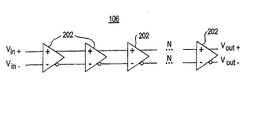
図2は、本発明に従う、等化回路106のブロック図である。図2に示されるように、等化回路106は、「N」個のステージのカスケード202として実施され得る。均等か回路106において実施されるステージの実際の数は、例えば、伝送媒体104によって維持されるデータレート、および、伝送媒体104より予期される減衰量のような要素に依存し得る。例えば、3ステージ等化回路は、6.5Gbpsバックプレーンによって起こる減衰に対して十分に補償し得る。しかし、4ステージ等化回路は、10Gbpsバックプレーンによって起こる減衰に対して補償することを必要とし得る。さらに、一部の実施形態において、等化回路106は、単一のステージ202を有して実施され得る。
FIG. 2 is a block diagram of
図2に示されるように、等化回路106の各ステージ202は、差動入力を受信し、差動出力を出力する。等化回路106が、差動またはシングルエンドであるかは、ドライバ102およびレシーバ108(図1)によって利用されるシリアル通信のタイプによる。例えば、低電圧差動伝送(LVDS)は、差動伝送を利用するシリアル通信規格である。他の実施例において、RS−232は、シングルエンド信号を利用するシリアル通信規格である。本発明は、差動信号を用いるシステムに関連して論議されるが、本発明の原理が、シングルエンド信号を用いるシステムに適用もされ得ることは、当業者によって理解さえるべきである。
As shown in FIG. 2, each
等化回路106の各ステージ202は、周波数応答に従い、入力信号を形付け得る。各ステージ202の周波数応答は、帯域制限型高域フィルター(band−limited high pass filter)の周波数応答と似得る。例えば、等化回路106のステージの周波数応答の大きさは、DCゲインレベルにおいて最初は一定である。第1の「カットオフ」周波数(ここにおいて、ゼロが位置する)において、周波数応答の大きさは、20dB/decadeの速さにおいて増加し始める。等化サーキット106の各ステージ202が、1つのゼロのみを有するように論議されるが、各ステージ202が1つよりも多いゼロを有するように実施され得ることは、当業者によって留意されるべきである。
Each
ステージ202の周波数応答は、1つ以上の極が位置する第2の「カットオフ」周波数において減少し得る。減少のレートは、その周波数に存在する極の数に依存し得、周波数応答の大きさは、存在する各極に対して20dB/decadeの速さにおいて小さくなる。
The frequency response of
等化回路106にある全ステージ202をカスケードすることは、それらのステージの周波数応答特性が一緒に統合することを引き起こす。例えば、2ステージ等化回路の第1のステージが、1GHzにおいて10dBのゲインを提供し、第2のステージが、1GHzにおいて15dBのゲインを提供する場合、1GHz信号に対する2ステージ等化回路の全体的なゲインは、25dBである。
Cascading all
等化回路106の各々のステージ202は、完全にプログラム可能になり得る。ステージ202は、例えば、構成RAMセル、ヒューズベースのデバイス、アンチヒューズ、プログラマブル消去可能読取専用メモリ(PROMS)、消去可能PROMS(EPROMS)、電気的消去可能PROMS(EEPROMS)、フラッシュメモリ、および任意の他の適したデバイスのような構成可能(configurable)デバイスによってプログラム的に制御され得る。一部の実施形態においては、構成可能デバイスは、ステージを制御するために制御信号を格納し得る。
Each
一部の実施形態においては、ステージ202のDCゲインは、プログラム可能になり得る。各々のステージのための構成デバイスは、提供するDCゲインの量をステージに示すために制御信号を格納し得る。DCゲインは、データ信号のピーク間電圧が増えるようにする。例えば、3dBのDCゲインを提供するようにプログラムされているステージが、1GHz信号および10GHz信号を受信した場合、両方の信号のピーク間電圧は、3dB増やされる。
In some embodiments, the DC gain of
一部の実施形態においては、ステージ202のACゲインは、プログラム可能になり得る。ACゲインは、特定の周波数において、そのステージの伝達関数にゼロを挿入することによって提供され得る。ステージ202は、ゼロを挿入するようにプログラム的に制御され得、挿入されたゼロの周波数位置も、プログラム的に制御され得る。
In some embodiments, the AC gain of
上述されたように、ステージ202は、ゼロを挿入するようにプログラム的に制御され得る。等化回路106のあらゆるステージが、ゼロを与える必要はない。例えば、4ステージの等化回路が、低データレートにおいて送信されるデータを等化するために使用された場合、等化回路106が減衰を補償するために、2つのゼロだけが必要になり得る。この実施例においては、4ステージのうちの2つは、ゼロを与えるためにプログラム的に制御され得る。他の2ステージは、ゼロを与えないようにプログラム的に制御され得る。
As described above,
ステージ202がゼロを挿入するようにプログラム的に制御されている場合、周波数応答の大きさは、ゼロの周波数位置から20dB/decade増える。例えば、ゼロが1GHzにおいて挿入された場合、周波数応答の大きさは、1GHzから開始し、20dB/decadeのレートにおいて増える。1GHzにおいて、2つのゼロが挿入された場合、周波数応答の大きさは、1GHzから開始し、40dB/decadeのレートにおいて増える。挿入されるあらゆる追加のゼロは、ゲインが追加の20dB/decade増える、レートを上げる。複数のゼロを挿入することは、等化回路106が、伝送媒体104(図1)に起因する多大の量の減衰を補償することを可能にする。
When
ステージ202によって挿入されるゼロの周波数位置も、プログラム的に制御され得る。ゼロを与える各々のステージ202は、ゼロが他のステージから独立して配置される場所を制御し得る。例えば、ゼロが、ゲインが20dB/decade増えるようにするため、20dBゲインが10GHzにおいて所望された場合、ゼロは、1GHzにおいて挿入され得る。20dBより少ないゲインが所望された場合、ゼロの周波数位置は、10GHzにおけるゲインを減らすために増やされ得る。他の実施例においては、ユーザがバックプレーンの周波数応答を測定し、2.5GHzにおいて極を観測した場合、等化回路106は、極による減衰を消去するために、2.5GHzにおいてゼロを挿入するようにプログラムされ得る。
The zero frequency position inserted by the
一部の実施形態においては、ステージ202は、所定の周波数範囲内にてゼロを挿入することに制限され得る。一部の実施形態において、周波数範囲はプログラム的に制御され得、すなわち、各々のステージに対する周波数上限および下限は、構成可能デバイスによって設定され得る。例えば、ステージ202は、1と1.5GHzとの間にゼロを挿入することに制限され得る(すなわち、1と1.5GHzとの間にゼロを挿入することは、例えば、2GHzのような所望された周波数位置におけるゲインの量を十分に制御する)。ステージ202が、任意の周波数、特に、データ信号を送信するために通常使用される周波数より大きい周波数において、ゼロを挿入することを可能にするのは実用的ではない。
In some embodiments,
構成可能デバイスは、そのステージの所定の周波数範囲内にて2^nの均等に間隔された(evenly−spaced)周波数の1つを選択するために、nビット制御信号をステージに適用し得る。例えば、3ビット制御信号が1と1.5GHzとの間の周波数位置を選択するために使用された場合、制御信号は、1と1.5GHzとの間の8の均等に間隔された周波数から選択し得る。他の実施例においては、4ビット制御信号は、ステージが16の周波数から選択することを可能にする。より多くの制御ビットを提供することは、周波数を選択するのにより高い精度を可能にし得、従って、ステージ202のゲインのより大きな制御を可能にし得る。
The configurable device may apply an n-bit control signal to the stage to select one of 2 ^ n even-spaced frequencies within the predetermined frequency range of the stage. For example, if a 3-bit control signal is used to select a frequency position between 1 and 1.5 GHz, the control signal will be from 8 evenly spaced frequencies between 1 and 1.5 GHz. You can choose. In other embodiments, a 4-bit control signal allows the stage to select from 16 frequencies. Providing more control bits may allow greater accuracy in selecting the frequency and thus allow greater control of the gain of
一部の実施形態においては、所定の制御信号値は、周波数値を選択すること以外の機能のためにリザーブされ得る。例えば、一制御信号値は、ゼロが挿入されるべきではないときを示すためにリザーブされ得る。この実施例においては、残りの2^n−1値は、ゼロを挿入することに対して周波数を選択するためにリザーブされ得る。 In some embodiments, the predetermined control signal value may be reserved for functions other than selecting a frequency value. For example, one control signal value can be reserved to indicate when zero should not be inserted. In this example, the remaining 2 ^ n-1 values can be reserved to select a frequency for inserting zeros.
一部の実施形態においては、等化回路106が複数のステージ202を含む場合、周波数範囲の間にいくつかのオーバラップがあるように、ステージ202の周波数範囲をスタガーすることは有益である。これは、ゼロが、広く、連続的な周波数範囲に渡って挿入されることを可能にする。例えば、第1のステージは、2と3.25GHzとの間にゼロを挿入するように構成され得、第2のステージは、2.75と4GHzとの間にゼロを挿入するように構成され得る。
In some embodiments, if the
更に、ゼロの周波数位置を分散させることは、周波数が増えることによって、周波数応答のスロープを増やし、それによって、等化回路の周波数応答が、周波数が増えることによってスロープがよりネガティブになり、伝送媒体の周波数応答によりきっちりと反対になる(closely counter)ことを可能にする。 Furthermore, the dispersion of the zero frequency position increases the slope of the frequency response by increasing the frequency, thereby making the frequency response of the equalization circuit more negative by increasing the frequency and the transmission medium. Allows the frequency response to be closely countered.
異なる周波数位置において複数のゼロを挿入することも、等化回路106の周波数応答のスロープのより大きな制御を提供する。例えば、等化回路106が、その両方が1GHzにおける、2つのゼロを有する場合、等化回路106は、10GHzにおける40dBのゲインを与える。10GHzにおいて、35dBのゲインだけが所望された場合、両方のゼロの周波数を増やす代わりに、1つのゼロの周波数だけが増やされ得、従って、等化回路106の帯域幅を保存する。
Inserting multiple zeros at different frequency locations also provides greater control of the slope of the frequency response of the
等化回路106は、容量性ローディングも含み得る。一部の実施形態においては、容量性ローディングは、等化回路106の各々のステージに存在し得る。各々のステージ202の容量性ローディングの量は、プログラム的に制御可能になり得る。一部の実施形態においては、容量性ローディングは、等化回路106の出力において存在し得る。等化回路106における容量性ローディングの量は、プログラム的に制御可能になり得る。容量性ローディングの量は、周波数応答がどこでロールオフを開始するかを決定する、等化回路106の伝達関数において、1つ以上の極の周波数位置を決定する。
The
極の周波数位置は、クロストークの減少および/または消去を支援し得る。一部の実施形態においては、極の周波数位置は、データ信号の周波数に設定され得る(例、1Gbpsデータ信号に対して1GHz)。これは、データ信号の周波数以上の周波数を有する信号が、抑制されるようにする(または少なくとも更にブーストされないように)。一部の実施形態においては、極の周波数位置は、高周波信号が増えることから防ぐために、十分に低く設定され得る。クロストーク減少/消去は、高周波ノイズが伝送媒体104(図1)に結合し得た、低周波アプリケーションに使用され得る。 The frequency location of the poles can help reduce and / or eliminate crosstalk. In some embodiments, the pole frequency position may be set to the frequency of the data signal (eg, 1 GHz for a 1 Gbps data signal). This ensures that signals having frequencies above the frequency of the data signal are suppressed (or at least not further boosted). In some embodiments, the pole frequency position can be set low enough to prevent high frequency signals from increasing. Crosstalk reduction / elimination can be used in low frequency applications where high frequency noise could be coupled to the transmission medium 104 (FIG. 1).
図3aは、本発明に従って、等化回路106におけるステージ202の1つによって提供されるプログラム可能ゲイン機能性を示すボード(Bode)図である。一部の実施形態においては、ステージ202によって提供されるゲインの量は、nビット制御信号によって制御される。図3aに示されるように、3ビット制御信号は、等化回路の周波数応答を変化させるために使用される。
FIG. 3a is a board diagram illustrating the programmable gain functionality provided by one of the
一部の実施形態においては、制御信号は、ステージ202がゼロを挿入するのかどうかを決定し、もし挿入するならば、ゼロが挿入される周波数も決定する。例えば、[000]制御信号がステージ202に適用された場合、ステージ202は、その伝達関数にゼロを全く挿入しない。この実施例においては、図3aに示されるように、ステージ202は、[000]制御信号を用いてゲインを全く生成しない。
In some embodiments, the control signal determines whether
[000]以外の制御信号は、ゼロが挿入される周波数を決定し得る。一部の実施形態においては、ステージ202は、周波数の所定の範囲内だけにおいて、ゼロを挿入するように構成され得る。例えば、図3aにおいて、ゼロの周波数位置は、5MHzと50MHzの間である。制御信号は、周波数範囲内において、どこにゼロが挿入されるかを決定し得る。一部の実施形態においては、制御信号のバイアス値が低い場合、ゼロは、周波数範囲の下端の方へ挿入され得る。一部の実施形態においては、制御信号のバイアス値が低い場合、ゼロは、周波数範囲の上端の方へ挿入され得る。この実施例においては、制御信号は、ゼロを挿入する均等に間隔された周波数の7つのうちの1つを選択し得る。
Control signals other than [000] can determine the frequency at which zeros are inserted. In some embodiments,
一般に、ゼロが低周波において挿入された場合、ステージ202は、より多くのゲインを生成する。図3aに示されるように、[111]入力は、[101]入力より多くゲインを生成し、[111]カーブのゼロ挿入ポイントは、[101]カーブのゼロ挿入ポイントより低い周波数にある。
In general, if a zero is inserted at a low frequency, the
どの制御信号をステージ202に適用するかを決定するにおいて、ユーザは、5GHzにおける伝送媒体104(図1)による減衰の量を考慮する。例えば、ユーザが、伝送媒体104の周波数応答を測定し、3GHzデータ信号が6dB減衰することが伝送媒体104に起因することを知った場合、ユーザは、データ信号に6dBのゲインを提供するために、[101]の制御信号を選択し得る。
In deciding which control signal to apply to
図3bおよび図3cは、本発明に従って、等化回路106のプログラム可能スロープ機能性を示すボード図である。
3b and 3c are board diagrams illustrating the programmable slope functionality of the
図3bは、各々のカーブが異なるスロープを有する、カーブ302、304、306、308および310と同様な周波数応答を生成するようにプログラム的に制御され得る、等化回路106を示す。ステージ202は、ゼロを与えるまたはゼロを与えないのどちらかをするように、プログラム的に制御され得る。ゼロを与えるあるゆるステージ202に対して、等化回路106のゲインは、ゼロが追加される周波数から追加の20dB/decade増える。例えば、4ステージ等化回路において、0、20、40、60および80dB/decadeのスロープは、ゼロを与えるステージの数によって、達成され得る。
FIG. 3b shows an
カーブ302のような周波数応答カーブは、等化回路における全てのステージがゼロを与えるようにプログラムされていない場合、達成され得る。カーブ304のような周波数応答は、等化回路におけるステージの1つが、1GHzにおいてゼロを与えるようにプログラムされている場合、達成され得る。同様に、カーブ306、308または310のような周波数応答カーブは、等化回路における2つ、3つまたは4つのステージのそれぞれが、1GHzにおいてゼロを与えるようにプログラムされている場合、達成され得る。
A frequency response curve such as
図3bに示されるように、より大きなスロープを有する周波数応答カーブは、より大きなゲインを達成できる。等化回路106の周波数応答のスロープをプログラム的に制御することは、等化回路106のACゲインの追加の制御を提供する。特に、等化回路106が大きなスロープ(すなわち、複数のゼロ)を有するようにプログラムすることは、等化回路106が、通常複数の極を有し、多大な量の減衰を受ける、伝送媒体104(図1)を通じてのデータの高速送信による減衰を補償することを可能にする。
As shown in FIG. 3b, a frequency response curve with a larger slope can achieve a greater gain. Programmatically controlling the slope of the frequency response of the
図3cは、複数のステージを有する等化回路106のゲインをプログラム的に制御することに対する一アプローチを示す。図3bに示されるように、等化回路106におけるステージ202は、ゼローを挿入するようにプログラム的に制御され得る。周波数応答のスロープにおける複数のゼロの効果を示すために、図3bの中の全てのゼロの周波数位置は、同等の周波数に設定されている。図3cに示されるように、ゼロの周波数位置を変更することは、周波数応答カーブの形においてより大きな制御を提供する。
FIG. 3c shows one approach to programmatically controlling the gain of the
特に、図3cに示されるように、周波数応答カーブ320、322、324、および326は、全て非常に類似している。しかしながら、周波数応答カーブの大きさには明らかな差異がある。例えば、カーブ326の最大ゲインは、20dBを越えるが、カーブ320の最大ゲインは、18dBを越える。他の実施例においては、カーブ320は、2GHzをちょうど越える周波数応答において顕著(noticeable)なベンドを有する。カーブ間のこれらの差異は、異なる周波数位置において挿入されるゼロによるものである。 In particular, as shown in FIG. 3c, the frequency response curves 320, 322, 324, and 326 are all very similar. However, there is a clear difference in the magnitude of the frequency response curve. For example, the maximum gain of curve 326 exceeds 20 dB, while the maximum gain of curve 320 exceeds 18 dB. In other embodiments, curve 320 has a noticeable bend in a frequency response just over 2 GHz. These differences between the curves are due to zeros inserted at different frequency positions.
等化回路が1つよりも多いゼロを与える場合、任意の所定の周波数におけるゲインは、個別のゼロの周波数位置を変更することによって、微同調され得る。ゼロの周波数位置が低くなった場合、全体的なゲインが増える。その一方、そのゼロの周波数位置が増えた場合、全体的なゲインは減る。例えば、図3に示されるように、カーブ320およびカーブ326の両方は、第1の周波数における第1のゼロを有する。カーブ320および326は、第2のゼロも有する。カーブ320の第2のゼロが、カーブ326の第2のゼロより高い周波数位置にあるため、カーブ320はカーブ326より低いゲインを有する。 If the equalization circuit gives more than one zero, the gain at any given frequency can be fine tuned by changing the frequency position of the individual zeros. If the zero frequency position is lowered, the overall gain increases. On the other hand, if the zero frequency position increases, the overall gain decreases. For example, as shown in FIG. 3, both curve 320 and curve 326 have a first zero at a first frequency. Curves 320 and 326 also have a second zero. Curve 320 has a lower gain than curve 326 because the second zero of curve 320 is at a higher frequency position than the second zero of curve 326.
ゼロが異なる周波数位置に挿入されることを可能にすることは、1つの周波数における周波数応答のゲインの制御および周波数応答全体としての形のより高い精度を可能にする。 Allowing zeros to be inserted at different frequency locations allows for gain control of the frequency response at one frequency and higher accuracy of the shape as a whole frequency response.
異なる周波数位置にゼロ挿入することは、等化回路106が、異なる周波数位置に渡って分散される複数の極を有する、伝送媒体104(図1)の減衰をよりきっちりと反対にすることを可能にする。理論的に、等化回路106(図2)は、ゼロが伝送媒体104にある極の周波数位置において挿入された場合、伝送媒体104による全ての周波数に渡る減衰を正確に補償し得る。
Zero insertion at different frequency locations allows the
図3dは、本発明に従って、等化回路によって提供されるクロストークフィルタリング機能性を示す、例示的なボード図である。クロストークは、1つの信号経路からの信号が近くの信号経路に電磁的に結合された場合、生じる。 FIG. 3d is an exemplary board diagram illustrating the crosstalk filtering functionality provided by the equalization circuit in accordance with the present invention. Crosstalk occurs when a signal from one signal path is electromagnetically coupled to a nearby signal path.
等化回路106(図2)の2つの例示的な周波数応答カーブ340および342は、図3dに示される。カーブ340は、クロストークフィルタリングなしの等化回路に対応し、カーブ342は、クロストークフィルタリングを用いた等化回路に対応する。両方のカーブは、1GHzのデータ信号に対して同等の量のゲインを提供する。例えば、1GHzのデータ信号が、4dBの減衰を発生させる伝送媒体を通じて送信された場合、等化回路106は、データ信号をその本来の強さに復帰させるために、周波数応答を有するように構成され得る。
Two exemplary frequency response curves 340 and 342 of the equalization circuit 106 (FIG. 2) are shown in FIG. 3d. A
しかしながら、等化回路106がカーブ340に対応する周波数応答を有するように構成されている場合、近くの信号経路から結合される高周波干渉は、増幅される。これは、近くの信号経路を移動している信号が、ほぼ確実に高周波において送信され、そうでない場合においても、帯域内にない低周波信号は、増幅されないため、低周波アプリケーションにおいては、特に有害である。その一方、等化回路106が、カーブ342に対応する周波数応答を有するように構成されている場合、高周波信号は、かなり減衰される。このアプローチは、クロストークフィルタリングと言及され、等化回路のカットオフ周波数がプログラム的に選択されることを可能にする。一部の実施形態においては、カットオフ周波数は、データ信号が送信される周波数において選択される。これは、等化回路の周波数応答が、データ信号の送信周波数において、頂点に達することを可能にする。
However, when the
クロストークフィルタリングは、ステージ202(図2)の容量性ロードまたは等化回路106の出力におけるステージ202からの別々の容量性ロードとして実施され得る。容量性ローディングの量はプログラム的に制御され得、カットオフ周波数の位置を決定する。一般に、高い容量性ロードが、低いカットオフ周波数という結果になる。容量性ローディングは、周波数の所定の範囲においてロールオフを生成することに制限され得る。
Crosstalk filtering may be implemented as a capacitive load from stage 202 (FIG. 2) or a separate capacitive load from
一部の実施形態においては、mビット制御信号は、等化回路106(図2)が所定の周波数範囲内における2^mの周波数から選択することを可能にするために提供され得る。一部の実施形態においては、mビット制御信号は、等化回路106の周波数応答にロールオフを生成することに対して、2^mの容量性ロード値から選択するために提供され得る。
In some embodiments, an m-bit control signal may be provided to allow the equalization circuit 106 (FIG. 2) to select from 2 ^ m frequencies within a predetermined frequency range. In some embodiments, an m-bit control signal may be provided to select from 2 ^ m capacitive load values for generating a roll-off in the frequency response of the
図4は、本発明に従って、等化回路106を有するレシーバ108のブロック図である。図4に示されるように、等化回路106は、伝送媒体(例、伝送媒体104(図1))を通じて送信されるデータ信号を受信する、レシーバ108に実施される。レシーバ108は、等化回路106の入力に結合されるバイアス回路402、等化回路106の出力に結合されるスライサ404、および等化回路106の出力にも結合されるバッファ406を含み得る。
FIG. 4 is a block diagram of a
バイアス回路402は、バイアス等化回路106にDC電圧を供給する、電圧源408を含み得る。電圧源408は、AC接地(ground)を送信されたデータ信号に提供し得る。バイアス回路402は、抵抗410および412の一致する組も含み得る。一致する抵抗410および412は、等化回路106のインピーダンスを、データがその媒体を通じて送信される伝送媒体104(図1)と一致させるために選択され得る。例えば、伝送媒体104が、50Ω送信ラインである場合、一致するレジスタ410および412の抵抗値は、50Ωに設定されるべきである。設定されない場合、伝送媒体104を通じて送信されるデータ信号は、反射およびパワーロスを受けやすい。一部の実施形態においては、一致するレジスタ410および412の抵抗値は、インピーダンス一致を提供するために、プログラム的に制御され得る。
The
等化回路106がデータ信号を処理した(すなわち、減衰を補償する)後、スライサ404は、フルスケールのデジタル信号を生成するために、等化回路106の出力を処理し得る。スライサ404が一クロックサイクル内にて、等化回路106の出力がロジックハイ(logic high)またはロジックロー(logic low)のどちらを示すのかを決定するように、スライサ404は、デジタルクロックに接続され得る。したがって、スライサ404は、等化回路106の出力からのアナログ信号を、レシーバ108においてデジタル回路によって使用され得るデジタル信号に、本質的に変換する。例えば、レシーバ108がプログラマブルロジックデバイスの一部である場合、スライサ404の出力は、更なる処理のために、プログラマブルロジックデバイスにルートされ得る。
After
一部の実施形態においては、スライサ404は、送信されたデータ信号からクロックおよびデータ情報を回復するために、クロックデータ回復(CDR)回路を含み得る。CDR回路は、正しい量の位相を用いてクロック情報を回復するために、位相ロックループ(PLL)を使用し得る。クロック情報は、次いで、データ信号からデータをサンプリングするために使用され得る。
In some embodiments, the
レシーバ108は、バッファ406をも含み得る。バッファ406は、等化回路106の出力を用いて他の回路をドライブするために使用され得る。バッファ406の入力抵抗は無限であり、従って、等化回路106の出力抵抗に影響しない。バッファ406の出力は、等化回路106の出力抵抗からのそれの抵抗を絶縁させるために、無限ではない入力抵抗を用いて他の回路に結合され得る。バッファ406なしには、等化回路106の帯域幅は、他の回路の入力における任意の容量性ローディングによって影響され得る。そのような容量性ローディングは、等化回路106の周波数応答における極の位置を影響し得る。
The
一部の実施形態においては、バッファ406は、信号検出回路(図示せず)に結合され得る。信号検出回路は、レシーバ108によってデータ信号が受信されているかどうかを検出するために使用され得る。信号検出回路が、入力が受信されていることを検出すると、信号検出回路は、出力信号を生成し得る。出力信号は、スライサ404が受信されたデータ信号を処理できるようにし得る。
In some embodiments, the
一部の実施形態においては、バッファ406は、ループバックバッファ(図示せず)に結合され得る。ループバックバッファは、処理のためにレシーバ108の出力を、他の回路に再度導き得る。例えば、ループバックバッファは、オシロスコープによる観測のために出力をピンにドライブし得る、送信ドライバに、レシーバ108の出力を再度導き得る。他の実施例においては、ループバックバッファは、受信されたデータの有効性(例、ビットエラーレート)を検出するために、レシーバ108の出力を回路に再度導き得る。
In some embodiments,
一部の実施形態においては、バッファ406の出力は、ネガティブフィードバックを等化回路106(図示せず)に提供するために、等化回路106の入力に結合され得、それによって、等化回路106が、出力信号にゲインを適用する(例、フィードバック率に基づいて)ことを可能にする。
In some embodiments, the output of
一部の実施形態においては、バッファ406の出力は、オフセット消去回路(図示せず)に結合され得る。オフセットは、例えば、ステージ202の1つの入力がアンバランスな場合、生じる。例えば、ステージの1つが、差動入力がゼロのときにおいても出力を生成する場合、オフセットは、存在し得る。オフセットは、ステージからステージへと蓄積され得、従って、全てのステージの出力においてオフセットを消去することが好ましい。これは、等化回路106の出力を訂正し、訂正された信号を等化回路106の入力にフィードバックすることによって、達成され得る。
In some embodiments, the output of
上述のものは、本発明の原理を単に例示しているだけであり、様々な修正は、本発明の範囲および精神から逸脱せずに、当業者によって行われ得る。 The foregoing is merely illustrative of the principles of the invention and various modifications can be made by those skilled in the art without departing from the scope and spirit of the invention.
102 ドライバ
104 伝送媒体
106 等化回路
108 レシーバ回路
202 ステージ
404 スライサ
406 バッファ
DESCRIPTION OF
Claims (25)
少なくとも1つの制御デバイスと、
該データ信号に対する等化をプログラム可能に提供する等化回路であって、該データ信号は該等化回路の入力部において受信され、該等化されたデータ信号は該等化回路の出力部において提供され、
該等化回路は、複数のステージを備え、各ステージは、該少なくとも1つの制御デバイスから送信される第1の制御信号を用いて制御され、該第1の制御信号は、nビット制御信号を含み、
該第1の制御信号は、該ステージが、該ステージに関連付けられている周波数範囲内で、該等化回路によって提供されるゲインの傾きを増大させるかどうかを決定し、該ステージが該ゲインの傾きを増大させるように決定された場合に、該第1の制御信号は、該ステージに関連付けられている該周波数範囲内の2^n−1個の選択可能な周波数からの第1の周波数を示し、該データ信号に提供される該ゲインの傾きは、該第1の周波数で増大し、
該第1の周波数は、該少なくとも1つの制御デバイスによってプログラム可能に制御され、それによって、該等化回路は、該伝送媒体によって起こる減衰を補償するために、該データ信号にゲインを提供する、等化回路と、
入力部および出力部を有するバッファであって、該バッファの該入力部は、該等化回路の該出力部に結合されることにより、該バッファに結合された他の回路のインピーダンスを、該等化回路の該出力部インピーダンスから分離し、該バッファの該出力部は、該等化回路の該入力部に結合されることにより、該等化回路にネガティブフィードバック信号を提供し、該等化回路は、該ネガティブフィードバック信号に基づいて、該データ信号に適用されるゲインを調整する、バッファと
を備える、レシーバ回路。 A receiver circuit that receives a data signal transmitted by a driver via a transmission medium, the receiver circuit comprising:
At least one control device;
An equalization circuit for programmably providing equalization for the data signal, wherein the data signal is received at an input of the equalization circuit, and the equalized data signal is received at an output of the equalization circuit Provided,
The equalization circuit includes a plurality of stages, and each stage is controlled using a first control signal transmitted from the at least one control device, and the first control signal includes an n-bit control signal. Including
The first control signal determines whether the stage increases the gain slope provided by the equalization circuit within the frequency range associated with the stage, and the stage If it is determined to increase the slope, the first control signal may select a first frequency from 2 ^ n-1 selectable frequencies within the frequency range associated with the stage. And the slope of the gain provided to the data signal increases at the first frequency;
The first frequency is programmably controlled by the at least one control device so that the equalization circuit provides gain to the data signal to compensate for attenuation caused by the transmission medium; An equalization circuit;
A buffer having an input unit and an output unit, wherein the input unit of the buffer is coupled to the output unit of the equalization circuit so that the impedance of another circuit coupled to the buffer is The output of the buffer is separated from the impedance of the equalizer, and the output of the buffer is coupled to the input of the equalizer to provide a negative feedback signal to the equalizer, the equalizer And a buffer that adjusts a gain applied to the data signal based on the negative feedback signal.
少なくとも1つの制御デバイスと、
該データ信号に対する等化をプログラム可能に提供する等化回路であって、該等化回路は、複数のステージを備え、各ステージは、該少なくとも1つの制御デバイスから送信される制御信号を用いて制御され、該制御信号は、nビット制御信号を含み、
該制御信号は、該ステージが、該ステージに関連付けられている周波数範囲内で、該等化回路によって提供されるゲインの傾きを増大させるかどうかを決定し、該ステージが周波数応答の該ゲインの傾きを増大させるように決定された場合に、該制御信号は、該ステージに関連付けられている該周波数範囲内の2^n−1個の選択可能な周波数からの第1の周波数を示し、該ゲインの傾きは、該第1の周波数で増大し、
該第1の周波数は、該少なくとも1つの制御デバイスによってプログラム可能に制御され、それによって、該等化回路は、該伝送媒体によって起こる減衰を補償するために、該データ信号にゲインを提供する、等化回路と、
該等化回路の出力部に結合されたスライサであって、該スライサに複数のクロックサイクルを提供するデジタルクロックに結合され、該スライサは、該複数のクロックサイクルのうちの1つ内の該データ信号が高い場合にデジタル高信号を割り当て、該複数のクロックサイクルのうちの1つ内の該データ信号が低い場合にデジタル低信号を割り当てることによって、該データ信号をデジタル信号へ変換し、該スライサは、該データ信号からクロックおよびデータ情報を抽出するクロックデータリカバリ回路を備える、スライサと
を備える、レシーバ回路。 A receiver circuit that receives a data signal transmitted by a driver via a transmission medium, the receiver circuit comprising:
At least one control device;
An equalization circuit that programmably provides equalization for the data signal, the equalization circuit comprising a plurality of stages, each stage using a control signal transmitted from the at least one control device Controlled, the control signal includes an n-bit control signal;
The control signal determines whether the stage increases the slope of the gain provided by the equalization circuit within the frequency range associated with the stage, and the stage determines the gain of the frequency response. When determined to increase the slope, the control signal indicates a first frequency from 2 ^ n-1 selectable frequencies within the frequency range associated with the stage ; The gain slope increases at the first frequency,
The first frequency is programmably controlled by the at least one control device so that the equalization circuit provides gain to the data signal to compensate for attenuation caused by the transmission medium; An equalization circuit;
A slicer coupled to an output of the equalization circuit, coupled to a digital clock that provides a plurality of clock cycles to the slicer, wherein the slicer includes the data in one of the plurality of clock cycles. Converting the data signal to a digital signal by assigning a digital high signal when the signal is high and assigning a digital low signal when the data signal in one of the plurality of clock cycles is low; Comprises a slicer comprising a clock data recovery circuit for extracting clock and data information from the data signal.
第1および第2のステージを有する等化器を提供することと、
該第1および第2のステージの各々に対する少なくとも1つの制御デバイスが、該ステージによって該データ信号に提供されるゲインの傾きが、該ステージに関連付けられている周波数範囲内で増大するかどうかを決定するために該ステージに制御信号を送信することであって、該制御信号は、nビット制御信号を含み、該制御信号は、該ステージに関連付けられている該周波数範囲内の2^n−1個の選択可能な周波数から1つの周波数を決定するためのものであり、該ゲインの傾きが増大すると決定された場合に、該ゲインの傾きは該1つの周波数で増大する、ことと、
該第1のステージに対して、該ゲインの傾きが増大可能な第1の周波数範囲を規定すること、および、該第2のステージに対して、該ゲインの傾きが増大可能な第2の周波数範囲を規定することであって、該第1の周波数範囲が該第2の周波数範囲とオーバーラップし、それによって、該オーバーラップする該第1の周波数範囲と該第2の周波数範囲とは、一緒に、該第1の周波数範囲および該第2の周波数範囲のうちのいずれの1つよりも広い連続的な周波数範囲をカバーする、ことと、
該少なくとも1つの制御デバイスが、該1つの周波数をプログラム可能に制御することであって、それによって、該第1のステージと該第2のステージとが該伝送媒体によって起こる減衰を補償するために十分なゲインを提供する、ことと、
等化されたデータ信号を生成するために、該第1のステージと該第2のステージとに該データ信号を適用することと
を包含する、方法。 A method for providing equalization for a data signal transmitted over a transmission medium, the method comprising:
Providing an equalizer having first and second stages;
At least one control device for each of the first and second stages determines whether the slope of the gain provided by the stage to the data signal increases within the frequency range associated with the stage. Transmitting a control signal to the stage, the control signal including an n-bit control signal, the control signal being 2 ^ n−1 within the frequency range associated with the stage. It is for determining one of the frequencies from the number of selectable frequency, if the slope of the gain is determined to be increased, the slope of the gain is increased at the one frequency, and that,
Defining a first frequency range in which the gain slope can be increased with respect to the first stage; and a second frequency at which the gain slope can be increased with respect to the second stage. Defining a range, wherein the first frequency range overlaps the second frequency range, whereby the overlapping first frequency range and the second frequency range are: Together covering a continuous frequency range wider than any one of the first frequency range and the second frequency range;
The at least one control device, the method comprising programmably controlling the single frequency, thereby to the first stage and the second stage to compensate for the attenuation caused by said transmission medium Providing enough gain, and
Applying the data signal to the first stage and the second stage to generate an equalized data signal.
制御デバイスから送信される制御信号を用いて制御されるステージを備え、
該制御信号は、該ステージが、該ステージに関連付けられている周波数範囲内で、該等化回路によって提供されるゲインの傾きを増大させるかどうかを決定し、該制御信号は、nビット制御信号を含み、該ステージが該ゲインの傾きを増大させることが決定された場合に、該制御信号は、該ステージに関連付けられている該周波数範囲内の2^n−1個の選択可能な周波数からの第1の周波数を示し、該ゲインの傾きは、該第1の周波数で増大し、
該第1の周波数は、該制御デバイスによってプログラム可能に制御され、それによって、該等化回路は、該伝送媒体によって起こる減衰を補償するために、該データ信号にゲインを提供する、等化回路。 An equalization circuit for providing equalization to a received data signal, the data signal being received at an input of the equalization circuit via a transmission medium, the equalization circuit comprising:
Comprising a stage controlled using a control signal transmitted from the control device;
The control signal determines whether the stage increases the slope of the gain provided by the equalization circuit within the frequency range associated with the stage, the control signal is an n-bit control signal And when the stage is determined to increase the slope of the gain, the control signal is derived from 2 ^ n-1 selectable frequencies within the frequency range associated with the stage. The gain slope increases at the first frequency,
The first frequency is programmably controlled by the control device so that the equalization circuit provides gain to the data signal to compensate for attenuation caused by the transmission medium .
前記1つの周波数をプログラム可能に制御することは、該ステージが前記ゲインの傾きを増大させるように決定された場合に、該1つの周波数で該ステージによって提供される該ゲインの傾きを増大させることを包含する、請求項13に記載の方法。 At least one of the first and second stages further comprising receiving the control signal from the at least one control device;
Controlling the previous SL one frequency programmably, when the stage is determined so as to increase the inclination of the gain, increases the slope of the gain provided by the stage in said one frequency 14. The method of claim 13, comprising:
少なくとも1つの制御デバイスと、
該データ信号に対する等化をプログラム可能に提供する等化回路であって、該データ信号は該等化回路の入力部において受信され、該等化されたデータ信号は該等化回路の出力部において提供され、
該等化回路は、複数のステージを備え、各ステージは、該少なくとも1つの制御デバイスから送信される制御信号を用いて制御され、該制御信号は、nビット制御信号を含み、
該制御信号は、該ステージが、該ステージに関連付けられている周波数範囲内で、該等化回路によって提供されるゲインの傾きを増大させるかどうかを決定し、該ステージが該ゲインの傾きを増大させるように決定された場合に、該制御信号は、該ステージに関連付けられている該周波数範囲内の2^n−1個の選択可能な周波数からの第1の周波数を示し、該データ信号に提供される該ゲインの傾きは、該第1の周波数で増大し、
該制御信号によって示される該第1の周波数は、該少なくとも1つの制御デバイスによってプログラム可能に制御され、それによって、該ステージが該第1の周波数で該ゲインの傾きを増大する場合に、該等化回路は、該伝送媒体によって起こる減衰を補償するために、該データ信号にゲインを提供する、等化回路と、
入力部および出力部を有するバッファであって、該バッファの該入力部は、該等化回路の該出力部に結合されることにより、該バッファに結合された他の回路のインピーダンスを、該等化回路の該出力部インピーダンスから分離し、該バッファの該出力部は、該等化回路の該入力部に結合されることにより、該等化回路にネガティブフィードバック信号を提供し、該等化回路は、該ネガティブフィードバック信号に基づいて、該データ信号に提供されるゲインを調整する、バッファと
該等化回路の入力部に結合されたバイアス回路であって、該バイアス回路は、該データ信号にDCバイアシングを提供して該伝送媒体とマッチングするインピーダンスを提供するように構成される、バイアス回路と
を備える、レシーバ回路。 A receiver circuit that receives a data signal transmitted by a driver via a transmission medium, the receiver circuit comprising:
At least one control device;
An equalization circuit for programmably providing equalization for the data signal, wherein the data signal is received at an input of the equalization circuit, and the equalized data signal is received at an output of the equalization circuit Provided,
The equalization circuit comprises a plurality of stages, each stage being controlled using a control signal transmitted from the at least one control device, the control signal comprising an n-bit control signal;
The control signal determines whether the stage increases the gain slope provided by the equalization circuit within the frequency range associated with the stage, and the stage increases the gain slope. The control signal indicates a first frequency from 2 ^ n-1 selectable frequencies within the frequency range associated with the stage , and the data signal The provided slope of gain increases at the first frequency;
The first frequency indicated by the control signal is programmably controlled by the at least one control device so that the stage increases the slope of the gain at the first frequency. An equalizer circuit that provides gain to the data signal to compensate for attenuation caused by the transmission medium;
A buffer having an input unit and an output unit, wherein the input unit of the buffer is coupled to the output unit of the equalization circuit so that the impedance of another circuit coupled to the buffer is The output of the buffer is separated from the impedance of the equalizer, and the output of the buffer is coupled to the input of the equalizer to provide a negative feedback signal to the equalizer, the equalizer Is a bias circuit coupled to the input of the buffer and the equalization circuit that adjusts the gain provided to the data signal based on the negative feedback signal, the bias circuit receiving the data signal And a bias circuit configured to provide DC biasing to provide impedance matching the transmission medium.
少なくとも1つの制御デバイスと、
該データ信号に対する等化をプログラム可能に提供する等化回路であって、
該等化回路は、複数のステージを備え、各ステージは、該少なくとも1つの制御デバイスから送信される制御信号を用いて制御され、
該制御信号は、該ステージが、該ステージに関連付けられている周波数範囲内で、該等化回路によって提供されるゲインの傾きを増大させるかどうかを決定し、該制御信号は、nビット制御信号を含み、該ステージが周波数応答の該ゲインの傾きを増大させるように決定された場合に、該制御信号は、該ステージに関連付けられている該周波数範囲内の2^n−1個の選択可能な周波数からの第1の周波数を示し、該データ信号に提供される該ゲインの傾きは、該第1の周波数で増大し、
該制御信号によって示される該第1の周波数は、該少なくとも1つの制御デバイスによってプログラム可能に制御され、それによって、該等化回路は、該伝送媒体によって起こる減衰を補償するために、該データ信号にゲインを提供する、等化回路と、
該等化回路の出力部に結合されたスライサであって、該スライサに複数のクロックサイクルを提供するデジタルクロックに結合され、該スライサは、該複数のクロックサイクルのうちの1つ内の該データ信号が高い場合にデジタル高信号を割り当て、該複数のクロックサイクルのうちの1つ内の該データ信号が低い場合にデジタル低信号を割り当てることによって、該データ信号をデジタル信号へ変換し、該スライサは、該データ信号からクロックおよびデータ情報を抽出するクロックデータリカバリ回路を備える、スライサと
該等化回路の入力部に結合されたバイアス回路であって、該バイアス回路は、
該データ信号にDCバイアシングを提供して該伝送媒体とマッチングするインピーダンスを提供するように構成される、バイアス回路と
を備える、レシーバ回路。 A receiver circuit that receives a data signal transmitted by a driver via a transmission medium, the receiver circuit comprising:
At least one control device;
An equalization circuit for programmably providing equalization for the data signal,
The equalization circuit comprises a plurality of stages, each stage being controlled using a control signal transmitted from the at least one control device;
The control signal determines whether the stage increases the slope of the gain provided by the equalization circuit within the frequency range associated with the stage, the control signal is an n-bit control signal And the control signal is selectable 2 ^ n-1 within the frequency range associated with the stage, if the stage is determined to increase the slope of the gain of the frequency response The gain slope provided to the data signal increases at the first frequency,
The first frequency indicated by the control signal is programmably controlled by the at least one control device so that the equalization circuit is configured to compensate for the attenuation caused by the transmission medium. An equalization circuit that provides gain to
A slicer coupled to an output of the equalization circuit, coupled to a digital clock that provides a plurality of clock cycles to the slicer, wherein the slicer includes the data in one of the plurality of clock cycles. Converting the data signal to a digital signal by assigning a digital high signal when the signal is high and assigning a digital low signal when the data signal in one of the plurality of clock cycles is low; Is a bias circuit coupled to the input of the slicer and the equalization circuit, comprising a clock data recovery circuit for extracting clock and data information from the data signal, the bias circuit comprising:
A bias circuit configured to provide DC biasing to the data signal to provide impedance matching the transmission medium.
該データ信号へのDCバイアシングを提供して該伝送媒体とマッチングするインピーダンススを適用することと、
第1および第2のステージを有する等化器を提供することと、
該第1および第2のステージの各々に対する制御デバイスが、該ステージによって該データ信号に提供されるゲインの傾きが、該ステージに関連付けられている周波数範囲内で増大するかどうかを決定するために該ステージに制御信号を送信することであって、該制御信号は、nビット制御信号を含み、該制御信号は、該ステージに関連付けられている該周波数範囲内の2^n−1個の選択可能な周波数から1つの周波数を決定するためのものであり、該ゲインの傾きが増大すると決定された場合に、該ゲインの傾きは該1つの周波数で増大する、ことと、
該第1のステージに対して、該ゲインの傾きが増大可能な第1の周波数範囲を規定すること、および、該第2のステージに対して、該ゲインの傾きが増大可能な第2の周波数範囲を規定することであって、該第1の周波数範囲が該第2の周波数範囲とオーバーラップし、それによって、該オーバーラップする該第1の周波数範囲と該第2の周波数範囲とは、該第1の周波数範囲および該第2の周波数範囲のうちのいずれの1つよりも広い連続的な周波数範囲をカバーする、ことと、
該制御デバイスが、該1つの周波数を制御することであって、それによって、該第1のステージと該第2のステージとが該伝送媒体によって起こる減衰を補償するために十分なゲインを提供する、ことと、
等化されたデータ信号を生成するために、該第1のステージと該第2のステージとに該データ信号を適用することと
を包含する、方法。 A method for providing equalization for a data signal transmitted over a transmission medium, the method comprising:
Applying DC biasing to the data signal to apply impedance matching the transmission medium;
Providing an equalizer having first and second stages;
A control device for each of the first and second stages to determine whether the slope of the gain provided by the stage to the data signal increases within the frequency range associated with the stage Transmitting a control signal to the stage, the control signal comprising an n-bit control signal, the control signal being 2 ^ n-1 selections within the frequency range associated with the stage are found from possible frequency for determining one of the frequencies, when the slope of the gain is determined to be increased, the slope of the gain is increased at the one frequency, and that,
Defining a first frequency range in which the gain slope can be increased with respect to the first stage; and a second frequency at which the gain slope can be increased with respect to the second stage. Defining a range, wherein the first frequency range overlaps the second frequency range, whereby the overlapping first frequency range and the second frequency range are: Covering a continuous frequency range wider than any one of the first frequency range and the second frequency range;
Control device, the method comprising controlling the one frequency, whereby the said first stage and the second stage provides sufficient gain to compensate for attenuation caused by said transmission medium , That,
Applying the data signal to the first stage and the second stage to generate an equalized data signal.
Applications Claiming Priority (2)
| Application Number | Priority Date | Filing Date | Title |
|---|---|---|---|
| US11/182,658 | 2005-07-14 | ||
| US11/182,658 US7697600B2 (en) | 2005-07-14 | 2005-07-14 | Programmable receiver equalization circuitry and methods |
Related Child Applications (1)
| Application Number | Title | Priority Date | Filing Date |
|---|---|---|---|
| JP2012022868A Division JP5529904B2 (en) | 2005-07-14 | 2012-02-06 | Programmable receiver equalization circuit and method |
Publications (3)
| Publication Number | Publication Date |
|---|---|
| JP2007028625A JP2007028625A (en) | 2007-02-01 |
| JP2007028625A5 JP2007028625A5 (en) | 2009-08-20 |
| JP4989931B2 true JP4989931B2 (en) | 2012-08-01 |
Family
ID=37198748
Family Applications (2)
| Application Number | Title | Priority Date | Filing Date |
|---|---|---|---|
| JP2006193262A Expired - Fee Related JP4989931B2 (en) | 2005-07-14 | 2006-07-13 | Programmable receiver equalization circuit and method |
| JP2012022868A Expired - Fee Related JP5529904B2 (en) | 2005-07-14 | 2012-02-06 | Programmable receiver equalization circuit and method |
Family Applications After (1)
| Application Number | Title | Priority Date | Filing Date |
|---|---|---|---|
| JP2012022868A Expired - Fee Related JP5529904B2 (en) | 2005-07-14 | 2012-02-06 | Programmable receiver equalization circuit and method |
Country Status (4)
| Country | Link |
|---|---|
| US (1) | US7697600B2 (en) |
| EP (2) | EP1744510B1 (en) |
| JP (2) | JP4989931B2 (en) |
| CN (1) | CN1897474B (en) |
Families Citing this family (21)
| Publication number | Priority date | Publication date | Assignee | Title |
|---|---|---|---|---|
| EP1447950A1 (en) * | 2003-02-14 | 2004-08-18 | Vrije Universiteit Brussel | Low voltage adaptive equalizer |
| US7760799B2 (en) * | 2005-09-28 | 2010-07-20 | Altera Corporation | Programmable digital equalization control circuitry and methods |
| WO2008062374A2 (en) * | 2006-11-23 | 2008-05-29 | Nxp B.V. | Single communication channel between a contactless frontend device and a transceiver device |
| US7782088B1 (en) | 2007-02-15 | 2010-08-24 | Altera Corporation | Sharing adaptive dispersion compensation engine among programmable logic device serial interface channels |
| US8208528B1 (en) | 2007-12-13 | 2012-06-26 | Altera Corporation | Programmable adaptation convergence detection |
| US8989214B2 (en) * | 2007-12-17 | 2015-03-24 | Altera Corporation | High-speed serial data signal receiver circuitry |
| US8175143B1 (en) | 2008-02-26 | 2012-05-08 | Altera Corporation | Adaptive equalization using data level detection |
| US8558955B2 (en) * | 2008-11-03 | 2013-10-15 | Intersil Americas Inc. | Cable equalization locking |
| JP5664295B2 (en) * | 2011-02-03 | 2015-02-04 | 富士通株式会社 | Communication device and communication device setting method |
| US8937990B2 (en) * | 2012-08-31 | 2015-01-20 | Fujitsu Limited | Low-frequency equalizer circuit for a high-speed broadband signal |
| US9608728B1 (en) | 2014-01-24 | 2017-03-28 | Altera Corporation | Integrated circuit device with field programmable optical array |
| CN106105122B (en) * | 2014-03-20 | 2019-07-16 | 三菱电机株式会社 | Processing circuit and signal calibration method |
| US9350529B1 (en) * | 2015-03-23 | 2016-05-24 | Realtek Semiconductor Corp. | Method and apparatus for detecting logical signal |
| TWI599172B (en) * | 2015-03-09 | 2017-09-11 | 瑞昱半導體股份有限公司 | Method and apparatus for detecting logical signal |
| KR102409823B1 (en) * | 2017-08-17 | 2022-06-17 | 삼성디스플레이 주식회사 | Display panel driver and display apparatus having the same |
| CN109831398B (en) * | 2018-12-29 | 2021-11-26 | 晶晨半导体(上海)股份有限公司 | Automatic adjusting method for gain of multistage equalizer of serial data receiver |
| US11575437B2 (en) * | 2020-01-10 | 2023-02-07 | Macom Technology Solutions Holdings, Inc. | Optimal equalization partitioning |
| TW202143665A (en) * | 2020-01-10 | 2021-11-16 | 美商Macom技術方案控股公司 | Optimal equalization partitioning |
| US11206161B1 (en) | 2020-09-16 | 2021-12-21 | Nxp B.V. | Adaptive equilizer and gain controller |
| US11177986B1 (en) * | 2020-11-24 | 2021-11-16 | Texas Instruments Incorporated | Lane adaptation in high-speed serial links |
| CN114338310A (en) * | 2021-12-29 | 2022-04-12 | 苏州芯格微电子有限公司 | Programmable high-frequency high-gain equalizer for digital display interface and gain method |
Family Cites Families (27)
| Publication number | Priority date | Publication date | Assignee | Title |
|---|---|---|---|---|
| US3568100A (en) * | 1967-12-26 | 1971-03-02 | Bell Telephone Labor Inc | Automatic equalizer for digital transmission systems |
| JPS593898B2 (en) * | 1978-02-28 | 1984-01-26 | 富士通株式会社 | Communication method |
| US4430744A (en) * | 1981-12-18 | 1984-02-07 | Gte Automatic Electric Incorporated | Adaptive IF equalizer for digital transmission |
| JPS6162241A (en) * | 1984-09-04 | 1986-03-31 | Nec Corp | Automatic railway equalizer of switched capacitor |
| JPS62274936A (en) * | 1986-05-23 | 1987-11-28 | Meidensha Electric Mfg Co Ltd | Waveform reproducing circuit for transmission signal |
| US4887278A (en) * | 1986-07-29 | 1989-12-12 | Integrated Network Corporation | Equalizer for digital transmission systems |
| JPH0683111B2 (en) * | 1987-12-24 | 1994-10-19 | 富士通株式会社 | ▲ √f ▼ Automatic gain control amplifier |
| JP2830087B2 (en) * | 1989-06-30 | 1998-12-02 | ソニー株式会社 | Frequency characteristic correction circuit |
| US5257286A (en) * | 1990-11-13 | 1993-10-26 | Level One Communications, Inc. | High frequency receive equalizer |
| JP3217079B2 (en) * | 1991-02-14 | 2001-10-09 | 株式会社日立製作所 | Semiconductor integrated circuit |
| US5717715A (en) * | 1995-06-07 | 1998-02-10 | Discovision Associates | Signal processing apparatus and method |
| US5642079A (en) * | 1995-09-29 | 1997-06-24 | Dallas Semiconductor Corporation | Amplifier with pole/zero compensation |
| JP3576702B2 (en) * | 1996-06-12 | 2004-10-13 | 富士通株式会社 | Variable high-pass filter |
| US6303922B1 (en) * | 1997-07-21 | 2001-10-16 | Ortel Corporation | Range-switching optical receiver with high sensitivity and wide dynamic range |
| KR19990084784A (en) * | 1998-05-11 | 1999-12-06 | 윤종용 | P.G., narrowband noise canceller and ultrafast digital subscriber line receiver having them |
| US6249544B1 (en) * | 1998-11-13 | 2001-06-19 | Broadcom Corporation | System and method for high-speed decoding and ISI compensation in a multi-pair transceiver system |
| US6424480B1 (en) * | 1999-09-28 | 2002-07-23 | Koninklijke Philips Electronics N.V. | Magnetic medium storage apparatus with read channel having a programmable write-to-read suppression |
| US20040138876A1 (en) * | 2003-01-10 | 2004-07-15 | Nokia Corporation | Method and apparatus for artificial bandwidth expansion in speech processing |
| US7164711B2 (en) * | 2003-01-22 | 2007-01-16 | Agere Systems Inc. | Programmable receive-side channel equalizer |
| US6870404B1 (en) * | 2003-08-28 | 2005-03-22 | Altera Corporation | Programmable differential capacitors for equalization circuits |
| CN100556011C (en) * | 2003-09-23 | 2009-10-28 | Nxp股份有限公司 | Sef-adapting filter |
| US7239849B2 (en) * | 2003-11-04 | 2007-07-03 | Altera Corporation | Adaptive communication methods and apparatus |
| US7272178B2 (en) * | 2003-12-08 | 2007-09-18 | Freescale Semiconductor, Inc. | Method and apparatus for controlling the bandwidth frequency of an analog filter |
| US7233164B2 (en) * | 2003-12-17 | 2007-06-19 | Rambus Inc. | Offset cancellation in a multi-level signaling system |
| JP2005223877A (en) * | 2004-01-05 | 2005-08-18 | Renesas Technology Corp | High-frequency power amplifier circuit |
| US6894632B1 (en) * | 2004-01-14 | 2005-05-17 | Northrop Grumman Corporation | Programmable analog-to-digital converter |
| EP1615351A1 (en) * | 2004-07-09 | 2006-01-11 | Vrije Universiteit Brussel | Multistage equalizer |
-
2005
- 2005-07-14 US US11/182,658 patent/US7697600B2/en not_active Expired - Fee Related
-
2006
- 2006-07-10 EP EP06014235.3A patent/EP1744510B1/en active Active
- 2006-07-10 EP EP13175861.7A patent/EP2658197B1/en active Active
- 2006-07-13 JP JP2006193262A patent/JP4989931B2/en not_active Expired - Fee Related
- 2006-07-14 CN CN2006101018987A patent/CN1897474B/en not_active Expired - Fee Related
-
2012
- 2012-02-06 JP JP2012022868A patent/JP5529904B2/en not_active Expired - Fee Related
Also Published As
| Publication number | Publication date |
|---|---|
| EP2658197B1 (en) | 2018-09-19 |
| CN1897474A (en) | 2007-01-17 |
| EP1744510B1 (en) | 2018-09-05 |
| US20070014344A1 (en) | 2007-01-18 |
| JP2012130047A (en) | 2012-07-05 |
| JP2007028625A (en) | 2007-02-01 |
| EP1744510A3 (en) | 2009-09-09 |
| EP2658197A2 (en) | 2013-10-30 |
| EP2658197A3 (en) | 2014-04-02 |
| CN1897474B (en) | 2012-07-18 |
| US7697600B2 (en) | 2010-04-13 |
| EP1744510A2 (en) | 2007-01-17 |
| JP5529904B2 (en) | 2014-06-25 |
Similar Documents
| Publication | Publication Date | Title |
|---|---|---|
| JP4989931B2 (en) | Programmable receiver equalization circuit and method | |
| US9705708B1 (en) | Integrated circuit with continuously adaptive equalization circuitry | |
| US6794900B2 (en) | Method and circuit for pre-emphasis equalization in high speed data communications | |
| US7702011B2 (en) | High-speed serial data receiver architecture | |
| US7974337B2 (en) | High speed receive equalizer architecture | |
| EP1806850B1 (en) | Signal adjustment receiver circuitry | |
| US9172566B1 (en) | Methods and apparatus for multiple-stage CTLE adaptation | |
| JP2007028625A5 (en) | ||
| US20040239369A1 (en) | Programmable peaking receiver and method | |
| US9917707B2 (en) | Adaptive cascaded equalization circuits with configurable roll-up frequency response for spectrum compensation | |
| US10284394B1 (en) | Input termination circuits for high speed receivers | |
| CN115051718A (en) | De-emphasis controller for transmit driver in wired communication | |
| US9602318B2 (en) | Closed-loop high-speed channel equalizer adaptation | |
| US20080253439A1 (en) | De-emphasizing cable equalizer | |
| US20040141552A1 (en) | Programmable receive-side channel equalizer | |
| EP2733897A2 (en) | Apparatus and methods for adaptive receiver delay equalization | |
| US7804892B1 (en) | Circuitry for providing programmable decision feedback equalization | |
| US7190719B2 (en) | Impedance controlled transmitter with adaptive compensation for chip-to-chip communication | |
| EP2127330A1 (en) | Multi-stage differential warping amplifier and method | |
| CN101478323A (en) | Methods and apparatus for improved jitter tolerance in an SFP limit amplified signal | |
| EP1445903A2 (en) | Serial digital data communications receiver with improved automatic cable equalizer and DC restorer |
Legal Events
| Date | Code | Title | Description |
|---|---|---|---|
| A521 | Request for written amendment filed |
Free format text: JAPANESE INTERMEDIATE CODE: A523 Effective date: 20090703 |
|
| A621 | Written request for application examination |
Free format text: JAPANESE INTERMEDIATE CODE: A621 Effective date: 20090703 |
|
| A521 | Request for written amendment filed |
Free format text: JAPANESE INTERMEDIATE CODE: A523 Effective date: 20100630 |
|
| A131 | Notification of reasons for refusal |
Free format text: JAPANESE INTERMEDIATE CODE: A131 Effective date: 20110124 |
|
| A601 | Written request for extension of time |
Free format text: JAPANESE INTERMEDIATE CODE: A601 Effective date: 20110425 |
|
| A602 | Written permission of extension of time |
Free format text: JAPANESE INTERMEDIATE CODE: A602 Effective date: 20110428 |
|
| A521 | Request for written amendment filed |
Free format text: JAPANESE INTERMEDIATE CODE: A523 Effective date: 20110511 |
|
| A02 | Decision of refusal |
Free format text: JAPANESE INTERMEDIATE CODE: A02 Effective date: 20111011 |
|
| A521 | Request for written amendment filed |
Free format text: JAPANESE INTERMEDIATE CODE: A523 Effective date: 20120206 |
|
| A911 | Transfer to examiner for re-examination before appeal (zenchi) |
Free format text: JAPANESE INTERMEDIATE CODE: A911 Effective date: 20120213 |
|
| TRDD | Decision of grant or rejection written | ||
| A01 | Written decision to grant a patent or to grant a registration (utility model) |
Free format text: JAPANESE INTERMEDIATE CODE: A01 Effective date: 20120329 |
|
| A01 | Written decision to grant a patent or to grant a registration (utility model) |
Free format text: JAPANESE INTERMEDIATE CODE: A01 |
|
| A61 | First payment of annual fees (during grant procedure) |
Free format text: JAPANESE INTERMEDIATE CODE: A61 Effective date: 20120501 |
|
| R150 | Certificate of patent or registration of utility model |
Free format text: JAPANESE INTERMEDIATE CODE: R150 |
|
| FPAY | Renewal fee payment (event date is renewal date of database) |
Free format text: PAYMENT UNTIL: 20150511 Year of fee payment: 3 |
|
| R250 | Receipt of annual fees |
Free format text: JAPANESE INTERMEDIATE CODE: R250 |
|
| R250 | Receipt of annual fees |
Free format text: JAPANESE INTERMEDIATE CODE: R250 |
|
| R250 | Receipt of annual fees |
Free format text: JAPANESE INTERMEDIATE CODE: R250 |
|
| LAPS | Cancellation because of no payment of annual fees |