JP4986291B2 - Superconducting cable - Google Patents
Superconducting cable Download PDFInfo
- Publication number
- JP4986291B2 JP4986291B2 JP2007211069A JP2007211069A JP4986291B2 JP 4986291 B2 JP4986291 B2 JP 4986291B2 JP 2007211069 A JP2007211069 A JP 2007211069A JP 2007211069 A JP2007211069 A JP 2007211069A JP 4986291 B2 JP4986291 B2 JP 4986291B2
- Authority
- JP
- Japan
- Prior art keywords
- superconducting
- layer
- composite wire
- tape
- cable
- Prior art date
- Legal status (The legal status is an assumption and is not a legal conclusion. Google has not performed a legal analysis and makes no representation as to the accuracy of the status listed.)
- Expired - Fee Related
Links
Images


Classifications
-
- Y—GENERAL TAGGING OF NEW TECHNOLOGICAL DEVELOPMENTS; GENERAL TAGGING OF CROSS-SECTIONAL TECHNOLOGIES SPANNING OVER SEVERAL SECTIONS OF THE IPC; TECHNICAL SUBJECTS COVERED BY FORMER USPC CROSS-REFERENCE ART COLLECTIONS [XRACs] AND DIGESTS
- Y02—TECHNOLOGIES OR APPLICATIONS FOR MITIGATION OR ADAPTATION AGAINST CLIMATE CHANGE
- Y02E—REDUCTION OF GREENHOUSE GAS [GHG] EMISSIONS, RELATED TO ENERGY GENERATION, TRANSMISSION OR DISTRIBUTION
- Y02E40/00—Technologies for an efficient electrical power generation, transmission or distribution
- Y02E40/60—Superconducting electric elements or equipment; Power systems integrating superconducting elements or equipment
Description
本発明は、長距離大容量の送電用として使用される超電導ケーブルに関し、特に、厚みを薄くした超電導テープにより形成される超電導層を備えた超電導ケーブルに関する。 The present invention relates to a superconducting cable used for long-distance and large-capacity power transmission, and more particularly to a superconducting cable including a superconducting layer formed of a superconducting tape having a reduced thickness.
超電導テープとして、Bi-Sr-Ca-Cu-Oテープ線材に代表されるBi系超電導テープが実用化されつつある。このBi系超電導テープは、例えばBi2223相からなる複数本の超電導フィラメントを銀などの安定化材中に埋設した構造のテープ線材である。その断面は、例えば図4に示すように、Bi系酸化物超電導体からなる多数本の超電導フィラメント21bを銀材等からなる金属シース(金属安定化材)21aで覆ってテープ状に形成される。このBi系超電導テープ21により、例えば図5に示すようなケーブルコア9が形成される。即ち、ケーブルコア9は、Cuなどの常電導材料からなる素線を撚り合せた撚り線又は中空パイプ等で構成されるフォーマ1の外周に層間絶縁16を介して巻回される複数層のBi系超電導テープ21によって形成される超電導導体層2と、その外周に巻回されるクラフト紙やクラフト紙とポリオレフィンフィルムをラミネートした複合紙等からなる絶縁層3と、その外周に層間絶縁17を介して巻回される複数層のBi系超電導テープ21からなる超電導シールド層4と、その外周に層間絶縁17を介して巻回される外層18とで形成される。このようなケーブルコア9は、その軸方向に引張力を作用させた状態下で3本が強制的に撚り合わされて、例えば図6に示すように、内管6と外管7で形成される二重断熱管内に挿入され、内管6内に冷媒流通路5が形成される。外管7は防食層8によって覆われ、内管6と外管7の間は真空引きされて真空層とされる。このようにして、交流用の3心一括型の超電導ケーブル10が形成される。
As a superconducting tape, a Bi-based superconducting tape represented by a Bi-Sr-Ca-Cu-O tape wire is being put into practical use. This Bi-based superconducting tape is a tape wire having a structure in which, for example, a plurality of superconducting filaments made of Bi2223 phase are embedded in a stabilizing material such as silver. For example, as shown in FIG. 4, the cross section is formed in a tape shape by covering a large number of
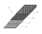
一方、次世代超電導テープとして、RE(希土類)系超電導薄膜(薄膜系)の開発が進められている(例えば特許文献1)。例えば図7に示すように、このRE系超電導薄膜11は、テープ状の金属補強板12上に順次中間層13、超電導薄膜14、保護層15を積層して形成される。具体例としては、例えば金属補強板12としてハステロイ(登録商標)、中間層13としてYSZ、超電導薄膜14としてY系123構造(YBa2Cu3Oy)薄膜、保護層15として銀が用いられている。通常、これら中間層13や超電導薄膜14はレーザ蒸着などにより金属補強板12の片面のみに形成される。このようなRE系超電導薄膜11は、厚みを薄く形成することができ、金属補強板12の存在によって引張力に対しては比較的に優れた強度を有している。このようなRE系超電導薄膜11を用いて3心一括型の超電導ケーブル10を形成する場合にもBi系超電導テープ21の場合と同様に構成される(図6参照)。
ところで、図6に示すような3心一括型の超電導ケーブル10に交流電流を流すと、超電導テープにおける微小な損失により僅かな熱が発生するため、温度上昇を抑えるための冷却が必要となる。交流損失が大きいと熱の発生も大きくなるため、大型の冷凍機を用意しなければならず、経済性が著しく損なわれる。超電導ケーブルの場合、導体周方向に磁場が形成されるため、超電導層(超電導導体層又は超電導シールド層)を形成する超電導テープの厚さを薄くする程、交流損失を低減することができる。従って、交流損失を低減するためには、テープ状に形成された個々の超電導テープ(Bi系超電導テープ21又はRE系超電導薄膜11)の厚みをできるだけ薄くすることが望ましい。
By the way, if an alternating current is passed through the three-conductor-type
しかし、現状のBi系超電導テープ製造設備では、超電導テープの厚さを薄くすると幅も縮小せざるを得ない。個々の超電導テープの厚さと幅を縮小しすぎると、超電導層を形成するために必要な超電導テープの本数が増加するため、超電導テープを繰り出すリールが多数必要となり、既存の設備では製造ができなくなる。また、機械的な強度が低下して必要強度を確保できなくなったり、超電導テープの本数の増加によって巻回時に個々の超電導テープの間隔を適切に確保するのが困難になり、もつれや乗り上げが発生したりする等の製作段階における問題が発生する。また、上述のような超電導ケーブルを直流用として用いる場合、大容量化を図るために、超電導テープの本数を増やすと、交流用の場合と同様に製作段階での問題が発生する。このようなことから、これらの問題を解決するための対策が求められていた。 However, in the current Bi-based superconducting tape manufacturing equipment, if the thickness of the superconducting tape is reduced, the width must be reduced. If the thickness and width of individual superconducting tapes are reduced too much, the number of superconducting tapes required to form the superconducting layer will increase, and a large number of reels will be required to feed the superconducting tapes, making it impossible to manufacture with existing equipment. . In addition, the required strength cannot be ensured due to a decrease in mechanical strength, or the increase in the number of superconducting tapes makes it difficult to properly secure the spacing between the individual superconducting tapes during winding, resulting in entanglement and climbing. Problems in the production stage occur. Further, when the superconducting cable as described above is used for direct current, if the number of superconducting tapes is increased in order to increase the capacity, problems at the production stage occur as in the case of alternating current. For this reason, a countermeasure for solving these problems has been demanded.
一方、薄膜系(RE系超電導薄膜11)では、電子レーザ等によるスリット加工が可能であるため、超電導テープを形成する際に幅の調整が容易である。もともと超電導薄膜14は数ナノの薄さなので電気的ロス(交流損失)は少ない。従って、超電導ケーブルの超電導層を形成するに際しては、超電導テープの幅をどの程度に設定すればよいかが課題となる。この点に関しては、Bi系超電導テープ21の場合と同様に、幅を縮小しすぎると、超電導テープを繰り出すリールが多数必要となり、既存の設備で対処できなくなる。また、幅の縮小によって超電導テープの本数が増え過ぎると、その巻回工程で、もつれたり、乗り上げたりするようなトラブルが発生することも懸念される。
On the other hand, in the thin film system (RE-based superconducting thin film 11), slit processing by an electron laser or the like is possible, so that the width can be easily adjusted when forming a superconducting tape. Originally, the superconducting
本発明は、このような事情に鑑みてなされ、超電導テープの厚みを薄くしても必要な機械的強度を確保できる超電導複合線材によって形成される超電導層を備えた超電導ケーブルを提供することを目的とする。 The present invention has been made in view of such circumstances, and an object of the present invention is to provide a superconducting cable including a superconducting layer formed of a superconducting composite wire that can ensure the required mechanical strength even if the thickness of the superconducting tape is reduced. And
本発明の超電導ケーブルは、フォーマの外周に、超電導複合線材が巻回されて形成される超電導層が、絶縁層を介して、複数層配設される超電導ケーブルであって、
前記超電導複合線材は、補強基板上に1本又は互いに並列に配列された複数本の超電導テープを一体化して形成され、かつ、内側に配設される超電導層を形成する前記超電導複合線材の幅が、外側に配設される超電導層を形成する前記超電導複合線材の幅よりも狭く設定されることを特徴とする。
The superconducting cable of the present invention is a superconducting cable in which a superconducting layer formed by winding a superconducting composite wire around the outer periphery of the former is disposed in a plurality of layers via an insulating layer,
The superconducting composite wire is formed by integrating a single superconducting tape or a plurality of superconducting tapes arranged in parallel with each other on a reinforcing substrate, and forms a superconducting layer disposed inside the superconducting composite wire. Is set to be narrower than the width of the superconducting composite wire forming the superconducting layer disposed on the outside.
超電導複合線材は、超電導テープを薄く形成しても補強基板によって、その強度が補強されるため、機械的強度を低下させることなく超電導テープの薄型化を達成することができる。また、複数本の超電導テープを一本化することができるので、超電導テープの薄型化を達成した上で超電導ケーブルの超電導層を形成するために必要な超電導複合線材の本数を少なくすることができる。従って、超電導ケーブルの製作段階における巻回工程で、超電導複合線材を繰り出すリールが少なくて済み、既存の設備に対応できるようになる。また、所要の機械的強度を確保できるため、製作段階における巻回工程で、超電導複合線材が破断したり、もつれたり、乗り上げたりするようなトラブルの発生を少なくすることができる。 Since the strength of the superconducting composite wire is reinforced by the reinforcing substrate even if the superconducting tape is thinly formed, the superconducting tape can be made thin without reducing the mechanical strength. In addition, since a plurality of superconducting tapes can be integrated, it is possible to reduce the number of superconducting composite wires necessary to form a superconducting layer of a superconducting cable while achieving a thin superconducting tape. . Therefore, in the winding process in the production stage of the superconducting cable, the number of reels for feeding the superconducting composite wire can be reduced, and the existing equipment can be handled. In addition, since the required mechanical strength can be ensured, it is possible to reduce the occurrence of troubles such as breakage, entanglement, and climbing of the superconducting composite wire during the winding process in the production stage.
このような超電導複合線材を交流用の超電導ケーブルに使用する場合には、径の小さい超電導導体層を形成する超電導複合線材の幅が、径の大きい超電導シールド層を形成する超電導複合線材の幅よりも狭く設定されるので、超電導導体層が多角形化することなく、整った円形状に形成することができるため、交流損失を低減することができる。また、超電導シールド層では、超電導複合線材の幅を広くしても多角形化せず厚みを薄く形成できるので、同層を形成するために必要な超電導複合線材の本数を少なくして交流損失を低減することができる。一方、直流用として大容量化を図る場合、より少ない本数の超電導複合線材によって大容量化を達成できるため、巻回工程で、超電導複合線材が破断したり、もつれたり、乗り上げたりするようなトラブルの発生を少なくすることができる。尚、超電導層は、交流用の超電導ケーブルでは超電導導体層と超電導シールド層、直流用の超電導ケーブルでは内側超電導層と外側超電導層が該当する。 When such a superconducting composite wire is used for a superconducting cable for alternating current, the width of the superconducting composite wire forming the superconducting conductor layer having a small diameter is larger than the width of the superconducting composite wire forming the superconducting shield layer having a large diameter. Since the superconducting conductor layer can be formed in a well-rounded shape without being polygonal, AC loss can be reduced. In addition, since the superconducting shield layer can be made thin without forming a polygon even if the width of the superconducting composite wire is widened, AC loss is reduced by reducing the number of superconducting composite wires necessary to form the same layer. Can be reduced. On the other hand, when increasing the capacity for direct current use, a larger capacity can be achieved with a smaller number of superconducting composite wires, so troubles such as the superconducting composite wires breaking, entangled, or climbing during the winding process. Can be reduced. The superconducting layer corresponds to a superconducting conductor layer and a superconducting shield layer in an AC superconducting cable, and an inner superconducting layer and an outer superconducting layer in a DC superconducting cable.
前記外側に配設される超電導層を形成する前記超電導複合線材の超電導テープの本数が、前記内側に配設される超電導層を形成する前記超電導複合線材の超電導テープの本数よりも多く設定されるようにしてもよい。このようにすれば、径の小さい内側の超電導層を形成する超電導複合線材では、超電導テープの本数を少なくすることによって、超電導複合線材の幅を狭くして、超電導層を多角形化することなく、整った円形状に形成することができる。また、径の大きな外側の超電導層を形成する超電導複合線材では、超電導テープの本数を多くして、必要な超電導複合線材の本数を少なくすることができる。これにより、超電導ケーブルの製作段階における巻回工程で、超電導複合線材を繰り出すリールが少なくて済み、既存の設備に対応できるようになる。 The number of superconducting tapes of the superconducting composite wire that forms the superconducting layer disposed on the outside is set to be greater than the number of superconducting tapes of the superconducting composite wire that forms the superconducting layer disposed on the inside. You may do it. In this way, in the superconducting composite wire that forms the inner superconducting layer with a small diameter, by reducing the number of superconducting tapes, the width of the superconducting composite wire is narrowed, and the superconducting layer is made polygonal. Can be formed into a well-rounded shape. Moreover, in the superconducting composite wire forming the outer superconducting layer having a large diameter, the number of superconducting tapes can be increased and the number of necessary superconducting composite wires can be reduced. As a result, in the winding process in the production stage of the superconducting cable, the number of reels for feeding the superconducting composite wire can be reduced, and the existing equipment can be handled.
前記超電導複合線材の幅が、前記超電導複合線材によって形成する超電導層の径に略比例して設定されるようにしてもよい。このような超電導ケーブルを交流用として使用する場合には、内側の径の小さい超電導導体層を多角形化させることなく、整った円形状に形成することができるため、交流損失を低減することができる。また、超電導シールド層では、超電導複合線材の幅を広くしても厚みを薄く形成できるので、同層を形成するために必要な超電導複合線材の本数を少なくして交流損失を低減することができる。一方、直流用として大容量化を図る場合、より少ない本数の超電導複合線材によって大容量化を達成できるため、巻回工程で、超電導複合線材が破断したり、もつれたり、乗り上げたりするようなトラブルの発生を少なくすることができる。また、超電導複合線材の幅を、超電導層の径に略比例して設定すれば、内側に形成される超電導層に必要な超電導複合線材の本数と、外側に形成される超電導層に必要な超電導複合線材の本数と、を一致させることができるため、超電導ケーブルの製作段階にて、内側と外側の超電導層を形成する超電導複合線材の繰り出し用のボビン数を同数に設定できる利点がある。 The width of the superconducting composite wire may be set substantially proportional to the diameter of the superconducting layer formed by the superconducting composite wire. When such a superconducting cable is used for alternating current, the superconducting conductor layer having a small inner diameter can be formed into a well-rounded shape without making it polygonal, thereby reducing alternating current loss. it can. In addition, since the thickness of the superconducting shield layer can be reduced even if the width of the superconducting composite wire is widened, the number of superconducting composite wires required to form the same layer can be reduced to reduce AC loss. . On the other hand, when increasing the capacity for direct current use, a larger capacity can be achieved with a smaller number of superconducting composite wires, so troubles such as the superconducting composite wires breaking, entangled, or climbing during the winding process. Can be reduced. In addition, if the width of the superconducting composite wire is set approximately in proportion to the diameter of the superconducting layer, the number of superconducting composite wires required for the superconducting layer formed on the inside and the superconducting power necessary for the superconducting layer formed on the outside Since the number of composite wires can be made to coincide with each other, there is an advantage that the number of bobbins for feeding the superconducting composite wire forming the inner and outer superconducting layers can be set to the same number in the superconducting cable manufacturing stage.
前記超電導テープは、テープ状に形成されたBi系超電導テープであるようにしてもよい。このBi系超電導テープは、例えばBi2223相からなる複数本の超電導フィラメントを銀などの安定化材中に埋設して薄膜状としたものを用いることができる。 The superconducting tape may be a Bi-based superconducting tape formed in a tape shape. As this Bi-based superconducting tape, for example, a thin film formed by embedding a plurality of Bi2223 superconducting filaments in a stabilizing material such as silver can be used.
前記超電導テープは、テープ状に形成されたRE系超電導薄膜であるようにしてもよい。このRE系超電導薄膜は、テープ状の金属補強板上に順次中間層、超電導薄膜、保護層を積層して形成される。例えば金属補強板としてハステロイ(登録商標)、中間層としてYSZ、超電導薄膜としてY系123構造(YBa2Cu3Oy)薄膜、保護層として銀が用いられたもの等を挙げることができる。尚、ハステロイ等からなる金属補強板を補強基板として用いてもよい。 The superconducting tape may be an RE-based superconducting thin film formed in a tape shape. This RE-based superconducting thin film is formed by sequentially laminating an intermediate layer, a superconducting thin film, and a protective layer on a tape-shaped metal reinforcing plate. For example, there may be mentioned those in which Hastelloy (registered trademark) is used as a metal reinforcing plate, YSZ is used as an intermediate layer, Y-type 123 (YBa 2 Cu 3 Oy) thin film is used as a superconducting thin film, and silver is used as a protective layer. In addition, you may use the metal reinforcement board which consists of Hastelloy etc. as a reinforcement board | substrate.
前記超電導層は、超電導導体層と、その外側に配設される超電導シールド層と、を備えるようにしてもよい。このように交流用の超電導ケーブルを構成する場合、径の小さい超電導導体層には幅の狭い超電導複合線材を用いることによって、超電導導体層を、多角形化させることなく整った円形状に形成することができる。一方、径の大きい超電導シールド層には厚みを増加させることなく幅を広くした超電導複合線材を用いることによって、径方向に高い密度で巻装して超電導層を形成することができる。このような構成により、交流損失を少なくすることができる。また、超電導層を形成する超電導複合線材繰り出し用のボビン数を減らすことができる。 The superconducting layer may include a superconducting conductor layer and a superconducting shield layer disposed outside the superconducting conductor layer. When a superconducting cable for alternating current is constructed in this way, the superconducting conductor layer is formed into a neat circular shape without making it polygonal by using a narrow superconducting composite wire for the superconducting conductor layer with a small diameter. be able to. On the other hand, by using a superconducting composite wire having a wide width without increasing the thickness, the superconducting layer can be formed by winding at a high density in the radial direction. With such a configuration, AC loss can be reduced. In addition, the number of bobbins for feeding a superconducting composite wire forming the superconducting layer can be reduced.
前記超電導層は、内側超電導層と、その外側に配設される外側超電導層と、を備えるようにしてもよい。このように直流用の超電導ケーブルを構成して大容量化を図ろうとする場合には、より少ない本数の超電導複合線材によって大容量化を達成できるため、巻回工程で、超電導複合線材が破断したり、もつれたり、乗り上げたりするようなトラブルの発生を少なくすることができる。 The superconducting layer may include an inner superconducting layer and an outer superconducting layer disposed on the outer side. When a DC superconducting cable is constructed in this way to increase the capacity, the capacity can be increased with a smaller number of superconducting composite wires, so the superconducting composite wire breaks during the winding process. It is possible to reduce the occurrence of troubles such as entanglement, entanglement, and riding.
本発明の超電導ケーブルは、内側に配設される超電導層を形成する超電導複合線材の幅を、外側に配設される超電導層を形成する超電導複合線材の幅よりも狭く設定するので、内側の超電導層を多角形化させることなく整った円形状に形成することができるため、交流用として用いる場合、交流損失を低減することができる。また、径の大きい超電導シールド層には厚みを増加させることなく幅を広くした超電導複合線材を用いることによって、径方向に高い密度で巻装して超電導層を形成することができることによっても、交流損失を少なくすることができる。一方、直流用として大容量化を図る場合、より少ない本数の超電導複合線材によって大容量化を達成できるため、巻回工程で、超電導複合線材が破断したり、もつれたり、乗り上げたりするようなトラブルの発生を少なくすることができる。 In the superconducting cable of the present invention, the width of the superconducting composite wire that forms the superconducting layer disposed inside is set narrower than the width of the superconducting composite wire that forms the superconducting layer disposed outside. Since the superconducting layer can be formed in a well-rounded shape without making it polygonal, AC loss can be reduced when used for AC. In addition, by using a superconducting composite wire with a wide width without increasing the thickness for the superconducting shield layer with a large diameter, the superconducting layer can be formed by being wound at a high density in the radial direction. Loss can be reduced. On the other hand, when increasing the capacity for direct current use, a larger capacity can be achieved with a smaller number of superconducting composite wires, so troubles such as the superconducting composite wires breaking, entangled, or climbing during the winding process. Can be reduced.
以下に、本発明の実施の形態に係る超電導複合線材について図面を参照しつつ詳細に説明する。 Hereinafter, a superconducting composite wire according to an embodiment of the present invention will be described in detail with reference to the drawings.
図1(a)は交流用の超電導ケーブル20のケーブルコア29の断面図、(b)は、超電導導体層22を形成する超電導複合線材S1の断面図、(c)は、超電導シールド層24を形成する超電導複合線材S2の断面図、(d)は、超電導ケーブル20の断面図である。図2(a)は、超電導複合線材Sの一例を示す断面図、(b)は別の例を示す断面図である。図3(a)〜(c)は、超電導複合線材Sのその他の例を示す断面図である。この超電導ケーブル20は、まず、図1(d)に示すように、フォーマFを中心として、その外周に、クッション層Cと、超電導複合線材Sが巻回されて形成される超電導導体層22と、クラフト紙やクラフト紙とポリオレフィンフィルムをラミネートした複合紙等からなる絶縁層23と、超電導複合線材Sが巻回されて形成される超電導シールド層24と、を備えたケーブルコア29が形成される。そして、3本のケーブルコア29が互いに撚り合わされて内管26と外管27とで形成される二重断熱管内に挿入され、内管26内に冷媒流通路25が形成される。その外管27は防食層28によって覆われ、内管26と外管27の間は真空引きされて真空層とされる。
1 (a) is a cross-sectional view of a
このように構成される超電導ケーブル20にあって、その超電導導体層22と超電導シールド層24を形成する超電導複合線材S(S1,S2)は、例えば図2(a)(b)に示すように、補強基板32に超電導テープ31を一体化して形成される。図2(a)に示す例では、例えば1本のBi系超電導テープからなる超電導テープ31の両面に補強基板32,32を半田接合等によって一体化して構成される。また、図2(b)に示す例では、例えば互いに並列に配列された2本のBi系超電導テープからなる超電導テープ31,31の両面に補強基板32,32を半田接合等によって一体化して構成される。補強基板32は、例えば銅やその合金、ステンレス等で形成することができる。このような補強基板32を用いることによって、所要の機械的強度(引張り強度及び曲げ強度)と充分な可撓性を備えた超電導複合線材Sを形成することができる。また、補強基板32の素材としては、このような導電性の金属材だけでなく、絶縁性と耐熱性に優れたポリイミドテープ等を用いることもできる。尚、超電導テープ31としてRE系超電導薄膜を用いる場合には、例えばハステロイ(登録商標)からなる金属補強板を所要厚さに設定して補強基板32として用いてもよい。
In the
このように構成される超電導複合線材Sは、超電導テープ31を薄く形成しても補強基板32によって、その強度が補強されるため、機械的強度を低下させることなく超電導テープ31の薄型化を達成することができる。また、複数本の超電導テープ31を一本化することができるので、超電導テープ31の薄型化を達成した上で超電導ケーブル20の超電導層(超電導導体層22及び超電導シールド層24)を形成するために必要な超電導複合線材Sの本数を少なくすることができる。従って、製作段階における巻回工程で、超電導複合線材Sを繰り出すリールが少なくて済み、既存の設備に対応できるようになる。また、所要の機械的強度を確保できるため、製作段階における巻回工程で、超電導複合線材Sが破断したり、もつれたり、乗り上げたりするようなトラブルの発生を少なくすることができる。そして、図2(a)(b)に示すように、超電導複合テープ31が補強基板32によって挟まれるため、超電導ケーブル20の製作段階等において超電導複合テープ31を保護することができる。尚、図示のように、補強基板32の幅は、超電導テープ31の全幅よりも若干大に設定すれば、超電導テープ31をより効果的に保護することができる。また、その補強基板32の外側端縁eを、面取り状に形成すれば、超電導導体層22の上に絶縁層23を形成する際に、絶縁テープが破損するのを回避することができる。
The superconducting composite wire S configured as described above is thinned without increasing the mechanical strength because the strength is reinforced by the reinforcing
そして、その超電導複合線材Sの幅b1,b2は、図1(b)(c)に示すように、超電導層22,24の径r1,r2に略比例した値に設定するのが好ましい。例えば超電導導体層22の半径r1と超電導シールド層24の半径r2の比率が1/2の場合、超電導複合線材S1,S2の幅b1,b2の比率も1/2に設定する。尚、超電導複合線材S1,S2の幅b1,b2が異なっても厚さtは同じである。この場合、超電導複合線材S1,S2を構成する超電導テープ31の本数をn1,n2とすれば、2πr1/n1=2πr2/n2・・・(1)式が満たされるのが好ましい。従って、r2=2r1の場合、(1)式から、n2=2n1となり、超電導導体層22を形成する超電導複合線材S1は、例えば図2(a)に示すような1本の超電導テープ31を補強基板32で補強した構成として、外側の超電導シールド層24を形成する超電導複合線材S2は、例えば図2(b)に示すような2本の超電導テープ31,31を補強基板32で補強した構成とすることができる。これにより、超電導導体層22と、超電導シールド層24とで、超電導複合線材Sの必要本数を同数にすることができるため、超電導ケーブル20の製作段階における超電導複合線材Sの巻回工程での作業性が良好になる。ちなみに、図2(a)(b)に示す超電導複合線材Sでは、例えば、超電導テープ31の幅2.6mm、厚さ0.18mm、超電導複合線材S1の補強基板32の幅b1=2.7mm、厚さt=20〜100μm、超電導複合線材S2の補強基板32の幅b2=5.3mm、厚さ=20〜100μmに設定することができる。
Then, the widths b 1 and b 2 of the superconducting composite wire S are set to values substantially proportional to the diameters r 1 and r 2 of the
このように超電導複合線材Sの幅を選択することによって、内側の超電導導体層22を多角形化することなく整った円形状に形成することができ、交流損失を低減することができる。また、図2(b)に示すように、2本の超電導テープ31,31を一体化しても、超電導複合線材S2の厚みは増加することはないので、超電導シールド層24を形成するために必要な超電導複合線材Sの本数を少なくして交流損失を低減することができる。尚、超電導層22(24)が、多角形化すると、径方向に形成される磁場が拡大するため交流損失が増加する。一方、このような超電導複合線材Sで直流用の超電導ケーブル20を形成して大容量化を図る場合には、より少ない本数の超電導複合線材Sによって大容量化を達成できるため、その製作段階での超電導複合線材Sの巻回工程で、超電導複合線材Sが破断したり、もつれたり、乗り上げたりするようなトラブルの発生を少なくすることができる。尚、直流用の超電導ケーブル20では内側超電導層22と外側超電導層24が超電導層に該当する。
By selecting the width of the superconducting composite wire S in this way, the inner
超電導複合線材Sを構成する超電導テープ31の幅は、1.5〜4.5mmに設定することができ、1〜5本の超電導テープ31を補強基板32に一体化することができる。その補強基板32の幅は、2〜10mmに設定することができる。この程度の幅であれば、例えば銅やその合金、ステンレス等を素材として必要な機械的強度と充分な可撓性を確保することができる。また、これらの導電体を用いることによって、短絡電流が発生した場合には、補強基板32に短絡電流を流すことで、超電導テープ31を保護することができる。尚、補強基板32の幅が2mm未満になると、超電導複合線材Sが所要の機械的強度を確保するのが難しくなり、また、捩れやすくなる。10mmを超えると、超電導複合線材Sを巻回して超電導層を形成した際に、その外形が多角形化しやすくなり、特に、内側超電導層では、円形に近い形状に整えるのが難しくなる。
The width of the
超電導複合線材Sは、例えば図3(a)(b)に示すように、超電導テープ31の片面にのみ補強基板32を一体化させてもよい。このように、超電導テープ31を補強基板32の片面にのみ形成した超電導複合線材Sで、超電導層を形成する場合、超電導テープ31が形成されている側を外側にして巻回すれば、超電導ケーブルの接続部において、接続部材を超電導層に直接接続できるため、接続抵抗を低減できる利点がある。また、図3(b)(c)に示す例では、補強基板32に、超電導テープ31の幅方向への移動を抑制するための規制部32aを形成している。このような規制部32aは、例えば長手方向に所定間隔おきの突起状等に形成してもよく、長手方向に連続した突出状に形成してもよい。このような規制部32aを形成することによって、複数本の超電導テープ31を補強基板32に一体化する工程から、超電導層を形成するためにフォーマ(又は絶縁層)に超電導複合線材Sを巻回する工程、ケーブルコアの撚り合わせ工程、を経て使用段階に至る間において、超電導テープ31と補強基板32とが種々の外力や熱の影響を受けても、超電導テープ31を補強基板32に対して安定した整列状態に保持することができる。尚、図3(c)に示す例では、上下の補強基板32に規制部32aを形成しているが、片方の補強基板32のみに規制部32aを形成してもよい。尚、本発明は、実施の形態に限定されることなく、発明の要旨を逸脱しない限りにおいて、適宜、必要に応じて改良、変更等は自由である。
In the superconducting composite wire S, for example, as shown in FIGS. 3A and 3B, the reinforcing
本発明の超電導ケーブルは、交流損失の低減化を図れるため、長距離大容量の交流送電用に好適に採用することができる。 Since the superconducting cable of the present invention can reduce AC loss, it can be suitably used for long-distance and large-capacity AC power transmission.
1 フォーマ 2 超電導層(超電導導体層) 3 絶縁層
4 超電導層(超電導シールド層) 5 冷媒流通路 6 内管 7 外管
8 防食層 9 ケーブルコア 10 超電導ケーブル
11 RE系超電導薄膜 12 金属補強板 13 中間層
14 超電導薄膜 15 保護層 16 層間絶縁 17 層間絶縁
18 外層 20 超電導ケーブル 21 Bi系超電導テープ
21a 金属シース 21b 超電導フィラメント
22 超電導層(超電導導体層) 23 絶縁層
24 超電導層(超電導シールド層) 25 冷媒流通路 26 内管
27 外管 28 防食層 29 ケーブルコア F フォーマ
S,S1,S2 超電導複合線材 e 外側端縁 C クッション層
31 超電導テープ 32 補強基板 32a 規制部
DESCRIPTION OF
Claims (7)
前記超電導複合線材は、1本又は互いに並列に配列された複数本の超電導テープの両面に、銅やその合金、ステンレス等の導電体の金属材から構成される補強基板を一体化して形成され、かつ、
内側に配設される超電導層を形成する前記超電導複合線材の幅が、外側に配設される超電導層を形成する前記超電導複合線材の幅よりも狭く設定されることを特徴とする超電導ケーブル。 A superconducting layer formed by winding a superconducting composite wire around the outer periphery of the former is a superconducting cable provided with a plurality of layers via an insulating layer,
The superconducting composite wire is on both sides of one or a plurality of superconducting tapes arranged in parallel with each other, are integrally formed of copper or an alloy, the reinforcing substrate composed of a metal material conductor such as stainless steel, And,
A superconducting cable, characterized in that a width of the superconducting composite wire forming the superconducting layer disposed inside is set narrower than a width of the superconducting composite wire forming the superconducting layer disposed outside.
Priority Applications (1)
| Application Number | Priority Date | Filing Date | Title |
|---|---|---|---|
| JP2007211069A JP4986291B2 (en) | 2007-08-13 | 2007-08-13 | Superconducting cable |
Applications Claiming Priority (1)
| Application Number | Priority Date | Filing Date | Title |
|---|---|---|---|
| JP2007211069A JP4986291B2 (en) | 2007-08-13 | 2007-08-13 | Superconducting cable |
Publications (2)
| Publication Number | Publication Date |
|---|---|
| JP2009048792A JP2009048792A (en) | 2009-03-05 |
| JP4986291B2 true JP4986291B2 (en) | 2012-07-25 |
Family
ID=40500842
Family Applications (1)
| Application Number | Title | Priority Date | Filing Date |
|---|---|---|---|
| JP2007211069A Expired - Fee Related JP4986291B2 (en) | 2007-08-13 | 2007-08-13 | Superconducting cable |
Country Status (1)
| Country | Link |
|---|---|
| JP (1) | JP4986291B2 (en) |
Families Citing this family (3)
| Publication number | Priority date | Publication date | Assignee | Title |
|---|---|---|---|---|
| JP5041414B2 (en) * | 2007-10-26 | 2012-10-03 | 古河電気工業株式会社 | Superconducting wire and superconducting conductor |
| US10096403B2 (en) | 2013-03-15 | 2018-10-09 | Furukawa Electric Co., Ltd. | Method for producing superconductive conductor and superconductive conductor |
| JP6522891B2 (en) * | 2014-05-23 | 2019-05-29 | 株式会社東芝 | Superconducting tape wire and superconducting coil |
Family Cites Families (4)
| Publication number | Priority date | Publication date | Assignee | Title |
|---|---|---|---|---|
| JPH0745136A (en) * | 1993-07-30 | 1995-02-14 | Furukawa Electric Co Ltd:The | Oxide superconductor |
| JPH0773757A (en) * | 1993-09-03 | 1995-03-17 | Furukawa Electric Co Ltd:The | Manufacture of oxide superconductor |
| JPH09237529A (en) * | 1996-02-27 | 1997-09-09 | Furukawa Electric Co Ltd:The | High temperature superconductive cable conductor and manufacture thereof |
| JP5115778B2 (en) * | 2006-01-16 | 2013-01-09 | 住友電気工業株式会社 | Superconducting cable |
-
2007
- 2007-08-13 JP JP2007211069A patent/JP4986291B2/en not_active Expired - Fee Related
Also Published As
| Publication number | Publication date |
|---|---|
| JP2009048792A (en) | 2009-03-05 |
Similar Documents
| Publication | Publication Date | Title |
|---|---|---|
| JP6080168B2 (en) | Intermediate connection of superconducting cable | |
| JP2007287388A (en) | Superconductive cable core, and superconductive cable | |
| JP5192741B2 (en) | Superconducting conductor and superconducting cable with superconducting conductor | |
| US20080312089A1 (en) | Superconducting Cable | |
| JP5416509B2 (en) | Intermediate connection structure of superconducting cable | |
| US8260386B2 (en) | Armored superconducting winding and method for its production | |
| WO2007080794A1 (en) | Superconducting cable | |
| JP4986291B2 (en) | Superconducting cable | |
| JP7074190B2 (en) | Superconducting wire, laminated superconducting wire, superconducting coil and superconducting cable | |
| WO2007122670A1 (en) | Superconducting cable | |
| JP6548916B2 (en) | High temperature superconducting coil | |
| JP5397994B2 (en) | Superconducting cable | |
| JP5936130B2 (en) | Superconducting cable and bus bar | |
| JP2008053215A (en) | Superconducting wire rod, superconductor, and superconductive cable | |
| JP2009048793A (en) | Superconducting compound wire rod and superconducting cable | |
| JP5829634B2 (en) | Superconducting cable terminal structure | |
| JP4978397B2 (en) | Superconducting cable | |
| JP6163039B2 (en) | Superconducting cable | |
| JP4662203B2 (en) | Superconducting cable | |
| JP4566576B2 (en) | Dislocation segment conductor | |
| JP5041414B2 (en) | Superconducting wire and superconducting conductor | |
| JP2004063225A (en) | Dislocation superconductivity tape unit and superconductive cable | |
| JP5771509B2 (en) | Superconducting cable | |
| JP2012174669A (en) | Normal temperature insulating type superconducting cable | |
| JP2001256841A (en) | Superconductive cable and magnet using the same |
Legal Events
| Date | Code | Title | Description |
|---|---|---|---|
| A711 | Notification of change in applicant |
Free format text: JAPANESE INTERMEDIATE CODE: A711 Effective date: 20090206 |
|
| A621 | Written request for application examination |
Free format text: JAPANESE INTERMEDIATE CODE: A621 Effective date: 20100317 |
|
| A977 | Report on retrieval |
Free format text: JAPANESE INTERMEDIATE CODE: A971007 Effective date: 20120126 |
|
| A131 | Notification of reasons for refusal |
Free format text: JAPANESE INTERMEDIATE CODE: A131 Effective date: 20120131 |
|
| A521 | Written amendment |
Free format text: JAPANESE INTERMEDIATE CODE: A523 Effective date: 20120328 |
|
| TRDD | Decision of grant or rejection written | ||
| A01 | Written decision to grant a patent or to grant a registration (utility model) |
Free format text: JAPANESE INTERMEDIATE CODE: A01 Effective date: 20120419 |
|
| A01 | Written decision to grant a patent or to grant a registration (utility model) |
Free format text: JAPANESE INTERMEDIATE CODE: A01 |
|
| A61 | First payment of annual fees (during grant procedure) |
Free format text: JAPANESE INTERMEDIATE CODE: A61 Effective date: 20120423 |
|
| R150 | Certificate of patent or registration of utility model |
Ref document number: 4986291 Country of ref document: JP Free format text: JAPANESE INTERMEDIATE CODE: R150 Free format text: JAPANESE INTERMEDIATE CODE: R150 |
|
| FPAY | Renewal fee payment (event date is renewal date of database) |
Free format text: PAYMENT UNTIL: 20150511 Year of fee payment: 3 |
|
| R250 | Receipt of annual fees |
Free format text: JAPANESE INTERMEDIATE CODE: R250 |
|
| R250 | Receipt of annual fees |
Free format text: JAPANESE INTERMEDIATE CODE: R250 |
|
| S533 | Written request for registration of change of name |
Free format text: JAPANESE INTERMEDIATE CODE: R313533 |
|
| R350 | Written notification of registration of transfer |
Free format text: JAPANESE INTERMEDIATE CODE: R350 |
|
| R250 | Receipt of annual fees |
Free format text: JAPANESE INTERMEDIATE CODE: R250 |
|
| R250 | Receipt of annual fees |
Free format text: JAPANESE INTERMEDIATE CODE: R250 |
|
| R250 | Receipt of annual fees |
Free format text: JAPANESE INTERMEDIATE CODE: R250 |
|
| LAPS | Cancellation because of no payment of annual fees |