JP4982598B2 - Wireless power transmission system, power transmission device and power reception device of the system - Google Patents
Wireless power transmission system, power transmission device and power reception device of the system Download PDFInfo
- Publication number
- JP4982598B2 JP4982598B2 JP2010199492A JP2010199492A JP4982598B2 JP 4982598 B2 JP4982598 B2 JP 4982598B2 JP 2010199492 A JP2010199492 A JP 2010199492A JP 2010199492 A JP2010199492 A JP 2010199492A JP 4982598 B2 JP4982598 B2 JP 4982598B2
- Authority
- JP
- Japan
- Prior art keywords
- power
- authentication
- power transmission
- resonator
- transmission
- Prior art date
- Legal status (The legal status is an assumption and is not a legal conclusion. Google has not performed a legal analysis and makes no representation as to the accuracy of the status listed.)
- Expired - Fee Related
Links
- 230000005540 biological transmission Effects 0.000 title claims description 210
- 238000004891 communication Methods 0.000 claims description 111
- 238000001514 detection method Methods 0.000 claims description 33
- 239000003990 capacitor Substances 0.000 claims description 20
- 239000011347 resin Substances 0.000 claims description 7
- 229920005989 resin Polymers 0.000 claims description 7
- 230000000630 rising effect Effects 0.000 claims description 6
- 238000012790 confirmation Methods 0.000 claims description 3
- 238000012544 monitoring process Methods 0.000 claims 1
- 238000010586 diagram Methods 0.000 description 14
- 238000000034 method Methods 0.000 description 11
- 230000001360 synchronised effect Effects 0.000 description 9
- 238000002474 experimental method Methods 0.000 description 4
- 230000004044 response Effects 0.000 description 4
- 230000010355 oscillation Effects 0.000 description 3
- 230000007704 transition Effects 0.000 description 3
- 238000006243 chemical reaction Methods 0.000 description 2
- 230000008878 coupling Effects 0.000 description 2
- 238000010168 coupling process Methods 0.000 description 2
- 238000005859 coupling reaction Methods 0.000 description 2
- 230000005674 electromagnetic induction Effects 0.000 description 2
- 230000008054 signal transmission Effects 0.000 description 2
- 241000272194 Ciconiiformes Species 0.000 description 1
- 101100172132 Mus musculus Eif3a gene Proteins 0.000 description 1
- 230000002457 bidirectional effect Effects 0.000 description 1
- 230000008859 change Effects 0.000 description 1
- 230000000694 effects Effects 0.000 description 1
- 238000005516 engineering process Methods 0.000 description 1
- 239000011521 glass Substances 0.000 description 1
- 238000012986 modification Methods 0.000 description 1
- 230000004048 modification Effects 0.000 description 1
- 230000008569 process Effects 0.000 description 1
- 238000012545 processing Methods 0.000 description 1
- 239000004065 semiconductor Substances 0.000 description 1
Images


Classifications
-
- H—ELECTRICITY
- H02—GENERATION; CONVERSION OR DISTRIBUTION OF ELECTRIC POWER
- H02J—CIRCUIT ARRANGEMENTS OR SYSTEMS FOR SUPPLYING OR DISTRIBUTING ELECTRIC POWER; SYSTEMS FOR STORING ELECTRIC ENERGY
- H02J50/00—Circuit arrangements or systems for wireless supply or distribution of electric power
- H02J50/10—Circuit arrangements or systems for wireless supply or distribution of electric power using inductive coupling
- H02J50/12—Circuit arrangements or systems for wireless supply or distribution of electric power using inductive coupling of the resonant type
-
- H—ELECTRICITY
- H02—GENERATION; CONVERSION OR DISTRIBUTION OF ELECTRIC POWER
- H02J—CIRCUIT ARRANGEMENTS OR SYSTEMS FOR SUPPLYING OR DISTRIBUTING ELECTRIC POWER; SYSTEMS FOR STORING ELECTRIC ENERGY
- H02J50/00—Circuit arrangements or systems for wireless supply or distribution of electric power
- H02J50/80—Circuit arrangements or systems for wireless supply or distribution of electric power involving the exchange of data, concerning supply or distribution of electric power, between transmitting devices and receiving devices
-
- H—ELECTRICITY
- H02—GENERATION; CONVERSION OR DISTRIBUTION OF ELECTRIC POWER
- H02J—CIRCUIT ARRANGEMENTS OR SYSTEMS FOR SUPPLYING OR DISTRIBUTING ELECTRIC POWER; SYSTEMS FOR STORING ELECTRIC ENERGY
- H02J7/00—Circuit arrangements for charging or depolarising batteries or for supplying loads from batteries
Landscapes
- Engineering & Computer Science (AREA)
- Computer Networks & Wireless Communication (AREA)
- Power Engineering (AREA)
- Near-Field Transmission Systems (AREA)
Description
本発明の実施形態は、同一周波数帯域での無線電力伝送と通信の共存が可能な無線電力伝送システム、該システムの送電装置および受電装置に関する。 Embodiments described herein relate generally to a wireless power transmission system capable of coexistence of wireless power transmission and communication in the same frequency band, and a power transmission device and a power reception device of the system.
無線電力伝送方式は、大別して電磁誘導型、電波受信型、磁場共鳴型がある。
電磁誘導型は、電動歯ブラシ、電動シェーバでの充電のために既に実用化されているものであり、効率も良いが、位置ずれに弱いために、送電部と受電部は概ね密着状態で配置し、それぞれ専用の送電部に受電部をしっかりとはめ込む形で用いられる。
Wireless power transmission systems are roughly classified into electromagnetic induction type, radio wave reception type, and magnetic field resonance type.
The electromagnetic induction type has already been put into practical use for charging with an electric toothbrush or electric shaver, and is efficient, but it is vulnerable to misalignment, so the power transmission unit and the power reception unit are arranged in close contact. The power receiving unit is securely fitted to each dedicated power transmission unit.
電波受信型は、ピッツバーグ動物園のペンギン舎等で実用にされていて、電力を電磁波として飛ばし、受電側ではそれを受信して電力に変換するものである。電磁誘導型の「送電部と受電部をほぼ密着させる」という制約は無くなるが、エネルギーの利用効率は、例えば900MHzで2m離れた状態で、ダイポールアンテナを使った場合、1%未満と非常に低いものになってしまう。そのため、送電部と受電部を十分隔離する必要があり、かつ消費電力は非常に低いアプリケーションに限定されていた。 The radio wave reception type is put into practical use in a penguin building of the Pittsburgh zoo, etc., where electric power is skipped as electromagnetic waves, and the power receiving side receives it and converts it into electric power. Although there is no restriction of electromagnetic induction-type “power transmitter and power receiver are almost in close contact”, the energy utilization efficiency is very low, for example, less than 1% when a dipole antenna is used with a distance of 2 m at 900 MHz. It becomes a thing. Therefore, it is necessary to sufficiently isolate the power transmission unit and the power reception unit, and power consumption is limited to very low applications.
磁場共鳴型(磁気共鳴型とも呼ぶ)は、これら先行方式の問題点をある程度克服するものとして、2007年にマサチューセッツ工業大学の研究者らによって実証されたもので、2mの距離で60Wの電球に約50%の効率で電力供給し、点灯させることに成功した。この方式は送電部、受電部それぞれに、特定周波数で共振する「共鳴器」を配して、その周波数での交流磁界を効率良く送受電部の近傍に集中させるのが特徴である。その結果として、将来的にはトロリー電車への給電等、大電力供給の応用にも道が開かれている。効率の良い伝送をするためには、共鳴器のQ値が高いことが条件となるのが特徴でもある。 The magnetic field resonance type (also called magnetic resonance type) was proved by researchers at the Massachusetts Institute of Technology in 2007 as a way to overcome these problems of the previous method to a 60 W bulb at a distance of 2 m. We succeeded in supplying power with about 50% efficiency and lighting. This method is characterized in that a “resonator” that resonates at a specific frequency is provided in each of the power transmission unit and the power reception unit, and an AC magnetic field at that frequency is efficiently concentrated in the vicinity of the power transmission / reception unit. As a result, in the future, there is a way to apply high power supply such as power supply to trolley trains. In order to perform efficient transmission, a high Q value of the resonator is a condition.
これらの技術を用いた無線電力伝送システムを実用化するためには、送電部・受電部間での認証、所要電力の申告等、何らかの通信機能が必須となる。 In order to put a wireless power transmission system using these technologies into practical use, some kind of communication function such as authentication between a power transmission unit and a power reception unit, declaration of required power, and the like is essential.
電力の伝送距離、効率、伝送電力の大きさ等の点で大きな可能性を持つ磁場共鳴型の無線電力伝送において、送受間の電力伝送およびデータ通信を最小の構成で効率よく行う無線電力伝送が望まれる。 In magnetic field resonance type wireless power transmission that has great potential in terms of power transmission distance, efficiency, transmission power, etc., wireless power transmission that efficiently performs power transmission and data communication between transmission and reception with minimal configuration desired.
磁場共鳴型の無線電力伝送において、送受間の電力伝送およびデータ通信を最小の構成で効率よく行う無線電力伝送システム、該システムの送電装置および受電装置を提供することを目的とする。 An object of the present invention is to provide a wireless power transmission system that efficiently performs power transmission and data communication between transmission and reception in a magnetic resonance type wireless power transmission with a minimum configuration, and a power transmission device and a power reception device of the system.
上記目的を達成するために、本発明の実施形態の無線電力伝送システムは、送電装置と受電装置との間で磁場共鳴による電力伝送と信号通信とを時分割で行なう無線電力伝送システムであって、前記送電装置は、所定の共振周波数で共振し、該共振のQ値を高低に切り換える第1の共振器と、前記信号通信を行うときに前記第1の共振器のQ値を低く設定し、前記電力伝送を行うときに前記第1の共振器のQ値を高く設定し、認証不要電力と認証電力とを含む電力を伝送し、該認証不要電力を所定の周期で伝送し、前記信号通信によって、認証され且つ割当期間が確認された受電装置に前記認証電力を伝送する第1の制御手段とを有し、前記受電装置は、前記所定の共振周波数で共振し、該共振のQ値を高低に切り換える第2の共振器と、前記信号通信を行うときに前記第2の共振器のQ値を低く設定し、前記電力伝送によって電力を受電するときに前記第2の共振器のQ値を高く設定し、前記認証不要電力を認証なしで受信し、前記認証電力を前記信号通信による認証および割当期間確認後に受電する第2の制御手段とを有することを特徴とする。
In order to achieve the above object, a wireless power transmission system according to an embodiment of the present invention is a wireless power transmission system that performs power transmission by magnetic resonance and signal communication in a time-sharing manner between a power transmission device and a power reception device. the power transmission device resonates at a predetermined resonant frequency, co the first resonator to switch to high and low Q value of vibration, the first set lower the Q value of the resonator when performing the signal communication A high Q value of the first resonator when performing the power transmission, transmitting power including authentication unnecessary power and authentication power, transmitting the authentication unnecessary power at a predetermined period, And a first control unit that transmits the authentication power to a power receiving apparatus that has been authenticated and whose allocation period has been confirmed by communication, wherein the power receiving apparatus resonates at the predetermined resonance frequency, and the Q value of the resonance a second resonator for switching the high and low of the previous Set lower the Q value of the second resonator when performing signal communication, the high setting the Q value of the second resonator when receiving power by the power transmission, authenticating the authentication unnecessary power And second control means for receiving the authentication power after receiving authentication and allocation period confirmation by the signal communication .
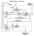
図1は、本発明の実施例に係る無線電力伝送システム300のブロック図である。無線電力伝送システム300は、送電装置100と受電装置200により構成される。受電装置200は複数あってもよい。
FIG. 1 is a block diagram of a wireless power transmission system 300 according to an embodiment of the present invention. The wireless power transmission system 300 includes a
[電力伝送および通信の概要]
まず、送電装置100と受電装置200間のワイヤレスの電力伝送および通信の概要について説明する。
送電装置100の共鳴器7(第1の共鳴器)の共振周波数と、受電装置200の共鳴器27(第2の共鳴器)の共振周波数とは同じに調整されており、一方の共鳴器を共振周波数で駆動して交流磁界を発生し、この交流磁界を介して他方の共鳴器が磁場共鳴することによって、ワイヤレスで電力および通信信号が伝送される。
[Outline of power transmission and communication]
First, an outline of wireless power transmission and communication between the
The resonance frequency of the resonator 7 (first resonator) of the
電力伝送については、送電装置100のループアンテナ6を高周波電力で駆動し、その発生する交流磁界に対して、送電装置100の共鳴器7と受電装置200の共鳴器27が磁場共鳴してその交流磁界を導き、ループアンテナ26にてその電力を捕捉することにより、送電装置100から受電装置200へワイヤレスで電力が伝送される。大きな電力の電力伝送を行うために、双方の共鳴器の共振のQ値(Quality Factor)は、高いQ値に設定される。例えば、共振周波数=20MHz、Q=1000とすると、マイナス3dBの帯域幅は、20MHz/1000=20kHzの狭い急峻な高効率の特性となる。
For power transmission, the
通信信号の伝送については、双方向であり、一方のループアンテナを通信信号で駆動し、その交流磁界を他方のループアンテナで捕捉することにより、ワイヤレスで通信信号が伝送される。通信信号は、その搬送波は共鳴器の共振周波数と同じ周波数であり、それを中心に変調されて帯域幅を有する信号である。高速のビットレートのデータ通信を行うために、双方の共鳴器の共振のQ値は低いQ値に設定される。これが高いQ値だと帯域幅が狭くて高速のデータ通信が行えないからである。低いQ値として、例えば、共振周波数=20MHz、Q=10とすると、マイナス3dBの帯域幅は、20MHz/10=2MHzのなだらかな特性となる。 The transmission of the communication signal is bidirectional, and the communication signal is transmitted wirelessly by driving one loop antenna with the communication signal and capturing the AC magnetic field with the other loop antenna. The communication signal is a signal having a bandwidth in which the carrier wave has the same frequency as the resonance frequency of the resonator and is modulated around it. In order to perform high-speed bit rate data communication, the resonance Q value of both resonators is set to a low Q value. This is because if the Q value is high, the bandwidth is narrow and high-speed data communication cannot be performed. As a low Q value, for example, when the resonance frequency is 20 MHz and Q = 10, the minus 3 dB bandwidth has a gentle characteristic of 20 MHz / 10 = 2 MHz.
データ通信時にこの低いQ値に設定され、データ通信の変調方式としてQPSKを用いれば、4Mb/s程度のデータ通信が可能となる。変調方式として高効率変調やパーシャルレスポンス、プリ等化等の技術を用いれば、更に高いビットレートが可能である。 If this low Q value is set at the time of data communication and QPSK is used as a modulation method for data communication, data communication of about 4 Mb / s becomes possible. If a technique such as high-efficiency modulation, partial response, or pre-equalization is used as the modulation method, a higher bit rate is possible.
電力伝送時と通信信号伝送時とでQ値を変えるので、送電装置100と受電装置200間で同期を取ってタイミングを制御して時分割で電力伝送と通信信号伝送を行い、その制御は、送電装置100の制御回路9(第1の制御手段)、受電装置200の制御回路29(第2の制御手段)により同期を取って行う。
Since the Q value is changed between power transmission and communication signal transmission, the
以下、各装置の構成および動作の詳細について説明する。
[送電装置100]
送電装置100は、発振器1、増幅器2、インピーダンス整合回路3、スイッチ4、バラン回路5(平衡不平衡変換)、ループアンテナ6、共鳴器7(第1の共鳴器)、通信回路8、制御回路9等により構成される。
Hereinafter, the configuration and operation of each device will be described in detail.
[Power transmission device 100]
The
発振器1、増幅器2、インピーダンス整合回路3は、電力伝送の専用部分である。発振器1は、所定の周波数の高周波信号を出力する。増幅器2は、それを所定のレベルまで増幅する。インピーダンス整合回路3は、アンテナ系との整合を取る回路である。
The
通信回路8は、データ変調/復調を行う通信専用部分である。電力伝送用の発振器1等と通信用の通信回路8とは、制御回路9の切換信号によりスイッチ4で時分割して切り換えられてバラン回路5につながる。
The communication circuit 8 is a communication-dedicated part that performs data modulation / demodulation. The
バラン回路5、ループアンテナ6、共鳴器7は、電力伝送および通信用として共用される。バラン回路5は、不平衡な回路群のスイッチ4側と、平衡なループアンテナ6との間で平衡不平衡変換を行う。なお、バラン回路5は、ループアンテナ6の構成によっては不要である。
The
ループアンテナ6は、共鳴器7と電磁結合される。電力伝送時には、発振器1からの高周波信号でループアンテナ6が高周波電力を放出して、その交流磁界を共鳴器7と受電装置200の共鳴器27により導き、ループアンテナ26がそのエネルギーを捕捉する。通信送信時には、通信回路8からの通信信号でループアンテナ6が放出する。通信受信時には、受電装置200のループアンテナ6に電磁結合で通信の高周波信号を受信し、通信回路8へ送られる。通信時、共鳴器7ならびに共鳴器27のQ値が低くなっていることから、それらは共鳴器電力送電時のような高い結合状態にはならない。
The
共鳴器7は、LC共振器であり、磁場を発生するコイル7a、可変コンデンサ7b、スイッチ7c、抵抗7d等により構成される。共振周波数は、例えば20MHzとなるように、予め実験等により、可変コンデンサ7bの値が調整される。Q値は、抵抗成分で変化するので、スイッチ7cで抵抗7dを開放することにより、高いQ値、例えば、Q=1000となる。スイッチ7cで抵抗7dを接続することにより、低いQ値、例えば、Q=10となるように予め実験等により、抵抗7dの抵抗値が決められている。
The
なお、可変コンデンサ7bは、電圧により誘電率が変わる特性を持った樹脂であってもよい。コイル7aの両端子間、または全体をこの樹脂で充填する。そして、この樹脂の一部あるいは全体を2つの電極で挟み、この電極に電圧をかけて電圧を可変することでコンデンサ容量を可変してもよい。このような構成により、例えばバリアブルキャパシタのような半導体素子を用いた場合、あるいはMEMSのような微小スイッチにより固定キャパシタを切り替える場合より、高い電力に耐えることが可能となる。
The
通信回路8は、制御回路9の送受データの変調復調を行う。搬送周波数は、発振器1の発振周波数の20MHzと同じ値に設定してある。データ通信の変調方式は任意であるが、通信速度を上げれば電力伝送に利用できる時間を長くしうるので、QPSKやその他の高効率変調が望ましく、更にパーシャルレスポンス、プリ等化等の技術を用いて、より帯域幅あたりのビットレートを上げてもよい。
The communication circuit 8 performs modulation / demodulation of transmission / reception data of the control circuit 9. The carrier frequency is set to the same value as the oscillation frequency 20 MHz of the
制御回路9は、電力伝送と通信を時分割で行うべくスイッチ4を切り換え、また、共鳴器7の共振周波数のf調整やQ調整を行う。制御回路9のタイミング制御やシーケンス制御の詳細については後(図2以降)で説明する。
The control circuit 9 switches the switch 4 to perform power transmission and communication in a time-sharing manner, and performs f adjustment and Q adjustment of the resonance frequency of the
[受電装置200]
受電装置200は、負荷21、整流回路22、インピーダンス整合回路23、スイッチ24、電力バースト検出回路25、ループアンテナ26、共鳴器27(第2の共鳴器)、通信回路28、制御回路29等により構成される。
[Power receiving device 200]
The power receiving device 200 includes a load 21, a
負荷21、整流回路22、インピーダンス整合回路23は、本来の電力受電の専用部分であり、送電装置100から送電される電力送電(認証電力送電)を受電時の負荷部となり、ループアンテナ26から見たインピーダンスは低い、すなわち重い負荷である。送電装置200の共鳴器7から見た場合、上記負荷部が負荷となり、共鳴器7への影響が大きい。
The load 21, the
インピーダンス整合回路23は、アンテナ系との整合を取る回路であり、送電装置100のインピーダンス整合回路3と併せてインピーダンスを調整することにより、電力の伝送効率を改善する。整流回路22は、受電した交流電力を直流に変換し、負荷21へ電力供給する。負荷21は、図示しない充電回路と二次電池を有し、二次電池に充電される。また、整流回路22の出力は、受電レベルを表すので、受電レベル信号として制御回路29に送る。
The
通信回路28は、データ変調/復調を行う通信専用部分である。電力受電用のインピーダンス整合回路23等と通信用の通信回路28とは、制御回路29の切換信号によりスイッチ24で時分割して切り換えられてループアンテナ26につながる。
The
ループアンテナ26、共鳴器27は、電力受電および通信用として共用される。共鳴器27は、ループアンテナ26と電磁結合される。電力受電時には、送電装置100の共鳴器7と磁場共鳴した共鳴器27により導かれた高周波電力によりループアンテナ26が高周波電力信号を発生して、インピーダンス整合回路23、整流回路22、負荷21へと電力が供給され、二次電池を充電する。
The
通信受信時には、送電装置100の共鳴器7からの交流磁界に磁場共鳴した共鳴器27の高周波信号によりループアンテナ26が高周波信号を発生して、通信回路28へ送られる。
At the time of communication reception, the
通信送信時には、通信回路28からの通信信号でループアンテナ26が発生する通信の高周波信号により共鳴器27が交流磁界を発生して、送電装置100の共鳴器7へ導かれる。
At the time of communication transmission, the
共鳴器27は、LC共振器であり、磁場を発生するコイル27a、可変コンデンサ27b、スイッチ27c、抵抗27d等により構成される。共振周波数は、送電装置100側の共鳴器7と同じ、例えば20MHzとなるように、予め実験等により、可変コンデンサ27bの値が調整される。Q値は、抵抗成分で変化するので、スイッチ27cで抵抗27dを開放することで高いQ値、例えば、Q=1000となる。スイッチ27cで抵抗27dを接続することで低いQ値、例えば、Q=10となるように予め実験等により、抵抗27dの抵抗値が決められている。
The
なお、可変コンデンサ27bは、可変コンデンサ7bと同様に、電圧により誘電率が変わる特性を持った樹脂であってもよい。
Note that the
電力バースト検出回路25は、送電装置100から送電される所定周期(例えば1秒周期)のパブリック給電(認証不要電力送電)を検出して、電力バースト検出回路25内部に蓄電すると共に、この所定周期であるシステムタイミングに同期を取り、同期信号25aを制御回路29へ送ること等である。電力バースト検出回路25の詳細については、後(図2)で説明する。
The power
通信回路28は、制御回路29の送受データの変調復調を行う。搬送周波数は、発振器1の発振周波数の20MHzと同じ値に設定してある。ただし、発信源が異なるため、厳密に同じ値にはならない。データ通信の変調方式は任意であるが、QPSKやその他の高効率変調が望ましく、更にパーシャルレスポンス、プリ等化等の技術を用いて、より帯域幅あたりのビットレートを上げてもよい。
The
制御回路29は、同期信号25aを基にタイミングを取って、電力受電と通信を時分割で行うべくスイッチ24を切り換え、共鳴器27の共振のQ調整を行う。また、送電装置100から送電される電力送電(認証電力送電)を受電時のタイミングにおいて、整流回路22の出力である受電レベルを監視し、そのレベルが最大になるように、共鳴器27の可変コンデンサ27bを調整してもよい。これにより共鳴器27の共振周波数が最適な値に変化する。
制御回路29のタイミングやシーケンスの制御詳細については後(図2以降)で説明する。
The
Details of timing and sequence control of the
次に、送電装置100の制御回路9および受電装置200の制御回路29等のタイミング制御の詳細について説明する。
図2は、本発明の実施例に係る無線電力伝送システム300のシステムタイミング図である(フェーズΦ1〜Φ3それぞれでのタイミング)。
図3は、本発明の実施例に係る無線電力伝送システム300のシステムタイミング図である(フェーズΦ3での複数電力送電のタイミング)。
Next, details of timing control of the control circuit 9 of the
FIG. 2 is a system timing diagram of the wireless power transmission system 300 according to the embodiment of the present invention (timing in each of the phases Φ1 to Φ3).
FIG. 3 is a system timing diagram of the wireless power transmission system 300 according to the embodiment of the present invention (timing of multiple power transmissions in the phase Φ3).
まず、図2について説明する。本発明の実施例に係る無線電力伝送システム300では、タイミングT1でのパブリック給電(認証不要電力送電)と、タイミングT2での電力送電(認証電力送電)と、タイミングT3での通信のスロットとが予めシステム規則で決められたタイミングで時分割で行われる。手順は、フェーズΦ1からΦ2、Φ3へと順に遷移する。 First, FIG. 2 will be described. In the wireless power transmission system 300 according to the embodiment of the present invention, public power feeding (authentication-unnecessary power transmission) at timing T1, power transmission at timing T2 (authentication power transmission), and communication slot at timing T3 are provided. The time division is performed at a timing determined in advance by the system rules. The procedure transitions sequentially from phase Φ1 to Φ2, Φ3.
パブリック給電(認証不要電力送電)は、送電装置100が受電装置200の認証を行なわずに任意の複数の受電装置200に対して、受電装置200の最小限の部分が動作可能な電力を給電するものである。
電力送電(認証電力送電)は、送電装置100が認証を行なった受電装置200に対して送電するものであり、本来の大電力の送電を行なう。
In the public power supply (unauthenticated power transmission), the
The power transmission (authentication power transmission) is to transmit power to the power receiving apparatus 200 that has been authenticated by the
フェーズΦ1では、パブリック給電(タイミングT1)が所定周期、例えば1秒周期で行われ、システムタイミングの基本となる同期信号であると共に、このパブリック給電により任意の複数の受電装置200に対して認証不要でパブリックに給電を行い、受電装置200の同期処理等の最小限の部分が動作可能な電力を給電する。パブリック給電は、以降のフェーズΦ2、Φ3でも基本となるタイミングであり、継続する。 In the phase Φ1, public power supply (timing T1) is performed at a predetermined period, for example, 1 second period, and is a synchronization signal that is the basis of system timing, and authentication is not required for any of a plurality of power receiving apparatuses 200 by this public power supply. Then, power is supplied to the public, and power is supplied so that a minimum part such as synchronization processing of the power receiving apparatus 200 can operate. Public power supply is the basic timing in the subsequent phases Φ2 and Φ3 and continues.
フェーズΦ2では、パブリック給電に同期の取れた受電装置200と送電装置100との間で、通信(タイミングT3)により認証、所要電力等のやりとりを行う。
フェーズΦ3では、パブリック給電(タイミングT1)と本来の電力送電(タイミングT2)と通信(タイミングT3)とが時分割で伝送される。この電力送電区間(タイミングT2)は、受電装置200が複数の場合には、さらに時分割される。
In phase Φ2, authentication, required power, and the like are exchanged by communication (timing T3) between the power receiving device 200 and the
In phase Φ3, public power supply (timing T1), original power transmission (timing T2), and communication (timing T3) are transmitted in a time division manner. This power transmission section (timing T2) is further time-divided when there are a plurality of power receiving apparatuses 200.
送電装置100は、上記パブリック給電および電力送電の区間は、高効率で電力を伝送するために、共鳴器7のQ値を高いQ値に設定し、通信の区間は、通信の帯域幅を確保するために、低いQ値に設定する。受電装置200も、パブリック給電に同期を取ったあとは、タイミングに合わせて共鳴器27のQ値を同様に制御する。
The
以下、フェーズΦ1からΦ2、Φ3へのシーケンスの移行について詳しく説明する。
[フェーズΦ1]
送電装置100は、フェーズΦ1では、共鳴器7を高いQ値にしてパブリック給電を所定周期、例えば1秒周期で送出し続ける。具体的には、制御回路9(図1)は、スイッチ7cを開放して共鳴器7のQ値を高くする。また、スイッチ4をインピーダンス整合回路3側に設定する。そして、発振器1をタイミングT1の幅だけ発振信号を出力させ、それを所定の周期(例えば1秒周期)で繰り返す。これにより、共鳴器7からパブリック給電が交流磁界として送出される。
Hereinafter, the transition of the sequence from the phase Φ1 to Φ2, Φ3 will be described in detail.
[Phase Φ1]
In the phase Φ1, the
受電装置200は、パブリック給電のサーチを行う。パブリック給電のサーチ中は、常時、共鳴器27のQ値を高いQとして、パブリック給電の電力を効率よく受電できる状態にする。ただし、受電装置200が送電装置100の交流磁界の範囲外の場合は、サーチしても検出できない。受電装置200が送電装置100の交流磁界の範囲内に置かれると、パブリック給電により電力バースト検出回路25に電力を蓄電する。電力バースト検出回路25が動作できる電力が蓄電すると、パブリック給電のタイミングT1を検出して同期を取る。制御回路29(図1)は、スイッチ27cを開放して共鳴器27のQ値を高くする。
The power receiving apparatus 200 performs a search for public power feeding. During a search for public power supply, the Q value of the
受電装置200は、フェーズΦ1では、パブリック給電をサーチするために、常時、共鳴器27のQ値を高いQ値として、パブリック給電の電力を効率よく受電できる状態にし、電力バースト検出回路25によりパブリック給電を検出して同期を取り、そのタイミングをカウンタ(不図示)等に記憶する。パブリック給電を検出して同期が取れるとフェーズΦ2に入る。
In the phase Φ1, the power receiving device 200 always sets the Q value of the
[フェーズΦ2]
フェーズΦ2では、送電装置100と受電装置200間の認証等を通信区間の通信で行う。送電装置100の制御回路9は、通信区間の共鳴器7のQ値を低くする。受電装置200は、パブリック給電に同期が取れて、通信区間が確定したので、その区間のみ、共鳴器27のQ値を低くする。通信区間は、電力バーストが終了した後、次のパブリック給電までの期間である。電力バーストの長さは受電装置200にとって予測できないが、次のパブリック給電のタイミングは周期性から予測でき、従って、電力供給と通信とが衝突することは避けることができる。通信により、認証、所要電力の大きさ、電力送電の詳細タイミング等のやりとりを行い、フェーズΦ3に入る。
[Phase Φ2]
In phase Φ2, authentication or the like between the
[フェーズΦ3]
フェーズΦ3では、パブリック給電と電力送電と通信を行う。通信は、例えば、受電装置200が電力給電を受けて充電が完了したときに充電完了を通知する等、必要に応じて行われる。
[Phase Φ3]
In the phase Φ3, public power feeding, power transmission and communication are performed. The communication is performed as necessary, for example, when the power receiving device 200 receives power supply and charging is completed, and notification of charging completion is made.
次に、図3について説明する。無線電力伝送システム300では、1台の送電装置100から複数の受電装置200へ電力送電することができる。フェーズΦ3において、複数の受電装置200(201、202、203)への送電の時分割について説明する図である。
Next, FIG. 3 will be described. In the wireless power transmission system 300, power can be transmitted from one
送電装置100は、接続が完了した複数の受電装置200の順番、この例では、201、202、203の順番で、電力送電の期間を時分割で割り振る。しかも、パブリック給電T1と複数の電力送電T21、T22、T23が途切れずに連続でバーストするように、タイミングT21、T22、T23を決める。T21、T22、T23の各時間幅は、各受電装置200からの所要電力の要求等により決める。
The
今、送電装置100が受電装置201と202の2台へ電力送電している最中に、受電装置203が接続を試みる場合、受電装置203は、タイミングT1とT21とT22が連続バースト状態なので、このバースト状態を検出して、その立ち上がり部分を検知すれば、正確にパブリック給電のタイミングT1を検知して同期を取ることができる。
Now, when the
なお、図中の各受電装置201、202、203の受電期間のインピーダンスZnは、受電しているので低インピーダンスZnであり、受電期間以外は、高インピーダンスZnとすることで、複数の受電装置200への時分割送電での送電装置100への影響を低減する。
Note that the impedance Zn in the power reception period of each of the
[図2、図3におけるインピーダンスZn]
ループアンテナ26から見た受電装置200内のインピーダンスZnについて説明する。まず、スイッチ24側の負荷について説明する。フェーズΦ3での受電期間のタイミングT2では、ループアンテナ26はスイッチ24を介して重い負荷21等につながるので低インピーダンスZnとなる。
[Impedance Zn in FIGS. 2 and 3]
The impedance Zn in the power receiving device 200 viewed from the
この受電期間以外は、スイッチ24を開放またはループアンテナ26が通信回路28につながる。開放時は高インピーダンスZnである。タイミングT3で通信回路28につながるときは、通信回路28のインピーダンスとなる。
Outside this power reception period, the
これにより、受電装置200は、自身が受電していないタイミングにおいては、自身のインピーダンスを高くして、送電装置100から見ると、送電期間中はパブリック給電期間を除き、どれか1台の受電装置しか低インピーダンスZnにならず、結果として、送電装置100ならびに他の受電装置200への影響を低減することができる。
As a result, the power receiving device 200 increases its own impedance at a timing when the power receiving device 200 is not receiving power, and when viewed from the
ループアンテナ26には、電力バースト検出回路25も接続されている。この電力バースト検出回路25のインピーダンスについては、次(図4)に、電力バースト検出回路25の詳細回路の動作と合わせて説明する。
A power
図4は、本発明の実施例に係る受電装置200の電力バースト検出回路25の回路図である。
電力バースト検出回路25の主な機能は、送電装置100から送電される所定周期(例えば1秒周期)のパブリック給電を蓄電して電力バースト検出回路25自体が動作できるようにすること、および、動作可能となった後にパブリック給電を検出して、この所定周期であるシステムタイミングに同期を取ること、および、受電に不必要なタイミングにおいて、ループアンテナ26から見た電力バースト検出回路25自身のインピーダンスを高くして送電装置100への影響を低減することである。
FIG. 4 is a circuit diagram of the power
The main function of the power
電力バースト検出回路25は、整流回路41、ダイオード42、43、安定化電源回路44、レベル判定器45、パブリック給電検出回路46、整流回路51、ダイオード52、53、安定化電源回路54等から構成される。
The power
[整流回路41の系統]
整流回路41は、ループアンテナ26の交流出力を直流に変換する。整流回路41の出力と二次電池(不図示)の出力とは、ダイオード42、43を介して安定化電源回路44へ供給され、どちらか電圧の高い方の電源が使われる。
[Rectifier circuit 41 system]
The rectifier circuit 41 converts the alternating current output of the
整流回路41は、内部にループアンテナ26と整流回路41自身とを接続/開放するためのスイッチ(不図示)を備え、アクティブ端子がオン状態で、ループアンテナ26と整流回路41とが接続される。アクティブ端子がオフ状態では、開放されて、ループアンテナ26から見たインピーダンスが高くなる。
The rectifier circuit 41 includes a switch (not shown) for connecting / opening the
安定化電源回路44は、レベル判定器45およびパブリック給電検出回路46のVddへ給電する。安定化電源回路44は、レベル判定器45およびパブリック給電検出回路46の回路を駆動するのに十分な電力がない場合は、十分な電力が蓄えられるまで、それらへ電源供給しない。
The stabilized
[整流回路51の系統]
整流回路51は、ループアンテナ26の交流出力を直流に変換する。整流回路51の出力と二次電池(不図示)の出力とは、ダイオード52、53を介して安定化電源回路54へ供給され、どちらか電圧の高い方の電源が使われる。
[
The
整流回路51は、内部にループアンテナ26と整流回路51自身とを接続/開放するためのスイッチ(不図示)を備え、アクティブ端子がオン状態で、ループアンテナ26と整流回路51とが接続される。アクティブ端子がオフ状態では、開放されて、ループアンテナ26から見たインピーダンスが高くなる。
The
安定化電源回路54は、通信回路28および制御回路29のVddへ給電する。安定化電源回路54は、通信回路28および制御回路29の回路を駆動するのに十分な電力がない場合は、十分な電力が蓄えられるまで、それらへ電源供給しない。
The stabilized
[同期およびインピーダンス制御]
レベル判定器45は、整流回路41の直流信号のレベルを判定する。この整流回路41の直流信号は、図2、図3のパブリック給電、電力送電、および通信の交流信号を直流信号に変換し、これらの包絡信号が得られる。パブリック給電と電力送電は、共鳴器7および共鳴器27のQ値が高いので包絡信号のレベルが大であり、通信はQ値が低いので包絡信号のレベルが小である。レベル判定器45の判定閾値をこの大小の中間に設定しておけば、パブリック給電と電力送電のみの包絡信号が得られる。
[Synchronization and impedance control]
The
レベル判定器45の出力は、図2のフェーズΦ1では、パブリック給電のみのタイミング信号が得られる。フェーズΦ2では、通信区間はレベル小で閾値以下なので、Φ1と同様に、パブリック給電のみのタイミング信号が得られる。フェーズΦ3では、パブリック給電とそれに連続した電力送電区間のタイミング信号が得られる。
As for the output of the
パブリック給電検出回路46は、レベル判定器45の出力の立ち上がりを検出する。そして、その立ち上がりタイミングの周期がシステムタイミングの1周期(例えば1秒)に合っているかをチェックし、合っていれば、パブリック給電と見なして、このタイミングをシステムタイミングとして内部のカウンタ(不図示)に記憶する。
The public power
一般には、通信電力は給電電力に比べて30dB以上の差があり、レベル判定器が適切に調整することにより、通信信号を給電バーストと誤検出することは回避可能であるが、もし、通信の包絡信号のレベルが大きくて、レベル判定器45がそれを出力したとしても、上記立ち上がりタイミングの周期をチェックすることにより、正確にパブリック給電の立ち上がりを検出することができる。
In general, the communication power has a difference of 30 dB or more compared to the power supply power, and it is possible to avoid erroneously detecting a communication signal as a power supply burst by appropriately adjusting the level determiner. Even if the level of the envelope signal is large and the
また、パブリック給電検出回路46は、パブリック給電待ち信号46aを出力して、整流回路41をアクティブ状態にする。パブリック給電検出回路46がパブリック給電待ち信号46aをアクティブにする期間は、パブリック給電検出回路46に電源供給されていない期間、およびパブリック給電サーチ中(図2の受電装置200のフェーズΦ1)の長い期間、および同期後(図2の受電装置200のフェーズΦ2)のパブリック給電幅の狭い幅の期間、および電力受電のフェーズ(図2の受電装置200のフェーズΦ3)の中のパブリック給電幅の狭い幅の期間である。以上の期間、整流回路41をアクティブ状態にして、パブリック給電を待ち続ける。
Further, the public power
この内、フェーズΦ1の長い期間、整流回路41がアクティブになって安定化電源44、レベル判定器45、パブリック給電検出回路45等が負荷になるが、これらは、負荷21に比べれば中程度のインピーダンスZnであり、図2の受電装置200のフェーズΦ1に示した中Znである。
Among them, the rectifier circuit 41 becomes active during the long period of the phase Φ1, and the stabilized
パブリック給電検出回路46は、さらに、パブリック給電幅信号46bを出力して、整流回路51をアクティブ状態にする。パブリック給電検出回路46がパブリック給電幅信号46bをアクティブにする期間は、同期後(図2の受電装置200のフェーズΦ2)のパブリック給電幅の狭い幅の期間、および電力受電のフェーズ(図2の受電装置200のフェーズΦ3)の中のパブリック給電幅の狭い幅の期間である。
また、このパブリック給電幅信号46bは、同期信号でもあり、同期信号25aとして制御部29へ送る。
The public power
The public power supply width signal 46b is also a synchronization signal and is sent to the
パブリック給電検出回路46は、パブリック給電幅信号46bにより、パブリック給電の狭い幅の間のみ、整流回路51をアクティブ状態にして、パブリック給電を待ち続ける。したがって、整流回路51側の負荷は比較的高いインピーダンス高Znとなる。
The public power
以上説明したように、整流回路41、整流回路51を必要なときのみアクティブにし、不要なときはノンアクティブ(高インピーダンスZn)にして、送電装置100への影響を低減することができる。
As described above, the rectifier circuit 41 and the
次に、フェーズΦ1〜Φ3遷移を実行するシーケンス制御について説明する。
図5は、本発明の実施例に係る無線電力伝送システム300のシーケンス図であり、送電装置100と受電装置200のやりとりを説明する。送電装置100は主に制御回路9が制御し、受電装置200は主に制御回路29が制御する。
Next, the sequence control for executing the phase Φ1 to Φ3 transition will be described.
FIG. 5 is a sequence diagram of the wireless power transmission system 300 according to the embodiment of the present invention, and the exchange between the
[フェーズΦ1、Φ2での同期]
フェーズΦ1、Φ2では、送電装置100はパブリック給電を所定の周期(例えば1秒周期)でタイミングT1において送出している(S1、S3、S4)。
[Synchronization in phase Φ1, Φ2]
In the phases Φ1 and Φ2, the
受電装置200は、パブリック給電のサーチを行う。受電装置200が送電装置100の交流磁界の範囲外にある場合は、サーチしても検出できない。受電装置200が送電装置100の交流磁界の範囲内に置かれると(S2)、受電装置200は、パブリック給電(S3、S4)により電力を蓄電し、電力バースト検出回路25が動作できるようになれば、パブリック給電を検出して同期を取る(S5)。
The power receiving apparatus 200 performs a search for public power feeding. If the power receiving apparatus 200 is outside the range of the AC magnetic field of the
[フェーズΦ2での通信]
受電装置200は、次に、通信T3のタイミングで、認証情報を送る(S6)。送電装置100は、認証を行い(S7)、認証確認・接続許可を受電装置200へ送る(S8)。受電装置200は、自身が必要な所要電力等の給電仕様を送電装置100へ送る(S9)。
[Communication in phase Φ2]
Next, the power receiving apparatus 200 sends authentication information at the timing of communication T3 (S6). The
送電装置100は、給電仕様に合わせて電力バーストの幅を決め、電力送電のタイミングT2中のどのタイミング(始点、終点)に受電装置200への給電を割り当てるかの調整を行い(S10)、給電割り当て通知を受電装置200へ送る(S11)。受電装置200は、給電割り当てACKを送電装置100へ送る(S12)。
The
なお、認証情報として、最も簡単な実装では、他の受電装置との弁別に十分な自己のIDのみでも良いが、より高度な認証をするために、IDの他に、メーカ情報、機器種別、認証機関での証明書データ等を含んでもよい。メーカ情報、機器種別等は、複数の受電装置に給電しようとしている送電装置の給電能力が足りない場合に、受電装置に対して優先順位を付けるために用いることもできる。 As the authentication information, in the simplest implementation, only its own ID sufficient for discrimination from other power receiving devices may be used. However, in order to perform more advanced authentication, in addition to the ID, manufacturer information, device type, It may include certificate data at a certification authority. The manufacturer information, device type, and the like can also be used to prioritize the power receiving devices when the power transmission capability of the power transmitting devices that are to supply power to the plurality of power receiving devices is insufficient.
[フェーズΦ3での電力送電]
送電装置100は、次に、電力送電のタイミングT3中の割り当てたタイミングで電力を受電装置200へ送る(S13)。これを繰り返す(S14)。受電装置200は、受電した電力で、例えば二次電池の充電を行ない、満充電を検出する(S15)。
[Power transmission in phase Φ3]
Next, the
そして、受電装置200は、フェーズΦ3の通信T3のタイミングで、給電停止要求を送電装置100へ送る(S16)。送電装置100は、給電停止ACKを受電装置200へ送る(S17)。送電装置100は、受電装置200への給電を停止する(S18)。
Then, the power receiving apparatus 200 sends a power supply stop request to the
また、送電装置100は、フェーズΦ3の通信T3のタイミングにおいて、電力送電中の受電装置200に対して、定期的にポーリングをかけて、その受電装置200の存在を確認する。その受電装置200からの応答が所定期間あるいは所定回数なければ、受電装置200が送電エリアから除去されたとして、その受電装置200への送電を停止する。
Further, the
なお、通信T3のタイミングは、複数の受電装置200が共通に使用するタイミングであり、通信が競合しないように、MACレイヤとしては、既知のCSMA等の多元接続用プロトコルを実装することが望ましい。 Note that the timing of the communication T3 is a timing commonly used by the plurality of power receiving apparatuses 200, and it is desirable to implement a known multiple access protocol such as CSMA as the MAC layer so that communication does not compete.
また、一連の通信は1つの通信T3のタイミング(スロット)の中で完了する必要はなく、複数の通信スロットにまたがってもよい。 A series of communications does not need to be completed within the timing (slot) of one communication T3, and may extend over a plurality of communication slots.
また、フェーズΦ3で電力送電を行なったが、受電装置200が家庭内で使用する受電装置、例えば、リモコン、3Dテレビのメガネ等の消費電力が小さく、かつ小型・安価に実装できることが重要である受電装置もある。そのような受電装置に対して、認証等を行うことなく、パブリック給電部分だけで充電しておくことも可能である。最も安価な受電装置200の実装は、電力バーストの立ち上がりを検出する手段と、パブリック給電期間である、その冒頭の一定長部分の電力を取り込む手段があれば良い。 Moreover, although power transmission was performed in phase Φ3, it is important that the power receiving device 200 used in the home, for example, a remote controller, glasses for 3D televisions, etc. has low power consumption and can be mounted at a small size and at low cost. There is also a power receiving device. It is also possible to charge such a power receiving apparatus only with the public power feeding part without performing authentication or the like. The cheapest power receiving device 200 may be implemented by means for detecting the rising edge of the power burst and means for capturing the power of a certain length at the beginning of the public power supply period.
また、受電装置200は、その際、認証情報を提供してもよい。それにより、送電装置はどのような受電装置が送電装置の伝送エリアにあるのか管理することができる。送電装置は認証情報から伝送エリアにある受電装置のリストを表示部に表示する機能を有してもよい。また、この表示部は、送電装置が家庭内のネットワークに接続されていることを前提に、所定のMIB(管理情報ベース)を定義し、それをSNMPという管理用プロトコルで他のPC等へ提供してもよい。例えばTVやPCが、SNMPと専用ソフトを実装すれば、家の中のどの送電装置の所に、どの受電装置があるのか容易に検索できる。 In addition, the power receiving apparatus 200 may provide authentication information at that time. Thereby, the power transmission apparatus can manage what kind of power receiving apparatus is in the transmission area of the power transmission apparatus. The power transmission device may have a function of displaying a list of power reception devices in the transmission area on the display unit based on the authentication information. In addition, this display unit defines a predetermined MIB (Management Information Base) on the assumption that the power transmission device is connected to a home network, and provides it to other PCs using a management protocol called SNMP. May be. For example, if a TV or PC is equipped with SNMP and dedicated software, it is possible to easily find out which power receiving device is located at which power transmitting device in the house.
また、フェーズΦ3で、受電装置200の制御回路29は、電力受電のタイミングT2において、整流回路22の出力レベルを監視し、そのレベルが最大になるように、共鳴器27の可変コンデンサ27bを調整してもよい。これにより共鳴器27の共振周波数が最適な値に変化する。
In phase Φ3, the
図6は、本発明の実施例に係る無線電力伝送システム300のシステムタイミング図(入れ替え制御)である。
図7は、本発明の実施例に係る無線電力伝送システムのシーケンス図(入れ替え制御)である。両図は、フェーズΦ3で複数の受電装置200へ電力送電している状態から、その内の1台の受電装置200が受電終了したときの、連続バーストの入れ替え制御に関する。
FIG. 6 is a system timing diagram (replacement control) of the wireless power transmission system 300 according to the embodiment of the present invention.
FIG. 7 is a sequence diagram (replacement control) of the wireless power transmission system according to the embodiment of the present invention. Both figures relate to continuous burst switching control when one of the power receiving apparatuses 200 has finished receiving power from a state where power is transmitted to a plurality of power receiving apparatuses 200 in phase Φ3.
図6の(A)(B)(C)(D)と図7の(A)(B)(C)(D)とは対応しており、両図を用いて説明する。 (A), (B), (C), and (D) in FIG. 6 correspond to (A), (B), (C), and (D) in FIG. 7 and will be described with reference to both drawings.
図7の(A)において、送電装置100は、タイミングT1でパブリック給電(S31)に引き続き連続でタイミングT21で受電装置201へ電力送電(S32)し、さらに引き続き連続でタイミングT22で受電装置202へ電力送電(S33)する。これにより、図6の(A)に示すように、パブリック給電と複数の電力送電とが、連続バーストになる。受電装置201と202は、それぞれの割り当てられたタイミングT21とT22で受電する。
In FIG. 7A, the
受電装置201での受電が完了すると、受電装置201は、タイミングT3で給電停止要求を送る(S34)。送電装置100は、給電停止ACKを返す(S35)。
When the power reception by the
図7の(B)において、送電装置100は、タイミングT21とT22での連続送電を継続しながら、タイミングT3で、給電再割り当て通知を受電装置202に送る(S38)。この給電再割り当て通知は、受電装置202の受電タイミングをT21へ前倒しで詰める指示である。
In FIG. 7B, the
図7の(C)において、受電装置202は、受電タイミングをT21に移動して受電する(S39)。そして、給電再割り当てACKを返す(S40)。この処理は、図6の(C)に相当する。
In FIG. 7C, the
図7の(D)において、送電装置100は、タイミングT21のみで電力送電し(S42)、受電装置202はこのタイミングで受電する。
In FIG. 7D, the
以上説明したように、パブリック給電に引き続き、全ての電力送電が連続バースト状で送電することにより、新たな充電装置200が受電に参入するとき、連続バーストの立ち上がりを検出することで容易にパブリック給電の検出ができる。 As described above, all power transmission is transmitted in a continuous burst form following public power supply, so that when a new charging device 200 enters power reception, public power supply can be easily detected by detecting the rising of the continuous burst. Can be detected.
図6、図7では、連続バーストの前側のタイミングT21の受電装置201が先に受電停止したために、連続バーストが途切れる状態となったが、もし、連続バーストの後ろ側のタイミングT22の受電装置202が先に受電停止した場合は、連続バーストが途切れないので、受電装置201は受電タイミングT21を入れ替える必要はなく、送電装置100のみが、送電タイミングをT21のみとすればよい。
6 and 7, the
本発明の実施例によれば、共鳴器による磁場共鳴での電力伝送と、同じ共鳴器での磁場共鳴による通信とを時分割で行なうことができる。また、受電装置は、受電に不要なタイミングで受電装置自身のインピーダンスを高くなるように制御することで、送電装置への影響を小さくすることができる。 According to the embodiment of the present invention, power transmission by magnetic field resonance by a resonator and communication by magnetic field resonance by the same resonator can be performed in a time division manner. Moreover, the power receiving device can reduce the influence on the power transmitting device by controlling the power receiving device itself to increase the impedance at a timing unnecessary for power receiving.
本発明のいくつかの実施形態を説明したが、これらの実施形態は、例として提示したものであり、発明の範囲を限定することは意図していない。これら新規な実施形態は、その他の様々な形態で実施されることが可能であり、発明の要旨を逸脱しない範囲で、種々の省略、置き換え、変更を行うことができる。これら実施形態やその変形は、発明の範囲や要旨に含まれるとともに、特許請求の範囲に記載された発明とその均等の範囲に含まれる。 Although several embodiments of the present invention have been described, these embodiments are presented by way of example and are not intended to limit the scope of the invention. These novel embodiments can be implemented in various other forms, and various omissions, replacements, and changes can be made without departing from the scope of the invention. These embodiments and modifications thereof are included in the scope and gist of the invention, and are included in the invention described in the claims and the equivalents thereof.
1 発振器
2 増幅器
3 インピーダンス整合回路
4 スイッチ
5 バラン回路
6 ループアンテナ
7 共鳴器(第1の共鳴器)
7a コイル
7b 可変コンデンサ
7c スイッチ
7d 抵抗
8 通信回路
9 制御回路(第1の制御手段)
21 負荷
22 整流回路
23 インピーダンス整合回路
24 スイッチ
25 電力バースト検出回路(認証不要電力送電サーチ部)
26 ループアンテナ
27 共鳴器(第2の共鳴器)
27a コイル
27b 可変コンデンサ
27c スイッチ
27d 抵抗
28 通信回路
29 制御回路(第2の制御手段)
41 整流回路
42、43 ダイオード
44 安定化電源回路
45 レベル判定器
46 パブリック給電検出回路
51 整流回路
52、53 ダイオード
54 安定化電源回路
100 送電装置
200 受電装置
300 無線電力伝送システム
21
26
41
Claims (20)
前記送電装置は、
所定の共振周波数で共振し、該共振のQ値を高低に切り換える第1の共振器と、
前記信号通信を行うときに前記第1の共振器のQ値を低く設定し、前記電力伝送を行うときに前記第1の共振器のQ値を高く設定し、認証不要電力と認証電力とを含む電力を伝送し、該認証不要電力を所定の周期で伝送し、前記信号通信によって、認証され且つ割当期間が確認された受電装置に前記認証電力を伝送する第1の制御手段とを有し、
前記受電装置は、
前記所定の共振周波数で共振し、該共振のQ値を高低に切り換える第2の共振器と、
前記信号通信を行うときに前記第2の共振器のQ値を低く設定し、前記電力伝送によって電力を受電するときに前記第2の共振器のQ値を高く設定し、前記認証不要電力を認証なしで受信し、前記認証電力を前記信号通信による認証および割当期間確認後に受電する第2の制御手段とを有する
ことを特徴とする無線電力伝送システム。 A wireless power transmission system that performs power transmission and signal communication by magnetic field resonance between a power transmission device and a power reception device in a time-sharing manner,
The power transmission device is:
A first resonator that resonates at a predetermined resonance frequency and switches a Q value of the resonance between high and low;
The set lower the Q value of the first resonator when performing signal communication, set high the Q value of the first resonator when performing the power transmission, the authentication unnecessary power and authentication power A first control means for transmitting the authentication power to the power receiving apparatus that has been authenticated and has been allocated by the signal communication. ,
The power receiving device is:
A second resonator that resonates at the predetermined resonance frequency and switches a Q value of the resonance between high and low;
The set lower the Q value of the second resonator when performing signal communication, high setting the Q value of the second resonator when receiving power by the power transmission, the authentication unnecessary power A wireless power transmission system comprising: a second control unit that receives without authentication and receives the authentication power after authentication by the signal communication and confirmation of an allocation period .
さらに、前記受電された認証電力が供給される負荷部と、
前記認証不要電力の伝送を検出し、前記認証不要電力の伝送を検出しているときに能動状態になる認証不要電力検出部とを有し、
前記第2の制御手段は、前記割当期間に前記認証電力を受電し、前記受電された認証電力を負荷部へ供給し、該割当期間以外の期間は該負荷部を開放する、
ことを特徴とする請求項1記載の無線電力伝送システム。 The power receiving device is:
Furthermore, a load unit to which the received authentication power is supplied,
An authentication-unnecessary power detection unit that detects the transmission of the authentication-unnecessary power and becomes active when the transmission of the authentication-unnecessary power is detected;
The second control means receives the authentication power during the allocation period, supplies the received authentication power to a load unit, and opens the load unit during a period other than the allocation period.
The wireless power transmission system according to claim 1 .
前記認証不要電力と前記認証電力とを連続したバースト状態で伝送し、
前記認証不要電力検出部は、
前記認証不要電力の伝送の開始タイミングを検出するために、前記連続したバースト状態の立ち上がりのタイミングを検出する
ことを特徴とする請求項2記載の無線電力伝送システム。 The first control means includes
Transmitting the authentication unnecessary power and the authentication power in a continuous burst state,
The authentication-unnecessary power detection unit
3. The wireless power transmission system according to claim 2 , wherein the timing of rising of the continuous burst state is detected in order to detect the start timing of transmission of the authentication-unnecessary power.
前記認証電力の伝送期間を複数の受電装置に時分割に割り当て、前記信号通信によって前記複数の受電装置に前記割り当てられた伝送期間を通知し、前記認証不要電力と前記割り当てられた伝送期間の認証電力とを連続したバースト状態で伝送し、前記複数の受電装置の1つが前記認証電力の受電を終了したとき、前記連続したバースト状態がさらに継続するように前記認証電力の伝送期間を再割り当てし、前記信号通信によって前記複数の受電装置に再割り当てされた伝送期間を通知し、
前記第2の制御手段は、
前記信号通信によって通知された、前記割り当てられた伝送期間に、前記認証電力を受電することを特徴とする請求項3記載の無線電力伝送システム。 The first control means includes
The transmission period of the authentication power is allocated to a plurality of power receiving devices in a time-sharing manner, the allocated transmission periods are notified to the plurality of power receiving devices by the signal communication, and the authentication unnecessary power and the authentication of the allocated transmission period are performed. Power is transmitted in a continuous burst state, and when one of the plurality of power receiving apparatuses finishes receiving the authentication power, the transmission period of the authentication power is reassigned so that the continuous burst state further continues. , Notifying the transmission period reassigned to the plurality of power receiving devices by the signal communication,
The second control means includes
The wireless power transmission system according to claim 3 , wherein the authentication power is received during the allocated transmission period notified by the signal communication.
前記認証で確認した受電装置の一覧を表示することを特徴とする請求項1記載の無線電力伝送システム。 The first control means includes
The wireless power transmission system according to claim 1, wherein a list of power receiving devices confirmed by the authentication is displayed.
前記認証電力を受電中に受電レベルを監視し、該受電レベルが最大となるように前記第2の共振器の可変コンデンサを可変して共振周波数を調整する
ことを特徴とする請求項1記載の無線電力伝送システム。 The second control means includes
Monitoring the received power level in receiving the authentication power, according to claim 1, wherein the power receiving level and adjusts the variable to the resonance frequency of the variable capacitor of the second resonator so as to maximize Wireless power transmission system.
所定の共振周波数で共振し、該共振のQ値を高低に切り換える共振器と、
前記信号通信を行うときに前記共振器のQ値を低く設定し、前記電力伝送を行うときに前記共振器のQ値を高く設定し、認証不要電力と認証電力とを含む電力を伝送し、該認証不要電力を所定の周期で伝送し、前記信号通信によって、認証され且つ割当期間が確認された受電装置に前記認証電力を伝送する制御手段と
を有することを特徴とする送電装置。 A power transmission device of a wireless power transmission system that performs power transmission and signal communication by magnetic field resonance between a power transmission device and a power reception device in a time-sharing manner,
A resonator that resonates at a predetermined resonance frequency and switches a Q value of the resonance between high and low;
The set low Q value of the resonator when performing the signal communication, the set high Q value of the resonator when performing power transmission, and transmit power including the authentication unnecessary power and authentication power, A power transmission apparatus comprising: control means for transmitting the authentication-unnecessary power at a predetermined cycle, and transmitting the authentication power to a power receiving apparatus that has been authenticated by the signal communication and whose allocation period has been confirmed .
前記認証不要電力と前記認証電力とを連続したバースト状態で伝送する
ことを特徴とする請求項8記載の送電装置。 The control means includes
The power transmission apparatus according to claim 8, wherein the authentication unnecessary power and the authentication power are transmitted in a continuous burst state.
前記認証電力の伝送期間を複数の受電装置に時分割に割り当て、前記信号通信によって前記複数の受電装置に前記割り当てられた伝送期間を通知し、前記認証不要電力と前記割り当てられた伝送期間の認証電力とを連続したバースト状態で伝送し、前記複数の受電装置の1つが前記認証電力の受電を終了したとき、前記連続したバースト状態がさらに継続するように前記認証電力の伝送期間を再割り当てし、前記信号通信によって前記複数の受電装置に前記再割り当てされた伝送期間を通知する
ことを特徴とする請求項9記載の送電装置。 The control means includes
The transmission period of the authentication power is allocated to a plurality of power receiving devices in a time-sharing manner, the allocated transmission periods are notified to the plurality of power receiving devices by the signal communication, and the authentication unnecessary power and the authentication of the allocated transmission period are performed. Power is transmitted in a continuous burst state, and when one of the plurality of power receiving apparatuses finishes receiving the authentication power, the transmission period of the authentication power is reassigned so that the continuous burst state further continues. The power transmission device according to claim 9 , wherein the reassigned transmission period is notified to the plurality of power receiving devices by the signal communication.
さらに、前記共振周波数を変更する可変コンデンサを有し、
該可変コンデンサは、両端子間に電圧をかけて電圧可変により静電容量が変化する圧電樹脂であることを特徴とする請求項8記載の送電装置。 The resonator is
Furthermore, it has a variable capacitor for changing the resonance frequency,
9. The power transmission apparatus according to claim 8, wherein the variable capacitor is a piezoelectric resin in which a capacitance is changed by changing a voltage by applying a voltage between both terminals.
所定の共振周波数で共振し、該共振のQ値を高低に切り換える共振器と、
前記信号通信を行うときに前記共振器のQ値を低く設定し、前記電力伝送によって電力を受電するときに前記共振器のQ値を高く設定し、認証不要電力と認証電力とを含む電力を受電し、該認証不要電力を所定の周期で受電し、前記信号通信によって、認証され且つ割当期間が確認された送電装置から前記認証電力を受電する制御手段と
を有することを特徴とする受電装置。 A power receiving device of a wireless power transmission system that performs power transmission and signal communication by magnetic field resonance between a power transmitting device and a power receiving device in a time-sharing manner,
A resonator that resonates at a predetermined resonance frequency and switches a Q value of the resonance between high and low;
When the signal communication is performed, the resonator Q value is set low , and when receiving power by the power transmission, the resonator Q value is set high, and the power including authentication unnecessary power and authentication power is set. And a control unit that receives the authentication-unnecessary power at a predetermined cycle, and receives the authentication power from a power transmission device that is authenticated by the signal communication and whose allocation period is confirmed. .
前記認証不要電力伝送によって伝送された前記認証不要電力を検出し、前記認証不要電力の伝送を検出しているときに能動状態になる認証不要電力検出部とをさらに有し、
前記制御手段は、前記割当期間に前記認証電力を受電し、前記認証電力を前記負荷部へ供給し、該割当期間以外の期間は該負荷部を開放する、
ことを特徴とする請求項12記載の受電装置。 A load unit to which the received authentication power is supplied;
An authentication-unnecessary power detection unit which detects the authentication-unnecessary power transmitted by the authentication-unnecessary power transmission and becomes active when detecting the transmission of the authentication-unnecessary power; and
The control means receives the authentication power during the allocation period, supplies the authentication power to the load unit, and opens the load unit during a period other than the allocation period.
The power receiving device according to claim 12 .
前記送電装置から伝送される前記認証不要電力と前記認証電力との連続したバースト状態を検出し、該バースト状態の立ち上がりのタイミングを前記認証不要電力の伝送の開始タイミングと見なす
ことを特徴とする請求項13記載の受電装置。 The authentication-unnecessary power detection unit
A continuous burst state between the authentication unnecessary power and the authentication power transmitted from the power transmission apparatus is detected, and a rising timing of the burst state is regarded as a start timing of transmission of the authentication unnecessary power. Item 14. The power receiving device according to Item 13 .
前記送電装置から複数の受電装置への前記認証電力の伝送の割り当て期間を示す通知を前記信号通信で受信し、該割り当てられた期間に、前記認証電力を受電することを特徴とする請求項14記載の受電装置。 The control means includes
Claim 14, characterized in that said notification indicating the allocation period for the transmission of authentication power from the power transmission device to a plurality of power receiving apparatus received by said signal communication, to the assigned period, receiving the authentication power The power receiving apparatus described.
前記認証電力を受電中に受電レベルを監視し、該受電レベルが最大となるように前記共振器の可変コンデンサを可変して共振周波数を調整する
ことを特徴とする請求項12記載の受電装置。 The control means includes
13. The power receiving device according to claim 12, wherein the power reception level is monitored while receiving the authentication power, and the resonance frequency is adjusted by varying the variable capacitor of the resonator so that the power reception level becomes maximum.
前記送電装置は、The power transmission device is:
所定の共振周波数で共振し、接続又は開放される第1の抵抗を備える第1の共振器と、A first resonator comprising a first resistor that resonates at a predetermined resonant frequency and is connected or opened;
所定の周期で前記第1の抵抗を開放して交流磁界を発生させ、前記第1の抵抗を接続した場合、前記受電装置を認証させ、当該受電装置に給電する割当期間を示す通知を送信させ、前記認証後に前記第1の抵抗を開放した場合、前記割当期間内に前記交流磁界を発生させる第1の制御手段とを有し、When the first resistor is opened at a predetermined cycle to generate an alternating magnetic field and the first resistor is connected, the power receiving device is authenticated, and a notification indicating an allocation period for supplying power to the power receiving device is transmitted. The first control means for generating the alternating magnetic field within the allocation period when the first resistor is opened after the authentication,
前記受電装置は、The power receiving device is:
前記所定の共振周波数で共振し、接続又は開放される第2の抵抗を備える第2の共振器と、A second resonator comprising a second resistor that resonates at the predetermined resonant frequency and is connected or opened;
前記所定の周期で前記第2の抵抗を開放して前記交流磁界を導き、前記第2の抵抗を接続した場合、前記送電装置によって認証された後に前記割当期間を示す通知を受信させ、前記認証後に前記第2の抵抗を開放した場合、前記割当期間内に前記交流磁界を導く第2の制御手段とを有するWhen the second resistor is opened at the predetermined period to guide the AC magnetic field and the second resistor is connected, the authentication unit receives the notification indicating the allocation period after being authenticated by the power transmission device. And second control means for guiding the alternating magnetic field within the allocation period when the second resistor is opened later.
ことを特徴とする無線給電通信システム。A wireless power supply communication system.
所定の共振周波数で共振し、接続又は開放される抵抗を備える共振器と、A resonator comprising a resistor that resonates at a predetermined resonance frequency and is connected or opened;
所定の周期で前記抵抗を開放して交流磁界を発生させ、前記抵抗を接続した場合、前記受電装置を認証させ、当該受電装置に給電する割当期間を示す通知を送信させ、前記認証後に前記抵抗を開放した場合、前記割当期間内に前記交流磁界を発生させる制御手段とIf the resistor is opened at a predetermined period to generate an alternating magnetic field and the resistor is connected, the power receiving device is authenticated, and a notification indicating an allocation period for supplying power to the power receiving device is transmitted. Control means for generating the alternating magnetic field within the allotted period,
を有することを特徴とする送電装置。A power transmission device comprising:
所定の共振周波数で共振し、接続又は開放される抵抗を備える共振器と、A resonator comprising a resistor that resonates at a predetermined resonance frequency and is connected or opened;
所定の周期で前記抵抗を開放して交流磁界を導き、前記抵抗を接続した場合、前記送電装置によって認証された後に、前記送電装置によって給電される割当期間を示す通知を受信させ、前記認証後に前記抵抗を開放した場合、前記割当期間内に前記交流磁界を導く制御手段とWhen the resistor is connected to the resistor by opening the resistor at a predetermined cycle and connected to the resistor, after being authenticated by the power transmission device, a notification indicating an allocation period supplied by the power transmission device is received, and after the authentication Control means for directing the alternating magnetic field within the assigned period when the resistor is opened;
を有することを特徴とする受電装置。A power receiving device comprising:
Priority Applications (2)
| Application Number | Priority Date | Filing Date | Title |
|---|---|---|---|
| JP2010199492A JP4982598B2 (en) | 2010-09-07 | 2010-09-07 | Wireless power transmission system, power transmission device and power reception device of the system |
| US13/197,578 US9124114B2 (en) | 2010-09-07 | 2011-08-03 | Wireless power transfer system, power transfer apparatus, and power reception apparatus |
Applications Claiming Priority (1)
| Application Number | Priority Date | Filing Date | Title |
|---|---|---|---|
| JP2010199492A JP4982598B2 (en) | 2010-09-07 | 2010-09-07 | Wireless power transmission system, power transmission device and power reception device of the system |
Publications (2)
| Publication Number | Publication Date |
|---|---|
| JP2012060721A JP2012060721A (en) | 2012-03-22 |
| JP4982598B2 true JP4982598B2 (en) | 2012-07-25 |
Family
ID=45770179
Family Applications (1)
| Application Number | Title | Priority Date | Filing Date |
|---|---|---|---|
| JP2010199492A Expired - Fee Related JP4982598B2 (en) | 2010-09-07 | 2010-09-07 | Wireless power transmission system, power transmission device and power reception device of the system |
Country Status (2)
| Country | Link |
|---|---|
| US (1) | US9124114B2 (en) |
| JP (1) | JP4982598B2 (en) |
Families Citing this family (58)
| Publication number | Priority date | Publication date | Assignee | Title |
|---|---|---|---|---|
| WO2012111085A1 (en) * | 2011-02-15 | 2012-08-23 | トヨタ自動車株式会社 | Non-contact power receiving apparatus, vehicle having the non-contact power receiving apparatus mounted therein, non-contact power supply equipment, method for controlling non-contact power receiving apparatus, and method for controlling non-contact power supply equipment |
| SG11201400409XA (en) * | 2011-09-07 | 2014-04-28 | Solace Power Inc | Wireless electric field power transmission system and method |
| JP5781882B2 (en) * | 2011-09-29 | 2015-09-24 | トヨタ自動車株式会社 | Power transmission device, vehicle, and power transmission system |
| GB2510509A (en) * | 2011-10-28 | 2014-08-06 | Murata Manufacturing Co | Power reception device, power transmission device, and wireless power transmission system |
| JP6060516B2 (en) * | 2011-11-30 | 2017-01-18 | ソニー株式会社 | Electronic equipment and power supply system |
| JP5838768B2 (en) | 2011-11-30 | 2016-01-06 | ソニー株式会社 | Sensing device, power receiving device, non-contact power transmission system, and sensing method |
| CN104067477B (en) * | 2012-01-24 | 2018-02-23 | 捷通国际有限公司 | Wireless power control system |
| DE102012205693A1 (en) * | 2012-04-05 | 2013-10-10 | Robert Bosch Gmbh | Wireless energy transfer |
| US9490649B2 (en) * | 2012-06-13 | 2016-11-08 | Toyota Motor Engineering & Manufacturing North America, Inc. | System and method for wireless charging |
| JP5836898B2 (en) * | 2012-08-01 | 2015-12-24 | ルネサスエレクトロニクス株式会社 | Communication apparatus and operation method thereof |
| CN109067014B (en) * | 2012-09-05 | 2022-04-15 | 瑞萨电子株式会社 | Non-contact charging device |
| WO2014104429A1 (en) * | 2012-12-28 | 2014-07-03 | Korea Electronics Technology Institute | Management protocol of wireless power transfer for multi-devices |
| KR20150023837A (en) * | 2013-03-06 | 2015-03-05 | 가부시키가이샤 헤즈 | Contactless power supply device |
| BR112015019165B1 (en) * | 2013-03-12 | 2023-03-07 | Intel Corporation | WIRELESS COMMUNICATION METHOD AND DEVICE |
| JP2014195368A (en) * | 2013-03-29 | 2014-10-09 | Tdk Corp | Electric apparatus and electric system |
| JP6124656B2 (en) * | 2013-04-08 | 2017-05-10 | キヤノン株式会社 | Power feeding device, power feeding device control method and program |
| JP6141086B2 (en) * | 2013-04-19 | 2017-06-07 | キヤノン株式会社 | Power transmission device, power reception device, control method thereof, program, and power transmission system |
| JP2014212662A (en) | 2013-04-19 | 2014-11-13 | キヤノン株式会社 | Transmission device and control method therefor, power transmission system |
| BR112015024232A2 (en) | 2013-04-19 | 2017-07-18 | Canon Kk | power transmission apparatus, power receiving apparatus, method of control thereof, and program |
| JP6202489B2 (en) * | 2013-05-14 | 2017-09-27 | 石崎 俊雄 | Mobile wireless power transmission system |
| DE102013213247A1 (en) * | 2013-07-05 | 2015-01-08 | Olympus Winter & Ibe Gmbh | Video endoscopy system, coupling device, video endoscope and control device |
| WO2015001672A1 (en) * | 2013-07-05 | 2015-01-08 | 株式会社 東芝 | Control apparatus and method, and wireless power transfer apparatus |
| JP6118411B2 (en) * | 2013-07-05 | 2017-04-19 | 株式会社東芝 | Control device, control method, and wireless power transmission device |
| WO2015007518A1 (en) * | 2013-07-17 | 2015-01-22 | Koninklijke Philips N.V. | Wireless inductive power transfer. |
| JP6276532B2 (en) | 2013-07-29 | 2018-02-07 | キヤノン株式会社 | Power receiving device, power transmitting device, control method thereof, and program |
| JP6130593B2 (en) * | 2013-07-31 | 2017-05-17 | インテル コーポレイション | Docking combo based on wireless charging unit and coupler for wireless devices |
| KR102227504B1 (en) * | 2013-08-07 | 2021-03-15 | 삼성전자주식회사 | Wireless power transfer method and device to trasmit power stably to plural wireless power receiving devices |
| DE102013219534A1 (en) * | 2013-09-27 | 2015-04-02 | Siemens Aktiengesellschaft | Charging station for an electrically driven vehicle |
| JP6258816B2 (en) | 2013-10-29 | 2018-01-10 | パナソニック株式会社 | Wireless power transmission apparatus and wireless power transmission system |
| JP6272066B2 (en) * | 2014-02-10 | 2018-01-31 | キヤノン株式会社 | Communication device, control method, and program |
| JP6399368B2 (en) | 2014-03-05 | 2018-10-03 | パナソニックIpマネジメント株式会社 | Wireless communication device and method for controlling wireless communication device |
| JP6625552B2 (en) * | 2014-03-31 | 2019-12-25 | コーニンクレッカ フィリップス エヌ ヴェKoninklijke Philips N.V. | Wireless induction power transmission |
| KR102134430B1 (en) * | 2014-05-21 | 2020-07-15 | 삼성전자주식회사 | Wireless power receiving device and method to receive power wirelessly based on switching |
| SG11201610806QA (en) | 2014-06-26 | 2017-01-27 | Solace Power Inc | Wireless electric field power transmission system, transmitter and receiver therefor and method of wirelessly transferring power |
| US10566843B2 (en) * | 2014-07-15 | 2020-02-18 | Qorvo Us, Inc. | Wireless charging circuit |
| KR102257688B1 (en) | 2014-07-23 | 2021-05-31 | 엘지이노텍 주식회사 | Transmitting apparatus for both wireless charging and near field communication |
| JP6512765B2 (en) * | 2014-07-31 | 2019-05-15 | キヤノン株式会社 | Power reception device, power transmission device, control method performed by the power reception device, control method performed by the power transmission device, and program |
| EP3189581A4 (en) | 2014-09-05 | 2018-03-28 | Solace Power Inc. | Wireless electric field power transfer system, method, transmitter and receiver therefor |
| US10559970B2 (en) * | 2014-09-16 | 2020-02-11 | Qorvo Us, Inc. | Method for wireless charging power control |
| JP2016067075A (en) * | 2014-09-22 | 2016-04-28 | キヤノン株式会社 | Electronic apparatus |
| US10411762B2 (en) | 2014-09-22 | 2019-09-10 | Canon Kabushiki Kaisha | Electronic apparatus |
| JP6512799B2 (en) * | 2014-11-27 | 2019-05-15 | キヤノン株式会社 | POWER SUPPLY DEVICE, CONTROL METHOD, AND PROGRAM |
| WO2016118901A1 (en) * | 2015-01-22 | 2016-07-28 | Texas Tech University System | System and method for non-contact interaction with mobile devices |
| US10211679B1 (en) * | 2015-08-31 | 2019-02-19 | Spatiallink Corporation | Hybrid source of energy supply scheme for internet of things system on chip |
| US10700554B2 (en) | 2015-11-13 | 2020-06-30 | Rohm Co., Ltd. | Power reception device and non-contact power feeding system |
| DE112015007160B4 (en) | 2015-12-25 | 2020-06-18 | Mitsubishi Electric Corporation | Power supply device, power receiving device, power supply system, power supply method, power source management method, power supply program and power source management program |
| US9973031B2 (en) | 2016-01-07 | 2018-05-15 | Aerngy, Inc. | Orientation-independent wireless charging |
| JP6108040B1 (en) * | 2016-02-16 | 2017-04-05 | 中国電力株式会社 | Wireless power feeding measuring device, wireless power feeding measuring method |
| DE102016203937A1 (en) * | 2016-03-10 | 2017-09-14 | Robert Bosch Gmbh | Method for an inductive energy transfer |
| US11011929B2 (en) * | 2017-12-04 | 2021-05-18 | Aenrgy, Inc. | Wireless power transmission using transmitters operating at different frequencies |
| GB201721863D0 (en) | 2017-12-24 | 2018-02-07 | Vivoplex Group Ltd | Monitoring system |
| US10277061B1 (en) * | 2018-03-08 | 2019-04-30 | Nxp B.V. | Wireless device |
| JP6760322B2 (en) * | 2018-03-22 | 2020-09-23 | 株式会社豊田中央研究所 | Power transmission system |
| JP6803886B2 (en) * | 2018-10-04 | 2020-12-23 | 株式会社デンソー | Wireless power supply |
| WO2021014496A1 (en) * | 2019-07-19 | 2021-01-28 | オムロン株式会社 | Power supply apparatus and power supply system |
| JPWO2023032733A1 (en) * | 2021-08-30 | 2023-03-09 | ||
| US11996707B2 (en) | 2021-09-22 | 2024-05-28 | Apple Inc. | Wireless power transfer power control techniques |
| US11677255B1 (en) * | 2021-09-23 | 2023-06-13 | Apple Inc. | Frequency management for wireless power transfer |
Family Cites Families (12)
| Publication number | Priority date | Publication date | Assignee | Title |
|---|---|---|---|---|
| JPH09326736A (en) | 1996-06-03 | 1997-12-16 | Mitsubishi Electric Corp | Secondary side circuit equipment for wireless transmission/reception system and induction coil for wireless transmission/reception system |
| US7233137B2 (en) * | 2003-09-30 | 2007-06-19 | Sharp Kabushiki Kaisha | Power supply system |
| CA2621920A1 (en) * | 2005-09-23 | 2007-03-29 | Ipico Innovation Inc. | Radio frequency identification device systems |
| JP5579369B2 (en) * | 2008-01-24 | 2014-08-27 | ピーエスフォー ルクスコ エスエイアールエル | Semiconductor device |
| JP5241381B2 (en) | 2008-08-25 | 2013-07-17 | 株式会社日立製作所 | Power receiver |
| JP5288958B2 (en) * | 2008-09-11 | 2013-09-11 | 矢崎総業株式会社 | Wireless power transmission apparatus and resonance frequency adjustment method |
| JP5324901B2 (en) * | 2008-12-09 | 2013-10-23 | 日立コンシューマエレクトロニクス株式会社 | Non-contact power transmission system |
| JP2011030404A (en) * | 2009-06-22 | 2011-02-10 | Felica Networks Inc | Information processing apparatus, program, and information processing system |
| JP5503207B2 (en) | 2009-07-22 | 2014-05-28 | ザインエレクトロニクス株式会社 | Transmitter and communication system |
| JP2011029799A (en) | 2009-07-23 | 2011-02-10 | Sony Corp | Contactless power supplying communication apparatus, contactless power receiving communication device, power-supplying communication control method, and power receiving communication control method |
| JP2011050140A (en) * | 2009-08-26 | 2011-03-10 | Sony Corp | Non-contact electric power feeding apparatus, non-contact power electric receiver receiving apparatus, non-contact electric power feeding method, non-contact electric power receiving method and non-contact electric power feeding system |
| JP5350483B2 (en) * | 2009-10-08 | 2013-11-27 | 株式会社日立製作所 | Wireless power transmission system and wireless power transmission device |
-
2010
- 2010-09-07 JP JP2010199492A patent/JP4982598B2/en not_active Expired - Fee Related
-
2011
- 2011-08-03 US US13/197,578 patent/US9124114B2/en not_active Expired - Fee Related
Also Published As
| Publication number | Publication date |
|---|---|
| US9124114B2 (en) | 2015-09-01 |
| JP2012060721A (en) | 2012-03-22 |
| US20120056485A1 (en) | 2012-03-08 |
Similar Documents
| Publication | Publication Date | Title |
|---|---|---|
| JP4982598B2 (en) | Wireless power transmission system, power transmission device and power reception device of the system | |
| KR102127438B1 (en) | Wireless power transmission method and apparatus therefor | |
| US10355529B2 (en) | Wireless power receiver and control method thereof | |
| KR101959758B1 (en) | Wireless power transmitter and method for controlling thereof | |
| US20210143687A1 (en) | Apparatus and method for performing communication in wireless power transmission system | |
| US20190296799A1 (en) | Device and method for performing authentication in wireless power transfer system | |
| US20130181665A1 (en) | Wireless power transmitter, wireless power receiver, and control methods thereof | |
| KR20140124706A (en) | Apparatus and method for transmitting wireless power | |
| KR20120112462A (en) | Multiple use wireless power systems | |
| US10971958B2 (en) | Method and apparatus for performing communication in wireless power transmission system | |
| US11496004B2 (en) | Device and method for transmitting or receiving data in wireless power transmission system | |
| US20210028653A1 (en) | Device and method for controlling transmission of power in wireless power transmitting system | |
| US11469627B2 (en) | Apparatus and method for two-channel communication in a wireless power transfer | |
| US11114898B2 (en) | Device and method for supporting improved communication speed in wireless power transmission system | |
| US20210257867A1 (en) | Apparatus and method for performing power control in wireless power transfer system | |
| US11689064B2 (en) | Wireless power transmission system and method for detecting RFID/NFC card | |
| US12095524B2 (en) | Device and method for performing wireless power transfer on basis of heterogeneous communication | |
| US20220158504A1 (en) | Device and method capable of out-band communication in wireless charging device, method, and system | |
| US11949254B2 (en) | In-band and out-band communication method and device in wireless power transmission system | |
| US11444662B2 (en) | Device and method for transmitting data in wireless power transmission system | |
| KR20170130974A (en) | Method of Operating Apparatus for Receiving Wireless Power in Multi-mode | |
| KR20170008438A (en) | Wireless power transmitting-receiving apparatus and method for controlling the same | |
| KR20170024999A (en) | Wireless power transmitting apparatus and method for controlling the same | |
| US12095289B2 (en) | Device and method for performing power allocation and out-band activation by using short-range communication in wireless power transmission system |
Legal Events
| Date | Code | Title | Description |
|---|---|---|---|
| A131 | Notification of reasons for refusal |
Free format text: JAPANESE INTERMEDIATE CODE: A131 Effective date: 20120110 |
|
| A521 | Request for written amendment filed |
Free format text: JAPANESE INTERMEDIATE CODE: A523 Effective date: 20120305 |
|
| TRDD | Decision of grant or rejection written | ||
| A01 | Written decision to grant a patent or to grant a registration (utility model) |
Free format text: JAPANESE INTERMEDIATE CODE: A01 Effective date: 20120327 |
|
| A01 | Written decision to grant a patent or to grant a registration (utility model) |
Free format text: JAPANESE INTERMEDIATE CODE: A01 |
|
| A61 | First payment of annual fees (during grant procedure) |
Free format text: JAPANESE INTERMEDIATE CODE: A61 Effective date: 20120423 |
|
| FPAY | Renewal fee payment (event date is renewal date of database) |
Free format text: PAYMENT UNTIL: 20150427 Year of fee payment: 3 |
|
| LAPS | Cancellation because of no payment of annual fees |