JP4981637B2 - Printed circuit board and conductor pattern structure thereof - Google Patents
Printed circuit board and conductor pattern structure thereof Download PDFInfo
- Publication number
- JP4981637B2 JP4981637B2 JP2007306490A JP2007306490A JP4981637B2 JP 4981637 B2 JP4981637 B2 JP 4981637B2 JP 2007306490 A JP2007306490 A JP 2007306490A JP 2007306490 A JP2007306490 A JP 2007306490A JP 4981637 B2 JP4981637 B2 JP 4981637B2
- Authority
- JP
- Japan
- Prior art keywords
- signal wiring
- component
- pattern
- circuit board
- printed circuit
- Prior art date
- Legal status (The legal status is an assumption and is not a legal conclusion. Google has not performed a legal analysis and makes no representation as to the accuracy of the status listed.)
- Expired - Fee Related
Links
Images


Landscapes
- Electric Connection Of Electric Components To Printed Circuits (AREA)
- Structure Of Printed Boards (AREA)
Description
本発明は、プリント基板およびその導体パターン構造に関し、特に信号配線と回路部品を実装するための部品実装領域とを導体層により形成したプリント基板において、該信号配線の平面パターン(配線パターン)と該部品実装領域の平面パターン(実装パターン)とを分離した導体パターン構造に関するものである。 The present invention relates to a printed circuit board and a conductor pattern structure thereof, and in particular, in a printed circuit board in which signal wiring and a component mounting area for mounting circuit components are formed by a conductor layer, the plane pattern (wiring pattern) of the signal wiring The present invention relates to a conductor pattern structure in which a planar pattern (mounting pattern) in a component mounting area is separated.
一般に、プリント基板は、絶縁材料からなる絶縁板の表面に、所定パターンを有する配線および部品実装領域などを構成する導体層を形成してなるものであり、その表面上に、集積回路、抵抗器、コンデンサなどの多数の電子部品(以下、回路部品ともいう。)を固定し、該回路部品間を配線により接続して電子回路を構成するものである。 In general, a printed circuit board is formed by forming a conductor layer constituting a wiring having a predetermined pattern and a component mounting area on the surface of an insulating plate made of an insulating material, and an integrated circuit, a resistor on the surface. A large number of electronic components (hereinafter also referred to as circuit components) such as capacitors are fixed, and the circuit components are connected by wiring to constitute an electronic circuit.
このようなプリント基板の設計段階では、高周波信号線に対するインピーダンスマッチング用の回路部品を実装する場合などにおいて、回路構成や回路部品の定数値等を確定できないことがあり、このため、従来は、プリント基板の導体層の平面パターン(導体パターン)を、該プリント基板に回路部品を実装する工程あるいはその後の工程で、回路構成の調整のために変更可能な構造としている。 In such a printed circuit board design stage, when circuit components for impedance matching to high-frequency signal lines are mounted, the circuit configuration and constant values of circuit components may not be determined. The planar pattern (conductor pattern) of the conductor layer of the board has a structure that can be changed to adjust the circuit configuration in the process of mounting circuit components on the printed board or in the subsequent process.
例えば、特許文献1には、プリント基板に回路部品を実装する工程で回路構成を調整するためのジャンパーランドを有する回路パターンが開示されている。 For example, Patent Document 1 discloses a circuit pattern having a jumper land for adjusting a circuit configuration in a process of mounting circuit components on a printed board.
図7は、この特許文献1に開示のジャンパーランドの接続構造を説明する図であり、図7(a)は平面図、図7(b)は断面図である。 7A and 7B are diagrams for explaining the jumper land connection structure disclosed in Patent Document 1. FIG. 7A is a plan view and FIG. 7B is a cross-sectional view.
プリント配線板11上には、対向するよう近接して配置された一対の半月状の導電パターンがジャンパーランド12および13として形成されており、各ジャンパーランド12および13には、回路パターンを構成する配線層14および15の一端が接続されている。このような一対のジャンパーランドは、上記プリント配線板上の回路パターンには複数含まれており、図7に示すように、所定の対のジャンパーランド12および13には、これらに跨るよう0オーム抵抗部品16が実装されており、該0オーム抵抗部品16により該ジャンパランド12および13の間が短絡されている。
On the printed
上記のような複数のジャンパーランド対を含む回路パターンを有するプリント配線板11では、回路部品を該プリント配線板に実装する工程で、0オーム抵抗部品16を選択的に所定のジャンパーランド対に実装することにより、回路構成を調整することができる。
In the printed
また、特許文献2には、プリント基板に電子部品(回路部品)を実装した後に回路構成を調整するためのショートランド構造が開示されている。 Patent Document 2 discloses a short land structure for adjusting a circuit configuration after mounting an electronic component (circuit component) on a printed board.
図8は、この特許文献2に開示のショートランド構造を説明する図であり、図8(a)は、回路パターンを、ショートランド構造を用いて調整可能に構成した例を示し、図8(b)は、該ショートランド構造を拡大して示す平面図である。 FIG. 8 is a diagram for explaining the short land structure disclosed in Patent Document 2. FIG. 8A shows an example in which the circuit pattern is configured to be adjustable using the short land structure. b) is an enlarged plan view showing the short land structure.
図8(a)に示すように、プリント基板(図示せず)には直列接続の抵抗R1およびR2が実装されており、該抵抗2が実装されているランド間に、ショートランド20が設けられている。
As shown in FIG. 8A, series-connected resistors R1 and R2 are mounted on a printed circuit board (not shown), and a
ここで、該ショートランド20は、図8(b)に示すように、配線パターンの一部に、例えば円形導電部を設け、その中央部にスリット20aを形成して該導電部を一対の半円形導電部21および22に分割してなるものである。該一方の半円形導電部21には、上記抵抗R2の一端につながる配線23が接続され、該他方の半円形導電部22には、該抵抗R2の他端につながる配線24が接続されている。
Here, as shown in FIG. 8B, the
このような回路パターンを有するプリント基板では、該プリント基板に上記抵抗R1およびR2などの回路部品を浸漬はんだ付けにより実装した後は、ショートランド20では、対向する一対の半円形導体部21および22の間は、スリット20aにより非接続状態となっている。そして、プリント基板の回路調時に、ショートランド20の対向する導体部21および22間をショートする必要が生じた場合は、はんだを用いて該スリット20aを埋めることにより、該ショートランドを接続状態にすることができる。
In a printed circuit board having such a circuit pattern, after mounting circuit components such as the resistors R1 and R2 on the printed circuit board by immersion soldering, the pair of
上記のように、プリント基板の設計段階では、高周波信号線に対するインピーダンスマッチング用の回路部品を実装する場合などにおいて、回路構成や回路部品の定数値等を確定できないことから、従来は、特許文献1や特許文献2に開示されいてるように、プリント基板に0Ω抵抗部品を実装したり、ショートランドパターンを設置したりすることがしばしば行われている。
しかしながら、プリント基板における回路構成の調整は、特許文献1や特許文献2に開示されているように、ジャンパランドやショートランドを用いて行う場合だけでなく、上記ジャンパランドやショートランドと同様の構成の部品実装用ランドに、回路部品を実装するか否かにより行われる場合もある。特にこのような場合には、プリント基板の配線パターンに含まれる部品実装用ランドに回路部品を実装して電子回路を構成する場合、実装が想定される回路部品の幅が、配線パターンの幅を超えるなどで、部品実装のために、配線幅以上のランドパターンが必要になると、部品実装用ランド部分で配線の配線幅や形状を変化させて、部品実装用に拡大などをする必要がある。 However, as disclosed in Patent Document 1 and Patent Document 2, the adjustment of the circuit configuration in the printed circuit board is not only performed using a jumper land or a short land, but also has the same configuration as the jumper land or the short land. Depending on whether or not circuit components are mounted on the component mounting lands, there may be cases. Particularly in such a case, when a circuit component is mounted on a component mounting land included in the wiring pattern of the printed circuit board to constitute an electronic circuit, the width of the circuit component expected to be mounted is less than the width of the wiring pattern. If a land pattern larger than the wiring width is required for component mounting, for example, it is necessary to change the wiring width and shape of the wiring in the component mounting land portion and to enlarge it for component mounting.
具体的には、図9に示すように、部品実装用ランド30は、対向する一対の半円形導電部31および32からなり、各円形導電部31および32にはそれぞれ信号配線33および34が接続されている。ここで、実装する回路部品36はその幅が該信号配線33および34の幅より広いものであり、上記部品実装用ランド30を構成する一対の半円形導電部31および32の幅は、上記信号配線の幅より広くなっている。
Specifically, as shown in FIG. 9, the
このような部品実装用ランド30には、図9(a)に示すように、はんだなどの導電部材35aを用いて、上記回路部品36を一対の半円形導電部31および32に跨るよう実装することにより、該回路部品36を信号配線33および34に対して直列に接続することができる。
As shown in FIG. 9A, the
ところが、回路調整の状況によっては、図9(b)に示すように、上記部品実装用ランド30には回路部品36を実装せずに、該対向する一対の半円形導電部31および32間のスリットに、はんだなどの導電部材35bを埋め込んで短絡させる場合もある。
However, depending on the condition of the circuit adjustment, as shown in FIG. 9B, the
このような場合には、部品実装用ランド30に回路部品を実装していないにも関わらず、信号配線の部品実装用ランド30の部分は、信号配線の他の部分に比べて配線幅が広くなる。
In such a case, although the circuit component is not mounted on the
そのため、配線パターンを形成したプリント基板に回路部品を実装する工程で該プリント基板上の回路構成を調整可能となるよう、上記部品実装ランドを形成した配線パターンは、信号配線の形状や、配線幅の変化が信号に影響する高周波信号線などに対しては、適用できない恐れがあった。 Therefore, the wiring pattern on which the component mounting land is formed can be adjusted in the process of mounting the circuit component on the printed circuit board on which the wiring pattern is formed. There is a possibility that it cannot be applied to a high-frequency signal line or the like in which the change in signal affects the signal.
本発明は、上記従来の問題を解決するためになされたもので、部品未実装時に現れる部品実装領域のレイアウトの信号配線への電気的影響を低減することができ、これにより高周波信号線に対しても適用可能な部品実装のためのランドパターンを有するプリント基板およびその導体パターン構造を得ることを目的とする。 The present invention has been made to solve the above-described conventional problems, and can reduce the electrical influence on the signal wiring of the layout of the component mounting area that appears when the component is not mounted. An object of the present invention is to obtain a printed circuit board having a land pattern for mounting components and its conductor pattern structure.
本発明に係るプリント基板は、回路部品を実装して電子回路を構成するためのプリント基板であって、該回路部品を実装するための部品実装領域と、該回路部品に接続される部品接続部を有する少なくとも1つの信号配線とを備え、該部品実装部は、該信号配線の、その両側に該信号配線に接続される回路部品を支持する領域として該部品実装領域が配置されている部分であり、該信号配線は、その配線幅が少なくとも該部品接続部で変化しない構造を有し、該信号配線および該部品実装領域は導体層により構成され、該導体層の平面パターンは、該信号配線の平面パターンである配線パターンと、該部品実装領域の平面パターンである実装パターンとに分離されているものであり、そのことにより上記目的が達成される。 A printed board according to the present invention is a printed board for mounting an electronic circuit by mounting a circuit component, and a component mounting area for mounting the circuit component, and a component connecting portion connected to the circuit component At least one signal wiring, and the component mounting portion is a portion in which the component mounting area is disposed as an area for supporting circuit components connected to the signal wiring on both sides of the signal wiring. The signal wiring has a structure in which the wiring width does not change at least at the component connecting portion, the signal wiring and the component mounting region are configured by a conductor layer, and the planar pattern of the conductor layer is the signal wiring Are separated into a wiring pattern, which is a flat pattern, and a mounting pattern, which is a flat pattern of the component mounting area, thereby achieving the above object.
本発明は上記プリント基板において、前記実装パターンは、前記回路部品の実装面が配置される部品実装用ランドのパターンとして、前記信号配線の一方の側辺に沿って互いに隣接するよう配置された第1および第2の部品実装用ランドのパターンと、該部品実装領域内に該信号配線の他方の側辺に沿って互いに隣接するよう配置された第3および第4の部品実装用ランドのパターンとを含み、該第1および第3の部品実装用ランドは、該信号配線を挟んで互いに対向するよう位置しており、該第2および第4の部品実装用ランドは、該信号配線を挟んで互いに対向するよう位置していることが好ましい。 According to the present invention, in the printed circuit board, the mounting pattern is arranged as a component mounting land pattern on which a mounting surface of the circuit component is disposed so as to be adjacent to each other along one side of the signal wiring. A pattern of first and second component mounting lands, and a pattern of third and fourth component mounting lands disposed adjacent to each other along the other side of the signal wiring in the component mounting area. The first and third component mounting lands are positioned so as to face each other with the signal wiring interposed therebetween, and the second and fourth component mounting lands sandwich the signal wiring. It is preferable that they are positioned so as to face each other.
本発明は、上記プリント基板において、前記第1および第3の部品実装用ランドは、前記回路部品の一端側実装面が配置されるランドであり、前記第2および第4の部品実装用ランドは、該回路部品の他端側実装面が配置されるランドであることが好ましい。 In the printed circuit board according to the present invention, the first and third component mounting lands are lands on which one end side mounting surfaces of the circuit components are disposed, and the second and fourth component mounting lands are The land on which the mounting surface on the other end of the circuit component is disposed is preferable.
本発明は、上記プリント基板において、前記信号配線は、前記回路部品を前記部品実装領域に実装したとき、該回路部品が該信号配線に直列に接続されるよう、該回路部品の一端側実装面とその他端側実装面との間に対応する部分で分断されるものであることが好ましい。 In the printed circuit board according to the present invention, the signal wiring is mounted on one end side of the circuit component so that the circuit component is connected in series to the signal wiring when the circuit component is mounted in the component mounting region. It is preferable that it is divided at a corresponding portion between the first and other end-side mounting surfaces.
本発明は、上記プリント基板において、前記第1および第3の部品実装用ランドと、前記信号配線の、これらのランドの間に位置する部分とは、該信号配線を構成する導体層とは異なる第1の補強導体層により接続されており、前記第2および第4の部品実装用ランドと、該信号配線の、これらのランドの間に位置する部分とは、該信号配線を構成する導体層とは異なる第2の補強導体層により接続されており、該第1の補強導体層により接続された導体部分は、前記回路部品の一端側実装面が固着される部分であり、該第2の補強導体層により接続された導体部分は、該回路部品の他端側実装面が固着される部分であることが好ましい。 According to the present invention, in the printed circuit board, the first and third component mounting lands and a portion of the signal wiring located between the lands are different from a conductor layer constituting the signal wiring. The second and fourth component mounting lands, which are connected by the first reinforcing conductor layer, and a portion of the signal wiring located between the lands are conductor layers constituting the signal wiring. Are connected by a second reinforcing conductor layer that is different from the first reinforcing conductor layer, and the conductor portion connected by the first reinforcing conductor layer is a portion to which the one end side mounting surface of the circuit component is fixed. The conductor part connected by the reinforcing conductor layer is preferably a part to which the mounting surface on the other end side of the circuit component is fixed.
本発明は、上記プリント基板において、前記信号配線は、前記第1および第3の部品実装用ランドが対向する部分と、前記第2および第4の部品実装用ランドが対向する部分との間で分断されており、該信号配線の分断された部分は、該信号配線を構成する導電層とは異なる導体層により電気的に接続されていることが好ましい。 According to the present invention, in the printed circuit board, the signal wiring is between a portion where the first and third component mounting lands face each other and a portion where the second and fourth component mounting lands face each other. It is preferable that the divided portion of the signal wiring is electrically connected by a conductor layer different from the conductive layer constituting the signal wiring.
本発明は、上記プリント基板において、前記信号配線の分断された部分を電気的に接続する導体層は、該信号配線の配線幅と同一の幅を有することが好ましい。 In the printed circuit board according to the present invention, it is preferable that the conductor layer that electrically connects the divided portions of the signal wiring has the same width as the wiring width of the signal wiring.
本発明は、上記プリント基板において、前記信号配線の分断された部分を電気的に接続する導体層は、前記回路部品の実装時に除去されるものであることが好ましい。 In the printed circuit board according to the present invention, it is preferable that the conductor layer that electrically connects the divided portions of the signal wiring is removed when the circuit component is mounted.
本発明は、上記プリント基板において、前記実装パターンは、前記信号配線の一方の側辺側に、該信号配線に沿って、かつ前記第1および第3の部品実装用ランドを囲むよう配置され、該信号配線をシールドする第1のシールド層のパターンと、該信号配線の他方の側辺側に、該信号配線に沿って、かつ前記第2および第4の部品実装用ランドを囲むよう配置され、該信号配線をシールドする第2のシールド層のパターンとを含むことが好ましい。 In the printed circuit board according to the present invention, the mounting pattern is disposed on one side of the signal wiring along the signal wiring and surrounding the first and third component mounting lands. A pattern of the first shield layer that shields the signal wiring and the other side of the signal wiring are arranged along the signal wiring and surrounding the second and fourth component mounting lands. And a pattern of a second shield layer for shielding the signal wiring.
本発明は、上記プリント基板において、前記実装パターンは、前記信号配線の一方の側辺側に位置する第1および第2の部品実装用ランドを前記第1のシールド層と電気的に接続する第1の接続導体のパターンと、前記信号配線の他方の側辺側に位置する第3および第4の部品実装用ランドを前記第2のシールド層と電気的に接続する第2の接続導体のパターンとを含むことが好ましい。 According to the present invention, in the printed board, the mounting pattern electrically connects the first and second component mounting lands located on one side of the signal wiring to the first shield layer. 1 connection conductor pattern and a second connection conductor pattern for electrically connecting the third and fourth component mounting lands located on the other side of the signal wiring to the second shield layer Are preferably included.
本発明は、上記プリント基板において、前記第1のシールド層、前記第1および第2の部品実装用ランド、および前記第1の接続導体は、該信号配線の一方の側辺側に該信号配線に対する連続したシールド部を形成するよう配置されており、前記第2のシールド層、前記第3および第4の部品実装用ランド、および前記第2の接続導体は、該信号配線の他方の側辺側に該信号配線に対する連続したシールド部を形成するよう配置されていることが好ましい。 According to the present invention, in the printed circuit board, the first shield layer, the first and second component mounting lands, and the first connection conductor are arranged on one side of the signal wiring. The second shield layer, the third and fourth component mounting lands, and the second connection conductor are arranged on the other side of the signal wiring. It is preferable that a continuous shield portion for the signal wiring is formed on the side.
本発明は、上記プリント基板において、前記実装パターンは、前記回路部品の実装面が配置される部品実装用ランドのパターンとして、前記信号配線の一方の側辺側に位置するよう配置された第1の部品実装用ランドのパターンと、該信号配線の他方の側辺側に位置するよう配置された第2の部品実装用ランドのパターンとを含むことが好ましい。 According to the present invention, in the printed circuit board, the mounting pattern is arranged as a component mounting land pattern in which a mounting surface of the circuit component is disposed so as to be positioned on one side of the signal wiring. Preferably, the component mounting land pattern and the second component mounting land pattern arranged to be positioned on the other side of the signal wiring are included.
本発明は、上記プリント基板において、前記第1の部品実装用ランドは、前記回路部品の一端側実装面が配置されるランドであり、該第2の部品実装用ランドは、該回路部品の他端側実装面が配置されるランドであることが好ましい。 According to the present invention, in the printed circuit board, the first component mounting land is a land on which a mounting surface on one end side of the circuit component is disposed, and the second component mounting land is the other of the circuit component. A land on which the end-side mounting surface is disposed is preferable.
本発明は、上記プリント基板において、前記第2の部品実装用ランドは、前記回路部品に電源電位あるいは接地電位を供給する電位供給配線を兼ねるものであることが好ましい。 In the printed circuit board according to the present invention, it is preferable that the second component mounting land also serves as a potential supply wiring for supplying a power supply potential or a ground potential to the circuit component.
本発明は、上記プリント基板において、前記回路部品の一端側実装面は、該回路部品を前記部品実装領域に実装したとき、前記信号配線と電気的に接続されるものであることが好ましい。 In the printed circuit board according to the aspect of the invention, it is preferable that the one-end-side mounting surface of the circuit component is electrically connected to the signal wiring when the circuit component is mounted in the component mounting region.
本発明は、上記プリント基板において、前記第1の部品実装用ランドと、前記信号配線の、該第1の部品実装用ランドと対向する部分とは、該信号配線を構成する導体層とは異なる補強導体層により接続されており、該補強導体層により接続された導体部分は、前記回路部品の一端側実装面が固着される部分であることが好ましい。 According to the present invention, in the printed circuit board, the first component mounting land and a portion of the signal wiring facing the first component mounting land are different from a conductor layer constituting the signal wiring. It is preferable that the conductor part connected by the reinforcing conductor layer is a part to which the one end side mounting surface of the circuit component is fixed.
本発明は、上記プリント基板において、前記実装パターンは、前記信号配線の一方の側辺側に、該信号配線に沿って、かつ前記第1の部品実装用ランドを囲むよう配置され、該信号配線をシールドするシールド層のパターンを含むことが好ましい。 According to the present invention, in the printed circuit board, the mounting pattern is disposed on one side of the signal wiring along the signal wiring and surrounding the first component mounting land. It is preferable that the pattern of the shield layer which shields is included.
本発明は、上記プリント基板において、前記実装パターンは、前記信号配線の一方の側辺側に位置する第1の部品実装用ランドを前記シールド層と電気的に接続する接続導体のパターンを有することが好ましい。 According to the present invention, in the printed circuit board, the mounting pattern has a pattern of a connection conductor that electrically connects the first component mounting land located on one side of the signal wiring to the shield layer. Is preferred.
本発明は、上記プリント基板において、前記シールド層、前記第1の部品実装用ランド、および前記接続導体は、前記信号配線の一方の側辺側に該信号配線に対する連続したシールド部を形成するよう配置されていることが好ましい。 According to the present invention, in the printed circuit board, the shield layer, the first component mounting land, and the connection conductor form a continuous shield portion for the signal wiring on one side of the signal wiring. It is preferable that they are arranged.
本発明に係るプリント基板の導体パターン構造は、回路部品を実装して電子回路を構成するためのプリント基板の導体パターン構造であって、該回路部品を実装するための部品実装領域と、該回路部品に接続される部品接続部を有する少なくとも1つの信号配線とを備え、該部品実装部は、該信号配線の、その両側に該信号配線に接続される回路部品を支持する領域として該部品実装領域が配置されている部分であり、該信号配線は、その配線幅が少なくとも該部品接続部で変化しない構造を有し、該信号配線および該部品実装領域は導体層により構成され、該導体層の平面パターンは、該信号配線の平面パターンである配線パターンと、該部品実装領域の平面パターンである実装パターンとに分離されているものであり、そのことにより上記目的が達成される。 A printed circuit board conductor pattern structure according to the present invention is a printed circuit board conductor pattern structure for mounting an electronic circuit by mounting circuit components, the component mounting area for mounting the circuit component, and the circuit At least one signal wiring having a component connecting portion connected to the component, and the component mounting portion mounts the component as an area for supporting a circuit component connected to the signal wiring on both sides of the signal wiring. The signal wiring has a structure in which the wiring width does not change at least in the component connection portion, the signal wiring and the component mounting region are configured by a conductor layer, and the conductor layer The plane pattern is separated into a wiring pattern that is a plane pattern of the signal wiring and a mounting pattern that is a plane pattern of the component mounting area. The purpose is achieved.
以下、本発明の作用について説明する。 The operation of the present invention will be described below.
本発明においては、プリント基板上に形成され、部品実装領域および信号配線を構成する導体層の平面パターンを、該信号配線の平面パターンである配線パターンと、該部品実装領域の平面パターンである実装パターンとに分離したので、信号配線のパターン形状を変更することなく、部品実装用ランドパターンを配置することができる。 In the present invention, the plane pattern of the conductor layer formed on the printed circuit board and constituting the component mounting area and the signal wiring is divided into a wiring pattern that is the planar pattern of the signal wiring and a mounting pattern that is the planar pattern of the component mounting area. Since it is separated from the pattern, the component mounting land pattern can be arranged without changing the pattern shape of the signal wiring.
また、部品実装時は、上記信号配線を、その回路部品の下側に位置する部分で断線させ、該回路部品を、該部品実装領域内のランドパターンに実装する際に、該回路部品の実装面を、該ランドパターンだけでなく該断線部分の両側の信号配線にも接続することで、該信号配線上に部品実装用パターンを設置せずに、該信号配線に直列に回路部品を接続することができる。 Also, when mounting the component, the signal wiring is disconnected at a portion located below the circuit component, and the circuit component is mounted when the circuit component is mounted on the land pattern in the component mounting area. By connecting the surface not only to the land pattern but also to signal wiring on both sides of the disconnected portion, circuit components are connected in series to the signal wiring without installing a component mounting pattern on the signal wiring. be able to.
また、本発明においては、上記信号配線の両側に、第1の部品実装用ランドパターンと第2の部品実装用ランドパターンとを配置しているので、該部品実装用ランドパターンは、上記信号配線の形状を変化させることなく配置することができる。また、部品実装時は、上記回路部品を、該部品実装用ランドパターンと共に上記信号配線と接続することで、該該回路部品を、該信号配線と、該部品実装用ランドパターンを兼ねる他の配線パターンとの間に接続することができる。 Further, in the present invention, the first component mounting land pattern and the second component mounting land pattern are arranged on both sides of the signal wiring. Can be arranged without changing the shape. Further, at the time of component mounting, the circuit component is connected to the signal wiring together with the component mounting land pattern, whereby the circuit component is connected to the signal wiring and another wiring that also serves as the component mounting land pattern. Can be connected between the pattern.
また、この発明においては、上記信号配線の両側あるいは片側にはシールド層を、上記部品実装用ランドを囲むよう配置しているので、部品実装用ランドパターンと信号配線のシールドパターンとを接続した構造により、部品未実装状態で上記信号配線に対するシールドパターンが途切れるのを防止でき、これにより該信号配線のシールド不良によって該信号配線に弊害が発生するのを防止することができる。 In the present invention, since the shield layer is disposed on both sides or one side of the signal wiring so as to surround the component mounting land, the component mounting land pattern and the signal wiring shield pattern are connected to each other. Thus, it is possible to prevent the shield pattern for the signal wiring from being interrupted in a state in which the component is not mounted, thereby preventing the signal wiring from being adversely affected by the shielding failure of the signal wiring.
また、この発明においては、部品実装用ランドパターンとこれに隣接する信号配線部分とを補強導体層で接続することにより、実装された回路部品と信号配線および部品実装用ランドパターンとの接続強度を高めることができる。 Further, in the present invention, the connection strength between the mounted circuit component and the signal wiring and the component mounting land pattern is increased by connecting the component mounting land pattern and the adjacent signal wiring portion with the reinforcing conductor layer. Can be increased.
また、上記信号配線を、部品実装領域内に位置する部分で分断し、かつ該信号配線の分断した部分を、該信号配線を構成する導電層とは異なる導体層により電気的に接続した構造としているので、部品実装領域に回路部品を実装する際には、該信号配線を該部品実装領域で容易に断線させることができる。 Further, the signal wiring is divided at a portion located in the component mounting area, and the divided portion of the signal wiring is electrically connected by a conductor layer different from the conductive layer constituting the signal wiring. Therefore, when circuit components are mounted in the component mounting area, the signal wiring can be easily disconnected in the component mounting area.
以上のように、本発明によれば、信号配線の形状を変更することなく、部品実装用ランドパターンを配置し、信号配線上に直列に回路部品を実装することができる。 As described above, according to the present invention, the component mounting land pattern can be arranged and the circuit components can be mounted in series on the signal wiring without changing the shape of the signal wiring.
また、信号配線の形状を変更することなく、部品実装用ランドパターンを配置し、信号配線と別のランドパターン間に部品を実装することができる。 In addition, a component mounting land pattern can be arranged without changing the shape of the signal wiring, and the component can be mounted between the signal wiring and another land pattern.
さらに、部品未実装時に、信号配線のシールド用パターンなどが部品実装用ランドパターンにより不連続となるのを防止できる。 Further, when the component is not mounted, it is possible to prevent the signal wiring shield pattern and the like from becoming discontinuous by the component mounting land pattern.
またさらに、部品実装時に、実装部品と信号配線との接続の確実性の向上や接続の強化を行うことができる。 Furthermore, the reliability of the connection between the mounted component and the signal wiring can be improved and the connection can be enhanced at the time of component mounting.
以下、本発明の実施形態について図面を参照しながら説明する。 Hereinafter, embodiments of the present invention will be described with reference to the drawings.
(実施形態1)
図1は本発明の実施形態1によるプリント基板を説明する平面図であり、部品未実装時の構造、特に、該プリント基板に形成された部品実装用ランドパターンを示している。
(Embodiment 1)
FIG. 1 is a plan view for explaining a printed circuit board according to Embodiment 1 of the present invention, and shows a structure when components are not mounted, particularly a component mounting land pattern formed on the printed circuit board.
この実施形態1のプリント基板100は、絶縁材料で構成された絶縁板101の表面に所定パターンを有する金属材料などの導体材料からなる導体層を形成してなるものであり、該導体層は、電子回路を構成する所定のパターンを有する信号配線111と、電子回路を構成する回路部品を実装するための所定のパターンを有する部品実装領域とを有している。なお、以下、上記部品実装領域の平面パターンは実装パターンともいう。
The printed
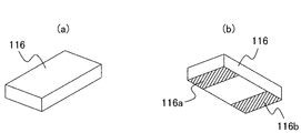
図2(a)および(b)は上記回路部品を示す概略図であり、それぞれ上部斜視図および下部斜視図である。 2 (a) and 2 (b) are schematic views showing the circuit component, and are an upper perspective view and a lower perspective view, respectively.
図2(a)および(b)に示すように、この回路部品116は、直方体形状を有し、その裏面の両端部には該プリント基板の実装パターンにはんだなどで固着される実装面116aおよび116bが形成されている。ここで、該実装面は、例えば、はんだ付け可能となるよう、メタライズ処理などが施されている。
As shown in FIGS. 2A and 2B, the
また、上記実装パターンは、上記信号配線111の、実装する回路部品116の一端側実装面116aが位置する実装面配置部位Aの両側にこれを挟むよう配置された一対のランドのパターン(部品実装用ランドパターン)112aおよび112bと、該信号配線101の、該実装する回路部品116の他端側実装面116bが位置する実装面配置部位Bの両側にこれを挟むよう配置された一対のランドのパターン(部品実装用ランドパターン)122aおよび122bとを有しており、これらのランドパターンには、上記回路部品116の実装面116aおよび116bが固着される。
In addition, the mounting pattern is a pattern of a pair of lands arranged on both sides of the mounting surface arrangement part A where the one end
また、上記実装パターンは、該信号配線111の両側に該信号配線111およびランドパターン112a、112b、122a、122bを囲むよう配置され、該信号配線111をシールドするシールド用パターン113aおよび113bと、該ランドパターン112aとシールド用ランドパターン113aとを接続する接続導体パターン114aおよび114cと、該ランドパターン112bとシールド用ランドパターン113bとを接続する接続導体パターン114bおよび114dと、該ランドパターン122aとシールド用ランドパターン113aとを接続する接続導体パターン124aおよび124cと、該ランドパターン122bとシールド用ランドパターン113bとを接続する接続導体パターン124bおよび124dとを有している。
The mounting pattern is disposed on both sides of the
ここで、上記シールド用ランドパターン113a、ランドパターン112aおよび122a、並びに、接続導体パターン114a、114c、124a、124cは、それぞれの側辺が上記信号配線111のこれらのパターンに対向する一側辺と平行な一直線上に位置するよう配置されている。また、上記シールド用ランドパターン113b、ランドパターン112bおよび122b、並びに、接続導体パターン114b、114d、124b、124dは、それぞれの側辺が上記信号配線111のこれらのパターンに対向する他の側辺と平行な一直線上に位置するよう配置されている。
Here, the
また、上記信号配線111の、上記2つの実装面配置部位AおよびBの間に位置する部分115は、該実装面配置部位AおよびBに跨って回路部品116が実装されるときは、該部分115で信号配線116が切断されるよう配線材料が取り除かれ、回路部品116が実装されないときは、そのまま配線の一部として残される。
In addition, when the
このように本実施形態1のプリント基板100では、該基板上での部品実装のための領域を形成する実装パターンは、上記信号配線111を挟む2組のランドパターン112a、112b、122a、および122bと、該信号配線111のシールド用パターン113aおよび113bと、ランドパターンとシールド用ランドパターンとを接続する接続導体パターン114a〜114dおよび124a〜124dとで構成されている。従って、このような実装パターンを有するプリント基板100では、上記信号配線111の、実装面配置部位AおよびBの間に位置する部分115を除去して、この部分115で該信号配線を切断し、上記回路部品116を、その両端の実装面116aおよび116bが該実装面配置部位AおよびBに固着されるよう実装することにより、該回路部品116を該信号配線111に直列に接続されるよう実装することができる。
As described above, in the printed
また、部品未実装時には、上記信号配線111は部品実装のために形状を変えることなく、また、信号配線111の両側に配置されたシールド用パターン113aおよび113bによる信号配線のシールドも、ランドパターン112a、112b、124aおよび124bによって途切れることはない。
Further, when the component is not mounted, the
なお、本実施形態1では、各ランドパターンは、左右2箇所でシールド用パターンと接続されているが、ランドパターンを接続導体パターンによりシールド用パターンと接続する箇所および接続面積は、上記実施形態1で示したものに限定されるものではない。 In the first embodiment, each land pattern is connected to the shielding pattern at two places on the left and right. However, the place and the connection area where the land pattern is connected to the shielding pattern by the connection conductor pattern are the same as those in the first embodiment. It is not limited to what was shown by.
次に回路部品の実装方法について説明する。 Next, a circuit component mounting method will be described.
図3(a)および図3(b)は、図1に示すプリント基板に回路部品を実装する方法を説明する図であり、図3(a)は部品実装前に上記信号配線の部品実装箇所を断線させた状態を示し、図3(b)は、該部品実装領域に回路部品を実装した状態を示している。 FIGS. 3A and 3B are views for explaining a method of mounting circuit components on the printed circuit board shown in FIG. 1, and FIG. 3A is a component mounting portion of the signal wiring before component mounting. FIG. 3B shows a state in which circuit components are mounted in the component mounting region.
図1に示すプリント基板100のランドパターン112a、112b、122a、および122bが配置された、所定の部品実装領域に回路部品を配置する場合は、図3(a)に示すように、該信号配線111の、部品配置部位AおよびBの間に位置する部分115を除去して、この部分(信号配線カット部)115で該信号配線111を断線させ、さらに、上記接続導体パターン114a〜114dおよび124a〜124dを除去する。
When circuit components are arranged in a predetermined component mounting area where the
次に、図3(b)に示すように、上記回路部品116を、その両端の実装面116aおよび116bが該部品配置部位AおよびBに固着されるよう実装する。その際、接続点117および127にて、上記回路部品160の各実装面116aおよび116bと該信号配線111も接続する。これにより、該回路部品を、上記信号配線111に直列に挿入されるよう実装することが可能となる。
Next, as shown in FIG. 3B, the
なお、この回路部品116の実装の際、あらかじめランドパターン112a、112b、122a、122bと信号配線111の接続点117および127とを、導体層(補強導体層)などで接続した後に、該導体層により接続された導体部分に回路部品116の各実装面116aおよび116bを固着することで、回路部品とプリント基板との接続の強化を図るなどしても良い。
When the
このように本実施形態では、プリント基板100上に形成され、部品実装領域および信号配線を構成する導体層の平面パターンを、該信号配線111の平面パターンである配線パターンと、該部品実装領域の平面パターンである実装パターンとに分離したので、信号配線111のパターン形状を変更することなく、部品実装用ランドパターン112a、112b、122a、122bを配置することができる。
As described above, in the present embodiment, the planar pattern of the conductor layer formed on the printed
また、部品実装時は、上記信号配線111を、その回路部品116の下側に位置する部分115で断線させ、該回路部品116を、該部品実装領域内のランドパターンに実装する際に、該回路部品の実装面116aおよび116bを、該ランドパターンだけでなく該断線部分の両側の信号配線111にも接続することで、該信号配線上に部品実装用パターンを設置せずに、該信号配線111に直列に回路部品116を接続することができる。
Further, when mounting the component, the
また、上記信号配線の両側にはシールド層を、上記部品実装用ランドを囲むよう配置しているので、部品実装用ランドパターンと信号配線のシールドパターンとを接続した構造により、部品未実装状態で上記信号配線に対するシールドパターンが途切れるのを防止でき、これにより該信号配線のシールド不良によって該信号配線に弊害が発生するのを防止することができる。 In addition, since the shield layer is arranged on both sides of the signal wiring so as to surround the component mounting land, the structure in which the component mounting land pattern and the signal wiring shield pattern are connected to each other in the unmounted state. It is possible to prevent the shield pattern for the signal wiring from being interrupted, thereby preventing the signal wiring from being adversely affected by the shielding failure of the signal wiring.
また、部品実装用ランドパターンとこれに隣接する信号配線部分とを補強導体層で接続することにより、実装された回路部品と信号配線および部品実装用ランドパターンとの接続強度を高めることができる。 In addition, by connecting the component mounting land pattern and the signal wiring portion adjacent thereto with the reinforcing conductor layer, the connection strength between the mounted circuit component, the signal wiring, and the component mounting land pattern can be increased.
なお、上記実施形態1では、信号配線116の断線部分115は、手作業で導電層を除去するようにしているが、該断線部分を除去する方法はこれに限るものではなく、あらかじめ、該信号配線と同幅の導体層などで断線位置を導通させておき、部品実装時に上記導体層を取り外すことで断線状態としても良い。
In the first embodiment, the conductive layer is manually removed from the
以下、図4を用いて上記信号配線の断線部分を断線させる他の方法を説明する。 Hereinafter, another method for disconnecting the disconnected portion of the signal wiring will be described with reference to FIG.
この方法は、図4に示すプリント基板100aを用いるものである。
This method uses a printed
該プリント基板100aは、図1に示すプリント基板100の信号配線111に代えて、部品実装領域の中央で分断した構造の信号配線111aを備え、該信号配線111aの分断部分115を、該信号配線111aと同一の幅を有する導体部材115aで接続したものである。
The printed
なお、図4に示すプリント基板100aのその他の部分は、図1に示すプリント基板100におけるものと同一である。
The other parts of the printed
このような構造のプリント基板100aでは、その部品実装領域における上記信号配線111aの分断部分115が導体部材115aにより予め接続された状態となっているので、該部品実装領域に回路部品を実装する場合、該導体部材115aを取り外し、その後、上記実施形態1と同様に、該部品実装領域に回路部品を実装する。
In the printed
このような構造のプリント基板100aにおいても、該部品実装領域に回路部品を実装しない場合は、部品実装領域で信号配線の幅が変化するのを回避することができる。
Even in the printed
このように図4に示すプリント基板100aでは、上記信号配線を、部品実装領域内に位置する部分で分断し、かつ該信号配線の分断した部分を、該信号配線を構成する導電層とは異なる導体層により電気的に接続した構造としているので、部品実装領域に回路部品を実装する際には、該信号配線を該部品実装領域で容易に断線させることができる。
(実施形態2)
図5および図6は、本発明の実施形態2によるプリント基板を説明する平面図であり、図5は、該プリント基板に形成された部品実装用ランドパターンを示し、図6は、該プリント基板に回路部品を実装した状態を示している。
As described above, in the printed
(Embodiment 2)
5 and 6 are plan views for explaining a printed circuit board according to Embodiment 2 of the present invention. FIG. 5 shows a land pattern for component mounting formed on the printed circuit board. FIG. 6 shows the printed circuit board. Shows a state where circuit components are mounted.
この実施形態2のプリント基板100bは、絶縁材料で構成された絶縁板101の表面に所定パターンを有する金属材料などの導電材料からなる導電層を形成してなるものであり、該導電層は、電子回路を構成する所定のパターンを有する信号配線111bと、電子回路を構成する回路部品116を実装するための所定のパターンを有する部品実装領域(以下、実装パターンという。)とを有している。なお、以下、上記部品実装領域の平面パターンは実装パターンともいう。また、該回路部品116は、図2に示すものと同一のものである。
The printed
ここで、該実装パターンは、上記信号配線の一方側に隣接して配置されたランドパターン132と、該信号配線111bに沿ってその一方側に、該信号配線111bを囲むよう配置され、該信号配線111bをシールドするシールド用パターン133と、該ランドパターン132とシールド用ランドパターン133とを接続する接続導体パターン134aおよび134bと、該信号配線の他方側にこれに沿って配置された第2のランドパターン138とを有している。
Here, the mounting pattern is disposed so as to surround the
ここで、第2のランドパターン138は、接地電位を供給するグランド電位供給配線のパターンを兼ねるものである。ただし、第2のランドパターン138は、電源電位を供給する電源電位供給配線のパターンを兼ねるものであってもよい。上記シールド用ランドパターン133、ランドパターン132および接続導体パターン134a、134bは、それぞれの側辺が上記信号配線111bの、これらのパターンに対向する一側辺と平行な一直線上に位置するよう配置されている。
Here, the
このように本実施形態2のプリント基板100では、該基板上での部品実装領域を形成する実装パターンは、信号配線111bの所定箇所の一方側に配置されたランドパターン132と、該信号配線111bの一方側に配置されたシールド用パターン133と、ランドパターンとシールド用ランドパターンとを接続する接続導体パターン134a〜134bと、該信号配線111bの他方側に配置された第2のランドパターン138とで構成されている。従って、このような実装パターンを有するプリント基板100bでは、上記信号配線111bの部品実装領域に、上記回路部品116をその両端の実装面116aおよび116bが該第1および第2のランドパターン132および138に固着されるよう実装することにより、該回路部品を信号配線と接地ラインとの間に接続されるよう実装することができる。
As described above, in the printed
また、上記信号配線は、部品未実装時に、該信号配線に接続されるよう回路部品の実装を可能としたことによる形状変化が生じることのないものとなり、また、信号配線111bの一方側に配置されたシールド用パターン133もランドパターンと接続されているので、信号配線111の一方側でそのシールド部分がランドパターンによって電気的に途切れることはない。
In addition, the signal wiring does not change in shape due to the fact that the circuit component can be mounted so as to be connected to the signal wiring when the component is not mounted, and is arranged on one side of the
次に実装方法について簡単に説明する。 Next, the mounting method will be briefly described.
また、図5に示すプリント基板100bのランドパターン132および138が配置された、所定の部品実装領域に回路部品116を配置する場合は、図6に示すように、上記接続導体パターン134aおよび134bを除去し、その後、上記回路部品116を、その両端の実装面116aおよび116bが該第1および第2のランドパターン132および138に固着されるよう実装する。その際、接続点137にて、該回路部品116と信号配線111bも接続する。これにより、該回路部品116を、該信号配線111bと電源あるいは接地ラインとしての第2のランドパターン138の間に接続して実装することが可能となる。
Further, when the
また、上記信号配線の両側に、第1の部品実装用ランドパターンと第2の部品実装用ランドパターンとを配置しているので、該部品実装用ランドパターンは、上記信号配線の形状を変化させることなく配置することができる。また、部品実装時は、上記回路部品を、該部品実装用ランドパターンと共に上記信号配線と接続することで、該該回路部品を、該信号配線と、該部品実装用ランドパターンを兼ねる他の配線パターンとの間に接続することができる。 In addition, since the first component mounting land pattern and the second component mounting land pattern are arranged on both sides of the signal wiring, the component mounting land pattern changes the shape of the signal wiring. It can arrange without. Further, at the time of component mounting, the circuit component is connected to the signal wiring together with the component mounting land pattern, whereby the circuit component is connected to the signal wiring and another wiring that also serves as the component mounting land pattern. Can be connected between the pattern.
なお、本実施形態2では、第1のランドパターンは、左右2箇所でシールド用パターンと接続されているが、該第1のランドパターンを接続導体パターンによりシールド用パターンと接続する箇所および接続面積は、上記実施形態2で示したものに限定されるものではない。 In the second embodiment, the first land pattern is connected to the shield pattern at two places on the left and right, but the place and the connection area where the first land pattern is connected to the shield pattern by the connection conductor pattern. Is not limited to that shown in the second embodiment.
また、部品実装の際、あらかじめ第1のランドパターン132と信号配線111bの接続点137とを導体部材(補強導体層)などで接続した後に、上記導体部材により接続された導体部分に上記回路部品116の各実装面を固着することで、該回路部品とプリント基板との接続の強化を図るなどしても良い。
In addition, when the component is mounted, the
以上のように、本発明の好ましい実施形態を用いて本発明を例示してきたが、本発明は、この実施形態に限定して解釈されるべきものではない。本発明は、特許請求の範囲によってのみその範囲が解釈されるべきであることが理解される。当業者は、本発明の具体的な好ましい実施形態の記載から、本発明の記載および技術常識に基づいて等価な範囲を実施することができることが理解される。本明細書において引用した特許、特許出願および文献は、その内容自体が具体的に本明細書に記載されているのと同様にその内容が本明細書に対する参考として援用されるべきであることが理解される。 As mentioned above, although this invention has been illustrated using preferable embodiment of this invention, this invention should not be limited and limited to this embodiment. It is understood that the scope of the present invention should be construed only by the claims. It is understood that those skilled in the art can implement an equivalent range based on the description of the present invention and the common general technical knowledge from the description of specific preferred embodiments of the present invention. Patents, patent applications, and documents cited herein should be incorporated by reference in their entirety, as if the contents themselves were specifically described herein. Understood.
本発明は、回路部品を実装するための複数の部品実装領域を有するプリント基板の分野において、該回路部品を実装していない部品実装領域で信号配線の配線幅が変化してしまうのを回避することができ、これにより、高周波信号線にも適用できるプリント基板の導体パターン構造を提供することができる。 In the field of a printed circuit board having a plurality of component mounting areas for mounting circuit components, the present invention avoids a change in signal wiring width in a component mounting area in which the circuit components are not mounted. Thus, it is possible to provide a printed circuit board conductor pattern structure that can also be applied to high-frequency signal lines.
100、100a、100b プリント基板
101 絶縁板
111、111a、111b 信号配線
112a、112b、122a、122b、132 部品実装用ランドパターン
113a、113b 133シールド用ランドパターン
114a〜114d、124a〜124d、134a、134b ランドパターン接続用導体
115 信号配線カット部
115a 配線接続導体
116 回路部品(実装部品)
116a、116b 実装面
117、137 電気的接続部
138 接地ランドパターン
100, 100a, 100b Printed
116a,
Claims (20)
該回路部品を実装するための部品実装領域と、
該回路部品に接続される部品接続部を有する少なくとも1つの信号配線とを備え、
該部品実装部は、該信号配線の、その両側に該信号配線に接続される回路部品を支持する領域として該部品実装領域が配置されている部分であり、
該信号配線は、その配線幅が少なくとも該部品接続部で変化しない構造を有し、
該信号配線および該部品実装領域は導体層により構成され、
該導体層の平面パターンは、該信号配線の平面パターンである配線パターンと、該部品実装領域の平面パターンである実装パターンとに分離されているプリント基板。 A printed circuit board for configuring an electronic circuit by mounting circuit components,
Component mounting area for mounting the circuit component;
And at least one signal wiring having a component connecting portion connected to the circuit component,
The component mounting portion is a portion where the component mounting area is arranged as an area for supporting circuit components connected to the signal wiring on both sides of the signal wiring,
The signal wiring has a structure in which the wiring width does not change at least at the component connection portion,
The signal wiring and the component mounting area are constituted by a conductor layer,
The printed circuit board in which the planar pattern of the conductor layer is separated into a wiring pattern that is a planar pattern of the signal wiring and a mounting pattern that is a planar pattern of the component mounting region.
前記実装パターンは、
前記回路部品の実装面が配置される部品実装用ランドのパターンとして、
前記信号配線の一方の側辺に沿って互いに隣接するよう配置された第1および第2の部品実装用ランドのパターンと、
該信号配線の他方の側辺に沿って互いに隣接するよう配置された第3および第4の部品実装用ランドのパターンとを含み、
該第1および第3の部品実装用ランドは、該信号配線を挟んで互いに対向するよう位置しており、
該第2および第4の部品実装用ランドは、該信号配線を挟んで互いに対向するよう位置しているプリント基板。 The printed circuit board according to claim 1,
The mounting pattern is
As a component mounting land pattern on which the circuit component mounting surface is arranged,
A pattern of first and second component mounting lands disposed adjacent to each other along one side of the signal wiring;
A pattern of third and fourth component mounting lands arranged adjacent to each other along the other side of the signal wiring,
The first and third component mounting lands are positioned to face each other across the signal wiring,
The printed circuit board in which the second and fourth component mounting lands are positioned so as to face each other with the signal wiring interposed therebetween.
前記第1および第3の部品実装用ランドは、前記回路部品の一端側実装面が配置されるランドであり、
前記第2および第4の部品実装用ランドは、該回路部品の他端側実装面が配置されるランドであるプリント基板。 The printed circuit board according to claim 2,
The first and third component mounting lands are lands on which one end side mounting surfaces of the circuit components are disposed,
The second and fourth component mounting lands are printed circuit boards which are lands on which the other end mounting surface of the circuit component is disposed.
前記信号配線は、前記回路部品を前記部品実装領域に実装したとき、該回路部品が該信号配線に直列に接続されるよう、該回路部品の一端側実装面とその他端側実装面との間に対応する部分で分断されるものであるプリント基板。 The printed circuit board according to claim 3,
The signal wiring is provided between one end mounting surface and the other end mounting surface of the circuit component so that the circuit component is connected in series to the signal wiring when the circuit component is mounted in the component mounting region. Printed circuit board that is divided at the part corresponding to.
前記第1および第3の部品実装用ランドと、前記信号配線の、これらのランドの間に位置する部分とは、該信号配線を構成する導体層とは異なる第1の補強導体層により接続されており、
前記第2および第4の部品実装用ランドと、該信号配線の、これらのランドの間に位置する部分とは、該信号配線を構成する導体層とは異なる第2の補強導体層により接続されており、
該第1の補強導体層により接続された導体部分は、前記回路部品の一端側実装面が固着される部分であり、
該第2の補強導体層により接続された導体部分は、該回路部品の他端側実装面が固着される部分であるプリント基板。 The printed circuit board according to claim 2,
The first and third component mounting lands and the portion of the signal wiring located between the lands are connected by a first reinforcing conductor layer different from the conductor layer constituting the signal wiring. And
The second and fourth component mounting lands and the portion of the signal wiring located between the lands are connected by a second reinforcing conductor layer different from the conductor layer constituting the signal wiring. And
The conductor portion connected by the first reinforcing conductor layer is a portion to which the one end side mounting surface of the circuit component is fixed,
The printed circuit board, wherein the conductor part connected by the second reinforcing conductor layer is a part to which the mounting surface on the other end side of the circuit component is fixed.
前記信号配線は、前記第1および第3の部品実装用ランドが対向する部分と、前記第2および第4の部品実装用ランドが対向する部分との間で分断されており、
該信号配線の分断された部分は、該信号配線を構成する導電層とは異なる導体層により電気的に接続されているプリント基板。 The printed circuit board according to claim 2,
The signal wiring is divided between a portion where the first and third component mounting lands face each other and a portion where the second and fourth component mounting lands face each other,
The printed circuit board in which the divided portion of the signal wiring is electrically connected by a conductive layer different from the conductive layer constituting the signal wiring.
前記信号配線の分断された部分を電気的に接続する導体層は、該信号配線の配線幅と同一の幅を有するプリント基板。 The printed circuit board according to claim 6,
The conductor layer that electrically connects the divided portions of the signal wiring is a printed circuit board having the same width as the wiring width of the signal wiring.
前記信号配線の分断された部分を電気的に接続する導体層は、前記回路部品の実装時に除去されるものであるプリント基板。 The printed circuit board according to claim 7,
A printed circuit board in which the conductor layer that electrically connects the divided portions of the signal wiring is removed when the circuit component is mounted.
前記実装パターンは、
前記信号配線の一方の側辺側に、該信号配線に沿って、かつ前記第1および第3の部品実装用ランドを囲むよう配置され、該信号配線をシールドする第1のシールド層のパターンと、
該信号配線の他方の側辺側に、該信号配線に沿って、かつ前記第2および第4の部品実装用ランドを囲むよう配置され、該信号配線をシールドする第2のシールド層のパターンとを含むプリント基板。 The printed circuit board according to claim 2,
The mounting pattern is
A pattern of a first shield layer disposed on one side of the signal wiring along the signal wiring and surrounding the first and third component mounting lands, and shielding the signal wiring; ,
A pattern of a second shield layer disposed on the other side of the signal wiring along the signal wiring and surrounding the second and fourth component mounting lands and shielding the signal wiring; Including printed circuit board.
前記実装パターンは、
前記信号配線の一方の側辺側に位置する第1および第2の部品実装用ランドを前記第1のシールド層と電気的に接続する第1の接続導体のパターンと、
前記信号配線の他方の側辺側に位置する第3および第4の部品実装用ランドを前記第2のシールド層と電気的に接続する第2の接続導体のパターンとを含むプリント基板。 The printed circuit board according to claim 9, wherein
The mounting pattern is
A pattern of first connection conductors for electrically connecting the first and second component mounting lands located on one side of the signal wiring to the first shield layer;
A printed circuit board including a second connection conductor pattern for electrically connecting the third and fourth component mounting lands located on the other side of the signal wiring to the second shield layer.
前記第1のシールド層、前記第1および第2の部品実装用ランド、および前記第1の接続導体は、該信号配線の一方の側辺側に該信号配線に対する連続したシールド部を形成するよう配置されており、
前記第2のシールド層、前記第3および第4の部品実装用ランド、および前記第2の接続導体は、該信号配線の他方の側辺側に該信号配線に対する連続したシールド部を形成するよう配置されているプリント基板。 The printed circuit board according to claim 10,
The first shield layer, the first and second component mounting lands, and the first connection conductor form a continuous shield portion for the signal wiring on one side of the signal wiring. Has been placed,
The second shield layer, the third and fourth component mounting lands, and the second connection conductor form a continuous shield portion for the signal wiring on the other side of the signal wiring. Printed circuit board that is placed.
前記実装パターンは、
前記回路部品の実装面が配置される部品実装用ランドのパターンとして、
前記信号配線の一方の側辺側に位置するよう配置された第1の部品実装用ランドのパターンと、
該信号配線の他方の側辺側に位置するよう配置された第2の部品実装用ランドのパターンとを含むプリント基板。 The printed circuit board according to claim 1,
The mounting pattern is
As a component mounting land pattern on which the circuit component mounting surface is arranged,
A pattern of first component mounting lands arranged to be positioned on one side of the signal wiring;
And a second component mounting land pattern disposed on the other side of the signal wiring.
前記第1の部品実装用ランドは、前記回路部品の一端側実装面が配置されるランドであり、
該第2の部品実装用ランドは、該回路部品の他端側実装面が配置されるランドであるプリント基板。 The printed circuit board according to claim 12, wherein
The first component mounting land is a land on which one end side mounting surface of the circuit component is disposed,
The second component mounting land is a printed circuit board which is a land on which a mounting surface on the other end side of the circuit component is disposed.
前記第2の部品実装用ランドは、前記回路部品に電源電位あるいは接地電位を供給する電位供給配線を兼ねるものであるプリント基板。 The printed circuit board according to claim 13,
The second component mounting land also serves as a potential supply wiring for supplying a power supply potential or a ground potential to the circuit component.
前記回路部品の一端側実装面は、該回路部品を前記部品実装領域に実装したとき、前記信号配線と電気的に接続されるものであるプリント基板。 The printed circuit board according to claim 14, wherein
A printed circuit board in which the one end side mounting surface of the circuit component is electrically connected to the signal wiring when the circuit component is mounted in the component mounting region.
前記第1の部品実装用ランドと、前記信号配線の、該第1の部品実装用ランドと対向する部分とは、該信号配線を構成する導体層とは異なる補強導体層により接続されており、
該補強導体層により接続された導体部分は、前記回路部品の一端側実装面が固着される部分であるプリント基板。 The printed circuit board according to claim 12, wherein
The first component mounting land and the portion of the signal wiring facing the first component mounting land are connected by a reinforcing conductor layer different from a conductor layer constituting the signal wiring,
The printed circuit board, wherein the conductor portion connected by the reinforcing conductor layer is a portion to which the one end side mounting surface of the circuit component is fixed.
前記実装パターンは、
前記信号配線の一方の側辺側に、該信号配線に沿って、かつ前記第1の部品実装用ランドを囲むよう配置され、該信号配線をシールドするシールド層のパターンを含むプリント基板。 The printed circuit board according to claim 12, wherein
The mounting pattern is
A printed circuit board including a pattern of a shield layer disposed on one side of the signal wiring along the signal wiring and surrounding the first component mounting land, and shielding the signal wiring.
前記実装パターンは、
前記信号配線の一方の側辺側に位置する第1の部品実装用ランドを前記シールド層と電気的に接続する接続導体のパターンを有するプリント基板。 The printed circuit board according to claim 17,
The mounting pattern is
A printed circuit board having a pattern of connection conductors for electrically connecting a first component mounting land located on one side of the signal wiring to the shield layer.
前記シールド層、前記第1の部品実装用ランド、および前記接続導体は、前記信号配線の一方の側辺側に該信号配線に対する連続したシールド部を形成するよう配置されているプリント基板。 The printed circuit board according to claim 18,
The printed circuit board, wherein the shield layer, the first component mounting land, and the connection conductor are arranged to form a continuous shield portion for the signal wiring on one side of the signal wiring.
該回路部品を実装するための部品実装領域と、
該回路部品に接続される部品接続部を有する少なくとも1つの信号配線とを備え、
該部品実装部は、該信号配線の、その両側に該信号配線に接続される回路部品を支持する領域として該部品実装領域が配置されている部分であり、
該信号配線は、その配線幅が少なくとも該部品接続部で変化しない構造を有し、
該信号配線および該部品実装領域は導体層により構成され、
該導体層の平面パターンは、該信号配線の平面パターンである配線パターンと、該部品実装領域の平面パターンである実装パターンとに分離されているプリント基板の導体パターン構造。
A printed circuit board conductor pattern structure for mounting circuit components to form an electronic circuit,
Component mounting area for mounting the circuit component;
And at least one signal wiring having a component connecting portion connected to the circuit component,
The component mounting portion is a portion where the component mounting area is arranged as an area for supporting circuit components connected to the signal wiring on both sides of the signal wiring,
The signal wiring has a structure in which the wiring width does not change at least at the component connection portion,
The signal wiring and the component mounting area are constituted by a conductor layer,
A conductor pattern structure of a printed circuit board in which the planar pattern of the conductor layer is separated into a wiring pattern that is a planar pattern of the signal wiring and a mounting pattern that is a planar pattern of the component mounting region.
Priority Applications (1)
| Application Number | Priority Date | Filing Date | Title |
|---|---|---|---|
| JP2007306490A JP4981637B2 (en) | 2007-11-27 | 2007-11-27 | Printed circuit board and conductor pattern structure thereof |
Applications Claiming Priority (1)
| Application Number | Priority Date | Filing Date | Title |
|---|---|---|---|
| JP2007306490A JP4981637B2 (en) | 2007-11-27 | 2007-11-27 | Printed circuit board and conductor pattern structure thereof |
Publications (2)
| Publication Number | Publication Date |
|---|---|
| JP2009130290A JP2009130290A (en) | 2009-06-11 |
| JP4981637B2 true JP4981637B2 (en) | 2012-07-25 |
Family
ID=40820866
Family Applications (1)
| Application Number | Title | Priority Date | Filing Date |
|---|---|---|---|
| JP2007306490A Expired - Fee Related JP4981637B2 (en) | 2007-11-27 | 2007-11-27 | Printed circuit board and conductor pattern structure thereof |
Country Status (1)
| Country | Link |
|---|---|
| JP (1) | JP4981637B2 (en) |
Families Citing this family (2)
| Publication number | Priority date | Publication date | Assignee | Title |
|---|---|---|---|---|
| JP5439900B2 (en) * | 2009-03-30 | 2014-03-12 | 株式会社村田製作所 | Land structure |
| JP6332958B2 (en) * | 2013-12-18 | 2018-05-30 | キヤノン株式会社 | Electronic component mounting structure, printed wiring board, and electronic equipment |
Family Cites Families (9)
| Publication number | Priority date | Publication date | Assignee | Title |
|---|---|---|---|---|
| JPS59135662U (en) * | 1983-02-28 | 1984-09-10 | 株式会社リコー | Wiring pattern structure |
| JPH0786729A (en) * | 1993-09-09 | 1995-03-31 | Ibiden Co Ltd | Connection structure of jumper land in printed-wiring board and connection of jumper land |
| JPH07154037A (en) * | 1993-11-26 | 1995-06-16 | Sony Corp | Short land structure for printed board |
| JPH07183627A (en) * | 1993-12-22 | 1995-07-21 | Rohm Co Ltd | Printed circuit board |
| JP3698311B2 (en) * | 2001-03-06 | 2005-09-21 | 船井電機株式会社 | Wiring board device |
| JP2003198113A (en) * | 2001-12-28 | 2003-07-11 | Toshiba Corp | Printed wiring board, circuit module having printed wiring board, and electronic equipment mounting circuit module |
| JP2005167045A (en) * | 2003-12-04 | 2005-06-23 | Mitsubishi Electric Corp | Electronic component and its manufacturing method |
| JP4415769B2 (en) * | 2004-06-25 | 2010-02-17 | 船井電機株式会社 | Printed circuit board having chip land |
| JP2007258654A (en) * | 2006-03-22 | 2007-10-04 | Taiyo Yuden Co Ltd | Circuit board land connection method and the circuit board |
-
2007
- 2007-11-27 JP JP2007306490A patent/JP4981637B2/en not_active Expired - Fee Related
Also Published As
| Publication number | Publication date |
|---|---|
| JP2009130290A (en) | 2009-06-11 |
Similar Documents
| Publication | Publication Date | Title |
|---|---|---|
| US20050087366A1 (en) | Insertion of electrical component within a via of a printed circuit board | |
| EP2388867A2 (en) | Electrical connector having thick film layers | |
| US11013117B2 (en) | Electronic device with built in fuse | |
| JP3935529B2 (en) | Printed circuit board | |
| US7411474B2 (en) | Printed wiring board assembly with self-compensating ground via and current diverting cutout | |
| US7412923B2 (en) | Stencil device for accurately applying solder paste to a printed circuit board | |
| JP4981637B2 (en) | Printed circuit board and conductor pattern structure thereof | |
| US9769925B2 (en) | Relieved component pad for 0201 use between vias | |
| US9538636B1 (en) | Blind via edge castellation | |
| JP2010238755A (en) | Land structure | |
| KR20200082291A (en) | Printed Circuit Board | |
| JP6338784B1 (en) | Noise filter | |
| KR102382391B1 (en) | Printed Circuit Board | |
| US7140531B2 (en) | Method of fabricating a substantially zero signal degradation electrical connection on a printed circuit broad | |
| KR101842206B1 (en) | Z-directed capacitor components for printed circuit boards | |
| JP4496619B2 (en) | Circuit board connection structure | |
| TW202127974A (en) | Resistive pcb traces for improved stability | |
| JP2012084799A (en) | Electronic circuit | |
| JP6465611B2 (en) | Electronic component, wiring board with built-in electronic component, and manufacturing method thereof | |
| JP5454991B2 (en) | Land structure | |
| JP4803071B2 (en) | Circuit board and circuit board with electronic components | |
| JP4491338B2 (en) | Semiconductor device substrate and semiconductor device | |
| JP2003283285A (en) | Noise filter and its mounting structure | |
| KR102667536B1 (en) | Hybrid inductor | |
| JPH0992952A (en) | Printed pattern element |
Legal Events
| Date | Code | Title | Description |
|---|---|---|---|
| A621 | Written request for application examination |
Free format text: JAPANESE INTERMEDIATE CODE: A621 Effective date: 20100218 |
|
| A131 | Notification of reasons for refusal |
Free format text: JAPANESE INTERMEDIATE CODE: A131 Effective date: 20111213 |
|
| A521 | Written amendment |
Free format text: JAPANESE INTERMEDIATE CODE: A523 Effective date: 20120110 |
|
| TRDD | Decision of grant or rejection written | ||
| A01 | Written decision to grant a patent or to grant a registration (utility model) |
Free format text: JAPANESE INTERMEDIATE CODE: A01 Effective date: 20120330 |
|
| A01 | Written decision to grant a patent or to grant a registration (utility model) |
Free format text: JAPANESE INTERMEDIATE CODE: A01 |
|
| A61 | First payment of annual fees (during grant procedure) |
Free format text: JAPANESE INTERMEDIATE CODE: A61 Effective date: 20120420 |
|
| FPAY | Renewal fee payment (event date is renewal date of database) |
Free format text: PAYMENT UNTIL: 20150427 Year of fee payment: 3 |
|
| R150 | Certificate of patent or registration of utility model |
Free format text: JAPANESE INTERMEDIATE CODE: R150 |
|
| RD04 | Notification of resignation of power of attorney |
Free format text: JAPANESE INTERMEDIATE CODE: R3D04 |
|
| LAPS | Cancellation because of no payment of annual fees |