JP4980873B2 - Superconducting connection part to which superconducting wire is connected and method for producing the same - Google Patents
Superconducting connection part to which superconducting wire is connected and method for producing the same Download PDFInfo
- Publication number
- JP4980873B2 JP4980873B2 JP2007333745A JP2007333745A JP4980873B2 JP 4980873 B2 JP4980873 B2 JP 4980873B2 JP 2007333745 A JP2007333745 A JP 2007333745A JP 2007333745 A JP2007333745 A JP 2007333745A JP 4980873 B2 JP4980873 B2 JP 4980873B2
- Authority
- JP
- Japan
- Prior art keywords
- superconducting
- metal sleeve
- melting point
- metal
- connection part
- Prior art date
- Legal status (The legal status is an assumption and is not a legal conclusion. Google has not performed a legal analysis and makes no representation as to the accuracy of the status listed.)
- Expired - Fee Related
Links
- DBAFGDDSIBADQU-UHFFFAOYSA-N C1C2C3C4=[O]CCC4CC2C13 Chemical compound C1C2C3C4=[O]CCC4CC2C13 DBAFGDDSIBADQU-UHFFFAOYSA-N 0.000 description 1
Images


Description
本発明は、超電導フィラメントが、母材に覆われた構造を有する超電導線材を接続した超電導接続部およびその作製方法に関する。 The present invention relates to a superconducting connection portion in which a superconducting filament is connected to a superconducting wire having a structure covered with a base material, and a method for manufacturing the same.
超電導線材を用いた製品の1つに、超電導マグネットがある。超電導マグネットは、例えば、医療用核磁気共鳴画像(MRI:Magnetic Resonance Imaging)装置および核磁気共鳴(NMR:Nuclear Magnetic Resonance)装置に用いられる。 One of products using superconducting wire is a superconducting magnet. Superconducting magnets are used in, for example, medical nuclear magnetic resonance imaging (MRI) devices and nuclear magnetic resonance (NMR) devices.
超電導マグネットには、液体ヘリウムなどを用いた極低温環境下において電気抵抗がゼロとなる、超電導線材から構成された閉ループが内蔵されている。この閉ループに電流を誘起するときには外部電源を用いるが、所定の電流値に達した後は永久電流スイッチと呼ばれる素子を用いる。これにより、外部電源を切り離しても所定の大きさの電流を保持することが可能となる。このように、外部電源と切り離した状態で、所定の大きさの電流を閉ループに保持することができるような回路を永久電流回路といい、永久電流回路を有する超電導マグネットでは、この保持された電流により長期間に渡って極めて減衰の小さい磁場を発生させることが可能である。 The superconducting magnet has a built-in closed loop made of a superconducting wire that has zero electrical resistance in a cryogenic environment using liquid helium. An external power source is used when inducing current in the closed loop, but after reaching a predetermined current value, an element called a permanent current switch is used. As a result, even when the external power supply is disconnected, a predetermined amount of current can be maintained. A circuit that can hold a current of a predetermined magnitude in a closed loop in a state disconnected from an external power source is called a permanent current circuit. In a superconducting magnet having a permanent current circuit, this held current is Thus, it is possible to generate a magnetic field with extremely small attenuation over a long period of time.
超電導マグネットの作製には、非常に長い超電導線材を必要とし、また、永久電流スイッチなどの素子を永久電流回路内に組み込む必要もある。そのため、永久電流回路を単一の超電導線材から作製することは実質的に不可能である。したがって、超電導線材同士を極めて低い抵抗値、例えば10−13Ω以下で接続する必要がある。 The production of a superconducting magnet requires a very long superconducting wire, and it is also necessary to incorporate elements such as a permanent current switch into the permanent current circuit. Therefore, it is practically impossible to make a permanent current circuit from a single superconducting wire. Therefore, it is necessary to connect the superconducting wires with an extremely low resistance value, for example, 10 −13 Ω or less.
超電導線材の接続を行うには、常電導物質である母材を除去して超電導フィラメント同士を直接接続する、もしくは、超電導フィラメント同士を同種あるいは異種の超電導物質を介して接続する、ことが必要である。 To connect superconducting wires, it is necessary to remove the base material, which is a normal conducting material, and connect the superconducting filaments directly, or connect the superconducting filaments via the same or different superconducting materials. is there.
特許文献1には、超電導線材の端部の母材を、硝酸を用いたエッチングにより除去し、超電導フィラメントを露出させ、露出させた超電導フィラメントを銅等のスリーブに挿入し、スリーブとともに超電導フィラメント同士を一軸にプレスして、超電導線材の接続を行う方法が記載されている。
In
また、特許文献2に記載されている超電導線材の接続方法では、まず、超電導線材の端部を、溶融したスズ浴に浸漬し、母材をスズに置換し、次に、スズ置換した超電導線材の端部を、溶融した鉛ビスマス浴に浸漬して、母材を鉛ビスマスに置換し、次に、鉛ビスマス置換した超電導線材の端部を溶融した鉛ビスマスが充填されたスリーブ内に挿入して冷却固化させる。この方法で接続された超電導接合部は、超電導フィラメント同士が超電導物質である鉛ビスマスを介して接続された構造となっている。 In the method of connecting superconducting wires described in Patent Document 2, first, the end of the superconducting wire is immersed in a molten tin bath, the base material is replaced with tin, and then the tin-substituted superconducting wire is used. The end of the lead is immersed in a molten lead bismuth bath to replace the base material with lead bismuth, and then the end of the lead-bismuth-substituted superconducting wire is inserted into a sleeve filled with molten lead bismuth. To cool and solidify. The superconducting junctions connected by this method have a structure in which superconducting filaments are connected to each other via lead bismuth, which is a superconducting material.
特許文献1の方法では、超電導線材の端部の母材を硝酸で溶解することによって、その部分の超電導フィラメントが大気に晒される。そのため、母材が溶解された超電導フィラメントの表面に酸化膜が形成される。その後、母材が溶解された超電導フィラメント部分を銅等のスリーブの中に挿入し、スリーブとともに超電導フィラメントのプレスを行い、超電導フィラメント同士の密着を行うが、酸化膜の完全な除去は期待できず、超電導フィラメント同士が高抵抗の酸化膜を介して接触している部分が残存する。その結果、超電導接続部がクエンチする電流値がばらついてしまう、もしくは、素線の臨界電流値と比較して著しく低い値となってしまうなどの問題が生じる。
In the method of
また、特許文献2の方法では、超電導フィラメントが大気に晒される工程を含まないため、超電導フィラメント表面の酸化膜の形成は抑制される。しかしながら、近年、環境への配慮から、製品によっては、鉛もしくは鉛合金を適用できない場合があり、鉛ビスマスを用いない環境に配慮した超電導製品に対するニーズがある。 Further, the method of Patent Document 2 does not include a process in which the superconducting filament is exposed to the atmosphere, so that formation of an oxide film on the surface of the superconducting filament is suppressed. However, in recent years, due to environmental considerations, depending on the product, lead or lead alloys may not be applicable, and there is a need for an environmentally friendly superconducting product that does not use lead bismuth.
よって、本発明では、超電導フィラメントの表面に酸化膜が形成されることを抑制するとともに、鉛もしくは鉛合金を用いず環境に配慮した、超電導接続部およびその作製方法を提供することを目的とする。 Accordingly, an object of the present invention is to provide a superconducting connection portion and a method for manufacturing the same, which suppresses the formation of an oxide film on the surface of the superconducting filament and is environmentally friendly without using lead or a lead alloy. .
本発明は、
超電導フィラメントが母材で覆われた構造を有する超電導線材を接続した超電導接続部であって、
前記超電導線材の端部の母材が、鉛若しくは鉛合金を含有せず、かつ、融点が100℃以上500℃以下である低融点金属に置換されている置換部と、前記置換部を覆うための金属製スリーブとを有し、
前記金属製スリーブは、前記低融点金属の融点以上の温度で、加熱され、加熱状態で前記置換部とともに、プレスされ、
前記低融点金属の一部が前記金属製スリーブの外に排出されることによって、前記超電導フィラメント同士が密着している
ことを特徴とする。
The present invention
A superconducting connection part connecting superconducting wires having a structure in which a superconducting filament is covered with a base material,
The base material at the end portion of the superconducting wire does not contain lead or a lead alloy, and the replacement portion is replaced with a low melting point metal having a melting point of 100 ° C. or higher and 500 ° C. or lower, and to cover the replacement portion And a metal sleeve,
The metal sleeve is heated at a temperature equal to or higher than the melting point of the low melting point metal, and is pressed together with the replacement portion in a heated state.
Wherein the portion of the low melting point metal Rukoto is discharged to the outside of the metal sleeve, wherein the superconducting filaments are in close contact.
本発明により、超電導フィラメントの表面に酸化膜が形成されることを抑制するとともに、鉛もしくは鉛合金を用いず環境に配慮した、超電導接続部およびその作製方法を提供することができる。 According to the present invention, it is possible to provide a superconducting connection portion and a method of manufacturing the superconducting connection portion that suppresses the formation of an oxide film on the surface of a superconducting filament and that is environmentally friendly without using lead or lead alloys.
以下、本発明の実施形態について、図面を参照に説明する。まず、本発明の第1実施形態について説明する。 Embodiments of the present invention will be described below with reference to the drawings. First, a first embodiment of the present invention will be described.
第1実施形態での超電導接合部100の作製において用いる超電導線材10の断面の模式図を図1に示す。超電導線材10は、超電導フィラメント1と、母材2と、を有する。超電導フィラメント1は母材2に覆われた構造となっている。超電導線材10の内部には、直径が10〜100μm程度の超電導フィラメント1が20〜3000本程度含まれている。
A schematic diagram of a cross section of the
超電導フィラメント1の材料としては、例えば、ニオブとチタンの合金が用いられる。また、母材2の材料としては、例えば、銅、銅とニッケルの合金が用いられる。
As a material of the
また、第1実施形態での超電導接合部100の作製において用いる金属製スリーブ30は、図2に示すように、両端が開放され、管の中心に孔32を有する。図2(a)に金属製スリーブ30の前面からの断面の模式図と、図2(b)に金属製スリーブ30の側面からの断面の模式図と、を示す。
Moreover, as shown in FIG. 2, the
金属製スリーブ30の材料としては、例えば、銅、ニオブ、タンタル、ニオブとタンタルの複合材が用いられる。
As a material of the
また、金属製スリーブ30の縁部30aによって超電導フィラメント1が断線するのを防止するために、金属製スリーブ30の端部30bにテーパ加工31を施してもよい。
Further, in order to prevent the
そして、金属製スリーブの側面30cに、後述する低融点金属6を排出しやすいように、排出孔を設ける加工を施してもよい。
And processing which provides a discharge hole may be given to
(第1実施形態での作製方法)
次に、第1実施形態の超電導接合部100の作製方法を図3に示し、図3を用いて説明する。
(Production method in the first embodiment)
Next, a method for producing the
まず、超電導線材10の端部10aを、鉛若しくは鉛合金を含有せず、融点が100℃以上500℃以下の低融点金属6が溶融した低融点金属浴(図示しない)に浸し、母材2を低融点金属6への置換する工程を行う(図3のS1)。超電導線材10の端部10aの母材2が低融点金属6に置換された状態の模式図を図4に示す。
First, the
低融点金属6としては、後述する金属スリーブ30を加熱して、プレスする際、超電導線材10の劣化が見られない温度以下に融点をもつ金属であればよく、100℃以上500℃以下に融点を持つ金属であればよい。例えば、スズ、インジウム、スズとインジウムの合金などが用いられ、それぞれの融点は、232℃、157℃、120〜232℃である。
As the low melting point metal 6, any metal having a melting point below the temperature at which deterioration of the
なお、超電導線材10の母材2を低融点金属6に置換する際の、低融点金属浴の適正温度、および、超電導線材10の低融点金属浴への適正浸漬時間は、母材2の材質、母材2の超電導線材10における割合量、超電導フィラメント1の本数、超電導フィラメント1の直径などに依存するため、超電導線材10の母材2が低融点金属6に置換された置換部10cの断面を観察し、母材2が完全に低融点金属6に置換されるような条件を超電導線材10ごとに明らかにする必要がある。
The appropriate temperature of the low melting point metal bath and the proper immersion time of the
次に、超電導線材10の置換部10cを金属製スリーブ30に挿入する工程を行う(図3のS2)。超電導線材10の置換部10cを金属製スリーブ30に挿入した状態の模式図を図5に示す。このとき、超電導線材10において、母材2が低融点金属6へと置換された部分である置換部10cと、母材2が低融点金属6へと置換されていない部分である未置換部10bと、の境界の位置Xを基準として、超電導線材10を金属製スリーブ30に挿入する。
Next, a step of inserting the
そして、低融点金属6の融点よりも高い温度で金属製スリーブ30を加熱し、加熱した状態で、置換部10cとともに金属製スリーブ3をプレスし、低融点金属6を金属製スリーブの外に排出する工程を行う(図3のS3)。金属製スリーブ30を加熱しながらプレスすることで、超電導フィラメント1の周りの低融点金属6は溶融し、金属製スリーブ30の孔32から、金属製スリーブ30の外に排出することができる。
Then, the
図6は金属製スリーブをプレスする状態の模式図である。図6のように、金属製スリーブ30をプレスするとき、押しダイス500を用いて行われる。押しダイス500としては、平板形状の押しダイス510、角溝52を有する押しダイス520、丸溝53を有する押しダイス530、などが用いられる。
FIG. 6 is a schematic view of a state in which a metal sleeve is pressed. As shown in FIG. 6, when the
また、加圧面圧は、(荷重)を最終形状における押しダイス500と金属製スリーブ30の接触面の面積で割った値として定義する。
The pressing surface pressure is defined as a value obtained by dividing (load) by the area of the contact surface between the
(超電導フィラメント1の表面の酸化膜の抑制について)
本発明者らは、本発明の、超電導線材10の端部10aの母材2を低融点金属6に置換する工程(図3のS1)では、超電導フィラメント1の表面の酸化膜の形成を抑制し、母材2が低融点金属6へと置換されていることを確認するために、以下のような検討1および検討2を行った。検討1および検討2では、超電導フィラメント1の材質がニオブとチタンの合金であり、母材2の材質が銅もしくは銅とニッケルの合金である、超電導線材10を用いた。
(Regarding suppression of oxide film on the surface of superconducting filament 1)
The inventors suppress the formation of an oxide film on the surface of the
検討1では、まず、超電導線材10の端部10a(超電導線材10の縁部10dから長さ50mmの部分)を、硝酸水溶液(濃度が63%)を同体積の精製水で希釈した溶液に浸漬して母材2を除去し、超電導フィラメント1を露出させた。
In
このとき、超電導フィラメント1の露出させた部分について、オージェ電子分光(AES:Auger electron spectroscopy)装置を用いた分析を行った結果、超電導フィラメント1の表面には10〜100nmの酸化膜が形成されていることがわかった。
At this time, as a result of analyzing the exposed portion of the
次に、硝酸水溶液で母材2を除去した超電導線材10の端部10aを、400℃に加熱したスズ浴(スズを溶融した浴)に浸漬した後、スズ浴から引き上げた。その結果、超電導フィラメント1の表面には、スズは付着せずに大部分が流れ落ちた。さらに、表面にわずかに付着したスズも、ピンセット等でこすることで容易にはがれ落ちた。これは、超電導フィラメント1の表面に形成された厚さ10〜100nmの酸化膜の存在により、スズが超電導フィラメント1となじまなかったためと考えられる。
Next, the
また、検討2では、超電導線材10の端部10a(超電導線材10の縁部10dから長さ50mmの部分)を400℃に加熱したスズ浴に40分間浸漬した。超電導線材10のスズ浴に浸漬した部分は、母材2がスズに置換された。スズに置換された部分を切断して断面を観察した結果、母材2が残存しないことがわかった。また、超電導フィラメント1の周りのスズは、超電導フィラメント1と密着し、簡単にははがれ落ちず、検討1の場合(硝酸水溶液を用いて母材2を溶解し、超電導フィラメント1を露出させた後に、スズ浴に浸漬した場合)とは異なった。
In Study 2, the
以上の検討1および検討2から、本発明の、超電導線材10の端部10aの母材2を低融点金属6に置換する工程では、超電導フィラメント1の表面の酸化膜の形成を抑制し、母材2が低融点金属へと置換されていることがわかった。
From the
以下、図面を参照し、実施例について説明する。 Embodiments will be described below with reference to the drawings.
(実施例1A:金属製スリーブ30の材質が銅の場合)
実施例1Aでは、超電導フィラメント1の材質がニオブとチタンの合金であり、母材2の材質が銅もしくは銅合金である超電導線材10(NbTi線材)を用いた。また、低融点金属6には、スズを用いた。
(Example 1A: When the material of the
In Example 1A, a superconducting wire 10 (NbTi wire) in which the material of the
まず、超電導線材10の端部10a(縁部10dからの長さ50mm)を、400℃に加熱した低融点金属浴に40分間浸漬し、超電導線材10の端部10aの母材2を低融点金属6に置換した。
First, the
次に、母材2を低融点金属6に置換した超電導線材10の端部10aを、金属製スリーブ30に挿入した(図5)。このとき、金属製スリーブ30は、置換部10cと、未置換部10bと、の境界Xから15mm離れた位置に設置した。実施例1Aでは、金属製スリーブ30の材質を銅とし、金属製スリーブ30の長さおよび肉厚を、それぞれ25mm、肉厚を0.5mmとした。また、金属製スリーブ30の縁部30aによる超電導フィラメント1の断線を防止するために、テーパ加工31を施した。
Next, the
そして、金属製スリーブ30を300℃に加熱し、加熱状態で、置換部10cとともに金属製スリーブ30を、平板形状の押しダイス510を用いてプレスし、低融点金属6を金属製スリーブ6の外に排出した(図6)。このとき、加圧面圧をパラメータとして、1000kg/cm2〜4000kg/cm2の範囲で、複数の超電導接合部100を作製した。
Then, the
図7に、平板形状の押しダイス510を用いて作製した超電導接続部100の断面形状の模式図を示す。プレスされた金属製スリーブ30の断面形状は、扁平な形状となった。
FIG. 7 shows a schematic diagram of a cross-sectional shape of the
実施例1Aの条件で作製した超電導接続部100は、加熱しながらのプレスにより、超電導フィラメント1の周りの低融点金属6は溶融して金属製スリーブ30の外に排出することができたことがわかった。また、低融点金属6の排出に伴って、金属製スリーブ30内の超電導フィラメント1の充填率が向上することがわかった。ここで、超電導フィラメント1の充填率は、全ての超電導フィラメント1の断面積の和をプレス後の金属製スリーブ30の内径断面積で割った値と定義する。そして、加圧面圧が高くなるに伴い超電導フィラメント1の充填率が高くなることがわかった。
The
次に、実施例1Aの条件で作製したそれぞれの超電導接続部100のクエンチ電流を測定した。その結果を図8に示す。図8に示すように、超電導フィラメント1の充填率が90%以上となったときに超電導接続部100のクエンチ電流が向上する傾向が確認された。超電導フィラメント1の充填率が90%であるときの超電導接続部100のクエンチ電流は、素線臨界電流値の50%以上となることがわかった。また、このときの接続抵抗は10―13Ω以下であった。
Next, the quench current of each
ここで、本発明者らは、比較のために、以下のような従来の作製手順で超電導接合部100(比較例A)を作製した。なお、比較例Aの作製の際の、超電導線材10および金属製スリーブ30の材質は同じである。
Here, for comparison, the inventors produced a superconducting junction 100 (Comparative Example A) by the following conventional production procedure. Note that the materials of the
(比較例A)
まず、実施例1Aと同じ材質である超電導線材10の端部10a(縁部10dからの長さ50mmの部分)を、63%の硝酸水溶液を同体積の精製水で希釈した溶液に浸漬して母材2を除去し、超電導フィラメント1を露出させた。
(Comparative Example A)
First, the
次に、超電導フィラメント1を露出させた露出部を、金属製スリーブ3に挿入し、超電導フィラメント1とともに金属製スリーブ30をプレスし、超電導フィラメント1同士の密着を図った。このときの加圧面圧は、1000kg/cm2〜4000kg/cm2である。
Next, the exposed portion where the
このような手順で作製した超電導接続部100のクエンチ電流を測定した結果、超電導接続部100がクエンチする電流は素線臨界電流に対して低い値(30〜60%)となり、さらに、ばらつきが大きいことがわかった。
As a result of measuring the quench current of the
以上のことから、実施例1Aの条件で作製した超電導接合部100は、従来の作製手順で作製した超電導接続部100(比較例A)と、比べると、ばらつきを改善することができ、素線臨界電流に対するクエンチ電流の値を高くすることができることがわかった。
(実施例1B:金属製スリーブ30の材質がニオブ及びタンタルの場合)
実施例1Bでは、実施例1Aと同様に、超電導フィラメント1の材質がニオブとチタンの合金であり、母材2の材質が銅もしくは銅合金である超電導線材10(NbTi線材)を用いた。また、低融点金属6として、スズを用いた。
From the above, the
(Example 1B: When the material of the
In Example 1B, similarly to Example 1A, superconducting wire 10 (NbTi wire) in which the material of
まず、実施例1Aの場合と同様に、超電導線材10の端部10a(縁部10eからの長さ50mmの部分)を、400℃に加熱した低融点金属浴に40分間浸漬し、超電導線材10の端部10aの母材2を低融点金属6に置換した。
First, as in the case of Example 1A, the
次に、母材2を低融点金属6に置換した超電導線材10の端部10aを、金属製スリーブ30に挿入した(図4)。金属製スリーブ30は、置換部10bと、未置換部10cと、の境界Xから15mm離れた位置に設置した。実施例1Bでは、材質がニオブ、タンタル、ニオブとタンタルの複合材、である金属製スリーブ30を用いた。
Next, the
これは、実施例1Aの条件で作製した超電導接続部100の断面の観察を行った結果、金属製スリーブ30の内側に、金属製スリーブ30の材質である銅と、スズと、の反応層が認められたためである。また、この銅とスズの反応層周辺では、スズの排出が不十分であり、超電導フィラメント1同士の密着性がよくないことがわかったためである。よって、実施例1Bでは、金属製スリーブ6の材質を、プレスする際の温度で低融点金属6と反応する恐れのない、ニオブタンタル、ニオブとタンタルの複合材とした。
This is because, as a result of observing the cross section of the
また、実施例1Bで用いた金属製スリーブ30の長さ、および、肉厚は、それぞれ25mm、肉厚を0.5mmとした。さらに、金属製スリーブ30の縁部30aによる超電導フィラメント1の断線を防止するために、テーパ加工31を施した。
The length and thickness of the
そして、金属製スリーブ30を300℃に加熱し、加熱状態で、金属製スリーブ30とともに置換部10bを、平板形状の押しダイス510を用いてプレスした。このとき、加圧面圧をパラメータとして、3000kg/cm2〜7000kg/cm2の範囲で、複数の超電導接合部100を作製した。
The
なお、実施例1Bで用いた金属製スリーブ30は、材質が銅よりも高強度であるニオブ、タンタル、ニオブとタンタルの複合材であるため、加圧面圧を、実施例1Aの場合(金属製スリーブ30の材質が銅の場合)より高くする必要があり、加圧面圧を3000kg/cm2〜7000kg/cm2とした。
In addition, since the
実施例1Bの条件で作製したそれぞれの超電導接続部100のクエンチ電流を測定した。その結果を図9に示す。なお、図9は、金属スリーブ30の材質として、ニオブを用いた超電導接続部100のクエンチ電流測定結果である。図9から、実施例1Aの場合(金属製スリーブ30の材質が銅の場合)と同様に、超電導フィラメント1の充填率が90%以上となったときに、超電導接続部100のクエンチ電流が向上する傾向があることがわかった。また、フィラメント充填率が90%のときに超電導接続部100においてクエンチする電流は、素線の臨界電流の70%以上となり、実施例1Aの場合と比較して、高くなったことがわかった。そして、このときの接続抵抗は10―13Ω以下であった。
The quench current of each
また、金属製スリーブ30の材質としてタンタル、ニオブとタンタルの複合材を用いた場合も、ニオブを用いた場合と同様な結果を得た。
Further, when tantalum, a composite material of niobium and tantalum was used as the material of the
以上のような結果は、金属製スリーブ30の材質を銅ではなく、ニオブ、タンタル、ニオブとタンタルの複合材としたことで、金属製スリーブ30の内側に低融点金属6との反応層が形成されなくなったことと、金属製スリーブ30が高強度となったことにより超電導フィラメント1に効率的に力が伝わるようになったことと、が要因であると考えられる。
As a result as described above, the
(実施例1C:低融点金属6の材質がインジウム、および、スズとインジウムの合金の場合)
実施例1Cでは、実施例1Bの作製条件において、低融点金属6として、スズではなく、インジウム、および、スズとインジウムの合金を用いて、超電導接続部100を作製した。
(Example 1C: When the material of the low melting point metal 6 is indium and an alloy of tin and indium)
In Example 1C,
実施例1Cでの超電導接続部100の作製条件は、低融点金属6として、インジウム、および、スズとインジウムを用いたことを除いては、実施例1Bの条件と同じである。
The manufacturing conditions of the
実施例1Cの条件で作製した超電導接続部100のクエンチ電流値及び接続抵抗を測定した。その結果、実施例1Bの条件で作製した超電導接続部100(低融点金属6として、スズを用いた場合)と、ほぼ同等のクエンチ電流値及び接続抵抗を得ることができた。
The quench current value and connection resistance of the
(実施例1D:スリーブの長さを変化させた場合)
実施例1Dでは、実施例1Bの作製条件において、超電導線材10の置換部10cの長さ(50mm)に対する金属製スリーブ30の長さを変化させて、複数の超電導接合部100を作製した。具体的には、置換部10cの長さに対する金属製スリーブ30の長さの割合を、50%(実施例1Bに当たる)、60%、70%、80%、90%、100%と変化させ、複数の超電導接続部100を作製した。
(Example 1D: When the length of the sleeve is changed)
In Example 1D, a plurality of
実施例1Dでの超電導接続部100の作製条件は、超電導線材10の置換部10cの長さ(50mm)に対しての金属製スリーブ30の長さを変化させたことを除いては実施例1Bの条件と同じである。
The manufacturing condition of the
実施例1Dの条件で作製した超電導接続部100のクエンチ電流値及び接続抵抗を測定した。クエンチ電流測定結果を図10に示す。図10から、置換部10cの長さに対する金属製スリーブ30の長さの割合が80%を超えた場合、超電導接続部100のクエンチする電流が低下する傾向があることがわかった。これは、金属製スリーブ30の長さの割合が80%を超えると、低融点金属6の排出が困難となり、金属製スリーブ30内の低融点金属6の残留量が増大したためと考えられる。従って、金属製スリーブ30の長さは、置換部10cの長さの80%以下とするとよいことがわかった。
(実施例1E:スリーブの位置を変化させた場合)
実施例1Eでは、実施例1Bの作製条件において、金属製スリーブ30の設置位置を、置換部10cと、未置換部10bと、の境界Xから0mm、3mm、5mm、7mm、10mm、15mm(実施例1Bに当たる)と変化させ、複数の超電導接続部100を作製した。
The quench current value and connection resistance of the
(Example 1E: When the position of the sleeve is changed)
In Example 1E, the installation position of the
なお、このときの置換部10cの長さに対する金属製スリーブ30の長さの割合は50%である。
At this time, the ratio of the length of the
実施例1Eでの超電導接続部100の作製条件は、金属製スリーブ30の設置位置を変化させたことを除いては実施例1Bの条件と同じである。
The conditions for producing the
実施例1Eの条件で超電導接続部100を作製した結果、金属製スリーブ30の設置位置を、境界Xから0mm、3mm、5mm、7mmとして作製した超電導接続部100は、金属スリーブ30をプレスする際に、境界Xで超電導フィラメント1の断線が起こることがわかった。従って、金属製スリーブ30の設置位置は、置換部10cと未置換部10bの境界Xから10mm以上離れた位置とするとよいことがわかった。
As a result of producing the
(実施例1F:押しダイス500の形状を変えた場合)
実施例1A〜実施例1Eでは、金属製スリーブ30を加熱し、プレスする際に平板形状の押しダイス510を用いたが、実施例1Fでは、図11に示すような角溝52を有する押しダイス520、もしくは丸溝53を備えた押しダイス530を用いて、超電導接続部100を作製した。
(Example 1F: When the shape of the
In Example 1A to Example 1E, the
実施例1Fの作製条件は、金属製スリーブ30プレスする際、押しダイス520、530を用いること以外は、実施例1Bの条件と同じである。
The production conditions of Example 1F are the same as those of Example 1B except that the pressing dies 520 and 530 are used when the
実施例1Fの条件で作製した超電導接続部100を切断して断面の観察を行った。実施例1Fの条件で作製した超電導接続部100の断面の模式図を図12に示す。図12(a)は、角溝52を備えた押しダイス520を用いて作製した超電導接続部100の断面の模式図であり、図12(b)は、丸溝53を備えた押しダイス530を用いて作製した超電導接続部100の断面の模式図である。
The
平板形状の押しダイス510を用いて、金属製スリーブ30をプレスすると、図7に示すように、金属製スリーブ30は、扁平な形状となり、プレス前後の金属製スリーブ30の変形量が大きくなると、金属製スリーブ30の孔32の端部32eにおいて、超電導フィラメント1の充填率が低くなり、また、低融点金属6が残留し易くなる。
When the
しかし、図12に示すように、押しダイス520および530を用いた場合では、金属スリーブ30に対して、力が等方的に印加されたため、金属製スリーブ30内の孔32の端部32eに低融点金属6が残留し難く、超電導接続部100内の全ての超電導フィラメント1が均一に密着している傾向があることが観察された。
However, as shown in FIG. 12, when the pressing dies 520 and 530 are used, the force is applied isotropically to the
以上、本発明の第1実施形態について説明した。 The first embodiment of the present invention has been described above.
(第2実施形態)
次に、本発明の第2実施形態について、図面を参照に説明する。
(Second Embodiment)
Next, a second embodiment of the present invention will be described with reference to the drawings.
第2実施形態では、第1実施形態の超電導線材10の母材2を低融点金属6で置換する工程を行う前に、超電導線材10の端部10aをプレスする工程を行い、超電導接合部100を作製する。超電導線材10の端部10aをプレスする工程を除いては、第1実施形態と同様の作製手順である。
In the second embodiment, before the step of replacing the base material 2 of the
第1実施形態において、例えば、平板形状の押しダイス510を用いて、金属製スリーブ30をプレスすると、図7に示すように、金属製スリーブ30は、扁平な形状となる。このとき、プレス前後の金属製スリーブ30の変形量が大きくなると、金属製スリーブ30の孔32の端部32eにおいて、超電導フィラメント1の充填率が低くなり、また、低融点金属6が残留し易くなる。
In the first embodiment, for example, when the
しかし、プレス前後の金属製スリーブ30の変形量を小さくなるように、金属製スリーブ30をプレスすると、超電導フィラメント1の充填率を高くすることができない。
However, if the
そこで、第2実施形態では、第1実施形態の超電導線材10の母材2を低融点金属6で置換する工程の前に、超電導線材10の端部10aをプレスする工程を行い、超電導接合部100を作製する。
Therefore, in the second embodiment, before the step of replacing the base material 2 of the
図13(a)に、超電導線材10の端部10aをプレスする工程を行わず、低融点金属6を置換した置換部10cを、金属製スリーブ30に挿入した状態の断面の模式図を示す。
FIG. 13A is a schematic diagram of a cross-section in a state where the
一方、図13(b)に超電導線材10の端部10aをプレスする工程を行い、低融点金属6を置換した置換部10dを金属製スリーブ30内に挿入した状態の断面の模式図を示す。
On the other hand, FIG. 13B shows a schematic diagram of a cross section in a state where the step of pressing the
図13から、超電導線材10の母材2を低融点金属6に置換する前に、超電導線材10の端部10aを、プレスする工程を行うことで、置換部を挿入するのに必要な金属製スリーブ30の最小の内径が小さくなることがわかる。つまり、超電導接続部100を作製するために、より小さい内径を持つ金属スリーブ30を用いることができる。そのため、金属スリーブ30をプレスする際に、金属製スリーブ30の変形量を大きくしなくても、高いフィラメント充填率を得ることができるようになり、金属製スリーブ30の孔32の端部32eに低融点金属6が残留し難くできる。
From FIG. 13, before replacing the base material 2 of the
(第2実施形態での作製方法)
第2実施形態での作製手順は、超電導線材10の端部10aの母材2を低融点金属6に置換する前に、超電導線材10の端部10aをプレスする工程を行うことを除いては、第1実施形態の作製手順と同じである。
(Production method in the second embodiment)
The manufacturing procedure in the second embodiment is such that the step of pressing the
超電導線材10の端部10aの母材2を低融点金属6に置換する前に、超電導線材10の端部10aをプレスする工程は、例えば、置換部10dの断面形状が図13(b)に示すような長辺の長さがa、短辺の長さがb、である長方形になるように、超電導線材10の端部10aをプレスする。
Before the base material 2 of the
なお、プレス加工された置換部10dが、図13(b)のような長方形の断面形状を有し、長辺の長さaが短辺の長さbの2倍ある場合で、置換部10dを2本挿入するのに必要な金属製スリーブ30の最小の内径をD1とし、一方、プレス加工なしの置換部10cが、図13(a)のような丸形の断面形状を有し、その直径がaである場合で、置換部10cを2本挿入するのに必要な金属スリーブ30の最小の内径をD2とすると、D1はD2より15%程度小さくすることができる。
Note that the
(実施例2A:超電導線材10の端部10aをプレスした場合)
実施例2Aでは、超電導フィラメント1の材質がニオブとチタンの合金であり、母材2の材質が銅もしくは銅合金である超電導線材10(NbTi線材)を用いた。また、低融点金属6として、スズを用いた。
(Example 2A: When the
In Example 2A, superconducting wire 10 (NbTi wire) in which the material of
まず、実施例2Aでは、置換部10dの断面形状が図13(b)のような長方形になるように、超電導線材10の母材2を低融点金属6に置換する前に、超電導線材10の端部10aをプレスする工程を行なった。
First, in Example 2A, before replacing the base material 2 of the
このとき、置換部10dの断面形状である長方形において、長辺の長さaが、短辺の長さbの1.3倍、1.5倍、2倍、2.5倍、2.8倍、3.1倍となるように、超電導線材10の端部10aをプレスする工程を行い、複数の超電導接続部100を作製した。
At this time, in the rectangle which is the cross-sectional shape of the
実施例2Aの作製手順および条件は、超電導線材10の端部10aの母材2を低融点金属6に置換する工程を行う前に、超電導線材10の端部10aをプレスする工程を行うことを除いては、実施例1Bと同様の手順および条件で超電導接続部100を作製した。
The manufacturing procedure and conditions of Example 2A are that the step of pressing the
そして、実施例2Aの条件で作製した、それぞれの超電導接続部100を切断し、その断面の観察を行った。
And each
その結果、置換部10dの断面形状である長方形において、長辺の長さaが短辺の長さbの1.3倍、2.8倍、3.1倍となるように、超電導線材10の端部10aをプレスして作製した超電導接続部100は、プレスされて扁平な形状となった金属製スリーブ30の孔32の端部32eにおいて、超電導フィラメント1の充填率が低くなっていることがわかった。これは、より内径が小さい金属製スリーブ30を用いることが可能とならず、金属スリーブ30をプレスする際、金属製スリーブ30の変形量が大きくなったためと考えられる。
As a result, in the rectangle which is the cross-sectional shape of the
一方、置換部10dの断面形状である長方形において、長辺の長さaが短辺の長さbの1.5、2.0倍、2.5倍になるように、超電導線材10の端部10aをプレスして作製した超電導接続部100は、より内径が小さい金属製スリーブ30を用いることが可能となった。そのため、金属製スリーブをプレスする前から、超電導フィラメント1の充填率を高くすることができた。その結果、金属スリーブ30をプレスする際、金属製スリーブ30の変形量が小さくても超電導フィラメント1の充填率を高くすることができた。また、金属製スリーブ30の孔32の端部32eに低融点金属6が残留し難くできた。
On the other hand, in the rectangle which is the cross-sectional shape of the
つまり、金属スリーブ30がプレスされる前の置換部10dの断面形状が、長辺の長さは短辺の長さの1.5〜2.5倍である長方形になるように、超電導線材の端部をプレスする工程は、超電導接合部100の中の超電導フィラメント1同士をより均一に密着させるのに有効であることがわかった。
That is, the cross-sectional shape of the
よって、超電導線材10の母材2を低融点金属6で置換する工程を行う前に、超電導線材10の端部10aをプレスする工程は、超電導接合部100の中の超電導フィラメント1同士をより均一に密着させるのに有効であることがわかった。
Therefore, before the step of replacing the base material 2 of the
以上、本発明の第2実施形態について説明した。 The second embodiment of the present invention has been described above.
(第3実施形態)
次に、本発明の第3実施形態について、図面を参照に説明する。
(Third embodiment)
Next, a third embodiment of the present invention will be described with reference to the drawings.
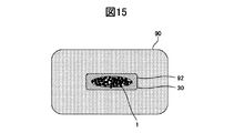
第3実施形態では、第1実施形態と同様な手順で超電導接合部100を作製した後、金属製スリーブの外周に超電導接続部100の外周に、金属スリーブ30より高い熱伝導率を持つ、高熱伝導性金属製スリーブ90を被せる工程を行う。
In the third embodiment, after producing the superconducting joint 100 in the same procedure as in the first embodiment, the outer periphery of the metal sleeve has a higher thermal conductivity than the
第1実施形態の実施例1Bで作製した超電導接続部100の電流電圧特性Aを測定した結果、図14の点線Aで示すように、実施例1Bで作製した超電導接続部100の電流電圧特性Aにおいて、クエンチ電流で急激に電圧が高くなる挙動を示すことがわかった。これは、実施例1Bで作製した超電導接続部100では、超電導フィラメント1の周囲に母材2がなくなったため、熱的に不安定になったことは要因であると考えられる。
As a result of measuring the current-voltage characteristic A of the
そこで、第3実施形態では、図15のように、超電導接続部100の外周に、金属スリーブ30より高い熱伝導率を持つ、高熱伝導性金属製スリーブ90を被せる。
Therefore, in the third embodiment, as shown in FIG. 15, a high thermal
高熱伝導性金属製スリーブ90には、常温では金属製スリーブ30を挿入できないが、高温に熱して熱膨張させたときには金属製スリーブ30が挿入できるような大きさを持つ孔92を有する。
Although the
高熱伝導性金属製スリーブ90の材料としては、金属製スリーブ30より熱膨張率が高い材質が用いられ、例えば、無酸素銅、高純度アルミニウムなどが用いられる。
As a material of the high thermal
(第3実施形態での作製方法)
第3実施形態の作製方法は、高熱伝導性金属製スリーブ90を熱し、プレスした金属製スリーブ30の外周に被せた後に徐冷する工程を行うことを除いては、第1実施形態と同じである。
(Production Method in Third Embodiment)
The manufacturing method of the third embodiment is the same as that of the first embodiment, except that the step of heating the highly heat-
第3実施形態では、高熱伝導性金属製スリーブ90を加熱し、高熱伝導性金属製スリーブ90の孔92を、プレスした金属製スリーブ30が挿入できる大きさに膨張させる。そして、高熱伝導性金属製スリーブ90を金属製スリーブ30の外周に被せ、徐冷する。これにより、高熱伝導性金属製スリーブ90は熱収縮し、金属製スリーブ30と強固に密着する。また、高熱伝導性金属製スリーブ90が内部の金属製スリーブ30及び超電導フィラメント1をさらに締め付ける効果も期待できる。
In the third embodiment, the high thermal
(実施例3A:金属製スリーブ30の外周に高熱伝導性金属製スリーブ90で被った場合)
実施例3Aでは、超電導フィラメント1の材質がニオブとチタンの合金であり、母材2の材質が銅もしくは銅合金である超電導線材10(NbTi線材)を用いた。また、低融点金属6として、スズを用い、材質がニオブである金属製スリーブ30を用いた。
(Example 3A: When the outer periphery of the
In Example 3A, a superconducting wire 10 (NbTi wire) in which the material of the
高熱伝導性金属製スリーブ90の材質として、無酸素銅を用いた。そして、高熱伝導性金属製スリーブ90の厚みは5mmとした。
Oxygen-free copper was used as the material of the high thermal
実施例3Aでの作製手順および条件は、金属製スリーブ30を加熱しながらプレスし、超電導フィラメント1の周りの低融点金属6は溶融して金属製スリーブ30の外に排出する工程までは、実施例1Bの作製手順および条件と同様である。
The manufacturing procedure and conditions in Example 3A were performed until the
実施例3Aでは、高熱伝導性金属製スリーブ90を加熱し、高熱伝導性金属製スリーブ90の孔92を、プレスした金属製スリーブ30が挿入できる大きさに膨張させた。そして、高熱伝導性金属製スリーブ90を金属製スリーブ30の外周に被せ、徐冷した。金属製スリーブ30の材質であるニオブ、および、高熱伝導性金属製スリーブ90の材質である無酸素銅、の熱膨張係数は、それぞれ常温で7.2×10⁻⁶、17.0×10⁻⁶であり、無酸素銅の方が2倍以上大きい。そのため、高熱伝導性金属製スリーブ90を液体ヘリウムもしくは冷凍機により冷却すると、高熱伝導性金属製スリーブ90を熱収縮させ、金属製スリーブ30と強固に密着させることができた。
In Example 3A, the high thermal
実施例3Aの条件で、超電導接合部100の外周に、高熱伝導性金属製スリーブ90を装着した場合の超電導接続部100のクエンチする電流を測定した。その結果、実施例1A、1Bの場合と同様に、フィラメント充填率が90%以上となったときに、超電導接続部100のクエンチ電流が向上する傾向が確認された。また、フィラメント充填率90%である超電導接続部100のクエンチ電流は、素線の臨界電流の80%以上となり、実施例1Bの場合と比較して向上することがわかった。
Under the conditions of Example 3A, the quenching current of the
そして、実施例3Aにおける超電導接続部100の電流電圧特性Bを測定した結果を図14の実線Bに示す。図14の実線Bから、クエンチ電流値において電圧値が徐序に高くなる特性になったことがわかった。これは、高熱伝導金属のスリーブ90を金属製スリーブ30の外周に装着したことにより、超電導接続部100の熱的な安定性が向上したためと考える。
And the result of having measured the current-voltage characteristic B of the
また、実施例3Aでは、金属製スリーブ30の材質をニオブとしたが、タンタル、ニオブとタンタルの複合材を用いた場合でも同様の効果があることを確認した。さらに、実施例3Aでは、高熱伝導性金属製スリーブ90の材質を無酸素銅としたが、高純度アルミニウムを用いても同様の効果があること確認した。
In Example 3A, the
以上述べたように、本発明によって、超電導フィラメントの表面に酸化膜が形成されることを抑制するとともに、鉛もしくは鉛合金を用いず環境に配慮した、超電導接続部およびその作製方法を提供することができた。 As described above, according to the present invention, it is possible to provide a superconducting connection portion and a method for manufacturing the same, which suppresses the formation of an oxide film on the surface of the superconducting filament and is environmentally friendly without using lead or a lead alloy. I was able to.
また、本発明の作製した超電導接続部は、従来の方法で作製した超電導接続部よりも、クエンチ電流が向上し、ばらつきも小さくなることがわかった。 In addition, it was found that the superconducting connection produced according to the present invention has a higher quench current and less variation than the superconducting connection produced by the conventional method.
さらに、プレスした金属製スリーブの外周に、金属製スリーブより高い熱伝導率を有する高熱伝導性金属製のスリーブを装着することにより、超電導接続部の熱的安定性を向上することができることがわかった。 Furthermore, it was found that the thermal stability of the superconducting connection can be improved by attaching a highly heat conductive metal sleeve having a higher thermal conductivity than the metal sleeve to the outer periphery of the pressed metal sleeve. It was.
100:超電導接合部、10:超電導線材、10a:超電導線材の端部、10b:未置換部、10c、10d:置換部、X:境界、1:超電導フィラメント、2:母材、6:低融点金属、A、B:超電導接続部の電流電圧特性、30:金属製スリーブ、30a:金属製スリーブの縁部、30b:金属製スリーブの端部、30c:金属製スリーブの側面、31:テーパ加工、32:金属製スリーブの孔、32e:金属製スリーブの孔の端部、90:高熱伝導性金属製のスリーブ、500:押しダイス、510:平板形状の押しダイス、520:角溝を有する押しダイス、530:丸溝を有する押しダイス、52:角溝、53:丸溝 100: Superconducting junction, 10: Superconducting wire, 10a: End of superconducting wire, 10b: Unsubstituted portion, 10c, 10d: Replaced portion, 1: Border, 1: Superconducting filament, 2: Base material, 6: Low melting point Metal, A, B: Current-voltage characteristics of superconducting connection, 30: Metal sleeve, 30a: Edge of metal sleeve, 30b: End of metal sleeve, 30c: Side surface of metal sleeve, 31: Taper processing 32: Metal sleeve hole, 32e: End of metal sleeve hole, 90: High heat conductive metal sleeve, 500: Push die, 510: Flat plate push die, 520: Push with square groove Dies, 530: Pushing dies with round grooves, 52: Square grooves, 53: Round grooves
Claims (20)
前記超電導線材の端部の母材が、鉛若しくは鉛合金を含有せず、かつ、融点が100℃以上500℃以下である低融点金属に置換されている置換部と、前記置換部を覆うための金属製スリーブとを有し、
前記金属製スリーブは、前記低融点金属の融点以上の温度で、加熱され、加熱状態で前記置換部とともに、プレスされ、
前記低融点金属の一部が前記金属製スリーブの外に排出されることによって、前記超電導フィラメント同士が密着している
ことを特徴とする超電導接続部。 A superconducting connection part connecting superconducting wires having a structure in which a superconducting filament is covered with a base material,
The base material at the end portion of the superconducting wire does not contain lead or a lead alloy, and the replacement portion is replaced with a low melting point metal having a melting point of 100 ° C. or higher and 500 ° C. or lower, and to cover the replacement portion And a metal sleeve,
The metal sleeve is heated at a temperature equal to or higher than the melting point of the low melting point metal, and is pressed together with the replacement portion in a heated state.
Wherein the Rukoto part of the low-melting metal is discharged to the outside of the metal sleeve, superconducting joint, characterized in that said superconducting filaments are in close contact.
前記超電導線材の端部がプレスされ、前記端部の母材が鉛若しくは鉛合金を含有せず、かつ、融点が100℃以上500℃以下である低融点金属に置換されている置換部と、前記置換部を覆うための金属製スリーブとを有し、
前記金属製スリーブは、前記低融点金属の融点以上の温度で、加熱され、加熱状態で前記置換部とともに、プレスされ、
前記低融点金属の一部が前記金属製スリーブの外に排出されることによって、前記超電導フィラメント同士が密着している
ことを特徴とする超電導接続部。 A superconducting connection part connecting superconducting wires having a structure in which a superconducting filament is covered with a base material,
An end portion of the superconducting wire is pressed, a base portion of the end portion does not contain lead or a lead alloy, and a replacement portion is replaced with a low melting point metal having a melting point of 100 ° C. or higher and 500 ° C. or lower; A metal sleeve for covering the replacement portion;
The metal sleeve is heated at a temperature equal to or higher than the melting point of the low melting point metal, and is pressed together with the replacement portion in a heated state.
Wherein the Rukoto part of the low-melting metal is discharged to the outside of the metal sleeve, superconducting joint, characterized in that said superconducting filaments are in close contact.
前記金属製スリーブは、前記金属製スリーブより高い熱伝導率を有する高熱伝導性金属製スリーブが被せられている
ことを特徴とする超電導接続部。 The superconducting connection part according to claim 1 or 2,
The superconducting connection part, wherein the metal sleeve is covered with a highly heat conductive metal sleeve having a higher thermal conductivity than the metal sleeve.
前記金属製スリーブの材質は、銅、ニオブ、タンタル、ニオブとタンタルの複合材のうちの少なくとも1種である
ことを特徴とする超電導接続部。 The superconducting connection part according to any one of claims 1 to 3,
A material for the metal sleeve is at least one of copper, niobium, tantalum , and a composite material of niobium and tantalum .
前記低融点金属の材質は、スズ、インジウム、スズとインジウム合金のうちの少なくとも1種である
ことを特徴とする超電導接続部。 It is a superconducting connection part of any one of Claim 1 to 4, Comprising:
The material for the low melting point metal is at least one of tin, indium , tin and an indium alloy .
前記金属製スリーブの長さは、前記置換部の長さの80%以下である
ことを特徴とする超電導接続部。 The superconducting connection part according to any one of claims 1 to 5,
The length of the metal sleeve is 80% or less of the length of the replacement part. The superconducting connection part.
前記金属製スリーブは、前記母材が前記低融点金属に置換されていない未置換部と、前記置換部と、の境界から10mm以上離れて設置されている
ことを特徴とする超電導接続部。 The superconducting connection part according to any one of claims 1 to 6,
The superconducting connection portion, wherein the metal sleeve is installed at a distance of 10 mm or more from a boundary between the non-substituted portion where the base material is not replaced with the low melting point metal and the substituted portion.
前記金属製スリーブは、
平板形状の押しダイス、角溝を有する押しダイス、丸溝を有する押しダイス、のいずれか1つを用いてプレスされている
ことを特徴とする超電導接続部。 The superconducting connection part according to any one of claims 1 to 7,
The metal sleeve is
A superconducting connection part characterized by being pressed using any one of a flat plate pressing die, a pressing die having a square groove, and a pressing die having a round groove.
前記金属スリーブがプレスされる前の前記置換部の断面形状が、長辺の長さは短辺の長さの1.5〜2.5倍である長方形になるように、前記超電導線材の端部がプレスされている
ことを特徴とする超電導接続部。 The superconducting connection part according to claim 2,
The end of the superconducting wire is such that the cross-sectional shape of the replacement part before the metal sleeve is pressed is a rectangle whose long side is 1.5 to 2.5 times the length of the short side. Superconducting connection, characterized in that the part is pressed.
前記超電導フィラメントの充填率が、90%以上であるThe filling factor of the superconducting filament is 90% or more
ことを特徴とする超電導接続部。Superconducting connection characterized by that.
鉛若しくは鉛合金を含有せず、かつ、融点が100℃以上500℃以下である低融点金属を溶融した低融点金属浴に、前記超電導線材の端部を浸漬し、前記母材を低融点金属に置換する工程と、
前記低融点金属に置換された前記超電導線材の置換部を、金属製スリーブに挿入する工程と、
前記低融点金属の融点以上の温度で、前記金属製スリーブを加熱し、加熱状態で前記置換部とともに、前記金属製スリーブをプレスし、前記低融点金属の一部を前記金属製スリーブの外に排出して前記超電導フィラメント同士を密着させる工程と、を有する
ことを特徴とする超電導接続部の作製方法。 A method for producing a superconducting connection part in which a superconducting wire having a structure in which a superconducting filament is covered with a base material is connected,
An end portion of the superconducting wire is immersed in a low melting point metal bath that does not contain lead or a lead alloy and has a melting point of 100 ° C. or more and 500 ° C. or less and melts the low melting point metal. Replacing with
Inserting the replacement portion of the superconducting wire replaced with the low melting point metal into a metal sleeve;
The metal sleeve is heated at a temperature equal to or higher than the melting point of the low melting point metal, and the metal sleeve is pressed together with the replacement portion in a heated state, and a part of the low melting point metal is placed outside the metal sleeve. And a step of discharging and bringing the superconducting filaments into close contact with each other .
前記超電導線材の端部をプレスする工程と、
鉛若しくは鉛合金を含有せず、かつ、融点が100℃以上500℃以下である低融点金属を溶融した低融点金属浴に、プレスされた前記端部を浸漬し、前記母材を低融点金属に置換する工程と、
前記低融点金属に置換された前記超電導線材の置換部を、金属製スリーブに挿入する工程と、
前記低融点金属の融点以上の温度で、前記金属製スリーブを加熱し、加熱状態で前記置換部とともに、前記金属製スリーブをプレスし、前記低融点金属の一部を前記金属製スリーブの外に排出して前記超電導フィラメント同士を密着させる工程と、を有する
ことを特徴とする超電導接続部の作製方法。 A method for producing a superconducting connection part in which a superconducting wire having a structure in which a superconducting filament is covered with a base material is connected,
Pressing the end of the superconducting wire;
The pressed end is immersed in a low-melting-point metal bath that does not contain lead or a lead alloy and has a melting point of 100 ° C. or higher and 500 ° C. or lower, and melts the low-melting-point metal. Replacing with
Inserting the replacement portion of the superconducting wire replaced with the low melting point metal into a metal sleeve;
The metal sleeve is heated at a temperature equal to or higher than the melting point of the low melting point metal, and the metal sleeve is pressed together with the replacement portion in a heated state, and a part of the low melting point metal is placed outside the metal sleeve. And a step of discharging and bringing the superconducting filaments into close contact with each other .
前記金属製スリーブより高い熱伝導率を有する高熱伝導性金属製スリーブを加熱し、プレスされた前記金属製スリーブの外周に前記高熱伝導性金属製スリーブを被せて徐冷する工程を、さらに有する
ことを特徴とする超電導接続部の作製方法。 A method of creating a superconducting connection according to claim 11 or 12 ,
The method further comprises the steps of heating a highly heat conductive metal sleeve having a higher thermal conductivity than the metal sleeve, and covering the pressed metal sleeve with the high heat conductivity metal sleeve and gradually cooling the sleeve. A method for producing a superconducting connection characterized by the above.
前記金属製スリーブの材質は、銅、ニオブ、タンタル、ニオブとタンタルの複合材のうちの少なくとも1種である
ことを特徴とする超電導接続部の作製方法。 A method for producing a superconducting connection part according to any one of claims 11 to 13 ,
A material for the metal sleeve is at least one of copper, niobium, tantalum , and a composite material of niobium and tantalum .
前記低融点金属の材質は、スズ、インジウム、スズとインジウム合金のうちの少なくとも1種である
ことを特徴とする超電導接続部の作製方法。 A method for producing a superconducting connection part according to any one of claims 11 to 14 ,
The material for the low melting point metal is at least one of tin, indium , tin and an indium alloy .
前記金属製スリーブの長さは、前記置換部の長さの80%以下である
ことを特徴とする超電導接続部の作製方法。 A method for producing a superconducting connection part according to any one of claims 11 to 15 ,
The length of the metal sleeve is 80% or less of the length of the replacement portion. A method for producing a superconducting connection portion, wherein:
前記金属製スリーブは、前記母材が前記低融点金属に置換されていない未置換部と、前記置換部と、の境界から10mm以上離れて設置されている
ことを特徴とする超電導接続部の作製方法。 A method for producing a superconducting connection part according to any one of claims 11 to 16 ,
The metal sleeve is installed at a distance of 10 mm or more from the boundary between the non-substituted portion in which the base material is not replaced with the low melting point metal and the substituted portion. Method.
平板形状の押しダイス、角溝を有する押しダイス、丸溝を有する押しダイス、のいずれか1つを用いて前記金属製スリーブのプレスを行う
ことを特徴とする超電導接続部の作製方法。 A method for producing a superconducting connection portion according to any one of claims 11 to 17 ,
The method for producing a superconducting connection part, wherein the metal sleeve is pressed using any one of a flat plate-shaped pressing die, a pressing die having a square groove, and a pressing die having a round groove.
前記金属スリーブをプレスする前の前記置換部の断面形状が、長辺の長さは短辺の長さの1.5〜2.5倍である長方形になるように、前記超電導線材の端部をプレスする
ことを特徴とする超電導接続部の作製方法。 A method for producing a superconducting connection part according to claim 12 ,
The end portion of the superconducting wire is such that the cross-sectional shape of the replacement portion before pressing the metal sleeve is a rectangle whose long side is 1.5 to 2.5 times the length of the short side. A method of manufacturing a superconducting connection, characterized by pressing
前記超電導フィラメントの充填率が、90%以上であるThe filling factor of the superconducting filament is 90% or more
ことを特徴とする超電導接続部の作製方法。A method of manufacturing a superconducting connection portion characterized by the above.
Priority Applications (1)
| Application Number | Priority Date | Filing Date | Title |
|---|---|---|---|
| JP2007333745A JP4980873B2 (en) | 2007-12-26 | 2007-12-26 | Superconducting connection part to which superconducting wire is connected and method for producing the same |
Applications Claiming Priority (1)
| Application Number | Priority Date | Filing Date | Title |
|---|---|---|---|
| JP2007333745A JP4980873B2 (en) | 2007-12-26 | 2007-12-26 | Superconducting connection part to which superconducting wire is connected and method for producing the same |
Publications (3)
| Publication Number | Publication Date |
|---|---|
| JP2009158234A JP2009158234A (en) | 2009-07-16 |
| JP2009158234A5 JP2009158234A5 (en) | 2010-02-18 |
| JP4980873B2 true JP4980873B2 (en) | 2012-07-18 |
Family
ID=40962031
Family Applications (1)
| Application Number | Title | Priority Date | Filing Date |
|---|---|---|---|
| JP2007333745A Expired - Fee Related JP4980873B2 (en) | 2007-12-26 | 2007-12-26 | Superconducting connection part to which superconducting wire is connected and method for producing the same |
Country Status (1)
| Country | Link |
|---|---|
| JP (1) | JP4980873B2 (en) |
Families Citing this family (2)
| Publication number | Priority date | Publication date | Assignee | Title |
|---|---|---|---|---|
| JP5501258B2 (en) * | 2011-01-19 | 2014-05-21 | 株式会社日立メディコ | Superconducting wire connection structure and manufacturing method thereof |
| JP5603297B2 (en) * | 2011-07-04 | 2014-10-08 | 株式会社日立製作所 | Superconducting magnet and manufacturing method thereof |
Family Cites Families (4)
| Publication number | Priority date | Publication date | Assignee | Title |
|---|---|---|---|---|
| JPS60187464U (en) * | 1984-05-22 | 1985-12-12 | 昭和電線電纜株式会社 | Superconducting wire connection |
| JPH06150993A (en) * | 1992-11-06 | 1994-05-31 | Furukawa Electric Co Ltd:The | Nbti alloy superconducting wire with connection section |
| JPH07312237A (en) * | 1994-05-16 | 1995-11-28 | Nippon Steel Corp | Connecting part of superconductive wire, and connecting method therefor |
| JP4059226B2 (en) * | 2004-04-21 | 2008-03-12 | 三菱電機株式会社 | Superconducting CIC conductor connection structure |
-
2007
- 2007-12-26 JP JP2007333745A patent/JP4980873B2/en not_active Expired - Fee Related
Also Published As
| Publication number | Publication date |
|---|---|
| JP2009158234A (en) | 2009-07-16 |
Similar Documents
| Publication | Publication Date | Title |
|---|---|---|
| US6921865B2 (en) | Superconductor connection structure | |
| US20120250726A1 (en) | Micro-thermocouple | |
| US20100245005A1 (en) | Superconducting wire rod, persistent current switch, and superconducting magnet | |
| JP6505565B2 (en) | Connection structure of high temperature superconducting conductor, high temperature superconducting coil and high temperature superconducting coil | |
| KR101112068B1 (en) | Superconducting current limiting device with magnetic field assisted quenching | |
| JP4980873B2 (en) | Superconducting connection part to which superconducting wire is connected and method for producing the same | |
| US8914087B1 (en) | Joints with very low resistance between superconducting wires and methods for making such joints | |
| JP2010015821A (en) | Precursor for manufacturing nb3sn superconductive wire rod and method of manufacturing the same, and nb3sn superconductive wire rod | |
| JP5940361B2 (en) | Superconducting current lead manufacturing method, superconducting current lead, and superconducting magnet device | |
| JP2008305765A (en) | Oxide superconductive current lead | |
| JP2005100683A (en) | Oxide superconductor energizing element | |
| JPH10106647A (en) | Wire connection structure and method for permanent current switch | |
| CN115881387A (en) | Superconducting joint, superconducting magnet, magnetic resonance imaging apparatus, and method of manufacturing superconducting joint | |
| JP3670888B2 (en) | Superconducting wire for alternating current and its manufacturing method | |
| JP2001283660A (en) | Connection structure for superconducting wire | |
| US11177588B2 (en) | High-temperature superconducting wire connection assembly | |
| JP2013089416A (en) | Superconducting wire rod, connection part of superconducting wire rod, permanent current switch, superconducting magnet system, and method of connecting superconducting wire rod | |
| JPH0982148A (en) | Cu-ni/nb-ti superconducting wire | |
| JPH10162662A (en) | Aluminum stabilized superconductor | |
| JP2003234027A (en) | Connection method and use for superconductor | |
| JP2009295296A (en) | Method for manufacturing triniobium-aluminum system compound superconductive precursor wire rod, and method for manufacturing triniobium-aluminum system compound superconductive multi-wire rod | |
| JPH06168637A (en) | Extruding billet for alternating current superconducting wire | |
| JP2006079993A (en) | MANUFACTURING METHOD OF Nb3Al SUPERCONDUCTING WIRE, AND COMPOUND WIRE MEMBER THEREFOR | |
| JP2004266141A (en) | Superconducting coil device and its manufacturing method | |
| GB2500620A (en) | Fault current limiter using ionic liquid |
Legal Events
| Date | Code | Title | Description |
|---|---|---|---|
| A521 | Written amendment |
Free format text: JAPANESE INTERMEDIATE CODE: A523 Effective date: 20091225 |
|
| A621 | Written request for application examination |
Free format text: JAPANESE INTERMEDIATE CODE: A621 Effective date: 20091225 |
|
| A977 | Report on retrieval |
Free format text: JAPANESE INTERMEDIATE CODE: A971007 Effective date: 20110914 |
|
| A131 | Notification of reasons for refusal |
Free format text: JAPANESE INTERMEDIATE CODE: A131 Effective date: 20111004 |
|
| A521 | Written amendment |
Free format text: JAPANESE INTERMEDIATE CODE: A523 Effective date: 20111130 |
|
| TRDD | Decision of grant or rejection written | ||
| A01 | Written decision to grant a patent or to grant a registration (utility model) |
Free format text: JAPANESE INTERMEDIATE CODE: A01 Effective date: 20120321 |
|
| A01 | Written decision to grant a patent or to grant a registration (utility model) |
Free format text: JAPANESE INTERMEDIATE CODE: A01 |
|
| A61 | First payment of annual fees (during grant procedure) |
Free format text: JAPANESE INTERMEDIATE CODE: A61 Effective date: 20120419 |
|
| FPAY | Renewal fee payment (event date is renewal date of database) |
Free format text: PAYMENT UNTIL: 20150427 Year of fee payment: 3 |
|
| LAPS | Cancellation because of no payment of annual fees |