JP4980002B2 - Display device - Google Patents
Display device Download PDFInfo
- Publication number
- JP4980002B2 JP4980002B2 JP2006200604A JP2006200604A JP4980002B2 JP 4980002 B2 JP4980002 B2 JP 4980002B2 JP 2006200604 A JP2006200604 A JP 2006200604A JP 2006200604 A JP2006200604 A JP 2006200604A JP 4980002 B2 JP4980002 B2 JP 4980002B2
- Authority
- JP
- Japan
- Prior art keywords
- electrode
- impurity adsorption
- adsorption electrode
- display panel
- display
- Prior art date
- Legal status (The legal status is an assumption and is not a legal conclusion. Google has not performed a legal analysis and makes no representation as to the accuracy of the status listed.)
- Active
Links
- 239000012535 impurity Substances 0.000 claims description 186
- 238000001179 sorption measurement Methods 0.000 claims description 168
- 239000004973 liquid crystal related substance Substances 0.000 claims description 118
- 239000011159 matrix material Substances 0.000 claims description 50
- 238000000034 method Methods 0.000 claims description 32
- 239000010409 thin film Substances 0.000 claims description 19
- 230000005540 biological transmission Effects 0.000 claims description 10
- 239000002245 particle Substances 0.000 claims description 4
- 230000002093 peripheral effect Effects 0.000 claims description 4
- 239000010408 film Substances 0.000 description 42
- 230000005684 electric field Effects 0.000 description 17
- 239000004065 semiconductor Substances 0.000 description 15
- 206010047571 Visual impairment Diseases 0.000 description 13
- 239000011651 chromium Substances 0.000 description 11
- 230000001681 protective effect Effects 0.000 description 11
- 230000008569 process Effects 0.000 description 10
- 239000000758 substrate Substances 0.000 description 10
- 239000000463 material Substances 0.000 description 9
- 239000004020 conductor Substances 0.000 description 8
- 238000010586 diagram Methods 0.000 description 8
- VYZAMTAEIAYCRO-UHFFFAOYSA-N Chromium Chemical compound [Cr] VYZAMTAEIAYCRO-UHFFFAOYSA-N 0.000 description 7
- 229910052804 chromium Inorganic materials 0.000 description 7
- 238000000059 patterning Methods 0.000 description 7
- 239000010949 copper Substances 0.000 description 6
- 238000004544 sputter deposition Methods 0.000 description 6
- 239000010936 titanium Substances 0.000 description 6
- 239000011368 organic material Substances 0.000 description 5
- 238000001259 photo etching Methods 0.000 description 5
- 238000005229 chemical vapour deposition Methods 0.000 description 4
- 239000003086 colorant Substances 0.000 description 4
- 230000004048 modification Effects 0.000 description 4
- 238000012986 modification Methods 0.000 description 4
- RYGMFSIKBFXOCR-UHFFFAOYSA-N Copper Chemical compound [Cu] RYGMFSIKBFXOCR-UHFFFAOYSA-N 0.000 description 3
- ZOKXTWBITQBERF-UHFFFAOYSA-N Molybdenum Chemical compound [Mo] ZOKXTWBITQBERF-UHFFFAOYSA-N 0.000 description 3
- 229910052581 Si3N4 Inorganic materials 0.000 description 3
- BQCADISMDOOEFD-UHFFFAOYSA-N Silver Chemical compound [Ag] BQCADISMDOOEFD-UHFFFAOYSA-N 0.000 description 3
- RTAQQCXQSZGOHL-UHFFFAOYSA-N Titanium Chemical compound [Ti] RTAQQCXQSZGOHL-UHFFFAOYSA-N 0.000 description 3
- 239000000956 alloy Substances 0.000 description 3
- 229910045601 alloy Inorganic materials 0.000 description 3
- 229910052782 aluminium Inorganic materials 0.000 description 3
- XAGFODPZIPBFFR-UHFFFAOYSA-N aluminium Chemical compound [Al] XAGFODPZIPBFFR-UHFFFAOYSA-N 0.000 description 3
- 230000015572 biosynthetic process Effects 0.000 description 3
- 229910052802 copper Inorganic materials 0.000 description 3
- 239000000203 mixture Substances 0.000 description 3
- 229910052750 molybdenum Inorganic materials 0.000 description 3
- 239000011733 molybdenum Substances 0.000 description 3
- HQVNEWCFYHHQES-UHFFFAOYSA-N silicon nitride Chemical compound N12[Si]34N5[Si]62N3[Si]51N64 HQVNEWCFYHHQES-UHFFFAOYSA-N 0.000 description 3
- 229910052709 silver Inorganic materials 0.000 description 3
- 239000004332 silver Substances 0.000 description 3
- 229910052715 tantalum Inorganic materials 0.000 description 3
- GUVRBAGPIYLISA-UHFFFAOYSA-N tantalum atom Chemical compound [Ta] GUVRBAGPIYLISA-UHFFFAOYSA-N 0.000 description 3
- 229910052719 titanium Inorganic materials 0.000 description 3
- VYPSYNLAJGMNEJ-UHFFFAOYSA-N Silicium dioxide Chemical compound O=[Si]=O VYPSYNLAJGMNEJ-UHFFFAOYSA-N 0.000 description 2
- 229910021417 amorphous silicon Inorganic materials 0.000 description 2
- 230000000295 complement effect Effects 0.000 description 2
- 238000005530 etching Methods 0.000 description 2
- 229910052751 metal Inorganic materials 0.000 description 2
- 239000002184 metal Substances 0.000 description 2
- 229920002120 photoresistant polymer Polymers 0.000 description 2
- 238000000623 plasma-assisted chemical vapour deposition Methods 0.000 description 2
- 229920001721 polyimide Polymers 0.000 description 2
- 238000005546 reactive sputtering Methods 0.000 description 2
- 229910052814 silicon oxide Inorganic materials 0.000 description 2
- 239000004925 Acrylic resin Substances 0.000 description 1
- 229920000178 Acrylic resin Polymers 0.000 description 1
- 206010034972 Photosensitivity reaction Diseases 0.000 description 1
- 239000004642 Polyimide Substances 0.000 description 1
- 229910004205 SiNX Inorganic materials 0.000 description 1
- 230000004888 barrier function Effects 0.000 description 1
- 239000006229 carbon black Substances 0.000 description 1
- 230000008859 change Effects 0.000 description 1
- 238000005352 clarification Methods 0.000 description 1
- 239000000470 constituent Substances 0.000 description 1
- 230000003247 decreasing effect Effects 0.000 description 1
- 230000006866 deterioration Effects 0.000 description 1
- 238000009792 diffusion process Methods 0.000 description 1
- 239000003822 epoxy resin Substances 0.000 description 1
- 239000012530 fluid Substances 0.000 description 1
- AMGQUBHHOARCQH-UHFFFAOYSA-N indium;oxotin Chemical compound [In].[Sn]=O AMGQUBHHOARCQH-UHFFFAOYSA-N 0.000 description 1
- 229910010272 inorganic material Inorganic materials 0.000 description 1
- 239000011147 inorganic material Substances 0.000 description 1
- 150000002500 ions Chemical class 0.000 description 1
- 239000007788 liquid Substances 0.000 description 1
- 230000014759 maintenance of location Effects 0.000 description 1
- 150000004767 nitrides Chemical class 0.000 description 1
- 230000003287 optical effect Effects 0.000 description 1
- 238000005192 partition Methods 0.000 description 1
- 230000036211 photosensitivity Effects 0.000 description 1
- 229920000647 polyepoxide Polymers 0.000 description 1
- 239000009719 polyimide resin Substances 0.000 description 1
- 239000000047 product Substances 0.000 description 1
- 238000000926 separation method Methods 0.000 description 1
- 238000004528 spin coating Methods 0.000 description 1
- 239000000126 substance Substances 0.000 description 1
- 239000013589 supplement Substances 0.000 description 1
- 230000001629 suppression Effects 0.000 description 1
- 229920001187 thermosetting polymer Polymers 0.000 description 1
- YVTHLONGBIQYBO-UHFFFAOYSA-N zinc indium(3+) oxygen(2-) Chemical compound [O--].[Zn++].[In+3] YVTHLONGBIQYBO-UHFFFAOYSA-N 0.000 description 1
Images


Classifications
-
- G—PHYSICS
- G02—OPTICS
- G02F—OPTICAL DEVICES OR ARRANGEMENTS FOR THE CONTROL OF LIGHT BY MODIFICATION OF THE OPTICAL PROPERTIES OF THE MEDIA OF THE ELEMENTS INVOLVED THEREIN; NON-LINEAR OPTICS; FREQUENCY-CHANGING OF LIGHT; OPTICAL LOGIC ELEMENTS; OPTICAL ANALOGUE/DIGITAL CONVERTERS
- G02F1/00—Devices or arrangements for the control of the intensity, colour, phase, polarisation or direction of light arriving from an independent light source, e.g. switching, gating or modulating; Non-linear optics
- G02F1/01—Devices or arrangements for the control of the intensity, colour, phase, polarisation or direction of light arriving from an independent light source, e.g. switching, gating or modulating; Non-linear optics for the control of the intensity, phase, polarisation or colour
- G02F1/13—Devices or arrangements for the control of the intensity, colour, phase, polarisation or direction of light arriving from an independent light source, e.g. switching, gating or modulating; Non-linear optics for the control of the intensity, phase, polarisation or colour based on liquid crystals, e.g. single liquid crystal display cells
- G02F1/133—Constructional arrangements; Operation of liquid crystal cells; Circuit arrangements
- G02F1/1333—Constructional arrangements; Manufacturing methods
- G02F1/1335—Structural association of cells with optical devices, e.g. polarisers or reflectors
- G02F1/133502—Antiglare, refractive index matching layers
-
- G—PHYSICS
- G02—OPTICS
- G02F—OPTICAL DEVICES OR ARRANGEMENTS FOR THE CONTROL OF LIGHT BY MODIFICATION OF THE OPTICAL PROPERTIES OF THE MEDIA OF THE ELEMENTS INVOLVED THEREIN; NON-LINEAR OPTICS; FREQUENCY-CHANGING OF LIGHT; OPTICAL LOGIC ELEMENTS; OPTICAL ANALOGUE/DIGITAL CONVERTERS
- G02F1/00—Devices or arrangements for the control of the intensity, colour, phase, polarisation or direction of light arriving from an independent light source, e.g. switching, gating or modulating; Non-linear optics
- G02F1/01—Devices or arrangements for the control of the intensity, colour, phase, polarisation or direction of light arriving from an independent light source, e.g. switching, gating or modulating; Non-linear optics for the control of the intensity, phase, polarisation or colour
- G02F1/13—Devices or arrangements for the control of the intensity, colour, phase, polarisation or direction of light arriving from an independent light source, e.g. switching, gating or modulating; Non-linear optics for the control of the intensity, phase, polarisation or colour based on liquid crystals, e.g. single liquid crystal display cells
- G02F1/133—Constructional arrangements; Operation of liquid crystal cells; Circuit arrangements
- G02F1/1333—Constructional arrangements; Manufacturing methods
- G02F1/1335—Structural association of cells with optical devices, e.g. polarisers or reflectors
-
- G—PHYSICS
- G02—OPTICS
- G02F—OPTICAL DEVICES OR ARRANGEMENTS FOR THE CONTROL OF LIGHT BY MODIFICATION OF THE OPTICAL PROPERTIES OF THE MEDIA OF THE ELEMENTS INVOLVED THEREIN; NON-LINEAR OPTICS; FREQUENCY-CHANGING OF LIGHT; OPTICAL LOGIC ELEMENTS; OPTICAL ANALOGUE/DIGITAL CONVERTERS
- G02F1/00—Devices or arrangements for the control of the intensity, colour, phase, polarisation or direction of light arriving from an independent light source, e.g. switching, gating or modulating; Non-linear optics
- G02F1/01—Devices or arrangements for the control of the intensity, colour, phase, polarisation or direction of light arriving from an independent light source, e.g. switching, gating or modulating; Non-linear optics for the control of the intensity, phase, polarisation or colour
- G02F1/13—Devices or arrangements for the control of the intensity, colour, phase, polarisation or direction of light arriving from an independent light source, e.g. switching, gating or modulating; Non-linear optics for the control of the intensity, phase, polarisation or colour based on liquid crystals, e.g. single liquid crystal display cells
- G02F1/133—Constructional arrangements; Operation of liquid crystal cells; Circuit arrangements
- G02F1/1333—Constructional arrangements; Manufacturing methods
- G02F1/133388—Constructional arrangements; Manufacturing methods with constructional differences between the display region and the peripheral region
-
- G—PHYSICS
- G02—OPTICS
- G02F—OPTICAL DEVICES OR ARRANGEMENTS FOR THE CONTROL OF LIGHT BY MODIFICATION OF THE OPTICAL PROPERTIES OF THE MEDIA OF THE ELEMENTS INVOLVED THEREIN; NON-LINEAR OPTICS; FREQUENCY-CHANGING OF LIGHT; OPTICAL LOGIC ELEMENTS; OPTICAL ANALOGUE/DIGITAL CONVERTERS
- G02F1/00—Devices or arrangements for the control of the intensity, colour, phase, polarisation or direction of light arriving from an independent light source, e.g. switching, gating or modulating; Non-linear optics
- G02F1/01—Devices or arrangements for the control of the intensity, colour, phase, polarisation or direction of light arriving from an independent light source, e.g. switching, gating or modulating; Non-linear optics for the control of the intensity, phase, polarisation or colour
- G02F1/13—Devices or arrangements for the control of the intensity, colour, phase, polarisation or direction of light arriving from an independent light source, e.g. switching, gating or modulating; Non-linear optics for the control of the intensity, phase, polarisation or colour based on liquid crystals, e.g. single liquid crystal display cells
- G02F1/133—Constructional arrangements; Operation of liquid crystal cells; Circuit arrangements
- G02F1/1333—Constructional arrangements; Manufacturing methods
- G02F1/133397—Constructional arrangements; Manufacturing methods for suppressing after-image or image-sticking
Description
本発明は、表示装置に関し、より詳しくは、表示画面の残像現象が抑制された表示装置に関する。 The present invention relates to a display device, and more particularly to a display device in which an afterimage phenomenon of a display screen is suppressed.
液晶表示装置(Liquid Crystal Display;LCD)は、現在最も広く使用されている平板表示装置(Flat Panel Display)のうち一つである。液晶表示装置は、電極が形成されている二枚の表示板と、それらの間に挟持されている液晶層とを有している。液晶層は、光学的異方性及び誘電率異方性を有する液晶分子から構成される。表示板の電極に電圧を印加することによって液晶層に電界が生成されるようになれば、液晶層を構成する液晶分子が再配列し、液晶層を透過する光量が調節される。 The liquid crystal display (LCD) is one of the most widely used flat panel displays (Flat Panel Display). The liquid crystal display device has two display panels on which electrodes are formed, and a liquid crystal layer sandwiched between them. The liquid crystal layer is composed of liquid crystal molecules having optical anisotropy and dielectric anisotropy. When an electric field is generated in the liquid crystal layer by applying a voltage to the electrodes of the display panel, the liquid crystal molecules constituting the liquid crystal layer are rearranged, and the amount of light transmitted through the liquid crystal layer is adjusted.
ところで、液晶分子に同一極性の電圧が印加され続ける場合、液晶分子が劣化し、液晶層に直流バイアスが累積されて残留するようになる。このように残留した直流バイアスは、その後に印加されるデータ電圧を変形させるか、或いはデータ電圧が供給されない場合にも望まない電界を液晶層内に生成させてしまう。このような液晶分子の劣化を防止するため、液晶層に印加される電圧の極性を反転させる反転駆動法が開発された。反転駆動としては、フレーム反転、ライン反転、ドット反転などの方法が用いられている。しかしながら、これら反転駆動を行っても、様々な理由によるキックバック電圧の変化などによって液晶層には直流バイアスが残留するようになる。 By the way, when a voltage of the same polarity is continuously applied to the liquid crystal molecules, the liquid crystal molecules are deteriorated, and a DC bias is accumulated in the liquid crystal layer and remains. The DC bias remaining in this manner deforms the data voltage applied thereafter, or generates an undesired electric field in the liquid crystal layer even when the data voltage is not supplied. In order to prevent such deterioration of the liquid crystal molecules, an inversion driving method has been developed in which the polarity of the voltage applied to the liquid crystal layer is inverted. As inversion driving, methods such as frame inversion, line inversion, and dot inversion are used. However, even if these inversion drives are performed, a DC bias remains in the liquid crystal layer due to a change in kickback voltage due to various reasons.
一方、液晶層内には、液晶分子以外にイオン性不純物が浮遊するが、このようなイオン性不純物は液晶層に累積した直流バイアスによって表示板の電極に吸着する。このように吸着したイオン性不純物は、液晶層に生成される電界を歪曲させるようになる。これは表示画面上では残像として視認されるようになる。
本発明が解決しようとする技術的課題は、残像現象が改善された表示装置を提供することにある。 The technical problem to be solved by the present invention is to provide a display device with improved afterimage phenomenon.
本発明が解決しようとする他の技術的課題は、前記表示装置の駆動方法を提供することにある。 Another technical problem to be solved by the present invention is to provide a method for driving the display device.
本発明の技術的課題は、以上で言及した技術的課題に制限されるわけではなく、言及されない又は他の技術的課題は、以下の記載から当業者に明確に理解される。 The technical problems of the present invention are not limited to the technical problems mentioned above, and other technical problems not mentioned or other technical problems will be clearly understood by those skilled in the art from the following description.
前記技術的課題を達成するための本発明の一実施形態による表示装置は、第1の方向に平行に延びている複数のゲート線と、第2の方向に平行に延びている複数のデータ線と、透過領域に形成された画素電極、及び遮光領域に形成され、前記画素電極と分離され、前記ゲート線及び前記データ線と絶縁されて重畳して形成される第1の不純物吸着電極を含む第1の表示板と、前記第1の不純物吸着電極と対向する前記遮光領域に形成された第2の不純物吸着電極を含み、前記第1の表示板に対向する第2の表示板と、前記第1及び第2の表示板との間に介在する媒体とを含む。 In order to achieve the above technical problem, a display device according to an embodiment of the present invention includes a plurality of gate lines extending in parallel to a first direction and a plurality of data lines extending in parallel to a second direction. And a pixel electrode formed in the transmissive region and a first impurity adsorption electrode formed in the light shielding region, separated from the pixel electrode, and formed to be insulated and overlapped with the gate line and the data line. A first display panel that includes the second impurity adsorption electrode formed in the light-shielding region facing the first impurity adsorption electrode, the second display panel facing the first display panel, And a medium interposed between the first and second display panels.
前記技術的課題を達成するための本発明の他の実施形態による表示装置は、表示領域の最外郭周縁に形成され、画素電極と分離されている第1の不純物吸着電極を含む第1の表示板と、前記第1の不純物吸着電極と対向する第2の不純物吸着電極を含み、前記第1の表示板に対向する第2の表示板と、前記第1及び第2の表示板との間に介在する媒体とを含み、前記第1の不純物吸着電極は、画素毎に形成されたそれぞれの薄膜トランジスタの制御端子に接続されたゲート線及び前記薄膜トランジスタの入力端子に接続されたデータ線と絶縁されて重畳するように表示領域内側に延長された吸着電極領域をさらに含み、
前記第2の不純物吸着電極は、前記第1の不純物吸着電極に対向するように表示領域の内側に延長された吸着電極領域をさらに含む。
A display device according to another embodiment of the present invention for achieving the above technical problem includes a first display including a first impurity adsorption electrode formed at an outermost peripheral edge of a display region and separated from a pixel electrode. A plate, a second impurity adsorption electrode facing the first impurity adsorption electrode, and a second display panel opposed to the first display panel, and the first and second display plates look containing a medium interposed, said first impurity adsorption electrode is insulated from the data lines connected to the input terminal of each of the connected gate line and the thin film transistor to the control terminal of the TFT formed in each pixel A suction electrode region extended inside the display region so as to overlap,
It said second impurity adsorption electrode further including a suction electrode region which extends inside the display region so as to face the first impurity adsorption electrode.
前記技術的課題を達成するための本発明のさらに他の実施形態による表示装置は、画素毎に形成されたそれぞれの薄膜トランジスタの制御端子に接続されたゲート線、前記薄膜トランジスタの入力端子に接続されたデータ線、前記薄膜トランジスタの出力端子に接続された画素電極、及び前記ゲート線及び前記データ線と絶縁されて重畳して形成され、前記画素電極と分離された第1の不純物吸着電極を備える第1の表示板と、格子状のブラックマトリクスパターン、及び、前記ブラックマトリクスパターン下に重畳されて形成された前記第1の不純物吸着電極と対向する第2の不純物吸着電極を含み、前記第1の表示板に対向する第2の表示板と、前記第1及び第2の表示板との間に介在する液晶層とを含む。 The display device according to another embodiment of the present invention for achieving the technical problem is connected to a gate line connected to a control terminal of each thin film transistor formed for each pixel and to an input terminal of the thin film transistor. data line, a pixel electrode connected to an output terminal of the thin film transistor, and is formed by overlapping are insulated from the gate line及beauty before Symbol data lines, comprising a first impurity adsorption electrode which is separated from the pixel electrode A first display panel, a grid-like black matrix pattern, and a second impurity adsorption electrode opposed to the first impurity adsorption electrode formed to overlap the black matrix pattern; A second display panel facing the display panel, and a liquid crystal layer interposed between the first and second display panels.
前記他の技術的課題を達成するための本発明の一実施形態による表示装置の駆動方法は、
第1の方向に平行に延びている複数のゲート線と、第2の方向に平行に延びている複数のデータ線と、透過領域に形成された画素電極と、遮光領域に形成され、前記画素電極と分離され、前記ゲート線及び前記データ線と絶縁されて重畳して形成される第1の不純物吸着電極を含む第1の表示板と、前記第1の不純物吸着電極と対向する前記遮光領域に形成された第2の不純物吸着電極を含み、前記第1の表示板に対向する第2の表示板と、前記第1及び第2の表示板との間に介在する媒介とを含む前記表示装置の駆動方法であって、前記第1の不純物吸着電極に第1の電圧を印加する段階と、前記第2の不純物吸着電極に第2の電圧を印加する段階と、前記第1の不純物吸着電極と前記第2の不純物吸着電極とに前記第1及び第2の不純物吸着電極間平均電位差の絶対値が前記媒体の透過領域に残留するDCバイアスの絶対値より大きいように電圧を印加することを含む。
A method of driving a display device according to an embodiment of the present invention to achieve the other technical problem is as follows.
A plurality of gate lines extending in parallel to the first direction; a plurality of data lines extending in parallel to the second direction; a pixel electrode formed in a transmissive region; A first display panel including a first impurity adsorption electrode which is separated from an electrode and is formed so as to be insulated and overlapped with the gate line and the data line; and the light shielding region facing the first impurity adsorption electrode It includes a second impurity adsorption electrode formed on a second display panel facing the first display panel, before Symbol including the intermediary interposed between the first and second display panel a method of driving a Viewing device, applying a first voltage to the first impurity adsorption electrode, applying a second voltage to said second impurity adsorption electrode, the first The first and second impurities are included in the impurity adsorption electrode and the second impurity adsorption electrode. The absolute value of the average difference between Chakudenkyoku comprises applying a voltage to be greater than the absolute value of the DC bias remaining in the transmissive region of the medium.
その他実施形態の具体的な事項は、詳細な説明及び図面に含まれている。 Specific matters of the other embodiments are included in the detailed description and the drawings.
本発明の実施形態に係る液晶表示装置によれば、遮光領域上に不純物吸着電極を形成し、ここに画素領域の残留DCバイアスより大きい電位差が形成されるように外部電圧を印加することによって、画素領域に浮遊する不純物イオンを吸着することができる。従って、画素領域内のイオン性不純物の量が減少することになり、残像現象を抑制することができる。 According to the liquid crystal display device according to the embodiment of the present invention, the impurity adsorption electrode is formed on the light shielding region, and an external voltage is applied thereto so that a potential difference larger than the residual DC bias of the pixel region is formed. Impurity ions floating in the pixel region can be adsorbed. Therefore, the amount of ionic impurities in the pixel region is reduced, and the afterimage phenomenon can be suppressed.
本発明の利点、特徴及びそれらを達成する方法は、添付する図面と共に詳細に説明している実施形態を参照すれば明確になる。しかしながら、本発明は、以下で開示される実施形態に限定されるわけではなく、相異なる多様な形態で実現され得る。本実施形態は、本発明の開示が完全となり、当業者に発明の範疇を完全に知らせるために提供されるに過ぎず、本発明は、特許請求の範囲の記載に基づいて解釈されなければならない。なお、明細書全体にかけて同一参照符号は同一構成要素を示すものとする。図面において、層、領域の大きさ及びこれらの相対的な大きさは、説明の便宜上誇張されている場合がある。 The advantages, features and methods of achieving the same of the present invention will become apparent with reference to the embodiments described in detail in conjunction with the accompanying drawings. However, the present invention is not limited to the embodiments disclosed below, and can be realized in various different forms. The embodiments are provided only for the complete disclosure of the present invention and to fully inform those skilled in the art of the scope of the invention, and the present invention should be construed based on the claims. . Note that the same reference numerals denote the same components throughout the specification. In the drawings, the sizes of layers and regions and their relative sizes may be exaggerated for convenience of explanation.
空間的に相対的な用語である「下(below)」、「下方(beneath)」、「下部(lower)」、「上(above)」、「上部(upper)」などは、図面に示すように一つの素子又は構成要素と他の素子又は構成要素との相間関係を容易に記述するため用いられている。空間的に相対的な用語は、図面に示す方向に加えて使用時又は動作時素子の相異なる方向を含む用語に理解されなければならない。例えば、図面に示す素子をひっくり返す場合、他の素子の「下(below)又は下方(beneath)」に図示されている素子は、他の素子の「上(above)」に配置されていることになる。従って、例示的な用語である「下(below)又は下方(beneath)」は、上下方向を全て含んでいるということができる。素子は、他の方向にも配列させることができ、この場合、空間的に相対的な用語は配列によって解釈することができる。 The spatially relative terms “below”, “beneath”, “lower”, “above”, “upper” and the like are shown in the drawings. Are used to easily describe the interrelationship between one element or component and another element or component. Spatial relative terms should be understood to include different directions of the element in use or in operation in addition to the directions shown in the drawings. For example, if the element shown in the drawing is turned over, the element shown “below” or “beneath” of another element is arranged “above” the other element. Become. Accordingly, it can be said that the exemplary term “below” or “beneath” includes all the vertical directions. The elements can also be arranged in other directions, in which case spatially relative terms can be interpreted by the arrangement.
以下、添付した図面を参照して本発明の好ましい実施形態による表示装置について詳細に説明する。以下では本発明の実施形態による表示装置として液晶表示装置が例示されているが、これに限定されるわけではない。 Hereinafter, a display device according to a preferred embodiment of the present invention will be described in detail with reference to the accompanying drawings. Hereinafter, a liquid crystal display device is illustrated as a display device according to an embodiment of the present invention, but the present invention is not limited to this.
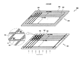
図1は、本発明の一実施形態による液晶表示装置の概略分解斜視図である。 FIG. 1 is a schematic exploded perspective view of a liquid crystal display device according to an embodiment of the present invention.
図1を参照する。液晶表示装置500は、第1の表示板100、第1の表示板100に対向する第2の表示板200及びこれらの間に介在する媒体を含む。ここで、液晶表示装置の媒体は、液晶を含む液晶層であるようにしてもよい。本明細書において、第1の表示板100、第2の表示板200及び液晶層からなるパネルを「液晶パネル」と称する場合がある。
Please refer to FIG. The liquid
第1の表示板100は、第1の方向に平行に延びている多数本のゲート線122及び第2の方向に平行に延びている多数本のデータ線162を含む。ゲート線122とデータ線162とは導電性物質からなる。ゲート線122とデータ線162とは、例えば、アルミニウム(Al)、銅(Cu)、銀(Ag)、モリブデン(Mo)、クロム(Cr)、チタン(Ti)、タンタル(Ta)又はこれらの合金などからなり、単一膜又は2層以上の多層膜からなるようにしてもよい。ゲート線122とデータ線162とは、互いに交差するよう形成されており、例えば、垂直に交差するようにしてもよい。隣接するゲート線122と隣接するデータ線162とは、それぞれ互いに交差しながら一つの画素を定義する。それぞれの画素には薄膜トランジスタ(Q)及びそれによってスイッチングされる画素電極182が備えられている。
The
第2の表示板200は、格子状に形成されたブラックマトリクスパターン220及びカラーフィルタパターン230を含む。ブラックマトリクスパターン220は、不透明な物質からなり、画素の境界に沿って形成される。カラーフィルタパターン230は、例えば、赤色(R)、緑色(G)、青色(B)のカラーフィルタが交代に配置されている。それぞれのカラーフィルタパターン230は、ブラックマトリクスパターン220によって取り囲まれている。本実施形態の変形例としては、それぞれのカラーフィルタパターン230が上述した配列とは異なる配列、例えば、赤色(R)、緑色(G)、青色(B)のそれぞれの補色に相当するカラーフィルタパターン230を使用した配列としてもよいが、これに限定されるわけではない。カラーフィルタパターン230は、ブラックマトリクスパターン220と共に表示領域を構成する。第2の表示板200の最外郭周縁には最外郭ブラックマトリクス225が形成されており、非表示領域を構成する。以下単に「ブラックマトリクス」と表現される場合は、表示領域内のブラックマトリクスパターン220だけではなく最外郭ブラックマトリクス225を含んでいる場合がある。
The
最外郭ブラックマトリクス225は、表示領域内のブラックマトリクスパターン220と同一物質からなるが、表示領域内のブラックマトリクスパターン220より広い幅を有するようにしてもよい。すなわち、ブラックマトリクス220、225の幅は、適用される液晶表示装置の大きさ、画素数などによって異なる。例えば、表示領域内のブラックマトリクスパターン220は、約30μm〜40μm程度の幅を有している。一方、最外郭ブラックマトリクス225は、0.5mm〜50mmの幅を有するようにしてもよい。
The outermost
第1の表示板100と第2の表示板200とは、液晶層を媒体として介在させ、互いに貼り合わせられている。なお、第1の表示板100のゲート線122及びデータ線162は、第2の表示板200のブラックマトリクス220、225と重畳するように配置される。図1において第1の表示板100上に示されている点線は、第1の表示板100と第2の表示板200とを配置する場合の最外郭ブラックマトリクス225内側線の透視線であり、表示領域と非表示領域との境界に相当する。
The
一方、第1の表示板100の下には、バックライトアセンブリが配置される。バックライトアセンブリから出射された光は、第1の表示板100、液層層及び第2の表示板200を経て伝搬する。
Meanwhile, a backlight assembly is disposed under the
ここで、第1の表示板100のゲート線122とデータ線162とは、低抵抗配線を具現するため導電性物質、その中でも主に不透明な導電性物質からなるので、バックライトアセンブリから出射された光の大部分を遮光する。一方、画素の大部分を占める画素電極182は、酸化インジウム錫(Indium Tin Oxide;ITO)や酸化インジウム亜鉛(Indium Zinc Oxide;IZO)のような透明な導電性物質からなるので、バックライトアセンブリから出射された光の大部分が透過する。液晶層においては、液晶分子の配列方向に沿って光が透過したり、遮光されたりする。液晶の配列は、液晶層内に形成される電界の強度によって制御される。第2の表示板200のブラックマトリクス220、225は透過した光を遮光する。一方、第2の表示板200のカラーフィルタパターン230は光を透過させる。
Here, since the
上述したようにバックライトアセンブリから出射された光は、第1の表示板100、液晶層及び第2の表示板200のうち少なくともいずれか一つに遮光されることによって液晶パネルを通過できないようになる。液晶層における遮光の程度は、液晶層に生成される電界によって変化する。そこで、電界と関係なく光が遮光される領域を「遮光領域」と定義するとき、遮光領域は第1の表示板の遮光領域と第2の表示板の遮光領域との和集合になる。また、液晶パネルの遮光領域以外の領域、すなわち電界によって光の透過が制御される領域を「透過領域」と定義する。
As described above, the light emitted from the backlight assembly is blocked by at least one of the
図2は、本発明の一実施形態による液晶表示装置の平面図である。図2において、点線は、液晶表示装置500の第1の表示板に形成されたゲート線122、データ線162及び画素電極182を示す。
FIG. 2 is a plan view of a liquid crystal display device according to an embodiment of the present invention. In FIG. 2, dotted lines indicate the
図2を参照する。遮光領域は、第1の表示板のゲート線122及びデータ線162と第2の表示板のブラックマトリクスパターン220とが形成された領域の和集合になる。また、遮光領域は表示領域内側だけではなく、最外郭ブラックマトリクス225が配置されている非表示領域も含んでいる。
Please refer to FIG. The light shielding area is a union of areas where the
表示領域内側の第2の表示板のブラックマトリクスパターン220は、遮光領域を最小化するために第1の表示板のゲート線122及びデータ線162と重畳して配置されている。また、ブラックマトリクスパターン220の幅は、光リーク現象を防止し視認性をよくするためにゲート線122及びデータ162線より広く形成されている。すなわち、上から見ると、ブラックマトリクスパターン220がゲート線122及びデータ線162を覆うように形成されている。
The
一方、透過領域は、第1の表示板の画素電極182と第2の表示板のカラーフィルタパターン230領域との積集合に相当する。カラーフィルタパターン230は、画素電極182の内部に重畳されて形成するようにしてもよい。
On the other hand, the transmission region corresponds to a product set of the
以下、上述した本発明の一実施形態による液晶表示装置の画素単位についてさらに詳細に説明する。 Hereinafter, the pixel unit of the liquid crystal display device according to the embodiment of the present invention will be described in more detail.
図3Aは、本発明の一実施形態による第1の表示板のレイアウト図である。図3Bは、図3AのIIIb−IIIb´線に沿った断面図である。図面の明確化と説明の便宜上、図3Aのレイアウト図においては第1の表示板の一部構成要素が省略されている。 FIG. 3A is a layout diagram of a first display panel according to an exemplary embodiment of the present invention. 3B is a cross-sectional view taken along line IIIb-IIIb ′ of FIG. 3A. For the sake of clarification and explanation, some components of the first display panel are omitted in the layout diagram of FIG. 3A.
図3A及び図3Bを参照する。絶縁基板110上にゲート信号を伝達する複数のゲート配線122、124、126が形成されている。ゲート配線は、第1の方向(図3Aでは横方向)に延びているゲート線122、ゲート線122の端部に接続されており、外部からゲート信号が印加されてゲート線122に伝達するゲートパッド124、及びゲート線122に接続されて突起形態に形成された薄膜トランジスタのゲート電極126を含む。ゲート配線122、124、126は、これに限定されるわけではないが、アルミニウム(Al)、銅(Cu)、銀(Ag)、モリブデン(Mo)、クロム(Cr)、チタン(Ti)、タンタル(Ta)又はこれらの合金などからなるようにしてもよく、これらの物質をスパッタリングなどの方法で絶縁基板110上に形成した後、フォトエッチング工程によってパターニングすることによって形成するようにしてもよい。
Please refer to FIG. 3A and FIG. 3B. A plurality of
また、ゲート配線122、124、126は、必要に応じて2層以上に構成された多層膜として形成されるようにしてもよい。例えば、絶縁基板110との接着性を改善し、また、バリア膜として機能する下部膜と、低抵抗導電層及び前記低抵抗導電層構成物質の拡散を防ぎ、キャッピング膜として機能する上部膜とから構成するようにしてもよい。ゲート配線122、124、126は、一例として、Mo/Al/Mo三重膜構造を挙げることができる。また、下部膜や上部膜の材質としては導電性酸化物又は窒化物を用いるようにしてもよい。ゲート配線122、124、126は、一例として、ITO/Ag/ITO三重膜構造を挙げることができる。
Further, the
一方、図面の明確化と説明の便宜上、示さないが、絶縁基板110のゲート配線122、124、126と同一な層には画素の電荷保持能力を向上させるストレージ電極をさらに形成するようにしてもよい。ストレージ電極は、ゲート配線122、124、126と同一な物質からなり、ゲート配線122、124、126と同時に形成及びパターニングすることができる。ストレージ電極の形及び配置などは多様な形態に変形することができ、画素電極182とゲート線122との重畳などによって発生するストレージ容量が十分である場合は、形成されない場合もある。
On the other hand, although not shown for the sake of clarity of the drawings and explanation, a storage electrode for improving the charge retention capability of the pixel may be further formed in the same layer as the
ゲート配線122、124、126が形成された絶縁基板の全面は、ゲート絶縁膜130に覆われている。ゲート絶縁膜130は、窒化シリコン(SiNx)などからなり、例えば、スパッタリング、反応性スパッタリング、化学気相成長(Chemical Vapor Deposition;CVD)などの方法で形成される。
The entire surface of the insulating substrate on which the
ゲート絶縁膜130上には、ゲート電極126と少なくとも一部が重畳する半導体層140が形成されている。半導体層140は、水素化非晶質シリコンなどの半導体からなる。半導体層140の上には、オーミックコンタクト層155、156が形成されている。オーミックコンタクト層155、156は、n型不純物が高濃度にドーピングされたn+水素化非晶質シリコンなどからなる。オーミックコンタクト層155、156は全体的に半導体層140を覆っているが、半導体層140を中心に分離されて半導体層140の一部を露出する。オーミックコンタクト層155、156の一部はゲート絶縁膜130と直接コンタクトしている。
A
半導体層140及びオーミックコンタクト層155、156は、例えば、CVD方法によって形成され、フォトエッチング工程によってパターニングされる。選択されるマスク工程によっては、島状に形成されるか、或いは線状に形成されるようにしてもよい。島状に形成される場合、オーミックコンタクト層155、156の分離パターンを除いては、後述するデータ配線の形成前に先ずパターニングするようにしてもよい。
The
オーミックコンタクト層155、156及びゲート絶縁膜130上には、データ配線162、165、166、168が形成されている。データ配線はデータ信号を伝達し、第2の方向(図1Aでは縦方向)に形成されているデータ線162、データ線162の分枝であり、オーミックコンタクト層155の上部まで延長されているソース電極165、データ線162の一側端部に接続されている。データ配線は、外部からの画像信号が印加されるデータパッド168、ソース電極165と分離されており、ゲート電極126又は薄膜トランジスタのチャネル部についてソース電極165の反対側オーミックコンタクト層156上部に形成されているドレイン電極166を含む。
データ線162は、ゲート線122とゲート絶縁膜130とによって絶縁されて交差し、隣接するデータ線162及び隣接するゲート線122の交差によって形成された領域が一つの画素を構成するようになる。
The
このようなデータ配線162、165、166、168は、これらに限定されるわけではないが、アルミニウム(Al)、銅(Cu)、銀(Ag)、モリブデン(Mo)、クロム(Cr)、チタン(Ti)、タンタル(Ta)又はこれらの合金などからなるようにしてもよく、前記物質をスパッタリングなどの方法で絶縁基板110上に形成した後、フォトエッチング工程によってパターニングされる。選択されるマスク工程によっては、下部のオーミックコンタクト層155、156及び半導体層140と別のフォトレジストマスクをエッチングマスクとして用いてデータ配線をパターニングするようにしてもよい。
Such data wirings 162, 165, 166, 168 are not limited to these, but are aluminum (Al), copper (Cu), silver (Ag), molybdenum (Mo), chromium (Cr), titanium. It may be made of (Ti), tantalum (Ta), or an alloy thereof, and after the material is formed on the insulating
データ配線162、165、166、168は、必要に応じて2層以上に構成された多層膜として形成することができるが、上述したゲート配線122、124、126の形成と同様であるので、ここでは重複説明は省略する。
The data wirings 162, 165, 166, and 168 can be formed as a multilayer film having two or more layers as necessary, but are the same as the formation of the
上述したようなゲート電極126、その上に形成された半導体層140、オーミックコンタクト層155、156並びにソース電極165及びドレイン電極166は、薄膜トランジスタを構成する。ここで、ゲート電極126は薄膜トランジスタの制御端子に相当し、ソース電極165は入力端子に相当し、ドレイン電極166は出力端子に相当する。また、ゲート電極126に接続されたゲート線122は制御線になり、ソース電極165に接続されたデータ線162は入力線になる。半導体層140は、薄膜トランジスタのチャネル領域を構成する。半導体層140とソース電極165との間に介在しているオーミックコンタクト層155及び半導体層140とドレイン電極166との間に介在しているオーミックコンタクト層156は、半導体層140と、上部のソース電極165及びドレイン電極166との間でそれぞれコンタクト抵抗を減少させる。
The
データ配線162、165、166、168及びこれらが覆われない半導体層140上には、保護膜170が形成されており、概して絶縁基板110の全面を覆っている。保護膜170は、例えば、窒化シリコン、酸化シリコンなどの無機物からなるようにすればよく、また、平坦化特性に優れ、感光性を有する有機物からなるようにしてもよい。保護膜170が有機物からなる場合は、絶縁特性を補完するため下部に窒化シリコン又は酸化シリコンからなる絶縁膜(図示せず)を追加して形成するようにしてもよい。保護膜170は、例えば、スパッタリング、CVD、プラズマ化学気相成長(Plasma Enhanced Chemical Vapor Deposition;PECVD)などの方法によって形成することができる。
A
保護膜170には、ドレイン電極166及びデータパッド168をそれぞれ露出するコンタクトホール176、178が形成されている。また、保護膜170とゲート絶縁膜130とには保護膜170とゲート絶縁膜130とを貫通してゲートパッド124を露出するコンタクトホール174が形成されている。
Contact holes 176 and 178 exposing the
保護膜170上には、画素電極182が形成されている。画素電極182は、コンタクトホール176を通してドレイン電極166と電気的に接続されている。データ電圧が印加された画素電極182は、第2の表示板の共通電極と共に一緒に電界を生成することによって、画素電極182と共通電極との間の液晶層の液晶分子の配列を決定する。
A
また、保護膜170上にはコンタクトホール174、178を通してそれぞれゲートパッド124及びデータパッド168と接続されている補助ゲートパッド184及び補助データパッド188が形成されている。
Further, an
また、非表示領域である第1の表示板の最外郭周縁の保護膜170上、すなわち補助ゲートパッド184及び補助データパッド188の隣接領域には第1の不純物吸着電極185が形成されている。第1の表示板の第1の不純物吸着電極185は、第2の表示板の最外郭ブラックマトリクス下に配置されることによって、第1の不純物吸着電極185全体が液晶パネルの遮光領域に設けられるようになる。第1の不純物吸着電極185は、後述する上部表示板の第2の不純物吸着電極と共に不純物吸着電界を生成する。
In addition, a first
このような画素電極182、補助ゲートパッド184、補助データパッド188及び第1の不純物吸着電極185は、ITO、IZOなどのような透明な導電性物質からなり、例えばITO又はIZOをスパッタリング又は反応性スパッタリングなどの方法によって形成した後、フォトエッチング工程によってパターニングする。この時、一つのフォトレジストパターンをエッチングマスクとして用いて同時にエッチングするのが好ましい。
The
続けて、前記第1の表示板に対向して配置される第2の表示板について説明する。図4Aは、本発明の一実施形態による第2の表示板のレイアウト図である。図4Bは、図4AのIVb−IVb´線に沿った断面図である。図面の明確性のため、図4Aのレイアウト図においては、第2の表示板の構成要素の一部が省略されている。また、図4Bにおいては、第1の表示板に対向配置される第2の表示板を覆って示した。従って、本明細書の他の部分で第1の表示板と対向配置された第2の表示板に関する説明とは空間的な方向又は相関関係が異なるように、例えば、反対に表現できる。しかしながら、本実施形態が例示的な用語として用いられた以下の方向又は相関関係の表現によって限定されるわけではないことは言うまでもない。 Next, the second display panel disposed to face the first display panel will be described. FIG. 4A is a layout diagram of a second display panel according to an exemplary embodiment of the present invention. 4B is a cross-sectional view taken along line IVb-IVb ′ of FIG. 4A. For clarity of drawing, some of the components of the second display panel are omitted in the layout diagram of FIG. 4A. Further, in FIG. 4B, the second display panel disposed to face the first display panel is covered. Therefore, it can be expressed in the other part of the present specification, for example, in the opposite direction so that the spatial direction or the correlation is different from the description related to the second display panel disposed opposite to the first display panel. However, it is needless to say that the present embodiment is not limited by the following direction or correlation expression used as exemplary terms.
図4A及び図4Bを参照する。絶縁基板210上には、実質的に画素領域を定義するブラックマトリクス220が形成されている。ブラックマトリクス220は、クロム(Cr)などのような不透明な金属又はカーボンブラックなどが添加された不透明な有機物からなる。ブラックマトリクス220の変形例としては、第1のクロム層と第2の有機膜が積層された構造を有するようにしてもよく、また、相異なる色のカラーフィルタが積層された構造に形成されるようにしてもよい。表示領域のブラックマトリクスパターン220は、第1の表示板のゲート線、データ線、薄膜トランジスタ領域を覆う程度の厚さを有しているが、最外郭部ブラックマトリクスはそれに比べて相当広い幅を有している。ブラックマトリクス220としてクロムなどの不透明金属を用いる場合には、絶縁基板210上にクロム膜を形成した後、フォトエッチング工程によってパターニングする。ブラックマトリクス220として有機物を用いる場合には、好ましくは、感光特性を有する有機混合物を用いる。この場合、有機混合物を塗布した後、露光及び現像することによってブラックマトリクス220をパターニングすることができる。
Please refer to FIG. 4A and FIG. 4B. A
ブラックマトリクス220上には、赤色(R)、緑色(G)、青色(B)のカラーフィルタパターン230が交互に配列されている。それぞれのカラーフィルタパターン230は、ブラックマトリクス220によって取り囲まれた画素領域を充填している。本実施形態の変形例としては、それぞれのカラーフィルタパターン230は、図4Aに示されている配列とは異なる配列を有するようにしてもよい。この場合、他の色のカラーフィルタパターン230として、例えば、赤色(R)、緑色(G)、青色(B)のそれぞれの補色に相当するカラーフィルタパターン230を用いるようにしてもよい。
On the
カラーフィルタパターン230としては有機物を用いることができる。この場合、感光特性を有する有機混合物を用い、露光及び現像することによってカラーフィルタパターン230をパターニングすることができる。このとき、カラーフィルタパターン230として赤色、緑色、青色の三つの色を用いる場合は、上述したようなパターニング工程を三回経ることになる。カラーフィルタパターン230のパターニング工程の他の例としては、凹版印刷法を用いるか、或いはインクジェット方式を用いてもよいが、これらの例に限定されるわけではないことは言うまでもない。
An organic substance can be used as the
カラーフィルタパターン230及びブラックマトリクスパターン220を一部重畳して形成することができる。その場合、カラーフィルタパターン230及びブラックマトリクスパターン220が一部重畳することによる屈曲面を平坦化するために、絶縁基板210の全面にオーバーコート膜240を形成する。オーバーコート膜240としては、熱硬化性アクリル樹脂、ポリイミド樹脂、エポキシ樹脂などの有機物を用いることができ、スピンコーティングなどの方法によって塗布される。
The
オーバーコート膜240上には、ITO又はIZOなどのような透明な導電性物質からなる電極が形成されている。電極は、例えば、スパッタリング又は反応性スパッタリングなどの方法によって形成される。電極は、その位置及びその機能によって第2の不純物吸着電極及び共通電極250に分けられる。第2の不純物吸着電極は、最外郭ブラックマトリクス上に設けられ、第1の表示板の第1の不純物吸着電極と共に不純物を吸着するための電界を生成する。共通電極250は、カラーフィルタパターン230上に形成され、第1の表示板の画素電極と共に液晶層に電界を生成し、液晶の配向方向を制御する。第2の不純物吸着電極と共通電極250とには同一電圧が印加される。
An electrode made of a transparent conductive material such as ITO or IZO is formed on the
以上説明したような第1の表示板と第2の表示板とは、互いに対向するように配置され、その間に液晶層が介在する。液晶層を構成する液晶分子としては、例えば、正の誘電率異方性を有するTN(Twisted Nematic)液晶を用いることができる。一方、液晶分子の配向のため液晶層に接する第1の表示板の面と、液晶層に接する第2の表示板の面とには、それぞれ配向膜がさらに形成されている。配向膜は、ポリイミドなどからなる。配向膜は、液晶層に互いに垂直な方向にラビングされている。液晶層のTN液晶は、前記ラビング方向によって90°の角度でツイストされている。 The first display panel and the second display panel as described above are disposed so as to face each other, and a liquid crystal layer is interposed therebetween. As the liquid crystal molecules constituting the liquid crystal layer, for example, TN (Twisted Nematic) liquid crystal having positive dielectric anisotropy can be used. On the other hand, alignment films are further formed on the surface of the first display panel in contact with the liquid crystal layer and the surface of the second display panel in contact with the liquid crystal layer for alignment of liquid crystal molecules. The alignment film is made of polyimide or the like. The alignment films are rubbed in directions perpendicular to the liquid crystal layer. The TN liquid crystal of the liquid crystal layer is twisted at an angle of 90 ° by the rubbing direction.
上述したような第1の表示板、第2の表示板及び液晶層を備える本発明の一実施形態による液晶表示装置は、第1及び第2の不純物吸着電極によって液晶層内の不純物粒子を吸着させることによって、表示画面の残像現象を抑制できるようになる。以下、表示画面の残像抑制原理及び第1及び第2の不純物吸着電極についてさらに詳細に説明する。 The liquid crystal display according to an embodiment of the present invention including the first display panel, the second display panel, and the liquid crystal layer as described above adsorbs the impurity particles in the liquid crystal layer by the first and second impurity adsorption electrodes. By doing so, the afterimage phenomenon of the display screen can be suppressed. Hereinafter, the afterimage suppression principle of the display screen and the first and second impurity adsorption electrodes will be described in more detail.
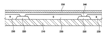
図5は、本発明の一実施形態による液晶表示装置の断面図であって、表示領域外の最外郭部の断面が示されている。第1及び第2の表示板100、200の液晶層300に接する面には配向膜190、260がそれぞれ形成されている。
FIG. 5 is a cross-sectional view of a liquid crystal display device according to an embodiment of the present invention, showing a cross section of an outermost portion outside the display area.
図5を参照する。第1の表示板100の最外郭部に設けられるデータ線162は、第2の表示板200の最外郭ブラックマトリクス225の内側に重畳して設けられる。
Please refer to FIG. The data lines 162 provided on the outermost portion of the
図5において最外郭ブラックマトリクス225によって形成される遮光領域は、非表示領域における遮光領域であって、表示領域内の遮光領域と比べて面積が格段に広い。第1の表示板100の最外郭部非表示領域の遮光領域には、画素電極182と同一層に画素電極182と分離された第1の不純物吸着電極185が表示領域内のブラックマトリクスパターン220と比べて相対的に広い幅に形成されている。第2の表示板200には、共通電極250と第2の不純物吸着電極251とが形成されている。本実施形態において第2の不純物吸着電極251は、共通電極250と一体に形成されている。すなわち、第1の不純物吸着電極185に対向する領域の電極が第2の不純物吸着電極251に相当する。
In FIG. 5, the light shielding region formed by the outermost
第1の不純物吸着電極185には、画素電圧とは別個の独立した外部電圧が印加される。第2の不純物吸着電極251には、共通電極250と同一電圧が印加される。このような第1の不純物吸着電極185と第2の不純物吸着電極251とが不純物吸着電界を生成することになる。
An independent external voltage that is separate from the pixel voltage is applied to the first
この時、第1及び第2の不純物吸着電極185、251の間に液晶層300の透過領域、すなわち画素電極182と共通電極250との間の残留DCバイアスの絶対値よりさらに大きい電位差(絶対値)が形成されるように電圧を印加すれば、隣接する画素領域内に浮遊するイオン性不純物320は画素電極182と共通電極250との間の残留DCバイアスによる電界より第1及び第2の不純物吸着電極185、251との間に形成された電位差によって、より影響を受けることになる。従って、図5に示すように、イオン性不純物320が第1及び第2の不純物吸着電極185、251に吸着する。
At this time, a potential difference (absolute value) larger than the absolute value of the residual DC bias between the transmission region of the
ここで、第2の不純物吸着電極251には、共通電圧と同一電圧が印加されるので、電位差を調節するためには第1の不純物吸着電極185に印加される外部電圧を調節する。前記電位差の絶対値は、残留DCバイアスの大きさ(絶対値)によって決定されるが、概略2V以上であれば、残留DCバイアスより大きくなる。しかしながら、これに限定されるわけではないことは言うまでもない。
Here, since the same voltage as the common voltage is applied to the second
第1の不純物吸着電極185に印加される外部電圧は、好ましくはDC電圧であればよいが、AC電圧を印加しながら第1及び第2の不純物吸着電極185、251の間に形成される電位差の絶対値が前記範囲に該当するように調節してもよい。すなわち、第1の不純物吸着電極185と第2の不純物吸着電極251との間の平均電位差の絶対値が、液晶層300の透過領域、すなわち画素領域の画素電極182と共通電極250との間に残留するDCバイアスより大きいように印加されるようにすればよく、その具体的な方法には制限はない。
The external voltage applied to the first
上述したように本実施形態による液晶表示装置においては、非表示領域である最外郭遮光領域にイオン性不純物320が吸着するので、画素領域に浮遊するイオン性不純物320の濃度が減少することになる。最外郭遮光領域は、表示領域内の遮光領域と比べて相対的に広い面積を有するので十分なイオン性不純物320吸着能力を有する。従って、画素領域内残像が発生する原因のうちの一つが除去され、残像現象を抑制することができる。
As described above, in the liquid crystal display device according to the present embodiment, since the
不純物吸着電極185、251が設けられる領域は遮光領域であるので、画像表示に直接的な影響を与えない。残像現象は、表示される画像に関係するので、遮光領域におけるイオン性不純物320の吸着は残像を誘発しない。一方、本実施形態において不純物吸着電極185、251には最外郭遮光領域に隣接したイオン性不純物320が主として吸着するが、液晶層300内においては液晶分子310が対流しているので、イオン性不純物320も液晶分子310の対流によって移動しながら最外郭遮光領域近傍に移動することになる。このように最外郭遮光領域近傍に移動したイオン性不純物320は、不純物吸着電極185、251に容易に吸着される。本実施形態では、配向膜190、260がラビングされているので、このような液晶分子310及びイオン性不純物320の対流がより活発になり、全体的に高いイオン性不純物320吸着率を得ることができる。
Since the region where the
図6は、本発明の一実施形態による液晶表示装置における第1の不純物吸着電極の配置を示す平面図である。図6においては、第1の表示板上に設けられた不純物吸着電極パターンが示されている。図6を参照すると、第1の不純物吸着電極185は、非表示領域の最外郭部に沿って形成されている。第1の不純物吸着電極185の幅は、第2の表示板の最外郭ブラックマトリクスの幅より狭いか、或いは同じである。また、第1の不純物吸着電極185は、外部電源線が接続される吸着電極パッド185aを備えるようにしてもよい。吸着電極パッド185aは、第1の不純物吸着電極185の一方側の角部に多少拡張されて形成するようにしてもよい。
FIG. 6 is a plan view showing the arrangement of the first impurity adsorption electrode in the liquid crystal display device according to the embodiment of the present invention. In FIG. 6, an impurity adsorption electrode pattern provided on the first display panel is shown. Referring to FIG. 6, the first
一方、図6に示す例とは異なり、必要に応じて第1の不純物吸着電極185が閉曲線を構成せずに一部が切れているようにしてもよい。閉曲線を構成しなくても電気的に互いに接続されていれば、一つの吸着電極パッド185aのみを備えるようにしても差し支えないが、電気的に分離された2以上の不純物吸着電極を備える場合には、それぞれに吸着電極パッド185aを備えるようにすればよい。
On the other hand, unlike the example shown in FIG. 6, the first
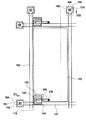
以下、前記のような本発明の一実施形態による液晶表示装置の駆動について説明する。図7は、本発明の一実施形態による液晶表示装置のブロック図である。 Hereinafter, driving of the liquid crystal display device according to the embodiment of the present invention will be described. FIG. 7 is a block diagram of a liquid crystal display device according to an embodiment of the present invention.
図7を参照する。液晶表示装置は、液晶パネル400を駆動する駆動部としてゲート駆動部410及びデータ駆動部420を有しており、これらを制御する信号制御部430、これらの駆動に必要な電圧を生成する駆動電圧生成部440及び階調電圧を生成する階調電圧生成部450を含んでいる。
Please refer to FIG. The liquid crystal display device includes a
信号制御部430は、ゲート駆動部410及びデータ駆動部420と接続されており、これらの動作を制御する制御信号を生成し供給する。信号制御部430は、外部のグラフィック制御器(図示せず)から映像信号(R、G、B)及び映像信号の表示を制御する入力制御信号を受信する。なお、受信した入力制御信号としては、例えば、垂直同期信号(Vsync)、水平同期信号(Hsync)、メインクロック(MCLK)、データイネーブル信号(DE)などがある。
The
信号制御部430は、上述したような入力制御信号に基づいてゲート制御信号(CONT1)及びデータ制御信号(CONT2)などを生成し、映像信号(R、G、B)を液晶パネルの動作条件に合うように処理した後、ゲート制御信号(CONT1)をゲート駆動部410に送り、データ制御信号(CONT2)及び処理されたデータ信号(R´、G´、B´)をデータ駆動部420に送る。
The
データ駆動部420には、信号制御部410からのデータ制御信号(CONT2)に応じて一つの行の画素に対応する映像データ(R´、G´、B´)が順に入力される。データ駆動部420は、階調電圧生成部450からの階調電圧のうち各映像データ(R´、G´、B´)に対応する階調電圧を選択することによって、映像データ(R´、G´、B´)を当該データ電圧に変換する。
Video data (R ′, G ′, B ′) corresponding to pixels in one row is sequentially input to the
ゲート駆動部410は、信号制御部430からゲート制御信号(CONT1)に応じてゲートオン電圧(Von)をゲート線(G1〜Gn)に印加することによって、そのゲート線(G1〜Gn)に接続された薄膜トランジスタをターンオンする。
The
駆動電圧生成部440は、ゲートオン電圧(Von)及びゲートオフ電圧(Voff)を生成してゲート駆動部410に供給する。また、駆動電圧生成部440は、第1の不純物吸着電圧(Va1)を生成して液晶パネル400の第1の表示板の第1の不純物吸着電極に印加し、共通電圧(Vcom)を生成して第2の表示板の共通電極及びそれと一体に形成されている第2の不純物吸着電極に印加する。このように印加された第1の不純物吸着電圧(Va1)及び共通電圧(Vcom)は、不純物吸着電界を生成するようになる。本実施形態で第2の不純物吸着電極は、共通電極と接続されているので、別途第2の不純物吸着電圧が印加されるわけではなく、共通電圧(Vcom)がそのまま印加されるようになる。
The driving
図8は、本発明の他の実施形態による液晶表示装置の断面図であって、表示領域内の断面が示されている。図8の実施形態による液晶表示装置は図5に示されている液晶表示装置と実質的に同一な構造を有するが、第1及び第2の表示板100、200の最外郭部ではない表示領域の内側の遮光領域にそれぞれ第1及び第2の不純物吸着電極186、251を備えている点で異なる。以下の説明においては、重複する部分について容易に理解又は類推できる範囲内でその説明を省略し、差異点を中心に説明する。
FIG. 8 is a cross-sectional view of a liquid crystal display device according to another embodiment of the present invention, and shows a cross section in the display region. The liquid crystal display device according to the embodiment of FIG. 8 has substantially the same structure as the liquid crystal display device shown in FIG. 5, but is not the outermost portion of the first and
図8を参照する。第1の表示板100のデータ線162は、第2の表示板200のブラックマトリクスパターン220の内側に重畳して設けられる。また、図8では示さないが、第1の表示板100のゲート線は、第2の表示板200のブラックマトリクスパターン220の内側に重畳して設けられている。このようなデータ線162、ゲート線及びブラックマトリクスパターン220は実質的に遮光領域を形成する。
Please refer to FIG. The data lines 162 of the
第1の表示板100の保護膜170上には、データ線162と重畳するように第1の不純物吸着電極186が形成されている。図示しないが、第1の不純物吸着電極186は、ゲート線と重畳して形成されるようにしてもよく、ゲート線とデータ線162とのうちいずれか一つにのみ重畳されるように形成されるようにしてもよく、また、これら全てに重畳されるように形成されるようにしてもよい。すなわち、第1の不純物吸着電極186は、ゲート線、データ線162及びブラックマトリクスパターン220によって定義される遮光領域内に形成される。
A first
第1の不純物吸着電極186は、画素電極182と同一層に設けられるが、画素電極182と分離されている。第1の不純物吸着電極186は画素電極182と同一物質、例えば、ITO、IZOなどの透明な導電性物質からなるようにすればよい。また、第1の不純物吸着電極186は、画素電極182と同時にパターニングすることによって形成することができる。
The first
第2の表示板200には、第2の不純物吸着電極251及び共通電極250が形成されている。本実施形態で第2の不純物吸着電極251は、共通電極250と一体に形成されており、第1の不純物吸着電極186に対向する遮光領域に設けられる電極が第2の不純物吸着電極251に相当することになる。
A second
このように本実施形態では、表示領域内側の遮光領域に設けられる第1及び第2の不純物吸着電極186、251によって不純物吸着電界が形成される。本実施形態においても、図5の実施形態と同様、画素電極182と共通電極250との間の残留DCバイアスの絶対値より第1及び第2の不純物吸着電極186、251の間の電位差の絶対値がさらに大きいように第1及び第2の不純物吸着電極186、251に電圧が印加される。例えば、2V以上の電位差を有するように印加するようにすればよい。従って、透過領域である画素領域に浮遊するイオン性不純物320が、遮光領域に設けられる第1及び第2の不純物吸着電極186、251の間に形成された電位差に影響を受け、第1及び第2の不純物吸着電極186、251に吸着される。従って、画素領域内のイオン性不純物320の濃度が減少するようになり、残像現象が抑制される。
Thus, in this embodiment, an impurity adsorption electric field is formed by the first and second
図9は、本発明の他の実施形態による液晶表示装置における第1の不純物吸着電極の配置を示す平面図である。図9においては、第1の表示板上に設けられる第1の不純物吸着電極パターンが示されている。図9を参照すれば、第1の不純物吸着電極186は、表示領域内部の遮光領域に沿って格子状に形成されており、全て一体に接続されている。第1の不純物吸着電極186は外部電源線が接続される吸着電極パッド186aを備えるようにしてもよい。吸着電極パッド186aは、第1の不純物吸着電極パターン186のいずれか一つの端部が延長され拡張された形状を有するようにしてもよい。吸着電極パッド186aは、第1の表示板の補助ゲートパッド又は補助データパッドのいずれか一つに隣接して設けられるようにしてもよい。
FIG. 9 is a plan view showing the arrangement of the first impurity adsorption electrode in the liquid crystal display device according to another embodiment of the present invention. FIG. 9 shows a first impurity adsorption electrode pattern provided on the first display panel. Referring to FIG. 9, the first
一方、第1の不純物吸着電極パターン186は、表示領域内の全ての遮光領域に設けられなければならないわけではなく、必要に応じて、行又は列のうちいずれか一つにのみ形成されるようにしてもよく、一部の領域が省略され形成されるようにしてもよい。さらに多様な変形例が可能なことは言うまでもない。
On the other hand, the first impurity
以上説明した図6の実施形態と図9の実施形態とは、互いに排他的ではなく、相互に組み合わせることが可能である。このような組み合わせの例が図10に示されている。 The embodiment of FIG. 6 and the embodiment of FIG. 9 described above are not mutually exclusive and can be combined with each other. An example of such a combination is shown in FIG.
図10は、本発明のさらに他の実施形態による液晶表示装置における第1の不純物吸着電極の配置を示す平面図である。図10を参照すれば、第1の不純物吸着電極185、186が非表示領域の最外郭遮光領域だけではなく、表示領域内の遮光領域にも配置されている。従って、最外郭遮光領域に隣接したイオン性不純物が、広い面積を有する最外郭部の不純物吸着電極185に十分に吸着される。また、最外郭遮光領域から離れている画素領域のイオン性不純物も周辺に設けられる表示領域内の不純物吸着電極186に容易に吸着され、液晶層の透過領域、すなわち画素領域の画素電極と共通電極との間に浮遊するイオン性不純物の濃度がさらに減少するようになる。従って、残像現象をより抑制することがきる。
FIG. 10 is a plan view showing the arrangement of the first impurity adsorption electrode in the liquid crystal display device according to still another embodiment of the present invention. Referring to FIG. 10, the first
以上の実施形態においては液晶表示装置としてTNモード方式が採用された例を挙げているが、本発明はそれに限定されるわけではない。以下の説明においては、本発明が他の方式の液晶表示装置に適用された例を説明する。図11は、本発明のさらに他の実施形態による液晶表示装置の断面図である。 In the above embodiment, an example in which the TN mode method is adopted as the liquid crystal display device is described, but the present invention is not limited thereto. In the following description, an example in which the present invention is applied to another type of liquid crystal display device will be described. FIG. 11 is a cross-sectional view of a liquid crystal display device according to another embodiment of the present invention.
図11の液晶表示装置は、以上の実施形態とは異なり、液晶層301の液晶分子311が垂直に配向している。液晶層300に含まれる液晶分子は、例えば、負の誘電率異方性を有するようにすればよい。また、一つの画素において第1の表示板101の画素電極182がパターニングされており、且つ、第2の表示板201の共通電極250もパターニングされている。画素電極182及び共通電極250パターンは、一つの画素を複数のドメインに分けることになる。各ドメインにおいては、それぞれ液晶分子301が動く方向を異にする。
In the liquid crystal display device of FIG. 11, unlike the above embodiment, the
第1の表示板101の最外郭部非表示領域の遮光領域には画素電極182と同一層に画素電極182と分離された第1の不純物吸着電極185が表示領域内のブラックマトリクスパターン240などと比べて相対的に広い幅で形成されている。第2の表示板201には、共通電極250と第2の不純物吸着電極252とが形成されている。なお、第2の不純物吸着電極252は共通電極250と電気的に分離されており、最外郭部ブラックマトリクス225下で第1の不純物吸着電極185と対向するように設けられる。第2の不純物吸着電極252は、共通電極250と同一物質、例えば、ITO、IZOなどの透明な導電性物質からなるよういにすればよく、ドメイン形成のための共通電極250のパターニング工程時に同時にパターニングすることによって形成することができる。
The first
第2の不純物吸着電極252は、共通電極250とは独立した外部電圧である第2の不純物吸着電圧が印加され、第1の不純物吸着電極185に印加される第1の不純物吸着電圧と共に電位差を生じさせ、不純物吸着電界を生成するようになる。本実施形態では、第1の不純物吸着電極だけではなく、第2の不純物吸着電極に対しても独立した電圧を印加することができるので、より容易に不純物吸着電界の調節が可能となる。一つの電極に共通電圧が固定されて印加される場合と比べて、印加電圧の大きさを小さくすることができる。しかしながら、この場合においても、図5の実施形態において説明したように、第1の不純物吸着電極185と第2の不純物吸着電極252との間の平均電位差の絶対値が液晶層301の透過領域、すなわち画素領域の画素電極182と共通電極250との間に残留するDCバイアスより大きいように印加されなければならないことは説明したとおりである。
The second
このような第2の不純物吸着電圧は、液晶表示装置の駆動電圧生成部で第1の不純物吸着電圧と共に生成することができる。しかしながら、それに限定されるわけではなく、追加的に第2の不純物吸着電圧生成部を備えてもよい。 Such a second impurity adsorption voltage can be generated together with the first impurity adsorption voltage in the drive voltage generation unit of the liquid crystal display device. However, the present invention is not limited to this, and a second impurity adsorption voltage generation unit may be additionally provided.
図12は、本発明のさらに他の実施形態による液晶表示装置の断面図である。 FIG. 12 is a cross-sectional view of a liquid crystal display device according to another embodiment of the present invention.
本実施形態による液晶表示装置は、第1及び第2の表示板の最外郭部ではない第1及び第2の不純物吸着電極186、252が表示領域の内側の遮光領域に備えられる点を除いては、図11の実施形態による液晶表示装置と同様である。ここで、第1の不純物吸着電極186は、第1の表示板101のゲート線及び/又はデータ線162上に形成される。なお、第1の不純物吸着電極186は、画素電極182とは分離されている。また、第2の不純物吸着電極252は、第2の表示板202の共通電極250と分離されて形成されている。その他具体的な差異点は、本技術分野の当業者であれば本明細書を通して容易に理解、類推できるため、ここではその説明は省略する。
In the liquid crystal display device according to the present embodiment, the first and second
また、図11の実施形態と図12の実施形態を組み合わせて、非表示領域の遮光領域と表示領域の遮光領域とに第1及び第2の不純物吸着電極を全て形成してもよい。 11 and 12 may be combined to form all the first and second impurity adsorption electrodes in the light shielding area of the non-display area and the light shielding area of the display area.
一方、以上の実施形態では、共通電極がパターニングされている場合、共通電極と第2の不純物吸着電極とが分離された構造を有し、第2の不純物吸着電極に共通電圧とは別の電圧が印加される場合が例示されているが、これに限定されるわけではなく、共通電極がパターニングされていない場合であっても、共通電極と分離された第2の不純物吸着電極を備えるようにしてもよい。 On the other hand, in the above embodiment, when the common electrode is patterned, the common electrode and the second impurity adsorption electrode are separated from each other, and the second impurity adsorption electrode has a voltage different from the common voltage. However, the present invention is not limited to this, and the second impurity adsorption electrode separated from the common electrode is provided even when the common electrode is not patterned. May be.
また、共通電極が第1の表示板に備えられている場合、例えば、IPS(In−Plane Switching)モード液晶表示装置、PLS(Plane to Line Switching)モード液晶表示装置などにおいても第2の表示板に独立した第2の不純物吸着電極を形成することによって、本発明の技術的思想を同様一に適用することができる。このような場合も本発明の技術的範囲に属することと看做さなければならない。 In the case where the first display panel is provided with the common electrode, for example, the second display panel also in an IPS (In-Plane Switching) mode liquid crystal display device, a PLS (Plane to Line Switching) mode liquid crystal display device, or the like. By forming the second impurity adsorption electrode independent of each other, the technical idea of the present invention can be similarly applied. Such a case must also be regarded as belonging to the technical scope of the present invention.
以上、本発明の実施形態による表示装置として液晶を含む媒体を備える液晶表示装置について例示したが、上述したように本発明による表示装置及びその駆動方法がそれに限定されるわけではなく、他の表示装置及び駆動方法にも適用可能である。例えば、媒体として流体及び荷電粒子を含む電気泳動表示装置及びその駆動方法にも同様に適用することができる。この場合、本明細書において、液晶表示装置において定義された透過領域には荷電粒子を備えて、外部の光を反射することによって表示領域を構成する空間部が対応することになる。同様に、遮光領域には、隔壁又はその他支持パターンのように画像の表示と関係ない領域が対応することになる。このような本発明の実施形態による電気泳動表示装置においても、遮光領域に不純物吸着電極を備えることによって、遮光領域に存在するイオン性不純物を除去し残像現象を減少させることができる。なお、好ましくは、不純物吸着電極と空間部とが空間的に接続された構造を有するようにしてもよい。その外の本実施形態による電気泳動表示装置の構造については、本発明の属する技術分野の当業者によく知られているか、或いは容易に類推できることであるため、ここでは具体的な説明は省略する。 As described above, the liquid crystal display device including the medium including the liquid crystal is illustrated as the display device according to the embodiment of the present invention. However, as described above, the display device according to the present invention and the driving method thereof are not limited thereto, and other displays are possible. The present invention can also be applied to an apparatus and a driving method. For example, the present invention can be similarly applied to an electrophoretic display device including a fluid and charged particles as a medium and a driving method thereof. In this case, in this specification, the transmissive region defined in the liquid crystal display device includes charged particles and corresponds to a space portion that forms the display region by reflecting external light. Similarly, the light shielding area corresponds to an area not related to image display, such as a partition wall or other support pattern. Also in the electrophoretic display device according to the embodiment of the present invention, by providing the impurity adsorption electrode in the light shielding region, the ionic impurities existing in the light shielding region can be removed and the afterimage phenomenon can be reduced. In addition, Preferably, you may make it have a structure where the impurity adsorption electrode and the space part were spatially connected. The remaining structure of the electrophoretic display device according to the present embodiment is well known to those skilled in the art to which the present invention pertains or can be easily analogized. .
以上、添付した図面を参照して本発明の好ましい実施形態について説明したが、当業者であれば、本発明の技術的思想や必須な特徴を変更せずに、本発明が他の具体的な形態で実施され得ることを理解することができる。したがって、上述した好ましい実施形態は、例示的なものであり、限定的なものではないと理解されるべきである。 The preferred embodiments of the present invention have been described above with reference to the accompanying drawings. However, those skilled in the art will recognize that the present invention is not limited to other specific embodiments without changing the technical idea and essential features of the present invention. It can be understood that it can be implemented in the form. Accordingly, the preferred embodiments described above are to be understood as illustrative and not restrictive.
本発明は、液晶表示装置、電気泳動表示装置などのような表示装置に適用され得る。 The present invention can be applied to display devices such as liquid crystal display devices and electrophoretic display devices.
100:第1の表示板
182:画素電極
185、186:第1の不純物吸着電極
200:第2の表示板
250:共通電極
251、252:第2の不純物吸着電極
300:液晶層
320:イオン性不純物
400:液晶パネル
100: first display panel 182:
Claims (9)
前記第1の不純物吸着電極と対向する前記遮光領域に形成された第2の不純物吸着電極を含み、前記第1の表示板に対向する第2の表示板と、
前記第1及び第2の表示板との間に介在する媒体とを含むことを特徴とする表示装置。 A plurality of gate lines extending in parallel to the first direction; a plurality of data lines extending in parallel to the second direction ; a pixel electrode formed in a transmissive region; A first display panel that includes a first impurity adsorption electrode that is separated from an electrode and is formed to be insulated and overlapped with the gate line and the data line ;
A second display panel that includes the second impurity adsorption electrode formed in the light shielding region facing the first impurity adsorption electrode, and that opposes the first display panel;
And a medium interposed between the first and second display panels.
前記第1の不純物吸着電極と対向する第2の不純物吸着電極を含み、前記第1の表示板に対向する第2の表示板と、
前記第1及び第2の表示板との間に介在する媒体を含み、
前記第1の不純物吸着電極は、画素毎に形成されたそれぞれの薄膜トランジスタの制御端子に接続されたゲート線及び前記薄膜トランジスタの入力端子に接続されたデータ線と絶縁されて重畳するように表示領域内側に延長された吸着電極領域をさらに含み、
前記第2の不純物吸着電極は、前記第1の不純物吸着電極に対向するように表示領域の内側に延長された吸着電極領域をさらに含むことを特徴とする表示装置。 A first display panel including a first impurity adsorption electrode formed on the outermost periphery of the display region and separated from the pixel electrode;
A second display panel that includes a second impurity adsorption electrode facing the first impurity adsorption electrode, and that opposes the first display panel;
Look containing a medium interposed between the first and second display panels,
The first impurity adsorbing electrode is arranged on the inner side of the display region so as to be insulated and overlapped with a gate line connected to a control terminal of each thin film transistor formed for each pixel and a data line connected to the input terminal of the thin film transistor. Further comprising an adsorption electrode region extended to
Said second impurity adsorption electrode, the display characterized by further including Mukoto adsorption electrode region which extends inside the display region so as to face the first impurity adsorption electrode device.
前記薄膜トランジスタの入力端子に接続されたデータ線、
前記薄膜トランジスタの出力端子に接続された画素電極、及び、
前記ゲート線及び前記データ線と絶縁されて重畳して形成され、前記画素電極と分離された第1の不純物吸着電極を備える第1の表示板と、
格子状のブラックマトリクスパターン、及び、
前記ブラックマトリクスパターン下に重畳されて形成され、前記第1の不純物吸着電極と対向する第2の不純物吸着電極を含み、前記第1の表示板に対向する第2の表示板と、
前記第1及び第2の表示板との間に介在する液晶層とを含むことを特徴とする表示装置。 A gate line connected to a control terminal of each thin film transistor formed for each pixel;
A data line connected to an input terminal of the thin film transistor;
A pixel electrode connected to the output terminal of the thin film transistor; and
Is formed by overlapping are insulated from the gate line及beauty before Symbol data lines, a first panel comprising a first impurity adsorption electrode which is separated from the pixel electrode,
Grid-like black matrix pattern, and
A second display panel that is formed to be superimposed under the black matrix pattern and includes a second impurity adsorption electrode facing the first impurity adsorption electrode, and facing the first display panel;
And a liquid crystal layer interposed between the first and second display panels.
前記第1及び第2の不純物吸着電極間平均電位差が2V以上であることを特徴とする請求項5に記載の表示装置。 In the first impurity adsorption electrode and the second impurity adsorption electrode, the absolute value of the average potential difference between the first and second impurity adsorption electrodes is smaller than the absolute value of the DC bias remaining in the transmission region of the medium. The voltage is applied so that it is large,
The display device according to claim 5, wherein an average potential difference between the first and second impurity adsorption electrodes is 2 V or more.
前記第1の不純物吸着電極に第1の電圧を印加する段階と、
前記第2の不純物吸着電極に第2の電圧を印加する段階と、
前記第1の不純物吸着電極と前記第2の不純物吸着電極とに前記第1及び第2の不純物吸着電極間平均電位差の絶対値が前記媒体の透過領域に残留するDCバイアスの絶対値より大きいように電圧を印加することを含むことを特徴とする表示装置の駆動方法。 A plurality of gate lines extending in parallel to the first direction; a plurality of data lines extending in parallel to the second direction ; a pixel electrode formed in a transmissive region; A first display panel including a first impurity adsorption electrode which is separated from an electrode and is formed so as to be insulated and overlapped with the gate line and the data line; and the light shielding which faces the first impurity adsorption electrode A display including a second impurity adsorption electrode formed in the region and facing the first display panel, and a medium interposed between the first and second display panels A method for driving an apparatus, comprising:
Applying a first voltage to the first impurity adsorption electrode;
Applying a second voltage to the second impurity adsorption electrode;
The absolute value of the average potential difference between the first and second impurity adsorption electrodes is larger than the absolute value of the DC bias remaining in the transmission region of the medium between the first impurity adsorption electrode and the second impurity adsorption electrode. A method for driving a display device, comprising applying a voltage to the display device.
Applications Claiming Priority (2)
| Application Number | Priority Date | Filing Date | Title |
|---|---|---|---|
| KR10-2005-0118173 | 2005-12-06 | ||
| KR1020050118173A KR20070059385A (en) | 2005-12-06 | 2005-12-06 | Display apparatus |
Publications (3)
| Publication Number | Publication Date |
|---|---|
| JP2007156416A JP2007156416A (en) | 2007-06-21 |
| JP2007156416A5 JP2007156416A5 (en) | 2009-05-28 |
| JP4980002B2 true JP4980002B2 (en) | 2012-07-18 |
Family
ID=38139938
Family Applications (1)
| Application Number | Title | Priority Date | Filing Date |
|---|---|---|---|
| JP2006200604A Active JP4980002B2 (en) | 2005-12-06 | 2006-07-24 | Display device |
Country Status (3)
| Country | Link |
|---|---|
| US (1) | US7791680B2 (en) |
| JP (1) | JP4980002B2 (en) |
| KR (1) | KR20070059385A (en) |
Families Citing this family (21)
| Publication number | Priority date | Publication date | Assignee | Title |
|---|---|---|---|---|
| JP2008020725A (en) * | 2006-07-13 | 2008-01-31 | Sony Corp | Liquid crystal display and video display |
| US8674971B2 (en) * | 2007-05-08 | 2014-03-18 | Japan Display West Inc. | Display device and electronic apparatus including display device |
| TWI363240B (en) * | 2008-03-31 | 2012-05-01 | Au Optronics Corp | Active array substrate, electrode substrate, and liquid crystal display panel |
| CN102023447B (en) * | 2008-04-08 | 2014-04-16 | 友达光电股份有限公司 | Electrode substrate and liquid crystal display panel |
| US8144277B2 (en) * | 2008-05-02 | 2012-03-27 | Canon Kabushiki Kaisha | Liquid crystal display device |
| JP2010026032A (en) * | 2008-07-16 | 2010-02-04 | Mitsubishi Electric Corp | Liquid crystal display device |
| KR101889287B1 (en) | 2008-09-19 | 2018-08-20 | 가부시키가이샤 한도오따이 에네루기 켄큐쇼 | Semiconductor device |
| JP2012083513A (en) * | 2010-10-12 | 2012-04-26 | Seiko Epson Corp | Liquid crystal device, and electronic device |
| CN102540526A (en) * | 2010-12-31 | 2012-07-04 | 奇美电子股份有限公司 | Vertical alignment LCD (liquid crystal display) and driving method thereof |
| JP5790256B2 (en) | 2011-07-29 | 2015-10-07 | セイコーエプソン株式会社 | Electro-optical device, driving method of electro-optical device, electronic apparatus, projector |
| KR20140039570A (en) * | 2012-09-24 | 2014-04-02 | 한국전자통신연구원 | Color electronic paper display and forming the same |
| KR20140053626A (en) * | 2012-10-26 | 2014-05-08 | 삼성디스플레이 주식회사 | Display apparatus and organic luminescense display apparatus |
| KR20140053653A (en) | 2012-10-26 | 2014-05-08 | 삼성디스플레이 주식회사 | Liquid crystal display and method for fabricating the same |
| CN102998856B (en) * | 2012-11-19 | 2015-03-25 | 京东方科技集团股份有限公司 | Array substrate, as well as manufacture method and display device thereof |
| CN103941484A (en) * | 2014-04-30 | 2014-07-23 | 京东方科技集团股份有限公司 | Flexible liquid crystal display panel and manufacturing method thereof |
| JP2016057427A (en) * | 2014-09-09 | 2016-04-21 | セイコーエプソン株式会社 | Electro-optic device and electronic equipment |
| CN105044971B (en) * | 2015-08-27 | 2018-11-23 | 昆山龙腾光电有限公司 | Liquid crystal display device |
| KR102607402B1 (en) * | 2016-10-31 | 2023-11-30 | 엘지디스플레이 주식회사 | Gate driving circuit and display device using the same |
| JP6844306B2 (en) * | 2017-02-24 | 2021-03-17 | セイコーエプソン株式会社 | Electro-optic device and how to drive the electro-optic device |
| CN109216926B (en) * | 2017-07-06 | 2022-03-11 | 群创光电股份有限公司 | Radiation device |
| CN110767191A (en) * | 2019-10-24 | 2020-02-07 | 深圳市华星光电半导体显示技术有限公司 | Pixel driving circuit structure of liquid crystal display panel |
Family Cites Families (12)
| Publication number | Priority date | Publication date | Assignee | Title |
|---|---|---|---|---|
| JPH08201830A (en) * | 1995-01-27 | 1996-08-09 | Citizen Watch Co Ltd | Liquid crystal display device |
| JPH10253953A (en) * | 1997-03-10 | 1998-09-25 | Hitachi Ltd | Liquid crystal display device |
| JP2000284319A (en) * | 1999-03-30 | 2000-10-13 | Matsushita Electric Ind Co Ltd | Production of active matrix liquid crystal display device and its display device |
| JP3497098B2 (en) * | 1999-05-25 | 2004-02-16 | シャープ株式会社 | Liquid crystal display device |
| JP2002006300A (en) | 2000-06-19 | 2002-01-09 | Matsushita Electric Ind Co Ltd | Liquid crystal element, its manufacturing method and its drive method |
| JP2001166322A (en) | 1999-12-07 | 2001-06-22 | Seiko Epson Corp | Liquid crystal device and electronic equipment |
| JP2001201734A (en) | 2000-01-21 | 2001-07-27 | Sharp Corp | Liquid crystal display device |
| JP3384398B2 (en) * | 2000-05-25 | 2003-03-10 | セイコーエプソン株式会社 | Liquid crystal device, manufacturing method thereof, and electronic equipment |
| JP2002014365A (en) * | 2000-06-30 | 2002-01-18 | Casio Comput Co Ltd | Liquid crystal display element |
| JP2002196355A (en) * | 2000-12-27 | 2002-07-12 | Casio Comput Co Ltd | Liquid crystal display device |
| JP4614726B2 (en) * | 2003-11-25 | 2011-01-19 | シャープ株式会社 | Liquid crystal display device |
| JP2005275144A (en) * | 2004-03-25 | 2005-10-06 | Sharp Corp | Liquid crystal display device |
-
2005
- 2005-12-06 KR KR1020050118173A patent/KR20070059385A/en not_active Application Discontinuation
-
2006
- 2006-07-24 JP JP2006200604A patent/JP4980002B2/en active Active
- 2006-12-06 US US11/567,378 patent/US7791680B2/en active Active
Also Published As
| Publication number | Publication date |
|---|---|
| US20070134883A1 (en) | 2007-06-14 |
| US7791680B2 (en) | 2010-09-07 |
| KR20070059385A (en) | 2007-06-12 |
| JP2007156416A (en) | 2007-06-21 |
Similar Documents
| Publication | Publication Date | Title |
|---|---|---|
| JP4980002B2 (en) | Display device | |
| KR101171414B1 (en) | Liquid crystal display device | |
| US9640122B2 (en) | Liquid crystal display device and driving method thereof | |
| JP7390895B2 (en) | Array substrates, display panels and display devices | |
| JP4667587B2 (en) | Liquid crystal display device | |
| JP6804256B2 (en) | Liquid crystal display panel and liquid crystal display device | |
| KR101522241B1 (en) | Liquid crystal display device controllable viewing angle and method of fabricating the same | |
| JP2007226175A (en) | Liquid crystal device and electronic equipment | |
| KR20080001957A (en) | Display substrate and display panel having the same | |
| WO2010131552A1 (en) | Liquid crystal display device | |
| JP2014115434A (en) | Array substrate and display device | |
| JP2007226200A (en) | Liquid crystal device, and electronic device | |
| US10890815B2 (en) | Display apparatus | |
| KR20060114742A (en) | Liquid crystal display panel and manufacturing method of the same | |
| KR101331905B1 (en) | Thin film transistor and method of fabricating the same | |
| KR20070072275A (en) | Vertical alignment mode liquid crystal display device and method of fabricating thereof | |
| KR20070002779A (en) | Liquid crystal display and method for fabricating the same | |
| JP4593161B2 (en) | Liquid crystal display | |
| KR102098161B1 (en) | Array substrate for liquid crystal display | |
| KR101971143B1 (en) | Liquid Crystal Display Device And Method Of Fabricating The Same | |
| JP5534655B2 (en) | ELECTRO-OPTICAL DEVICE, MANUFACTURING METHOD THEREOF, AND ELECTRONIC DEVICE | |
| JP4121357B2 (en) | Liquid crystal display | |
| US11003031B2 (en) | Display apparatus | |
| JP2007226199A (en) | Liquid crystal device, and electronic equipment | |
| JPH1048672A (en) | Active matrix type liquid crystal display device |
Legal Events
| Date | Code | Title | Description |
|---|---|---|---|
| A521 | Request for written amendment filed |
Free format text: JAPANESE INTERMEDIATE CODE: A523 Effective date: 20090415 |
|
| A621 | Written request for application examination |
Free format text: JAPANESE INTERMEDIATE CODE: A621 Effective date: 20090415 |
|
| A977 | Report on retrieval |
Free format text: JAPANESE INTERMEDIATE CODE: A971007 Effective date: 20111226 |
|
| A131 | Notification of reasons for refusal |
Free format text: JAPANESE INTERMEDIATE CODE: A131 Effective date: 20120117 |
|
| A521 | Request for written amendment filed |
Free format text: JAPANESE INTERMEDIATE CODE: A523 Effective date: 20120307 |
|
| TRDD | Decision of grant or rejection written | ||
| A01 | Written decision to grant a patent or to grant a registration (utility model) |
Free format text: JAPANESE INTERMEDIATE CODE: A01 Effective date: 20120410 |
|
| A01 | Written decision to grant a patent or to grant a registration (utility model) |
Free format text: JAPANESE INTERMEDIATE CODE: A01 |
|
| A61 | First payment of annual fees (during grant procedure) |
Free format text: JAPANESE INTERMEDIATE CODE: A61 Effective date: 20120418 |
|
| FPAY | Renewal fee payment (event date is renewal date of database) |
Free format text: PAYMENT UNTIL: 20150427 Year of fee payment: 3 |
|
| R150 | Certificate of patent or registration of utility model |
Ref document number: 4980002 Country of ref document: JP Free format text: JAPANESE INTERMEDIATE CODE: R150 Free format text: JAPANESE INTERMEDIATE CODE: R150 |
|
| FPAY | Renewal fee payment (event date is renewal date of database) |
Free format text: PAYMENT UNTIL: 20150427 Year of fee payment: 3 |
|
| S111 | Request for change of ownership or part of ownership |
Free format text: JAPANESE INTERMEDIATE CODE: R313111 |
|
| FPAY | Renewal fee payment (event date is renewal date of database) |
Free format text: PAYMENT UNTIL: 20150427 Year of fee payment: 3 |
|
| R371 | Transfer withdrawn |
Free format text: JAPANESE INTERMEDIATE CODE: R371 |
|
| S111 | Request for change of ownership or part of ownership |
Free format text: JAPANESE INTERMEDIATE CODE: R313111 |
|
| R350 | Written notification of registration of transfer |
Free format text: JAPANESE INTERMEDIATE CODE: R350 |
|
| R250 | Receipt of annual fees |
Free format text: JAPANESE INTERMEDIATE CODE: R250 |
|
| R250 | Receipt of annual fees |
Free format text: JAPANESE INTERMEDIATE CODE: R250 |
|
| R250 | Receipt of annual fees |
Free format text: JAPANESE INTERMEDIATE CODE: R250 |
|
| R250 | Receipt of annual fees |
Free format text: JAPANESE INTERMEDIATE CODE: R250 |
|
| R250 | Receipt of annual fees |
Free format text: JAPANESE INTERMEDIATE CODE: R250 |
|
| R250 | Receipt of annual fees |
Free format text: JAPANESE INTERMEDIATE CODE: R250 |
|
| R250 | Receipt of annual fees |
Free format text: JAPANESE INTERMEDIATE CODE: R250 |
|
| R250 | Receipt of annual fees |
Free format text: JAPANESE INTERMEDIATE CODE: R250 |
|
| S531 | Written request for registration of change of domicile |
Free format text: JAPANESE INTERMEDIATE CODE: R313531 |
|
| R350 | Written notification of registration of transfer |
Free format text: JAPANESE INTERMEDIATE CODE: R350 |
|
| RD02 | Notification of acceptance of power of attorney |
Free format text: JAPANESE INTERMEDIATE CODE: R3D02 |
|
| R250 | Receipt of annual fees |
Free format text: JAPANESE INTERMEDIATE CODE: R250 |
|
| R250 | Receipt of annual fees |
Free format text: JAPANESE INTERMEDIATE CODE: R250 |