JP4977207B2 - LIGHTING DEVICE AND DISPLAY DEVICE USING THE SAME - Google Patents
LIGHTING DEVICE AND DISPLAY DEVICE USING THE SAME Download PDFInfo
- Publication number
- JP4977207B2 JP4977207B2 JP2009525295A JP2009525295A JP4977207B2 JP 4977207 B2 JP4977207 B2 JP 4977207B2 JP 2009525295 A JP2009525295 A JP 2009525295A JP 2009525295 A JP2009525295 A JP 2009525295A JP 4977207 B2 JP4977207 B2 JP 4977207B2
- Authority
- JP
- Japan
- Prior art keywords
- light emitting
- light
- light source
- led
- chassis
- Prior art date
- Legal status (The legal status is an assumption and is not a legal conclusion. Google has not performed a legal analysis and makes no representation as to the accuracy of the status listed.)
- Expired - Fee Related
Links
Images


Classifications
-
- G—PHYSICS
- G02—OPTICS
- G02F—OPTICAL DEVICES OR ARRANGEMENTS FOR THE CONTROL OF LIGHT BY MODIFICATION OF THE OPTICAL PROPERTIES OF THE MEDIA OF THE ELEMENTS INVOLVED THEREIN; NON-LINEAR OPTICS; FREQUENCY-CHANGING OF LIGHT; OPTICAL LOGIC ELEMENTS; OPTICAL ANALOGUE/DIGITAL CONVERTERS
- G02F1/00—Devices or arrangements for the control of the intensity, colour, phase, polarisation or direction of light arriving from an independent light source, e.g. switching, gating or modulating; Non-linear optics
- G02F1/01—Devices or arrangements for the control of the intensity, colour, phase, polarisation or direction of light arriving from an independent light source, e.g. switching, gating or modulating; Non-linear optics for the control of the intensity, phase, polarisation or colour
- G02F1/13—Devices or arrangements for the control of the intensity, colour, phase, polarisation or direction of light arriving from an independent light source, e.g. switching, gating or modulating; Non-linear optics for the control of the intensity, phase, polarisation or colour based on liquid crystals, e.g. single liquid crystal display cells
- G02F1/133—Constructional arrangements; Operation of liquid crystal cells; Circuit arrangements
- G02F1/1333—Constructional arrangements; Manufacturing methods
- G02F1/1335—Structural association of cells with optical devices, e.g. polarisers or reflectors
- G02F1/1336—Illuminating devices
- G02F1/133602—Direct backlight
- G02F1/133603—Direct backlight with LEDs
-
- G—PHYSICS
- G02—OPTICS
- G02F—OPTICAL DEVICES OR ARRANGEMENTS FOR THE CONTROL OF LIGHT BY MODIFICATION OF THE OPTICAL PROPERTIES OF THE MEDIA OF THE ELEMENTS INVOLVED THEREIN; NON-LINEAR OPTICS; FREQUENCY-CHANGING OF LIGHT; OPTICAL LOGIC ELEMENTS; OPTICAL ANALOGUE/DIGITAL CONVERTERS
- G02F1/00—Devices or arrangements for the control of the intensity, colour, phase, polarisation or direction of light arriving from an independent light source, e.g. switching, gating or modulating; Non-linear optics
- G02F1/01—Devices or arrangements for the control of the intensity, colour, phase, polarisation or direction of light arriving from an independent light source, e.g. switching, gating or modulating; Non-linear optics for the control of the intensity, phase, polarisation or colour
- G02F1/13—Devices or arrangements for the control of the intensity, colour, phase, polarisation or direction of light arriving from an independent light source, e.g. switching, gating or modulating; Non-linear optics for the control of the intensity, phase, polarisation or colour based on liquid crystals, e.g. single liquid crystal display cells
- G02F1/133—Constructional arrangements; Operation of liquid crystal cells; Circuit arrangements
- G02F1/1333—Constructional arrangements; Manufacturing methods
- G02F1/1335—Structural association of cells with optical devices, e.g. polarisers or reflectors
- G02F1/1336—Illuminating devices
- G02F1/133602—Direct backlight
- G02F1/133608—Direct backlight including particular frames or supporting means
-
- G—PHYSICS
- G02—OPTICS
- G02F—OPTICAL DEVICES OR ARRANGEMENTS FOR THE CONTROL OF LIGHT BY MODIFICATION OF THE OPTICAL PROPERTIES OF THE MEDIA OF THE ELEMENTS INVOLVED THEREIN; NON-LINEAR OPTICS; FREQUENCY-CHANGING OF LIGHT; OPTICAL LOGIC ELEMENTS; OPTICAL ANALOGUE/DIGITAL CONVERTERS
- G02F1/00—Devices or arrangements for the control of the intensity, colour, phase, polarisation or direction of light arriving from an independent light source, e.g. switching, gating or modulating; Non-linear optics
- G02F1/01—Devices or arrangements for the control of the intensity, colour, phase, polarisation or direction of light arriving from an independent light source, e.g. switching, gating or modulating; Non-linear optics for the control of the intensity, phase, polarisation or colour
- G02F1/13—Devices or arrangements for the control of the intensity, colour, phase, polarisation or direction of light arriving from an independent light source, e.g. switching, gating or modulating; Non-linear optics for the control of the intensity, phase, polarisation or colour based on liquid crystals, e.g. single liquid crystal display cells
- G02F1/133—Constructional arrangements; Operation of liquid crystal cells; Circuit arrangements
- G02F1/1333—Constructional arrangements; Manufacturing methods
- G02F1/1335—Structural association of cells with optical devices, e.g. polarisers or reflectors
- G02F1/1336—Illuminating devices
- G02F1/133601—Illuminating devices for spatial active dimming
-
- G—PHYSICS
- G02—OPTICS
- G02F—OPTICAL DEVICES OR ARRANGEMENTS FOR THE CONTROL OF LIGHT BY MODIFICATION OF THE OPTICAL PROPERTIES OF THE MEDIA OF THE ELEMENTS INVOLVED THEREIN; NON-LINEAR OPTICS; FREQUENCY-CHANGING OF LIGHT; OPTICAL LOGIC ELEMENTS; OPTICAL ANALOGUE/DIGITAL CONVERTERS
- G02F1/00—Devices or arrangements for the control of the intensity, colour, phase, polarisation or direction of light arriving from an independent light source, e.g. switching, gating or modulating; Non-linear optics
- G02F1/01—Devices or arrangements for the control of the intensity, colour, phase, polarisation or direction of light arriving from an independent light source, e.g. switching, gating or modulating; Non-linear optics for the control of the intensity, phase, polarisation or colour
- G02F1/13—Devices or arrangements for the control of the intensity, colour, phase, polarisation or direction of light arriving from an independent light source, e.g. switching, gating or modulating; Non-linear optics for the control of the intensity, phase, polarisation or colour based on liquid crystals, e.g. single liquid crystal display cells
- G02F1/133—Constructional arrangements; Operation of liquid crystal cells; Circuit arrangements
- G02F1/1333—Constructional arrangements; Manufacturing methods
- G02F1/1335—Structural association of cells with optical devices, e.g. polarisers or reflectors
- G02F1/1336—Illuminating devices
- G02F1/133602—Direct backlight
- G02F1/133612—Electrical details
-
- G—PHYSICS
- G02—OPTICS
- G02F—OPTICAL DEVICES OR ARRANGEMENTS FOR THE CONTROL OF LIGHT BY MODIFICATION OF THE OPTICAL PROPERTIES OF THE MEDIA OF THE ELEMENTS INVOLVED THEREIN; NON-LINEAR OPTICS; FREQUENCY-CHANGING OF LIGHT; OPTICAL LOGIC ELEMENTS; OPTICAL ANALOGUE/DIGITAL CONVERTERS
- G02F1/00—Devices or arrangements for the control of the intensity, colour, phase, polarisation or direction of light arriving from an independent light source, e.g. switching, gating or modulating; Non-linear optics
- G02F1/01—Devices or arrangements for the control of the intensity, colour, phase, polarisation or direction of light arriving from an independent light source, e.g. switching, gating or modulating; Non-linear optics for the control of the intensity, phase, polarisation or colour
- G02F1/13—Devices or arrangements for the control of the intensity, colour, phase, polarisation or direction of light arriving from an independent light source, e.g. switching, gating or modulating; Non-linear optics for the control of the intensity, phase, polarisation or colour based on liquid crystals, e.g. single liquid crystal display cells
- G02F1/133—Constructional arrangements; Operation of liquid crystal cells; Circuit arrangements
- G02F1/1333—Constructional arrangements; Manufacturing methods
- G02F1/1335—Structural association of cells with optical devices, e.g. polarisers or reflectors
- G02F1/1336—Illuminating devices
- G02F1/133628—Illuminating devices with cooling means
Abstract
Description
本発明は、バックライト等に使用される照明装置、及びこれを用いた表示装置に関する。 The present invention relates to an illumination device used for a backlight or the like, and a display device using the same.
近年、例えば液晶表示装置は、在来のブラウン管に比べて薄型、軽量などの特長を有するフラットパネルディスプレイとして、液晶テレビ、モニター、携帯電話などに幅広く利用されている。このような液晶表示装置には、光を発光する照明装置と、照明装置に設けられた光源からの光に対しシャッターの役割を果たすことで所望画像を表示する液晶パネルとが含まれている。 In recent years, for example, liquid crystal display devices have been widely used in liquid crystal televisions, monitors, mobile phones, and the like as flat panel displays having features such as thinness and light weight compared to conventional cathode ray tubes. Such a liquid crystal display device includes an illumination device that emits light and a liquid crystal panel that displays a desired image by acting as a shutter for light from a light source provided in the illumination device.
また、上記照明装置には、冷陰極管や熱陰極管からなる線状光源を液晶パネルの側方または下方に配置したエッジライト型または直下型のものが提供されている。しかるに、上記のような冷陰極管等には水銀が含まれており、廃棄する冷陰極管のリサイクル等を行い難かった。そこで、水銀を使用していない発光ダイオード(LED)を光源に用いた照明装置が提案されている(例えば、特開2005−316337号公報または特開2005−317480号公報参照。)。 Further, as the above illuminating device, an edge light type or a direct type is provided in which a linear light source composed of a cold cathode tube or a hot cathode tube is disposed on the side or below the liquid crystal panel. However, the above-described cold cathode tubes and the like contain mercury, and it is difficult to recycle the discarded cold cathode tubes. In view of this, an illuminating device using a light-emitting diode (LED) that does not use mercury as a light source has been proposed (see, for example, Japanese Patent Laid-Open No. 2005-316337 or Japanese Patent Laid-Open No. 2005-317480).
また、上記特開2005−316337号公報または特開2005−317480号公報に記載された従来の照明装置には、配線基板と、配線基板上で直線上に実装した複数個の発光ダイオードとを備えた発光ブロックが設けられていた。そして、これら従来の照明装置では、上記発光ブロックを縦方向及び横方向の各々に複数個設置することによって、大型の液晶パネルで高輝度の画像表示を実施可能とされていた。 Moreover, the conventional illumination device described in the above Japanese Patent Application Laid-Open No. 2005-316337 or Japanese Patent Application Laid-Open No. 2005-317480 includes a wiring board and a plurality of light emitting diodes mounted on a straight line on the wiring board. A light emitting block was provided. And in these conventional illuminating devices, high-intensity image display was enabled with a large-sized liquid crystal panel by installing two or more said light emission blocks in each of the vertical direction and a horizontal direction.
しかしながら、上記のような従来の照明装置では、複数個の発光ブロック(光源基板)毎に、信号線や電力線などの電気配線を設けていた。このため、液晶表示装置での大画面化や高輝度化などに応じて、発光ダイオード(発光素子)の設置数を増加させる場合では、発光ブロックの設置数も増やすことが要求されて、電気配線の配線作業に時間及び手間を要するという問題点があった。また、従来の照明装置では、電気配線の引き廻しスペースなどの設置スペースを小さくすることは難しく、照明装置の構造が複雑で大型化するのを防ぐことが困難であった。 However, in the conventional illumination device as described above, electric wiring such as signal lines and power lines is provided for each of a plurality of light emitting blocks (light source substrates). For this reason, in the case where the number of light emitting diodes (light emitting elements) to be installed is increased in accordance with the increase in screen size or brightness of liquid crystal display devices, it is required to increase the number of light emitting blocks to be installed. There is a problem that it takes time and labor to perform the wiring work. Further, in the conventional lighting device, it is difficult to reduce the installation space such as the wiring space of the electric wiring, and it is difficult to prevent the lighting device from being complicated and enlarged.
具体的にいえば、発光ダイオードは、通常、発光ブロックの配線基板に対して、ハンダ付けを用いて実装されているが、エポキシ樹脂などの合成樹脂を使用した上記配線基板では、その基板の一辺の長さは約60cm以下が一般的であり、それ以上の長さの配線基板を使用することは、コスト面を含め実際上不可能であった。この結果、従来の照明装置では、発光ダイオード(発光素子)の設置数を増加させる場合、発光ブロックの設置数増加も求められて、電気配線の配線作業を簡略化することができなかった。また、従来の照明装置では、発光ブロックの設置数増加に応じて、電気配線の設置スペースが大きくなるのを防ぐことができずに、照明装置の構造が複雑で大型化するのを防止するのが難しかった。 Specifically, the light emitting diode is usually mounted on the wiring board of the light emitting block by soldering. However, in the above wiring board using a synthetic resin such as epoxy resin, one side of the board is mounted. The length of is generally about 60 cm or less, and it was practically impossible to use a wiring board having a length longer than that, including the cost. As a result, in the conventional lighting device, when the number of light emitting diodes (light emitting elements) is increased, an increase in the number of light emitting blocks is also required, and the wiring work of electric wiring cannot be simplified. In addition, in the conventional lighting device, it is not possible to prevent the installation space of the electrical wiring from increasing as the number of light emitting blocks is increased, and the structure of the lighting device is prevented from being complicated and enlarged. It was difficult.
上記の課題を鑑み、本発明は、発光素子の設置数を増加させる場合でも、電気配線の配線作業を簡略化することができる構造簡単でコンパクトな照明装置、及びこれを用いた表示装置を提供することを目的とする。 In view of the above problems, the present invention provides a compact and simple lighting device that can simplify the wiring work of electric wiring even when the number of light emitting elements is increased, and a display device using the same. The purpose is to do.
上記の目的を達成するために、本発明にかかる照明装置は、発光素子と、前記発光素子が実装される実装面を有する光源基板とを備えた照明装置であって、
前記光源基板の実装面には、複数の前記発光素子が設けられ、
複数の前記光源基板が、隣接する前記光源基板が互いに電気的に接続された状態で、設けられていることを特徴とするものである。In order to achieve the above object, an illumination apparatus according to the present invention is an illumination apparatus including a light emitting element and a light source substrate having a mounting surface on which the light emitting element is mounted,
The mounting surface of the light source substrate is provided with a plurality of the light emitting elements,
A plurality of the light source substrates are provided in a state where the adjacent light source substrates are electrically connected to each other.
上記のように構成された照明装置では、隣接する光源基板が互いに電気的に接続された状態で、複数の発光素子が実装面に各々設けられた複数の光源基板が設けられているので、ひとつの光源基板に対し、電力供給や信号出力などを行うことによって、全ての光源基板上の各発光素子を点灯駆動させることが可能となる。従って、発光素子の設置数の増加に伴って、必要な光源基板を増加させるときでも、上記従来例と異なり、光源基板毎に信号線や電力線などの電気配線を設ける必要がない。この結果、電気配線の配線作業を簡略化することができるとともに、電気配線の設置スペースを極力小さくすることができることから、構造簡単でコンパクトな照明装置を構成することができる。 In the lighting device configured as described above, a plurality of light source substrates each provided with a plurality of light emitting elements on the mounting surface are provided in a state where adjacent light source substrates are electrically connected to each other. By performing power supply, signal output, and the like on each of the light source substrates, it becomes possible to drive the light emitting elements on all the light source substrates. Therefore, even when the required number of light source substrates is increased as the number of light emitting elements is increased, unlike the conventional example, it is not necessary to provide electric wiring such as signal lines and power lines for each light source substrate. As a result, the wiring work of the electrical wiring can be simplified and the installation space for the electrical wiring can be reduced as much as possible, so that a compact lighting device with a simple structure can be configured.
また、上記照明装置において、前記光源基板の実装面には、前記複数の発光素子が所定の方向に沿って、かつ、所定の間隔をおいて設けられてもよい。 In the illumination device, the plurality of light emitting elements may be provided along a predetermined direction and at a predetermined interval on the mounting surface of the light source substrate.
この場合、照明装置から照射される光に輝度ムラが生じるのを容易に防ぐことができ、照明装置の発光品位を容易に向上させることができる。 In this case, luminance unevenness can be easily prevented from occurring in the light irradiated from the lighting device, and the light emission quality of the lighting device can be easily improved.
また、上記照明装置において、前記光源基板には、前記発光素子に電気的に接続される端子部が当該光源基板の互いに平行な2つの端部に設けられてもよい。 In the illumination device, the light source substrate may be provided with terminal portions that are electrically connected to the light emitting elements at two end portions of the light source substrate that are parallel to each other.
この場合、一の光源基板の端部に設けられた端子部と、他の光源基板の端部に設けられた端子部とを接続することによって、これらの光源基板どうしを電気的に接続することができる。 In this case, the light source boards are electrically connected by connecting the terminal part provided at the end part of one light source board and the terminal part provided at the end part of the other light source board. Can do.
また、上記照明装置において、前記光源基板を収容するシャーシを備えるとともに、
前記光源基板には、2つの前記端子部が前記実装面の裏面側で前記2つの端部にそれぞれ設けられ、
前記シャーシには、前記光源基板に設けられた前記端子部に電気的に接続される接続部が設置されていることが好ましい。Moreover, in the said illuminating device, while providing the chassis which accommodates the said light source board | substrate,
In the light source substrate, the two terminal portions are provided at the two end portions on the back side of the mounting surface, respectively.
It is preferable that a connection portion that is electrically connected to the terminal portion provided on the light source board is installed in the chassis.
この場合、上記接続部に対し、隣接する2つの光源基板の各端子部を載置することにより、これら光源基板を電気的に接続することができ、組立性に優れた照明装置を構成することができる。また、シャーシに設置された接続部を使用しているので、複数の各光源基板の位置決め作業を容易に行うことができる。 In this case, by placing each terminal portion of the two adjacent light source substrates on the connection portion, these light source substrates can be electrically connected, and an illuminating device excellent in assemblability can be configured. Can do. Moreover, since the connection part installed in the chassis is used, the positioning operation | work of several each light source board | substrate can be performed easily.
また、上記照明装置において、前記接続部は、弾性変形可能な状態で、前記シャーシに一体的に設けられてもよい。 Moreover, the said illuminating device WHEREIN: The said connection part may be integrally provided in the said chassis in the state which can be elastically deformed.
この場合、接続部と上記端子部との電気的な接続をより確実な状態で行わせることができる。また、接続部がシャーシに対し弾性変形することにより、当該接続部に接続される光源基板のシャーシからの高さ寸法を容易に所定値に合わせることができ、光源基板とシャーシとの組付精度を簡単に高めることができる。 In this case, the electrical connection between the connection portion and the terminal portion can be performed in a more reliable state. In addition, since the connecting portion is elastically deformed with respect to the chassis, the height dimension of the light source substrate connected to the connecting portion from the chassis can be easily adjusted to a predetermined value, and the assembly accuracy between the light source substrate and the chassis is increased. Can be easily increased.
また、上記照明装置において、前記発光素子は、発光ダイオードであってもよい。 In the illumination device, the light emitting element may be a light emitting diode.
この場合、消費電力が少なく、優れた環境性をもつ照明装置を容易に構成することができる。 In this case, a lighting device with low power consumption and excellent environmental characteristics can be easily configured.
また、上記照明装置において、前記発光素子には、発光色が互いに異なるとともに、白色光に混色可能な複数種類の発光ダイオードが用いられていることが好ましい。 In the illumination device, it is preferable that a plurality of types of light emitting diodes having different emission colors and capable of being mixed with white light are used as the light emitting elements.
この場合、複数種類の各発光ダイオードの発光色の色純度を向上できるとともに、優れた発光品位を有する照明装置を容易に構成することができる。 In this case, it is possible to improve the color purity of the emission color of each of the plurality of types of light emitting diodes, and it is possible to easily configure an illumination device having excellent light emission quality.
また、本発明の表示装置は、表示部を備えた表示装置であって、
前記表示部には、上記いずれかの照明装置からの光が照射されることを特徴とするものである。The display device of the present invention is a display device including a display unit,
The display unit is irradiated with light from any of the above illumination devices.
上記のように構成された表示装置では、発光素子の設置数を増加させる場合でも、電気配線の配線作業を簡略化することができる構造簡単でコンパクトな照明装置が用いられているので、高輝度で薄型化された高性能な表示装置を容易に構成することができる。 The display device configured as described above uses a simple and compact lighting device that can simplify the wiring work of electrical wiring even when the number of light emitting elements is increased. Thus, a thin and high-performance display device can be easily configured.
本発明によれば、発光素子の設置数を増加させる場合でも、電気配線の配線作業を簡略化することができる構造簡単でコンパクトな照明装置、及びこれを用いた表示装置を提供することが可能となる。 ADVANTAGE OF THE INVENTION According to this invention, even when increasing the number of installation of a light emitting element, it is possible to provide a compact lighting device with a simple structure capable of simplifying the wiring work of electric wiring, and a display device using the same. It becomes.
以下、本発明の照明装置、及びこれを用いた表示装置の好ましい実施形態について、図面を参照しながら説明する。なお、以下の説明では、本発明を透過型の液晶表示装置に適用した場合を例示して説明する。また、各図中の構成部材の寸法は、実際の構成部材の寸法及び各構成部材の寸法比率等を忠実に表したものではない。 Hereinafter, preferred embodiments of a lighting device of the present invention and a display device using the same will be described with reference to the drawings. In the following description, the case where the present invention is applied to a transmissive liquid crystal display device will be described as an example. Moreover, the dimension of the structural member in each figure does not faithfully represent the actual dimension of the structural member, the dimensional ratio of each structural member, or the like.
[第1の実施形態]
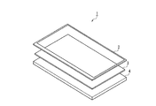
図1は本発明の第1の実施形態にかかる照明装置を用いた液晶表示装置の分解斜視図であり、図2は上記照明装置の分解斜視図である。図1において、本実施形態の液晶表示装置1は、前枠2と、この前枠2の後方に順次設けられた液晶パネル3及び本発明の照明装置4とを備えている。前枠2は、液晶パネル3の表示面を囲むように構成されている。液晶パネル3には、液晶層及び当該液晶層を挟むように設けられた一対の偏光板を有する(図示せず)、透過型の液晶表示素子が用いられている。また、液晶パネル3は、照明装置4からの平面状の光(照明光)が照射される表示部を構成しており、本実施形態では、液晶パネル3と照明装置4とが透過型の液晶表示装置1として一体化されている。[First Embodiment]
FIG. 1 is an exploded perspective view of a liquid crystal display device using the illumination device according to the first embodiment of the present invention, and FIG. 2 is an exploded perspective view of the illumination device. In FIG. 1, the liquid
また、照明装置4は、図2も参照して、当該照明装置4の発光面を囲むように構成された枠体5と、枠体5の後方に順次設置された光学シート6及び発光素子(光源)としての発光ダイオードを実装した光源基板としての発光ダイオード基板(以下、"LED基板"と略称する。)8を収容するシャーシ7を備えている。光学シート6には、偏光シート、プリズム(集光)シート、あるいは拡散シートなどの公知の光学シート材が必要に応じて含められており、この光学シート6によって照明装置4からの上記照明光の輝度上昇などが適宜行われて、液晶パネル3の表示性能を向上させるようになっている。
In addition, referring to FIG. 2, the illuminating device 4 also includes a frame 5 configured to surround the light emitting surface of the illuminating device 4, an optical sheet 6 and a light emitting element ( A
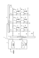
ここで、図3を参照して、液晶パネル3について具体的に説明する。
Here, the
図3は、図1に示した液晶パネルの要部構成を説明する図である。 FIG. 3 is a diagram for explaining a main configuration of the liquid crystal panel shown in FIG.
図3において、制御部9には、TV(受像機)あるいはPCなどの信号源(図示せず)を介して液晶表示装置1の外部から画像信号が入力されるようになっている。また、制御部9には、入力された画像信号を用いて、液晶パネル3に設けられた複数の画素を画素単位に駆動制御するパネル制御部10と、画像信号に含まれたフレーム単位の表示データを記憶可能に構成されたフレームメモリ11とが設けられている。パネル制御部10は、上記画像信号を基にソースドライバ12及びゲートドライバ13への各指示信号を生成するように構成されている。
In FIG. 3, an image signal is input to the
ソースドライバ12及びゲートドライバ13は、液晶パネル3の複数の画素を画素単位に駆動する駆動回路であり、ソースドライバ12及びゲートドライバ13には、複数の信号線S1〜SM(Mは、2以上の整数)及び複数の制御線G1〜GN(Nは、2以上の整数)がそれぞれ接続されている。これら信号線S1〜SM及び制御線G1〜GNは、マトリクス状に配列されており、当該マトリクス状に区画された各領域には、上記複数の各画素の領域が形成されている。これらの複数の画素には、赤色、緑色、及び青色の画素Pr、Pg、及びPbが含まれている。また、これら赤色、緑色、及び青色の画素Pr、Pg、及びPbは、例えばこの順番で、各制御線G1〜GNに平行に順次配設されている。
The
また、各制御線G1〜GNには、画素毎に設けられたスイッチング素子14のゲートが接続されている。一方、各信号線S1〜SMには、スイッチング素子17のソースが接続されている。また、各スイッチング素子14のドレインには、画素毎に設けられた画素電極15が接続されている。また、各画素では、共通電極16が液晶パネル3に設けられた上記液晶層を間に挟んだ状態で画素電極15に対向するように構成されている。そして、ゲートドライバ13は、パネル制御部10からの指示信号に基づいて、制御線G1〜GNに対して、対応するスイッチング素子14のゲートをオン状態にするゲート信号を順次出力する。一方、ソースドライバ12は、パネル制御部10からの指示信号に基づいて、表示画像(画像信号)の輝度(階調)に応じた電圧信号(階調電圧)を対応する信号線S1〜SMに出力する。これにより、液晶パネル3の液晶層での透過率が画素単位に変化し、照明装置4の発光面からの照明光によって、表示画像が表示面上に形成される。
The gates of the switching
次に、図4〜図7を参照して、照明装置4について具体的に説明する。 Next, the illumination device 4 will be described in detail with reference to FIGS.
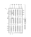
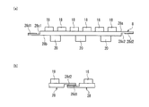
図4は上記照明装置4の要部構成を示す平面図である。図5は図4に示したLED基板8の構成を説明する図であり、図5(a)、図5(b)、及び図5(c)はそれぞれLED基板8の実装面8a、裏面8b、及び側面を示す図である。図6は図4に示したシャーシ7を示す斜視図である。図7(a)は図4のVIIa−VIIa線断面図であり、図7(b)は図4のVIIb−VIIb線断面図である。
FIG. 4 is a plan view showing a configuration of a main part of the illumination device 4. 5 is a diagram for explaining the configuration of the
図4に例示するように、照明装置4では、シャーシ7の内部に、同図4の横方向及び縦方向にそれぞれ沿って、3個及び6個の矩形状のLED基板8が設けられている。これらLED基板8は、後に詳述するように、上記横方向で隣接するLED基板8が互いに電気的に接続された状態で、シャーシ7に収容されている。すなわち、シャーシ7では、各々電気的に接続された3個のLED基板8からなる6列のLED基板群が構成されている。また、各LED基板8では、直線状に配列された複数、例えば6個の発光ダイオード18を含んだ発光ダイオード列が2列設けられており、合計12個の発光ダイオード18が設置されている。尚、照明装置4では、液晶パネル3の大きさや当該液晶パネル3で要求される輝度や表示品位等の表示性能などに応じて、LED基板8の設置数、発光ダイオード18の設置数、種類やサイズ等が適宜選択されている。
As illustrated in FIG. 4, in the lighting device 4, three and six
また、照明装置4には、例えばPWM調光を用いて、LED基板8の発光ダイオード18の点灯駆動を制御する照明制御部17が設けられている。この照明制御部17には、液晶表示装置1に付随するリモートコントローラ(図示せず)などから調光指示信号が入力されるように構成されている。そして、照明制御部17が、入力された調光指示信号に基づき、発光ダイオード18への供給電力を変更することによって、液晶パネル3に照射される照明光の輝度及び色度を適切に調整できるようになっている。
In addition, the illumination device 4 is provided with an illumination control unit 17 that controls lighting driving of the
具体的にいえば、図5に示すように、LED基板8の実装面8aには、上記複数の各発光ダイオード18として、例えば赤色(R)、緑色(G)、及び青色(B)の光をそれぞれ発光する赤色、緑色、及び青色の発光ダイオード18r、18g、18bを一体的に構成した、いわゆるスリーインワン(3in1)タイプのものが使用されている。また、実装面8a上では、図5(a)に示すように、上記横方向で互いに平行に2列の発光ダイオード列が設置されている。さらに、各発光ダイオード列では、6個の発光ダイオード18が所定の方向(横方向)に沿って、かつ、所定の間隔をおいて設けられている。これにより、照明装置4では、液晶パネル3への照明光に輝度ムラが発生するのを容易に防いで、当該照明装置4の発光品位を容易に向上できるようになっている。さらに、LED基板8では、発光ダイオード18r、18g、18bの各発光量が照明制御部17からの調光指示信号に応じた指示信号を基に変えられることで上記照明光の輝度及び色度が適切に変更される。
Specifically, as shown in FIG. 5, on the mounting
また、図5(b)に示すように、LED基板8では、その実装面8aの裏面8bに、発光ダイオード18で生じた熱を放熱する放熱部としての放熱パターン19が発光ダイオード18単位に設置されている。つまり、放熱パターン19は、対応する発光ダイオード18の真裏(真下)の位置に配置され、実装面8a側から裏面8b側にLED基板8内部に設けられたスルーホールなどを介して発光ダイオード18からの熱を実装面8a側から裏面8b側に効率よく伝えることができるように構成されている。
Further, as shown in FIG. 5B, in the
また、LED基板8の裏面8bでは、上記横方向に沿って、直線状に設けられた6個の放熱パターン19を各々含んだ2列の放熱パターン列単位に、放熱パターン19からシャーシ7側に熱を伝える伝熱部材としての伝熱テープ21が取り付けられるようになっている。伝熱テープ21には、例えばアクリル樹脂などの高い熱伝導率を有する帯状の合成樹脂シールが使用されており、伝熱テープ21は、放熱パターン列を覆うように設けられている。そして、伝熱テープ21は、発光ダイオード18で生じた熱をシャーシ7側に伝えて、外部に放熱させる(詳細は後述。)。
Further, on the
また、LED基板8の裏面8bには、2列の放熱パターン列の間、すなわち実装面8a上に実装された2列の発光ダイオード列の間に配置されるように、例えば3個のLEDドライバ20が実装されている。これらの各LEDドライバ20は、発光ダイオード18を駆動する駆動回路素子であり、発光ダイオード18に対して定電流を供給する定電流回路、抵抗素子、コンデンサなどの所定の電子部品を集積化したICによって構成されている。また、各LEDドライバ20は、LED基板8内部に設けられたスルーホールなどを介して4個の発光ダイオード18に電気的に接続されており、照明制御部17からの指示信号に基づき接続された4個の発光ダイオード18を個別に駆動するようになっている。
Further, for example, three LED drivers are disposed on the
さらに、LED基板8の裏面8bでは、互いに平行な左端部及び右端部に、端子部8c1及び8c2がそれぞれ設けられている。これらの端子部8c1、8c2は、図示を省略したプリント回路を介してLEDドライバ20に電気的に接続されている。また、端子部8c1、8c2は、スルーホールなどを介して直接的、あるいはLEDドライバ20を介して間接的に発光ダイオード18に電気的に接続されている。そして、LED基板8では、端子部8c1、8c2を介して、照明制御部17からの指示信号が入力されるとともに、図示を省略した電源から電力が供給されるように構成されている。
Further, on the
また、LED基板8では、図5(c)に示すように、発光ダイオード18及びLEDドライバ20がそれぞれ実装面8a及び裏面8bから突出するように設けられている。これらの発光ダイオード18及びLEDドライバ20は、対応する実装面8a及び裏面8b上に設けられたプリント回路に対して、ハンダ付けを用いて実装されて固定されている。
In the
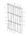
シャーシ7には、例えばアルミニウム等の熱伝導率の高い金属が使用されており、発光ダイオード18で生じた熱を外部に放熱するようになっている。具体的にいえば、図6に示すように、シャーシ7は、当該シャーシ7の側壁部を構成する額縁状の枠体7aと、枠体7aの一端側(下側)を閉塞するように当該枠体7aに一体的に設けられた平板状の底板7bとを備えている。また、シャーシ7には、LED基板8を支持する支持部7c1、7c2と、上記横方向で隣接する2つのLED基板8を互いに電気的に接続する接続部7dと、LED基板8と照明制御部17及び上記電源とを電気的に接続する接続部7eとが設けられている。また、シャーシ7には、上記横方向と平行に設けられた6条の溝7f及び上記縦方向と平行に設けられた3条の溝7gが設けられており、12個の接続部7d及び6個の接続部7eが溝7f、7gの交差部でシャーシ7の底面7bに一体的に設置されている。
The
詳細には、シャーシ7の底板7bは、所望の剛性(強度)を有するように厚さ寸法や材質などが決定されており、当該底板7b上に長方形状の支持部7c1、7c2が固定されている。また、支持部7c1では、その上記発光面側(上側)の表面積が支持部7c2の同表面積のほぼ2倍とされており、支持部7c1は、縦方向で隣接して設置される2つのLED基板8を支持するように構成されている。一方、最上段及び最下段の支持部7c2は、最上行及び最下行のLED基板8をそれぞれ支持するようになっている。さらに、シャーシ7では、溝7fが縦方向で隣接する2つの支持部7c1の間及び縦方向で隣接する支持部7c1と支持部7c2との間に形成されており、LEDドライバ20が溝7f内に配置された状態で、LED基板8は、対応する支持部7c1、7c2にて支持されるようになっている。
Specifically, the thickness and material of the
すなわち、図7(a)に例示するように、LED基板8では、LEDドライバ20が溝7f内に収納された状態で、伝熱テープ21を介在させて支持部7c1、7c2上に置かれて支持されている。また、この伝熱テープ21には、熱伝導性だけでなく弾性が付与されており、伝熱テープ21は、LED基板8の放熱パターン19及び支持部7c1、7c2との各密着性を向上させるように構成されている。さらに、伝熱テープ21では、その両面、すなわちLED基板8側の表面及び支持部7c1、7c2側の表面に接着性が付与されており、これらの各表面に当接するLED基板8の裏面8b及び支持部7c1、7c2の表面と確実に、かつ、安定した状態で面接触するようになっている。
That is, as illustrated in FIG. 7A, in the
以上のように、伝熱テープ21がLED基板8とシャーシ7との各密着性を高めつつ、これらLED基板8とシャーシ7との各間で確実に、かつ、安定した状態で面接触するように構成されているので、本実施形態の照明装置4では、伝熱テープ21によるLED基板8側からシャーシ側への熱伝導の効率が低下するのを極力防止することができる。この結果、本実施形態の照明装置4では、発光ダイオード18で生じた熱を、放熱パターン19、伝熱テープ21、支持部7c1、7c2、及び底板7bを経てシャーシ7の外部に迅速に、かつ、より効率よく放熱させることができる。従って、本実施形態の照明装置4では、周囲温度の変動に起因して発光ダイオード18の発光量が変動するのを防ぐことができ、優れた発光品位の照明装置4をより容易に構成することができる。
As described above, the
尚、上記の説明以外に、伝熱シート21を用いることなく、LED基板8の放熱パターン19とシャーシ7の支持部7c1、7c2とを直接的に接触させる構成でもよい。また、伝熱シート21の代わりに、硬化後にゴム弾性体となる熱伝導性を有する接着剤を使用することもできる。また、シャーシ7の底板7bに、例えばヒートシンクを設置して、当該シャーシ7の放熱能力を高めたり、ファンや水(冷却媒体)が流通されるウォータジャケット等の発光ダイオードの熱を強制冷却可能な放熱機構を底板7bの背面側に設けたりしてもよい。
In addition to the above description, a configuration in which the
また、シャーシ7では、12個の各接続部7dが上記横方向で隣接する2つのLED基板8の間に配置されるように、シャーシ7の底板7bに一体的に取り付けられている。すなわち、図6に示すように、6個の接続部7dが上記縦方向と平行に設けられた3条の溝7gのうち、同図の左側及び中央の溝7gの内部で所定の間隔をおいて、直線状に設けられている。
In the
また、これらの各接続部7dには、図7(b)に例示するように、LED基板8の端子部8c2に接して導通する金属膜7d1と、ゴム材などの弾性体を用いて構成されるとともに、金属膜7d1に一体化されて当該金属膜7d1を支持する支持体7d2とが設けられている。また、支持体7d2は、ネジあるいは接着剤など固定手段(図示せず)によって底板7bに取り付けられており、各接続部7dは、弾性変形可能な状態で、シャーシ7の底板7bに一体的に取り付けられている。さらに、各接続部7dでは、金属膜7d1上に横方向で隣接する2つのLED基板8の端子部8c1、8c2が載置されることで、これらのLED基板8を互いに電気的に接続可能に構成されている。
Further, as illustrated in FIG. 7B, each of these
また、6個の各接続部7eは、図6の右側の溝7gの内部で所定の間隔をおいて、直線状に設けられている。また、これらの各接続部7eは、接続部7dと同様に、枠体7a及び底板7bに対し電気的に絶縁された状態で、かつ、底板7bに対して弾性変形可能な状態で、シャーシ7の底板7bに一体的に取り付けられている。また、各接続部7eには、一端部が照明制御部17及び上記電源に接続されたFPC(図示せず)の他端部が電気的に接続されており、LED基板8側への上記指示信号の出力及び電力供給が行われるようになっている。
Each of the six
以上のように構成された本実施形態の照明装置4では、複数の各LED基板(光源基板)8において、発光ダイオード(発光素子)18及びLEDドライバ(駆動回路素子)20に電気的に接続された端子部8c1、8c2を、実装面8aの裏面8b側で互いに平行な左端部及び右端部にそれぞれ設けている。また、本実施形態の照明装置4では、LED基板8の端子部8c1、8c2に電気的に接続可能な接続部7dをシャーシ7に設置している。これにより、本実施形態の照明装置4では、上記従来例と異なり、発光ダイオード18の設置数の増加に伴って、必要なLED基板8を増加させるときでも、LED基板8毎に信号線や電力線などの電気配線を設けることなく、複数のLED基板8を電気的に接続することができる。従って、本実施形態の照明装置4では、液晶表示装置1の大画面化などに応じて、発光ダイオード18の設置数を増加させるときでも、上記従来例と異なり、電気配線の配線作業を簡略化することができる。さらに、本実施形態では、電気配線の設置スペースを極力小さくすることができることから、構造簡単でコンパクトな照明装置4を構成することができる。
In the illuminating device 4 of the present embodiment configured as described above, each of the plurality of LED substrates (light source substrates) 8 is electrically connected to a light emitting diode (light emitting element) 18 and an LED driver (drive circuit element) 20. The terminal portions 8c1 and 8c2 are provided at the left end portion and the right end portion that are parallel to each other on the
また、本実施形態では、上記のように、発光ダイオード18の設置数を増加させる場合でも、電気配線の配線作業を簡略化することができる構造簡単でコンパクトな照明装置4が用いられているので、高輝度で薄型化された高性能な液晶表示装置1を容易に構成することが可能となる。
Further, in the present embodiment, as described above, the lighting device 4 having a simple structure and compactness that can simplify the wiring work of the electric wiring even when the number of the
また、本実施形態の照明装置4では、隣接する2つの一方のLED基板8の端子部8c1と他方のLED基板8の端子部8c2とを接続部7dに載置することにより、これらのLED基板8を電気的に接続することができる。この結果、本実施形態では、組立性に優れた照明装置4を構成することができる。また、シャーシ7に設置された接続部7dを使用しているので、複数の各LED基板8の位置決め作業を容易に行うことが可能となって、LED基板8のシャーシ7への組付作業を簡単に、かつ高精度に行うことができる。この結果、本実施形態では、生産性に優れた照明装置4、及び液晶表示装置1を構成することができる。
Moreover, in the illuminating device 4 of this embodiment, these LED boards are mounted by mounting the terminal part 8c1 of two adjacent one
しかも、本実施形態の照明装置4では、FPCなどの電気配線や専用のコネクタなどを用いることなく、LED基板8どうしを電気的に接続しているので、図4に例示したように、デッドスペースを生じることなく、シャーシ7に複数のLED基板8を収容させることができ、照明装置4が大型化するのを容易に防ぐことができる。
In addition, in the illumination device 4 of the present embodiment, the
また、本実施形態では、接続部7d、7eは弾性変形可能な状態でシャーシ7に一体的に設けられているので、端子部8c1、8c2との電気的な接続をより確実な状態で行わせることができる。また、各接続部7d、7eがシャーシ7に対し弾性変形可能とされているので、上記ネジなどの固定手段によってLED基板8をシャーシ7に固定するときでも、当該接続部7d、7eを介して接続されるLED基板8のシャーシ7の底板7bからの高さ寸法を容易に所定値に合わせることが可能となる。この結果、本実施形態の照明装置4では、LED基板8とシャーシ7との組付精度を簡単に高めることができる。
In the present embodiment, since the
尚、上記の説明以外に、接続部7d、7eに代えて、シャーシ7に対し、着脱可能に構成された接続部材を使用することもできる。
In addition to the above description, a connecting member configured to be detachable from the
[第2の実施形態]
図8は本発明の第2の実施形態にかかる照明装置に用いられるLED基板の構成を説明する図であり、図8(a)及び図8(b)はそれぞれLED基板の実装面及び裏面を示す図である。図9(a)は図8に示したLED基板の側面を示す図であり、図9(b)は2つの同LED基板の接続状態を説明する図である。図において、本実施形態と上記第1の実施形態との主な相違点は、LED基板の実装面側及び裏面側に端子部を設けて、接続部を介在させることなく、2つのLED基板を互いに電気的に接続可能に構成した点である。なお、上記第1の実施形態と共通する要素については、同じ符号を付して、その重複した説明を省略する。[Second Embodiment]
FIG. 8 is a diagram for explaining the configuration of the LED substrate used in the illumination device according to the second embodiment of the present invention. FIGS. 8A and 8B show the mounting surface and the back surface of the LED substrate, respectively. FIG. Fig.9 (a) is a figure which shows the side surface of the LED board shown in FIG. 8, FIG.9 (b) is a figure explaining the connection state of two same LED boards. In the figure, the main difference between this embodiment and the first embodiment is that the LED board is provided with terminal portions on the mounting surface side and the back surface side, and the two LED substrates are connected without interposing a connection portion. It is the point which comprised so that electrical connection was possible mutually. In addition, about the element which is common in the said 1st Embodiment, the same code | symbol is attached | subjected and the duplicate description is abbreviate | omitted.
つまり、図8(a)に例示するように、本実施形態の発光ダイオード基板(LED基板)28では、実装面28a側の左端部に段差部28c1が形成されており、この段差部28c1には、発光ダイオード18及びLEDドライバ20に電気的に接続された端子部28d1が設けられている。
That is, as illustrated in FIG. 8A, in the light emitting diode substrate (LED substrate) 28 of the present embodiment, a step portion 28c1 is formed at the left end portion on the mounting
一方、図8(b)に例示するように、LED基板28では、裏面28b側の右端部に段差部28c2が形成されており、この段差部28c2には、発光ダイオード18及びLEDドライバ20に電気的に接続された端子部28d2が設けられている。
On the other hand, as illustrated in FIG. 8B, in the
また、図9(a)に示すように、段差部28c1、28c2は、それぞれ実装面28a及び裏面28bを断面矩形状に切り欠くことによって形成されている。さらに、本実施形態では、隣接する2つのLED基板28が電気的に接続される場合、図9(b)に例示するように、左側のLED基板28の端子部28d2と右側のLED基板28の端子部28d2が直接的に接続されるようになっている。また、このように2つのLED基板28が接続されて、上記固定手段にてシャーシ7に取り付けられた場合、これらの各LED基板28では、第1の実施形態のものと同様に、底板7bからの高さ寸法が所定値に合わせられており、各LED基板28の上記発光面までの離間距離が均一とされている。
Further, as shown in FIG. 9A, the step portions 28c1 and 28c2 are formed by cutting out the mounting
以上の構成により、本実施形態では、上記第1の実施形態と同様な作用・効果を奏することができる。また、本実施形態では、接続部を使用することなく、複数のLED基板28が直接的に電気的に接続されているので、照明装置4、ひいては液晶表示装置1の部品点数を削減することができるとともに、構造簡単な照明装置4をより容易に構成することができる。
With the above configuration, the present embodiment can achieve the same operations and effects as the first embodiment. Moreover, in this embodiment, since the some
尚、上記の実施形態はすべて例示であって制限的なものではない。本発明の技術的範囲は特許請求の範囲によって規定され、そこに記載された構成と均等の範囲内のすべての変更も本発明の技術的範囲に含まれる。 The above embodiments are all illustrative and not restrictive. The technical scope of the present invention is defined by the claims, and all modifications within the scope equivalent to the configurations described therein are also included in the technical scope of the present invention.
例えば、上記の説明では、本発明を透過型の液晶表示装置に適用した場合について説明したが、本発明の照明装置はこれに限定されるものではなく、光源の光を利用して、画像、文字などの情報を表示する非発光型の表示部を備えた各種表示装置に適用することができる。具体的には、半透過型の液晶表示装置、あるいは上記液晶パネルをライトバルブに用いたリアプロジェクションなどの投写型表示装置に本発明の照明装置を好適に用いることができる。 For example, in the above description, the case where the present invention is applied to a transmissive liquid crystal display device has been described. However, the lighting device of the present invention is not limited to this, and the image, The present invention can be applied to various display devices including a non-light emitting display unit that displays information such as characters. Specifically, the illumination device of the present invention can be suitably used for a transflective liquid crystal display device or a projection display device such as a rear projection using the liquid crystal panel as a light valve.
また、上記の説明以外に、本発明は、レントゲン写真に光を照射するシャウカステンあるいは写真ネガ等に光を照射して視認をし易くするためのライトボックスや、看板や駅構内の壁面などに設置される広告等をライトアップする発光装置の照明装置として好適に用いることができる。 In addition to the above explanation, the present invention is installed on a light box for illuminating X-ray film or photographic negatives for irradiating light to make it easy to see, or on a signboard or a wall in a station. It can be suitably used as a lighting device for a light emitting device that illuminates advertisements and the like.
また、上記の説明では、直線状に並べられた6個の発光ダイオードを含んだ発光ダイオード列を2列設けたLED基板を使用するとともに、直線状に配列され、かつ、電気的に接続された各々3個のLED基板からなる6列のLED基板群を用いた場合について説明した。しかしながら、本発明は複数の発光素子が実装面上に実装された光源基板を複数備えるとともに、これら複数の光源基板が、隣接する光源基板が互いに電気的に接続された状態で、設けられているものであれば、光源基板の構成(発光素子の設置数や種類を含む。)、光源基板の設置数や接続方法などは上記のものに何等限定されない。 In the above description, an LED substrate having two light emitting diode rows including six light emitting diodes arranged in a straight line is used, and the LED substrates are arranged in a straight line and are electrically connected. The case of using six rows of LED substrate groups each consisting of three LED substrates has been described. However, the present invention includes a plurality of light source substrates on which a plurality of light emitting elements are mounted on a mounting surface, and the plurality of light source substrates are provided in a state where adjacent light source substrates are electrically connected to each other. If it is a thing, the structure of a light source board | substrate (including the installation number and kind of light emitting element), the installation number of a light source board | substrate, a connection method, etc. will not be limited to the above thing at all.
但し、上記の各実施形態のように、光源基板において、互いに平行な2つの端部に発光素子に電気的に接続される端子部を設けて、接続部を介在させたり、異なる光源基板の端子部を互いに直接的に接続したりする場合の方が、FPCなどの電気配線や専用のコネクタなどを設けることなく、2つの光源基板を確実に電気的に接続することができる点で好ましい。 However, as in each of the above embodiments, in the light source substrate, a terminal portion that is electrically connected to the light emitting element is provided at two end portions parallel to each other, and the connection portion is interposed, or a terminal of a different light source substrate The case where the parts are directly connected to each other is preferable in that the two light source substrates can be reliably electrically connected without providing electric wiring such as FPC or a dedicated connector.
また、上記の各実施形態のように、発光素子に発光ダイオードを使用する場合の方が、消費電力が少なく、優れた環境性をもつ照明装置を容易に構成することができる点での好ましい。 Further, as in each of the embodiments described above, the case where a light emitting diode is used as the light emitting element is preferable in that an illumination device with low power consumption and excellent environmental characteristics can be easily configured.
また、上記の説明では、RGBの発光ダイオードを一体化した複数の3in1タイプの発光ダイオードを使用した場合について説明したが、本発明の発光ダイオードはこれに限定されるものではなく、R、G、Bそれぞれ単色個別の発光ダイオードを用いたり、白色光の発する白色(W)の発光ダイオードを用いたり、RGBWや、GRGBなど4つの発光ダイオードを一体化した、いわゆるフォーインワン(4in1)タイプの発光ダイオードを適用したりすることもできる。また、RGBW以外の色の発光ダイオードを追加することもできる。この場合には、液晶パネルの画素構成にも色の追加が必要となるが、より広範囲の色を再現できるようになる。具体的な追加する色としては、例えばイエロー、マゼンダ等がある。 In the above description, the case where a plurality of 3-in-1 type light emitting diodes in which RGB light emitting diodes are integrated has been described. However, the light emitting diode of the present invention is not limited to this, and R, G, Each B uses a single color light emitting diode, a white (W) light emitting diode that emits white light, or a so-called four-in-one (4 in 1) type light emitting diode that integrates four light emitting diodes such as RGBW and GRGB. Can also be applied. Further, light emitting diodes of colors other than RGBW can be added. In this case, it is necessary to add a color to the pixel configuration of the liquid crystal panel, but a wider range of colors can be reproduced. Specific colors to be added include, for example, yellow and magenta.
但し、上記の各実施形態のように、発光色が互いに異なるとともに、白色光に混色可能な複数種類(例えば、RGB)の発光ダイオードを用いる場合の方が、白色の発光ダイオードのみで構成する場合に比べて、複数種類の各発光ダイオードの発光色に対応した色純度を向上できる点で好ましい。さらには、優れた発光品位を有する照明装置、ひいては優れた表示品位を有する表示装置を容易に構成することができる点でも好ましい。 However, as in the above-described embodiments, the case where a plurality of types (for example, RGB) of light emitting diodes that have different emission colors and can be mixed with white light is composed of only white light emitting diodes. Compared to the above, it is preferable in that the color purity corresponding to the emission color of each of the plural types of light emitting diodes can be improved. Furthermore, it is also preferable in that an illumination device having excellent light emission quality, and in turn, a display device having excellent display quality can be easily configured.
また、上記の説明では、直下型の照明装置を構成した場合について説明したが、本発明はこれに限定されるものではなく、例えば照明装置の発光面の下方に単一の導光板を設けるとともに、当該導光板を囲んだ四辺の少なくとも一辺に対して、平行に複数の光源基板を配列したエッジライト型の照明装置や発光素子毎に導光板を設けたタンデム型などの他の形式の照明装置にも適用することができる。また、光源基板の実装面上に導光板等の光学部材を設置する必要があるタンデム型などの照明装置に適用する場合でも、図5に示したように、本発明では、光源基板の実装面側に上記コネクタなどの発光素子以外の電気部品などの設置を省略しているので、上記光学部材の設置を容易に行えたり、照明装置の薄型化を容易に図れたりすることができる。 In the above description, the case where the direct type illumination device is configured has been described. However, the present invention is not limited to this. For example, a single light guide plate is provided below the light emitting surface of the illumination device. Other types of illumination devices such as an edge light type illumination device in which a plurality of light source substrates are arranged in parallel to at least one of the four sides surrounding the light guide plate, and a tandem type in which a light guide plate is provided for each light emitting element It can also be applied to. Further, even when applied to a tandem type lighting device in which an optical member such as a light guide plate needs to be installed on the mounting surface of the light source substrate, as shown in FIG. Since installation of electrical components other than light emitting elements such as the connector is omitted on the side, the optical member can be easily installed, and the lighting device can be easily made thin.
また、上記の説明以外に、本発明は例えば液晶パネルでの情報表示に応じて、複数の発光素子を順次発光させるバックライトスキャン駆動を実施可能に構成された照明装置や、複数の照明エリアが液晶パネル側の表示エリアに対応して設定されるとともに、照明エリア内の発光素子を照明エリア単位に発光させるエリアアクティブバックライト駆動を実施可能に構成された照明装置にも適用することができる。 In addition to the above description, the present invention includes, for example, an illumination device configured to be able to perform backlight scan driving that sequentially emits a plurality of light emitting elements according to information display on a liquid crystal panel, and a plurality of illumination areas. The present invention can also be applied to an illuminating device that is set corresponding to a display area on the liquid crystal panel side and that can perform area active backlight driving in which light emitting elements in the illumination area emit light in units of illumination areas.
本発明は、発光素子の設置数を増加させる場合でも、電気配線の配線作業を簡略化することができる構造簡単でコンパクトな照明装置、及びこれを用いた高性能な表示装置に対して有用である。 INDUSTRIAL APPLICABILITY The present invention is useful for a simple and compact lighting device that can simplify the wiring work of electric wiring even when the number of installed light emitting elements is increased, and a high-performance display device using the same. is there.
Claims (5)
前記光源基板を収容するシャーシを備えるとともに、
前記光源基板の実装面には、複数の前記発光素子が設けられ、
前記光源基板には、前記発光素子に電気的に接続される2つの端子部が前記実装面の裏面側で当該光源基板の互いに平行な2つの端部にそれぞれ設けられ、
前記シャーシには、前記光源基板に設けられた前記端子部に電気的に接続される接続部が設置され、
複数の前記光源基板が、隣接する前記光源基板が互いに電気的に接続された状態で、設けられ、
前記接続部は、弾性変形可能な状態で、前記シャーシに一体的に設けられている、
ことを特徴とする照明装置。A lighting device including a light emitting element and a light source substrate having a mounting surface on which the light emitting element is mounted,
With a chassis that houses the light source substrate,
The mounting surface of the light source substrate is provided with a plurality of the light emitting elements,
In the light source substrate, two terminal portions that are electrically connected to the light emitting element are respectively provided at two parallel end portions of the light source substrate on the back side of the mounting surface,
The chassis is provided with a connecting portion that is electrically connected to the terminal portion provided on the light source substrate,
A plurality of the light source substrates are provided in a state where the adjacent light source substrates are electrically connected to each other,
The connecting portion is provided integrally with the chassis in an elastically deformable state.
A lighting device characterized by that.
前記表示部には、請求項1〜4のいずれか1項に記載の照明装置からの光が照射されることを特徴とする表示装置。A display device including a display unit,
Wherein the display unit includes a display device characterized by light from the illumination device according to any one of claims 1-4 is irradiated.
Priority Applications (1)
| Application Number | Priority Date | Filing Date | Title |
|---|---|---|---|
| JP2009525295A JP4977207B2 (en) | 2007-07-27 | 2008-02-20 | LIGHTING DEVICE AND DISPLAY DEVICE USING THE SAME |
Applications Claiming Priority (4)
| Application Number | Priority Date | Filing Date | Title |
|---|---|---|---|
| JP2007196095 | 2007-07-27 | ||
| JP2007196095 | 2007-07-27 | ||
| JP2009525295A JP4977207B2 (en) | 2007-07-27 | 2008-02-20 | LIGHTING DEVICE AND DISPLAY DEVICE USING THE SAME |
| PCT/JP2008/052863 WO2009016853A1 (en) | 2007-07-27 | 2008-02-20 | Lighting equipment and display device using the same |
Publications (2)
| Publication Number | Publication Date |
|---|---|
| JPWO2009016853A1 JPWO2009016853A1 (en) | 2010-10-14 |
| JP4977207B2 true JP4977207B2 (en) | 2012-07-18 |
Family
ID=40304095
Family Applications (1)
| Application Number | Title | Priority Date | Filing Date |
|---|---|---|---|
| JP2009525295A Expired - Fee Related JP4977207B2 (en) | 2007-07-27 | 2008-02-20 | LIGHTING DEVICE AND DISPLAY DEVICE USING THE SAME |
Country Status (6)
| Country | Link |
|---|---|
| US (1) | US20100202130A1 (en) |
| EP (1) | EP2154422B1 (en) |
| JP (1) | JP4977207B2 (en) |
| CN (1) | CN101680624B (en) |
| AT (1) | ATE513162T1 (en) |
| WO (1) | WO2009016853A1 (en) |
Families Citing this family (8)
| Publication number | Priority date | Publication date | Assignee | Title |
|---|---|---|---|---|
| US20110109834A1 (en) * | 2008-07-07 | 2011-05-12 | Sharp Kabushiki Kaisha | Frame set, lighting device, and liquid crystal display device |
| JP5478791B2 (en) * | 2009-07-17 | 2014-04-23 | 古河電池株式会社 | Assembled battery |
| JP2011053238A (en) * | 2009-08-31 | 2011-03-17 | Hitachi Consumer Electronics Co Ltd | Liquid crystal display apparatus and back light apparatus |
| WO2012081185A1 (en) * | 2010-12-16 | 2012-06-21 | パナソニック株式会社 | Backlight device and liquid-crystal display device |
| JP5738709B2 (en) * | 2011-07-29 | 2015-06-24 | シャープ株式会社 | LED substrate, lighting device and display device |
| GB2502777A (en) * | 2012-06-04 | 2013-12-11 | Metrolight Ltd | Modular LED lighting fixture |
| AT14221U1 (en) * | 2014-05-19 | 2015-06-15 | Tridonic Gmbh & Co Kg | Bulb with LED and method of assembly |
| JP6454114B2 (en) * | 2014-09-26 | 2019-01-16 | 東芝映像ソリューション株式会社 | Video display device |
Citations (7)
| Publication number | Priority date | Publication date | Assignee | Title |
|---|---|---|---|---|
| JP2002163912A (en) * | 2000-11-28 | 2002-06-07 | Harison Toshiba Lighting Corp | Light emitting equipment system and light emitting diode array |
| JP2006301209A (en) * | 2005-04-19 | 2006-11-02 | Sony Corp | Backlight unit and liquid crystal display device |
| JP2007027114A (en) * | 2005-07-14 | 2007-02-01 | Samsung Electronics Co Ltd | Backlight unit and liquid crystal display device including above |
| JP2007027745A (en) * | 2005-07-15 | 2007-02-01 | Samsung Electro Mech Co Ltd | Surface light source using led and lcd backlight unit having the same |
| JP2007066879A (en) * | 2005-08-26 | 2007-03-15 | Paikomu Corp | Backlight device and control method |
| JP2007087662A (en) * | 2005-09-20 | 2007-04-05 | Toyoda Gosei Co Ltd | Light source unit and light source apparatus using the same |
| JP2007109447A (en) * | 2005-10-11 | 2007-04-26 | E Image Technology Kk | Planar lighting source |
Family Cites Families (20)
| Publication number | Priority date | Publication date | Assignee | Title |
|---|---|---|---|---|
| GB8807758D0 (en) * | 1988-03-31 | 1988-05-05 | Consumerville Ltd | Decorative lighting system |
| JP4696469B2 (en) | 2004-04-30 | 2011-06-08 | ソニー株式会社 | Backlight device |
| JP4442304B2 (en) | 2004-04-30 | 2010-03-31 | ソニー株式会社 | Light emitting unit heat dissipation device and backlight device |
| JP2005339881A (en) | 2004-05-25 | 2005-12-08 | Hitachi Displays Ltd | Lighting device, lighting module, and liquid crystal display |
| KR20060134375A (en) * | 2005-06-22 | 2006-12-28 | 삼성전자주식회사 | Backlight assembly and display device provided with the same |
| KR101134302B1 (en) * | 2005-06-30 | 2012-04-13 | 엘지디스플레이 주식회사 | cover bottom for liquid crystal display device, LED back light assembly and liquid crystal display module using thereof |
| TWI333576B (en) * | 2005-08-17 | 2010-11-21 | Au Optronics Corp | Bottom lighting module |
| EP1760392A1 (en) * | 2005-08-29 | 2007-03-07 | Patent-Treuhand-Gesellschaft für elektrische Glühlampen mbH | A mounting structure for LED lighting systems |
| US7959325B2 (en) * | 2005-11-18 | 2011-06-14 | Cree, Inc. | Solid state lighting units and methods of forming solid state lighting units |
| JP2007311561A (en) * | 2006-05-18 | 2007-11-29 | Showa Denko Kk | Display unit, light emitting device, and solid-state light emitting element substrate |
| US20080049164A1 (en) * | 2006-08-22 | 2008-02-28 | Samsung Electronics Co., Ltd., | Backlight assembly, manufacturing method thereof, and liquid crystal display device |
| KR100844757B1 (en) * | 2006-08-24 | 2008-07-07 | 엘지이노텍 주식회사 | Lighting device and display apparatus using its |
| KR101277750B1 (en) * | 2006-10-19 | 2013-06-24 | 삼성디스플레이 주식회사 | Reflector member, backlight assembly and dislplay apparatus having the same |
| US7607790B2 (en) * | 2006-12-18 | 2009-10-27 | Hong Kong Applied Science And Technology Research Institute Co., Ltd. | Backlighting apparatus and manufacturing process |
| CN201083924Y (en) * | 2007-06-22 | 2008-07-09 | 群康科技(深圳)有限公司 | Backlight module group and LCD |
| KR100875703B1 (en) * | 2007-06-29 | 2008-12-23 | 알티전자 주식회사 | Back light unit of direct type |
| KR101123541B1 (en) * | 2007-07-06 | 2012-03-12 | 엘지디스플레이 주식회사 | Flat-light Unit and Liquid Crystal Display Device with the same |
| KR101394007B1 (en) * | 2007-09-11 | 2014-05-13 | 엘지이노텍 주식회사 | Light unit and display apparatus having thereof |
| KR101421626B1 (en) * | 2008-01-09 | 2014-07-22 | 삼성디스플레이 주식회사 | Light source unit and backlight unit and liquid crystal display having the same |
| US8537302B2 (en) * | 2008-06-11 | 2013-09-17 | Manufacturing Resources International, Inc. | Liquid crystal display assembly comprising an LED backlight assembly and a movable element placed behind the LED backlight assembly having a hinge to allow access to a rear portion of the LED backlight assembly |
-
2008
- 2008-02-20 WO PCT/JP2008/052863 patent/WO2009016853A1/en active Application Filing
- 2008-02-20 JP JP2009525295A patent/JP4977207B2/en not_active Expired - Fee Related
- 2008-02-20 AT AT08711669T patent/ATE513162T1/en not_active IP Right Cessation
- 2008-02-20 EP EP08711669A patent/EP2154422B1/en not_active Not-in-force
- 2008-02-20 CN CN2008800179866A patent/CN101680624B/en not_active Expired - Fee Related
- 2008-02-20 US US12/670,758 patent/US20100202130A1/en not_active Abandoned
Patent Citations (7)
| Publication number | Priority date | Publication date | Assignee | Title |
|---|---|---|---|---|
| JP2002163912A (en) * | 2000-11-28 | 2002-06-07 | Harison Toshiba Lighting Corp | Light emitting equipment system and light emitting diode array |
| JP2006301209A (en) * | 2005-04-19 | 2006-11-02 | Sony Corp | Backlight unit and liquid crystal display device |
| JP2007027114A (en) * | 2005-07-14 | 2007-02-01 | Samsung Electronics Co Ltd | Backlight unit and liquid crystal display device including above |
| JP2007027745A (en) * | 2005-07-15 | 2007-02-01 | Samsung Electro Mech Co Ltd | Surface light source using led and lcd backlight unit having the same |
| JP2007066879A (en) * | 2005-08-26 | 2007-03-15 | Paikomu Corp | Backlight device and control method |
| JP2007087662A (en) * | 2005-09-20 | 2007-04-05 | Toyoda Gosei Co Ltd | Light source unit and light source apparatus using the same |
| JP2007109447A (en) * | 2005-10-11 | 2007-04-26 | E Image Technology Kk | Planar lighting source |
Also Published As
| Publication number | Publication date |
|---|---|
| US20100202130A1 (en) | 2010-08-12 |
| EP2154422B1 (en) | 2011-06-15 |
| EP2154422A1 (en) | 2010-02-17 |
| ATE513162T1 (en) | 2011-07-15 |
| CN101680624B (en) | 2012-09-26 |
| EP2154422A4 (en) | 2010-06-02 |
| JPWO2009016853A1 (en) | 2010-10-14 |
| WO2009016853A1 (en) | 2009-02-05 |
| CN101680624A (en) | 2010-03-24 |
Similar Documents
| Publication | Publication Date | Title |
|---|---|---|
| JP4977206B2 (en) | LIGHTING DEVICE AND DISPLAY DEVICE USING THE SAME | |
| KR101308752B1 (en) | Liquid crystal display device | |
| JP4977207B2 (en) | LIGHTING DEVICE AND DISPLAY DEVICE USING THE SAME | |
| KR101255833B1 (en) | Liquid crystal display device | |
| KR101189135B1 (en) | Liquid Crystal Display device module | |
| US8083372B2 (en) | Illumination system, electro-optic device, and electronic apparatus | |
| KR101035502B1 (en) | liquid crystal display module using LED | |
| KR20120012150A (en) | Liquid crystal display device | |
| KR20100033726A (en) | Light source module and display device having the same | |
| JP4113832B2 (en) | Planar light source device and liquid crystal display device using the same | |
| WO2011043094A1 (en) | Lighting device and display device | |
| KR101687783B1 (en) | Liquid crystal display device | |
| WO2012026162A1 (en) | Lighting apparatus, display apparatus, and television receiver apparatus | |
| KR101770640B1 (en) | Backlight unit and liquid crystal display device including the same | |
| WO2018193695A1 (en) | Illumination device, display device, and television receiving device | |
| KR101990528B1 (en) | LED assembly and liquid crystal display device using the same | |
| KR20120123921A (en) | Liquid crystal display device | |
| KR101252880B1 (en) | Liquid crystal display divice | |
| WO2011040089A1 (en) | Lighting device and display device | |
| WO2010113349A1 (en) | Led illuminating device, and display device provided with the led illuminating device | |
| KR20080002319A (en) | Backlight assembly and liquid crystal display device having the same | |
| CN112349212A (en) | Display module, display panel and display device | |
| WO2013008779A1 (en) | Backlight device, display device, and television receiver | |
| KR20160038933A (en) | Liquid crystal display device module | |
| KR20160092532A (en) | Liquid crystal display device |
Legal Events
| Date | Code | Title | Description |
|---|---|---|---|
| A131 | Notification of reasons for refusal |
Free format text: JAPANESE INTERMEDIATE CODE: A131 Effective date: 20111018 |
|
| A521 | Request for written amendment filed |
Free format text: JAPANESE INTERMEDIATE CODE: A523 Effective date: 20111117 |
|
| TRDD | Decision of grant or rejection written | ||
| A01 | Written decision to grant a patent or to grant a registration (utility model) |
Free format text: JAPANESE INTERMEDIATE CODE: A01 Effective date: 20120322 |
|
| A01 | Written decision to grant a patent or to grant a registration (utility model) |
Free format text: JAPANESE INTERMEDIATE CODE: A01 |
|
| A61 | First payment of annual fees (during grant procedure) |
Free format text: JAPANESE INTERMEDIATE CODE: A61 Effective date: 20120413 |
|
| R150 | Certificate of patent or registration of utility model |
Free format text: JAPANESE INTERMEDIATE CODE: R150 |
|
| FPAY | Renewal fee payment (event date is renewal date of database) |
Free format text: PAYMENT UNTIL: 20150420 Year of fee payment: 3 |
|
| LAPS | Cancellation because of no payment of annual fees |