JP4976112B2 - Defect review method and apparatus - Google Patents
Defect review method and apparatus Download PDFInfo
- Publication number
- JP4976112B2 JP4976112B2 JP2006316903A JP2006316903A JP4976112B2 JP 4976112 B2 JP4976112 B2 JP 4976112B2 JP 2006316903 A JP2006316903 A JP 2006316903A JP 2006316903 A JP2006316903 A JP 2006316903A JP 4976112 B2 JP4976112 B2 JP 4976112B2
- Authority
- JP
- Japan
- Prior art keywords
- defect
- image
- display
- review
- map
- Prior art date
- Legal status (The legal status is an assumption and is not a legal conclusion. Google has not performed a legal analysis and makes no representation as to the accuracy of the status listed.)
- Active
Links
Images


Classifications
-
- G—PHYSICS
- G06—COMPUTING OR CALCULATING; COUNTING
- G06T—IMAGE DATA PROCESSING OR GENERATION, IN GENERAL
- G06T7/00—Image analysis
- G06T7/0002—Inspection of images, e.g. flaw detection
- G06T7/0004—Industrial image inspection
-
- G—PHYSICS
- G06—COMPUTING OR CALCULATING; COUNTING
- G06T—IMAGE DATA PROCESSING OR GENERATION, IN GENERAL
- G06T2200/00—Indexing scheme for image data processing or generation, in general
- G06T2200/24—Indexing scheme for image data processing or generation, in general involving graphical user interfaces [GUIs]
-
- G—PHYSICS
- G06—COMPUTING OR CALCULATING; COUNTING
- G06T—IMAGE DATA PROCESSING OR GENERATION, IN GENERAL
- G06T2207/00—Indexing scheme for image analysis or image enhancement
- G06T2207/30—Subject of image; Context of image processing
- G06T2207/30108—Industrial image inspection
- G06T2207/30148—Semiconductor; IC; Wafer
Landscapes
- Engineering & Computer Science (AREA)
- Quality & Reliability (AREA)
- Computer Vision & Pattern Recognition (AREA)
- Physics & Mathematics (AREA)
- General Physics & Mathematics (AREA)
- Theoretical Computer Science (AREA)
- Investigating Materials By The Use Of Optical Means Adapted For Particular Applications (AREA)
- Testing Or Measuring Of Semiconductors Or The Like (AREA)
- Devices For Indicating Variable Information By Combining Individual Elements (AREA)
Description
本発明は、半導体ウエハ、フォトマスク、磁気ディスク、液晶基板等の表面の異物、パターン欠陥等を検出する外観検査装置で得られた欠陥を観察するレビュー装置の条件決定や装置性能確認を支援するための欠陥レビュー方法および装置に関する。 The present invention supports the condition determination of a review apparatus for observing defects obtained by an appearance inspection apparatus for detecting foreign matters on the surface of semiconductor wafers, photomasks, magnetic disks, liquid crystal substrates, pattern defects, etc. and apparatus performance confirmation. The present invention relates to a defect review method and apparatus.
半導体製造工程において、ウエハ表面上の異物、パターン欠陥は製品不良の原因となる。その為、異物、パターン欠陥等(以下、単に欠陥と称す)を定量化し、製造装置及び製造環境に問題がないかを常時監視する必要がある。さらに、欠陥の形状をレビューすることにより、その欠陥が製品に致命的な影響を与えるかどうかを確認する必要がある。 In the semiconductor manufacturing process, foreign matter and pattern defects on the wafer surface cause product defects. For this reason, it is necessary to quantify foreign matters, pattern defects, etc. (hereinafter simply referred to as defects) and constantly monitor whether there is a problem in the manufacturing apparatus and manufacturing environment. Furthermore, it is necessary to check whether the defect has a fatal effect on the product by reviewing the shape of the defect.
従来、このようなレビュー作業は人間の目視により行われている。そのため、レビューする人間によりレビュー対象の欠陥位置や欠陥の種類に偏りがあったり、レビューすべき欠陥が一定しない問題があった。最近では、これら問題点を解決するために、画像処理技術を用いて欠陥の大きさ、形状、種類等の判断を装置が自動的に行う技術が導入され始めている。すなわち、自動欠陥レビュー(ADR:Automatic Defect Review)や、自動欠陥分類(ADC:Automatic Defect Classification)技術等である。 Conventionally, such review work has been performed by human eyes. For this reason, there are problems in that the position of the defect to be reviewed and the type of defect are biased by the person being reviewed, and the defects to be reviewed are not constant. Recently, in order to solve these problems, a technique in which an apparatus automatically determines the size, shape, type, etc. of a defect using an image processing technique has begun to be introduced. That is, automatic defect review (ADR: Automatic Defect Review), automatic defect classification (ADC) technology, and the like.
例えば、特許文献1に開示されているように、検査された部品、例えば、ウエハ上に形成されたパターンを走査型電子顕微鏡(SEM:Scanning Electron Microscope)式レビュー装置を用いて観察、すなわちレビューする。このレビューに当たり、そのオペレータへの負荷を低減しながら効率的に作業を行うシステムである。
For example, as disclosed in
近年においては、半導体デバイスの加工寸法の微細化に伴い欠陥が微細化している。欠陥を抽出する検査装置の検査条件を変え、それぞれの条件のときに抽出された複数の欠陥を、一度に出力するニーズが高まってきている。また、検査装置の高感度化に伴い、検出装置の出力のノイズが大きくなり、一度の検査で検出される欠陥の数が数万点を超える場合がある。そのノイズを除去するために、検査装置の検査しながら欠陥を分類する実時間欠陥分類(RDC:Real-Time Defect Classification)機能により検査中の欠陥を分類してノイズを除去する手法が知られている。例えば、特許文献2に開示されているように、検査装置での欠陥検出条件や、ノイズを除去するための実時間欠陥分類(RDC)機能を使用するときの条件を決め、欠陥解析を容易にする技術が提案されている。すなわち、まず、欠陥検出条件や実時間欠陥分類(RDC)機能使用条件から、検査装置から出力されるできるだけ多くの情報を整理する。また、レビュー装置から出力された欠陥ID番号(Identification number)と座標情報、レビュー装置から出力された自動欠陥レビュー(ADR)情報と自動欠陥分類(ADC)情報を整理するものである。
In recent years, defects have become finer as the processing dimensions of semiconductor devices become smaller. There is an increasing need to output a plurality of defects extracted at the same time by changing the inspection conditions of an inspection apparatus for extracting defects. In addition, as the sensitivity of the inspection apparatus increases, the noise of the output of the detection apparatus increases, and the number of defects detected in one inspection may exceed tens of thousands. In order to remove the noise, there is known a method of classifying the defect under inspection by a real-time defect classification (RDC) function that classifies the defect while inspecting the inspection apparatus and removing the noise. Yes. For example, as disclosed in
前述のように、歩留まりを向上させる上で外観不良及び付着異物(以下、欠陥)を検出する作業は大変重要である。一方、半導体デバイスの微細化に伴い、より微細な欠陥を検出できる能力・性能が検査装置に求められ、高感度に欠陥を検出できる検査装置が登場してきている。この高感度化により、微小欠陥の検出が可能となるに伴い、検出される欠陥数は膨大なものとなり、多くの時間を費やしていた。 As described above, in order to improve the yield, the work of detecting appearance defects and attached foreign matters (hereinafter referred to as defects) is very important. On the other hand, along with the miniaturization of semiconductor devices, the ability and performance to detect finer defects are required of inspection apparatuses, and inspection apparatuses capable of detecting defects with high sensitivity have appeared. As the sensitivity is increased, the number of detected defects becomes enormous, and a lot of time is spent.
また、半導体製造工程では、このような高感度の検査装置を複数台所有し、管理、運用されている。同じ工程の検査を複数の検査装置で検査しているために、同機種の装置でも欠陥の検出感度が違う装置が存在する。このため検査を行うと欠陥数や欠陥サイズ等の違いがあり、装置管理で苦労している。現状ではこのデータ処理は1つ1つデータ突合せを行い、複雑な手作業での解析作業を行っている。 In the semiconductor manufacturing process, a plurality of such high-sensitivity inspection apparatuses are provided and managed and operated. Since inspections in the same process are inspected by a plurality of inspection apparatuses, there are apparatuses having different defect detection sensitivities even in apparatuses of the same model. For this reason, when inspection is performed, there are differences in the number of defects, defect size, and the like, and it is difficult to manage the apparatus. At present, this data processing is performed by matching data one by one and performing complicated manual analysis work.
さらに、本発明者は、特許文献3にて、外観検査装置とレビュー装置との間で情報のやり取りを行いデータ処理により、画面上に、欠陥の分布状況を表す欠陥マップや、欠陥のADR画像などを表示して、作業者を支援する技術を提案している。 Furthermore, the present inventor disclosed in Patent Document 3 a defect map indicating a defect distribution state on a screen and an ADR image of a defect by exchanging information between the appearance inspection apparatus and the review apparatus and performing data processing on the screen. The technology which supports the worker is displayed by displaying.
前述のように、検査装置が検出する欠陥の中にはノイズを検出していることも多くなり、このノイズを除去するために、検査条件設定にフィードバックしなくてはならず、情報量は増加し、正確に検査条件を決めることは益々困難になってきている。このため、検査条件の設定に掛かる時間が膨大となる。 As described above, some of the defects detected by the inspection device often detect noise, and in order to remove this noise, it is necessary to feed back to the inspection condition setting and the amount of information increases. However, it is becoming increasingly difficult to accurately determine inspection conditions. For this reason, the time required for setting the inspection conditions becomes enormous.
また、上記のようなデータは、検査装置の感度向上に伴って、検出異物、欠陥数の増加や、特徴量等の増加、検査結果の情報が増加しており、そのデータ処理及びデータ整理に多くの時間を要する問題がある。特に、レビュー装置から出力される画像データは、その装置の処理速度の向上に伴い膨大になっており、自動出力された画像の処理は益々困難になってきている。 In addition, as the sensitivity of inspection equipment improves, the number of detected foreign objects, the number of defects, the increase in feature quantities, etc., and information on inspection results increase, and the above data is used for data processing and data organization. There is a problem that takes a lot of time. In particular, the image data output from the review device has become enormous as the processing speed of the device has increased, and the processing of automatically output images has become increasingly difficult.
特許文献3では、欠陥の分布状況を表す欠陥マップや、欠陥のADR画像などを表示して、作業者を支援するが、情報が増加に比べて、支援はまだまだ不十分であった。
In
本発明の目的は、操作性を改良して、使い勝手を向上させ、原因究明の手がかりを早期に探索できる機能を備えた欠陥レビュー方法および装置を提供することである。 An object of the present invention is to provide a defect review method and apparatus having functions for improving operability, improving usability, and searching for clues for finding the cause at an early stage.
本発明はその一面において、被検体の外観を検査する外観検査装置で得られた情報に基いて前記被検体の欠陥をレビューするシステムにおいて、前記被検体の検査領域における欠陥の存在を明示する欠陥マップを画面上に表示し、この欠陥マップ内の多数の欠陥に対応して用意された欠陥画像表示面を並べた欠陥画像一覧を、前記欠陥マップと並べて画面上に表示し、前記欠陥マップ上の任意の欠陥を指定する操作入力信号を受付け、前記欠陥画像一覧中における任意の欠陥に対応する表示面を指定する操作信号を受付け、前記欠陥マップ上の任意の欠陥を指定する信号を受付けたとき、前記欠陥画像一覧中における、指定された欠陥に対応する表示面を、他の欠陥の表示画面と区別して表示するとともに、前記欠陥画像一覧中の任意の欠陥を指定する信号を受付けたとき、前記欠陥マップ上における指定された欠陥を、他の欠陥と区別して表示することを特徴とする。 In one aspect of the present invention, in the system for reviewing defects of the subject based on information obtained by an appearance inspection apparatus that inspects the appearance of the subject, a defect that clearly indicates the presence of a defect in the examination region of the subject A map is displayed on the screen, and a defect image list in which defect image display surfaces prepared corresponding to a large number of defects in the defect map are arranged is displayed on the screen side by side with the defect map. An operation input signal designating an arbitrary defect is received, an operation signal designating a display surface corresponding to an arbitrary defect in the defect image list is received, and a signal designating an arbitrary defect on the defect map is received And displaying the display surface corresponding to the specified defect in the defect image list separately from the display screen of other defects, and any defect in the defect image list. Upon receiving a signal for designating the defect specified on the defect map, and displaying separately from other defects.
本発明の望ましい実施態様においては、前記欠陥マップ側で指定された欠陥について、欠陥画像一覧画面の表示範囲外に見えない指定された欠陥に対応する表示面を、画面の表示範囲内へ移動する。 In a preferred embodiment of the present invention, for the defect specified on the defect map side, the display surface corresponding to the specified defect that is not visible outside the display range of the defect image list screen is moved into the display range of the screen. .
また、本発明の望ましい実施態様においては、前記欠陥画像一覧画面側で指定された欠陥について、前記欠陥マップ上で、対応する欠陥を点滅表示する。 In a preferred embodiment of the present invention, for the defect designated on the defect image list screen side, the corresponding defect is displayed blinking on the defect map.
さらに、本発明の望ましい実施態様においては、前記欠陥画像一覧の表示面は、前記レビュー装置によって得られた対応する欠陥の画像を表示する。 Furthermore, in a preferred embodiment of the present invention, the display surface of the defect image list displays an image of a corresponding defect obtained by the review device.
本発明によれば、大量の画像と欠陥マップの表示を工夫することにより、レビュー作業者の作業を効果的に支援することができる。 According to the present invention, it is possible to effectively support the work of review workers by devising the display of a large number of images and defect maps.
本発明の望ましい実施例によれば、大量の欠陥画像の確認と、所望の欠陥が検出できているかの確認や、検査条件を最適化するための手がかりを容易にすることができる。また、重要欠陥(DOI)を検出し、ひいては検査条件を最適化するまでに掛かる時間と労力を大幅に低減することができる。 According to a preferred embodiment of the present invention, confirmation of a large number of defect images, confirmation of whether a desired defect can be detected, and clues for optimizing inspection conditions can be facilitated. Further, it is possible to greatly reduce the time and labor required to detect a critical defect (DOI) and thereby optimize the inspection conditions.
本発明の全体構成を図1、図2、図3および図4を用い、本発明を半導体製造ラインに適用した例によって説明する。 The overall configuration of the present invention will be described using an example in which the present invention is applied to a semiconductor manufacturing line with reference to FIGS. 1, 2, 3 and 4. FIG.
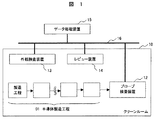
図1は、本発明の欠陥レビュー方法および装置の適用対象例である欠陥確認システムを示す全体構成図である。清浄な環境が保たれたクリーンルーム10内に、半導体製造工程11とプローブ検査装置12がある。例えば、ウエハ製品の外観不良の検出を行うために、外観検査装置13が設けられており、この外観検査装置13からのデータに基づき、欠陥(外観不良)の観察、すなわちレビューを行うレビュー装置14が設置されている。外観検査装置13とレビュー装置14は、検査・画像データを受け渡すためのデータ処理装置15に、通信回線16で結ばれている。製品となるウエハは、ロット単位で半導体製造工程11を流れている。外観検査装置13は、予め、外観検査を行うことが決められている工程の処理が終了した後に、作業者あるいは搬送機によって運ばれ、検査処理が行われる。
FIG. 1 is an overall configuration diagram showing a defect confirmation system as an application target example of the defect review method and apparatus of the present invention. In a
図2は、図1の欠陥確認システムにおける欠陥レビューまでの情報の流れの説明図である。外観検査を行った際の欠陥情報23は、ロット番号とウエハ番号と検査工程と検査日時を用いてデータ処理装置15で管理される。
FIG. 2 is an explanatory diagram of the flow of information up to the defect review in the defect confirmation system of FIG. The
ここで、一旦、図2の説明を中断し、図3および図4を先に説明する。 Here, the description of FIG. 2 is temporarily interrupted, and FIGS. 3 and 4 will be described first.
図3は、検査装置とレビュー装置間でやり取りされる欠陥情報23の一例図である。この欠陥情報23には、ロット番号31、ウエハID32、そのダイレイアウト33、検査中に検出した欠陥ID34とその座標情報など35で構成される。その他、欠陥情報23には、例えば、自動欠陥レビュー(ADR)画像、欠陥特徴量情報(実時間欠陥分類(RDC)情報)等がある。
FIG. 3 is an example of
図4は、欠陥検査装置から出力される実時間欠陥分類(RDC)における特徴パラメータ40の一例を示す画面図である。考えられる欠陥特徴量情報の例としては、図4および以下に述べるものが挙げられる。これらのデータは、その他の欠陥情報とともに、決められたフォーマットのテキストデータによって送信される。
FIG. 4 is a screen diagram illustrating an example of the
まず、(1)最大グレーレベル差は、欠陥として判定された場所の画像と、その参照部の画像を、画像処理して差画像を得た時の、欠陥部の明るさの絶対値である。(2)参照画像平均グレーレベルとは、その欠陥部と判定されたピクセル部の、参照画像上の明るさの平均値、(3)欠陥画像平均グレーレベルとは、その欠陥部と判定されたピクセル部の、欠陥画像上の明るさの平均値である。(4)極性とは、欠陥部が参照画像に比べ明るいか暗いかを示すものであり、「+」は明るい欠陥、「−」は暗い欠陥を示す。(5)検査モードとはその欠陥が検出されたときに使用されていた画像比較方式で、ダイ比較、セル比較、それらの混合比較などがある。(6)欠陥サイズや(7)欠陥画素数、(8)欠陥サイズ幅や(9)欠陥サイズ高さは、検出された欠陥の大きさを示すもので、欠陥サイズ、幅や高さの単位はミクロンなど、欠陥画素数の単位はピクセルである。(10)欠陥サイズ比は、欠陥サイズの幅/高さ比を表すもので、幅と高さが同じであれば1、幅が高さの2倍あれば2、などとあらわすパラメータである。最後に、(11)と(12)の欠陥部画素微分値とは、欠陥画像または参照画像上の欠陥とされたピクセル部の微分値を表したものであり、そのピクセル部内の濃淡の変化の度合いを示したものである。その欠陥画像部の値を(11)欠陥画像中欠陥部画素微分値、参照画像部のそれを(12)参照画像中欠陥部画素微分値と呼ぶ。 First, (1) the maximum gray level difference is an absolute value of the brightness of the defective part when the image of the place determined as the defect and the image of the reference part are subjected to image processing to obtain a difference image. . (2) The reference image average gray level is the average brightness on the reference image of the pixel portion determined to be the defective portion, and (3) the defect image average gray level is determined to be the defective portion. It is an average value of the brightness of the pixel portion on the defect image. (4) Polarity indicates whether the defect portion is brighter or darker than the reference image, where “+” indicates a bright defect and “−” indicates a dark defect. (5) The inspection mode is an image comparison method used when the defect is detected, and includes die comparison, cell comparison, and mixed comparison thereof. (6) Defect size, (7) Number of defective pixels, (8) Defect size width, and (9) Defect size height indicate the size of the detected defect and are units of defect size, width, and height. Is the unit of the number of defective pixels, such as a micron. (10) The defect size ratio represents the width / height ratio of the defect size, and is a parameter that represents 1 if the width and height are the same, and 2 if the width is twice the height. Finally, the defective pixel differential values of (11) and (12) represent the differential values of the defective pixel portion on the defective image or the reference image, and the change in shading in the pixel portion. It shows the degree. The value of the defective image portion is referred to as (11) the defective pixel differential value in the defect image, and that of the reference image portion is referred to as (12) the defective pixel differential value in the reference image.
ここで、図2に戻って、情報と処理の流れを説明する。外観検査を終了したウエハは、外観不良(欠陥)をレビューするためにレビュー装置21,22に運ばれ、ロット内から予め決められているウエハを取り出してレビューを行う。光学式レビュー装置21やSEM式レビュー装置22でレビューを行う際は、レビュー対象であるウエハの情報、すなわちロット番号とウエハ番号と検査工程をキー情報として、データ処理装置15から欠陥情報24,25を取得する。これらの情報24,25には、欠陥IDと座標データだけでなく、検査時に得られた自動欠陥レビュー(ADR)画像も含んでいる。
Here, returning to FIG. 2, the flow of information and processing will be described. The wafer having undergone the appearance inspection is carried to the
検査装置13が出力する欠陥情報23は膨大なデータであるため、複数のフィルター機能によりデータ処理装置15によって抽出された欠陥情報24,25のみが光学式レビュー装置21やSEM式レビュー装置22に通信回線16を通して送られる。欠陥情報24,25のフォーマットは、一般には欠陥情報23と同じである。
Since the
抽出された欠陥情報24,25に基づいて、光学式レビュー装置21またはSEM式レビュー装置22において欠陥検出部の画像が取得され、その画像を用いて各レビュー装置に搭載されている自動欠陥分類(ADC)機能で欠陥分類を行う。それらの情報は、自動欠陥レビュー(ADR)/自動欠陥分類(ADC)情報26,27として通信回線16を通してデータ処理装置15に送られる。
Based on the extracted
図5は、データ処理装置によってデータ突合せ処理した画面の一例図である。この図を用いて、検査装置から出力された検査・欠陥特徴量・画像データ、及びレビュー装置側から出力された自動欠陥レビュー(ADR)/自動欠陥分類(ADC)情報を、データ処理装置15でどのように処理/表示させるかについて説明する。
FIG. 5 is an example of a screen on which data matching processing is performed by the data processing apparatus. Using this figure, the
検査装置からの多量の検査/画像データ23、レビュー装置21,22からの多量の自動欠陥レビュー(ADR)/自動欠陥分類(ADC)情報を並べて表示するため、データ処理装置15上には、図5に示す画面50が用意されている。
A large amount of inspection /
画面50は、特許文献3の図4や図11とほぼ同じであり、異なる点は、基本画面への移行ボタン51を備えている点である。
The
次に、図6から図11を用いて、図5の画面50中に設けた本発明の一実施例に係る基本画面移行ボタン51の機能、画面構成について説明する。
Next, the function and screen configuration of the basic
図6は、基本画面選択ウィンドーであり、図7で後述する基本画面を選択するためのものである。 FIG. 6 is a basic screen selection window for selecting a basic screen described later in FIG.
図7に示す基本画面に表示させたい画像を、図6の基本画面選択ウィンドー60内のボックス61群のいずれかを選んでチェックマーク(レ印)をつけることで選択する事が出来る。その上で、OKボタン62を押すことによって、図7に示す基本画面に移る。
The image to be displayed on the basic screen shown in FIG. 7 can be selected by selecting any of the
図7は、本発明の一実施例による基本画面の画面表示例図である。基本画面700には、図5のウィンドー50で選択した欠陥の分布を示す欠陥マップ710と、欠陥画像一覧720が並んでいる。画像一覧720は、スクロールバー721により、画像一覧720の表示面を上下方向にスクロールする事が出来る。
FIG. 7 is a screen display example of a basic screen according to an embodiment of the present invention. On the
マップ710には、欠陥を示すドット711を表示するほかに、画像一覧720に表示している欠陥を、マップ710内に、大きなドット712により表示している。マップ上の任意のドット711,712をクリックすれば、その欠陥写真を画像一覧720に表示する。
In addition to displaying
一方、画像一覧720内の任意の欠陥画像をクリックすることで、対応する欠陥を、マップ710内の点滅するドットにより表示する。これらドットや画像の選択において、シフト(Shift)キーを押しながら実行すると、複数の欠陥を選択する事が可能である。
On the other hand, by clicking an arbitrary defect image in the
欠陥ID入力欄701により、任意の欠陥を選択すると、マップ710上に点滅するドットによりその欠陥の位置を示しながら、画像一覧720内には、該当欠陥の写真(画像)を明示する。
When an arbitrary defect is selected in the defect
また、画像一覧720内の画像をクリック選択し、分類入力(Class# Input)欄702に任意の分類(数字)を入力し、リターンキー(図示せず)を押すと、その欠陥に対する分類(Class)番号を入力する事が出来る。
When an image in the
マップオン窓703についているチェックマーク(レ印)をはずした場合、マップ710は画面から消え、図8に示すように、画面いっぱいに画像一覧720が表示される。
When the check mark (label) attached to the map-on
画像一覧720に表示させる欠陥数を絞込見たい場合には、データ絞込み(Data Filtering)ボタン704を押す。すると、図9に示すウィンドー90が現れる。
In order to narrow down the number of defects to be displayed in the
図9は、本発明の一実施例による基本画面に表示する欠陥画像絞込みウィンドーである。このウィンドー90により、予め入力している分類(Class)番号による選択欄91、または図5のウィンドー50に表示されている欠陥特徴量の範囲を選択する選択欄92に選択範囲を入力し、OKボタン93を押す。これにより、図7のウィンドー700の画像一覧720に表示させる欠陥数を絞込む事が出来る。なお、図9において、94は全選択ボタン、95は選択クリアボタン、96はウィンドークローズボタン、97はキャンセルボタンである。
FIG. 9 is a defect image narrowing window displayed on the basic screen according to an embodiment of the present invention. In this
さて、図7の基本画面に戻って説明を進める。 Now, returning to the basic screen of FIG.
画像を大きくして観察したい場合、手段として2種類用意している。 When it is desired to observe an enlarged image, two types of means are prepared.
まず、第1に、図7の拡大(Expand)ボタン705を押すことにより、図10に示す欠陥画像拡大表示画面100が現れる。
First, when the expand
図10は、本発明の一実施例による基本画面において欠陥画像を拡大表示する一例画面表示例図である。この画面100の左側にはマップ101が、図7と同様に表示されている。一方、右側には、下方に、図7と同じ大きさの欠陥画像が横一列に表示されながら、そのうちの選択画像一枚を中央部に拡大表示させた拡大画像102とともに、その拡大画像に対応する欠陥の情報103を表示している。また、マップ101内には、他の欠陥ドット104と共に、大きく点滅するドット105により当該欠陥の場所が明示される。
FIG. 10 is an example screen display example for enlarging and displaying a defect image on a basic screen according to an embodiment of the present invention. A
なお、106は図7の基本画面への戻すためのイメージギャラリー(Image Gallery)ボタン、107は、欠陥IDが1つ前の欠陥画像に移動するためのボタン、108は、欠陥IDが1つ後ろの欠陥画像に移動するためのボタン、109は、スクロールボタンである。
In addition, 106 is an image gallery button for returning to the basic screen of FIG. 7, 107 is a button for moving to the defect image with the previous defect ID, and 108 is behind the defect ID. A
第2に、図7、8、および10に示す任意の欠陥画像をクリックすると、図11に示すウィンドー110が現れ、検査装置の画像111及びレビュー装置の画像112を確認する事が出来る。ボタン113及び114により、前後の欠陥IDの画像を確認することも出来る。また、任意の分類(Class)番号を入力欄115から入力することも出来る。クローズボタン116を押すことで、このウィンドー110を閉じる事が出来る。
Second, when an arbitrary defect image shown in FIGS. 7, 8 and 10 is clicked, a
最後に、再び図7に戻って、戻り(Back)ボタン706を押すことにより、図5に示したウィンドー50に戻る事が出来る。
Finally, returning to FIG. 7 again, by pressing the
本実施例によれば、外観検査装置から出力されるデータをデータ処理装置15に取込み、画像データの表示と操作手段の工夫により、容易に大量の画像データをレビューする事が出来る欠陥レビュー装置を提供する事が出来る。
According to the present embodiment, a defect review apparatus that can take in data output from an appearance inspection apparatus into the
10…クリーンルーム、11…半導体製造工程、12…プローブ検査装置、13…外観検査装置、14…レビュー装置、15…データ処理装置、16…通信回線、21…光学式レビュー装置、22…SEM式レビュー装置、23…欠陥画像情報、24,25…欠陥座標情報、26,27…欠陥画像情報、50…データ処理装置画面、51…基本画面移行ボタン、60…基本画面画像選択ウィンドー、61…画像選択ボタン、62…OKボタン、700…基本画面、710…欠陥マップ、711…欠陥ドット、712…画像表示させている欠陥ドット、720…欠陥画像一覧、721…スクロールバー、701…任意の欠陥ID検索インプット欄、702…欠陥クラスコード入力欄、703…Map表示ONボタン、704…データフィルタリングボタン、705…画像拡大表示ボタン、706…Backボタン、90…表示欠陥フィルタリングウィンドー、91…表示クラス番号選択欄、92…表示欠陥特徴量範囲選択欄、93…OKボタン、94…全選択ボタン、95…選択クリアボタン、96…ウィンドークローズボタン、97…Cancelボタン、100…画像拡大表示ウィンドー、101…欠陥マップ、102…欠陥拡大画像表示部、103…画像拡大表示させている欠陥情報表示欄、104…欠陥ドット、105…画像拡大している欠陥の位置を示すドット、106…画像一覧表示に戻るボタン、107…欠陥IDが一つ前の画像に移動するためのボタン、108…欠陥IDが一つ後ろの画像に移動するためのボタン、109…スクロールボタン、110…画像拡大表示ウィンドー、111…欠陥ID表示欄、112…欠陥クラス番号入力欄、113…欠陥検査装置画像、114…レビュー装置画像、115…欠陥IDが一つ前の画像に移動するためのボタン、116…欠陥IDが一つ後ろの画像に移動するためのボタン。
DESCRIPTION OF
Claims (19)
前記外観検査装置によって取得された画像および前記レビュー装置によって取得された画像を含む複数種類の画像の中から、前記被検体の検査領域における欠陥の存在を明示する欠陥マップおよび前記欠陥マップ内の多数の欠陥に対応して用意された欠陥画像表示面を並べた欠陥画像一覧に表示させる画像の種類を指定する操作入力信号を受付けたとき、前記指定に応じた種類の画像を選択する表示種類画像選択ステップ、
前記表示種類画像選択ステップによって選択された種類の欠陥画像について、前記欠陥マップと前記欠陥画像一覧とを、画面上に並べて表示するステップ、
前記欠陥マップ上の任意の欠陥を指定する操作入力信号を受付けたとき、前記欠陥画像一覧中における、指定された欠陥に対応する表示面を、他の欠陥画像の表示画面と区別して表示する画像区別表示ステップ、および
前記欠陥画像一覧中の任意の欠陥を指定する操作入力信号を受付けたとき、前記欠陥マップ上における指定された欠陥に対応する欠陥を、他の欠陥と区別して表示するマップ欠陥の区別表示ステップを備えたことを特徴とする欠陥レビュー方法。 In a defect review method using a review device that reviews defects of the subject based on information obtained by an appearance inspection device that inspects the appearance of the subject.
Among a plurality of types of images including an image acquired by the appearance inspection apparatus and an image acquired by the review apparatus , a defect map that clearly indicates the presence of a defect in the inspection region of the subject and a large number in the defect map Display type image for selecting the type of image corresponding to the designation when receiving an operation input signal for designating the type of image to be displayed in the defect image list in which the defect image display surfaces prepared corresponding to the defect are arranged Selection step,
The display type image about the type of defect image selected by the selecting step, the step of displaying said defect map and said defect image list, side by side on the screen,
When accepting an operation input signal specifying an arbitrary defects on the defect map, the image in the defect image in the list, the display surface corresponding to the specified defect is displayed differently from the display screen of another defect image A map defect for displaying a defect corresponding to the designated defect on the defect map in distinction from other defects when receiving an operation input signal for designating an arbitrary defect in the defect image list; A defect review method characterized by comprising a distinction display step.
前記外観検査装置によって取得された画像および前記レビュー装置によって取得された画像を含む複数種類の画像の中から、前記被検体の検査領域における欠陥の存在を明示する欠陥マップおよび前記欠陥マップ内の多数の欠陥に対応して用意された欠陥画像表示面を並べた欠陥画像一覧に表示させる画像の種類を指定する操作入力信号を受付けたとき、前記指定に応じた種類の画像を選択する表示種類画像選択手段と、
前記表示種類画像選択手段によって選択された画像の欠陥について、前記欠陥マップと前記欠陥画像一覧とを、画面上に並べて表示する表示手段と、
前記欠陥マップ上の任意の欠陥を指定するための操作入力手段と、
前記欠陥画像一覧中における任意の欠陥画像を指定するための操作入力手段と、
前記欠陥マップ上の任意の欠陥が指定されたとき、前記欠陥画像一覧中における、指定された欠陥に対応する欠陥の画像を、他の欠陥画像の表示画面と区別して表示する画像区別表示手段と、
前記欠陥画像一覧中の任意の欠陥が指定されたとき、前記欠陥マップ上における、指定された欠陥に対応する欠陥を、他の欠陥と区別して表示するマップ欠陥の区別表示手段を備えたことを特徴とする欠陥レビュー装置。 In a defect review apparatus that reviews defects of the subject based on information obtained by an appearance inspection device that inspects the appearance of the subject.
Among a plurality of types of images including an image acquired by the appearance inspection apparatus and an image acquired by the review apparatus , a defect map that clearly indicates the presence of a defect in the inspection region of the subject and a large number in the defect map Display type image for selecting the type of image corresponding to the designation when receiving an operation input signal for designating the type of image to be displayed in the defect image list in which the defect image display surfaces prepared corresponding to the defect are arranged A selection means;
The defect image selected by the display type image selecting means and the defect image list and the defect map, and display means for displaying side by side on the screen,
Operation input means for designating an arbitrary defect on the defect map;
Operation input means for designating an arbitrary defect image in the defect image list;
When any defect on the defect map is designated, in the defect image in the list, the image of the defect corresponding to the specified defect, an image distinguishing display means for displaying as distinguished from the display screen of another defect image ,
When an arbitrary defect in the defect image list is designated, map defect distinction display means for displaying the defect corresponding to the designated defect on the defect map separately from other defects is provided. Feature defect review equipment.
Priority Applications (3)
| Application Number | Priority Date | Filing Date | Title |
|---|---|---|---|
| JP2006316903A JP4976112B2 (en) | 2006-11-24 | 2006-11-24 | Defect review method and apparatus |
| TW096141497A TWI369751B (en) | 2006-11-24 | 2007-11-02 | A method of reviewing defects and an apparatus thereon |
| US11/984,721 US20080123936A1 (en) | 2006-11-24 | 2007-11-21 | Method of reviewing defects and an apparatus thereon |
Applications Claiming Priority (1)
| Application Number | Priority Date | Filing Date | Title |
|---|---|---|---|
| JP2006316903A JP4976112B2 (en) | 2006-11-24 | 2006-11-24 | Defect review method and apparatus |
Publications (2)
| Publication Number | Publication Date |
|---|---|
| JP2008130966A JP2008130966A (en) | 2008-06-05 |
| JP4976112B2 true JP4976112B2 (en) | 2012-07-18 |
Family
ID=39463764
Family Applications (1)
| Application Number | Title | Priority Date | Filing Date |
|---|---|---|---|
| JP2006316903A Active JP4976112B2 (en) | 2006-11-24 | 2006-11-24 | Defect review method and apparatus |
Country Status (3)
| Country | Link |
|---|---|
| US (1) | US20080123936A1 (en) |
| JP (1) | JP4976112B2 (en) |
| TW (1) | TWI369751B (en) |
Families Citing this family (8)
| Publication number | Priority date | Publication date | Assignee | Title |
|---|---|---|---|---|
| JP2009272497A (en) * | 2008-05-08 | 2009-11-19 | Hitachi High-Technologies Corp | Recipe parameter management apparatus and recipe parameter management method |
| JP2009270976A (en) * | 2008-05-08 | 2009-11-19 | Hitachi High-Technologies Corp | Flaw reviewing method and flaw reviewing apparatus |
| JP2011061047A (en) * | 2009-09-11 | 2011-03-24 | Hitachi High-Technologies Corp | Defect review support device, defect review device, and inspection support device |
| TW201310561A (en) * | 2011-08-30 | 2013-03-01 | Rexchip Electronics Corp | Wafer defect analysis and trouble-shooting method of defect cause |
| JP5707291B2 (en) | 2011-09-29 | 2015-04-30 | 株式会社日立ハイテクノロジーズ | Charged particle beam system that supports image classification |
| FR2980870B1 (en) * | 2011-10-03 | 2013-09-20 | Accelonix | IMAGING ARRANGEMENT FOR INSPECTING ELECTRONIC CARDS, SYSTEM THEREFOR |
| JP6815251B2 (en) * | 2017-03-30 | 2021-01-20 | 東京エレクトロン株式会社 | Inspection system, wafer map display, wafer map display method, and computer program |
| CN113310997A (en) * | 2021-07-30 | 2021-08-27 | 苏州维嘉科技股份有限公司 | PCB defect confirmation method and device, automatic optical detection equipment and storage medium |
Family Cites Families (9)
| Publication number | Priority date | Publication date | Assignee | Title |
|---|---|---|---|---|
| US6259960B1 (en) * | 1996-11-01 | 2001-07-10 | Joel Ltd. | Part-inspecting system |
| JP4583680B2 (en) * | 2001-09-28 | 2010-11-17 | パナソニック株式会社 | Solid-state imaging device |
| US6959251B2 (en) * | 2002-08-23 | 2005-10-25 | Kla-Tencor Technologies, Corporation | Inspection system setup techniques |
| JP2004177139A (en) * | 2002-11-25 | 2004-06-24 | Renesas Technology Corp | Support program for preparation of inspection condition data, inspection device, and method of preparing inspection condition data |
| US8532949B2 (en) * | 2004-10-12 | 2013-09-10 | Kla-Tencor Technologies Corp. | Computer-implemented methods and systems for classifying defects on a specimen |
| US7606409B2 (en) * | 2004-11-19 | 2009-10-20 | Hitachi High-Technologies Corporation | Data processing equipment, inspection assistance system, and data processing method |
| JP4413767B2 (en) * | 2004-12-17 | 2010-02-10 | 株式会社日立ハイテクノロジーズ | Pattern inspection device |
| JP2006310551A (en) * | 2005-04-28 | 2006-11-09 | Hitachi High-Technologies Corp | Inspection support system and method |
| JP4699873B2 (en) * | 2005-11-10 | 2011-06-15 | 株式会社日立ハイテクノロジーズ | Defect data processing and review equipment |
-
2006
- 2006-11-24 JP JP2006316903A patent/JP4976112B2/en active Active
-
2007
- 2007-11-02 TW TW096141497A patent/TWI369751B/en active
- 2007-11-21 US US11/984,721 patent/US20080123936A1/en not_active Abandoned
Also Published As
| Publication number | Publication date |
|---|---|
| US20080123936A1 (en) | 2008-05-29 |
| TW200834776A (en) | 2008-08-16 |
| TWI369751B (en) | 2012-08-01 |
| JP2008130966A (en) | 2008-06-05 |
Similar Documents
| Publication | Publication Date | Title |
|---|---|---|
| JP4699873B2 (en) | Defect data processing and review equipment | |
| US6973209B2 (en) | Defect inspection system | |
| JP2004294358A (en) | Defect inspection method and apparatus | |
| US8041443B2 (en) | Surface defect data display and management system and a method of displaying and managing a surface defect data | |
| JP4774383B2 (en) | Data processing apparatus and data processing method | |
| US20080123936A1 (en) | Method of reviewing defects and an apparatus thereon | |
| US20160210526A1 (en) | Visual Feedback for Inspection Algorithms and Filters | |
| JP4597155B2 (en) | Data processing apparatus and data processing method | |
| JP6049052B2 (en) | Wafer visual inspection apparatus and sensitivity threshold setting method in wafer visual inspection apparatus | |
| JP2002277412A (en) | Inspection screen displaying method and substrate inspection system | |
| JP4374381B2 (en) | Inspection support system, data processing apparatus, and data processing method | |
| US20060111879A1 (en) | Data processing equipment, inspection assistance system, and data processing method | |
| JP4652917B2 (en) | DEFECT DATA PROCESSING METHOD AND DATA PROCESSING DEVICE | |
| JP4741936B2 (en) | Data processing apparatus, inspection work support system, and data processing method | |
| JP2001305075A (en) | Appearance inspection device | |
| JP2009168476A (en) | Defect inspection method and defect inspection system | |
| JP2000097871A (en) | Review equipment | |
| JP2018091771A (en) | Method for inspection, preliminary image selection device, and inspection system | |
| JP4857155B2 (en) | Data processing apparatus, inspection system, and data processing method | |
| JP5039594B2 (en) | Review device, inspection area setting support system, and defect image acquisition method | |
| JP5291419B2 (en) | Data processing apparatus, data processing method, and inspection work support system using the same | |
| JP4943777B2 (en) | DEFECT DATA PROCESSING DEVICE, DEFECT DATA PROCESSING SYSTEM, AND DEFECT DATA PROCESSING METHOD |
Legal Events
| Date | Code | Title | Description |
|---|---|---|---|
| A621 | Written request for application examination |
Free format text: JAPANESE INTERMEDIATE CODE: A621 Effective date: 20081212 |
|
| A977 | Report on retrieval |
Free format text: JAPANESE INTERMEDIATE CODE: A971007 Effective date: 20111028 |
|
| A131 | Notification of reasons for refusal |
Free format text: JAPANESE INTERMEDIATE CODE: A131 Effective date: 20111115 |
|
| A521 | Request for written amendment filed |
Free format text: JAPANESE INTERMEDIATE CODE: A523 Effective date: 20120113 |
|
| TRDD | Decision of grant or rejection written | ||
| A01 | Written decision to grant a patent or to grant a registration (utility model) |
Free format text: JAPANESE INTERMEDIATE CODE: A01 Effective date: 20120410 |
|
| A01 | Written decision to grant a patent or to grant a registration (utility model) |
Free format text: JAPANESE INTERMEDIATE CODE: A01 |
|
| A61 | First payment of annual fees (during grant procedure) |
Free format text: JAPANESE INTERMEDIATE CODE: A61 Effective date: 20120412 |
|
| R150 | Certificate of patent or registration of utility model |
Ref document number: 4976112 Country of ref document: JP Free format text: JAPANESE INTERMEDIATE CODE: R150 Free format text: JAPANESE INTERMEDIATE CODE: R150 |
|
| FPAY | Renewal fee payment (event date is renewal date of database) |
Free format text: PAYMENT UNTIL: 20150420 Year of fee payment: 3 |
|
| S531 | Written request for registration of change of domicile |
Free format text: JAPANESE INTERMEDIATE CODE: R313531 |
|
| S533 | Written request for registration of change of name |
Free format text: JAPANESE INTERMEDIATE CODE: R313533 |
|
| R350 | Written notification of registration of transfer |
Free format text: JAPANESE INTERMEDIATE CODE: R350 |