JP4974492B2 - Light emitting device - Google Patents
Light emitting device Download PDFInfo
- Publication number
- JP4974492B2 JP4974492B2 JP2005234205A JP2005234205A JP4974492B2 JP 4974492 B2 JP4974492 B2 JP 4974492B2 JP 2005234205 A JP2005234205 A JP 2005234205A JP 2005234205 A JP2005234205 A JP 2005234205A JP 4974492 B2 JP4974492 B2 JP 4974492B2
- Authority
- JP
- Japan
- Prior art keywords
- transistor
- light emitting
- emitting element
- potential
- monitor
- Prior art date
- Legal status (The legal status is an assumption and is not a legal conclusion. Google has not performed a legal analysis and makes no representation as to the accuracy of the status listed.)
- Active
Links
- 230000002441 reversible effect Effects 0.000 claims description 26
- 238000012544 monitoring process Methods 0.000 description 45
- 230000008859 change Effects 0.000 description 34
- 230000006866 deterioration Effects 0.000 description 19
- 238000000034 method Methods 0.000 description 16
- 230000007613 environmental effect Effects 0.000 description 15
- 239000000758 substrate Substances 0.000 description 15
- 239000010410 layer Substances 0.000 description 13
- 239000000463 material Substances 0.000 description 12
- 239000004065 semiconductor Substances 0.000 description 12
- 239000003990 capacitor Substances 0.000 description 11
- IJGRMHOSHXDMSA-UHFFFAOYSA-N Atomic nitrogen Chemical compound N#N IJGRMHOSHXDMSA-UHFFFAOYSA-N 0.000 description 8
- 239000000956 alloy Substances 0.000 description 8
- 239000011368 organic material Substances 0.000 description 8
- 239000010936 titanium Substances 0.000 description 8
- XUIMIQQOPSSXEZ-UHFFFAOYSA-N Silicon Chemical compound [Si] XUIMIQQOPSSXEZ-UHFFFAOYSA-N 0.000 description 7
- 230000007547 defect Effects 0.000 description 7
- 229910052751 metal Inorganic materials 0.000 description 7
- 239000002184 metal Substances 0.000 description 7
- 229910052710 silicon Inorganic materials 0.000 description 7
- 239000010703 silicon Substances 0.000 description 7
- VYPSYNLAJGMNEJ-UHFFFAOYSA-N silicon dioxide Inorganic materials O=[Si]=O VYPSYNLAJGMNEJ-UHFFFAOYSA-N 0.000 description 7
- 229910052814 silicon oxide Inorganic materials 0.000 description 7
- 229910052581 Si3N4 Inorganic materials 0.000 description 6
- 229910045601 alloy Inorganic materials 0.000 description 6
- 239000012535 impurity Substances 0.000 description 6
- 239000011229 interlayer Substances 0.000 description 6
- 230000002829 reductive effect Effects 0.000 description 6
- HQVNEWCFYHHQES-UHFFFAOYSA-N silicon nitride Chemical compound N12[Si]34N5[Si]62N3[Si]51N64 HQVNEWCFYHHQES-UHFFFAOYSA-N 0.000 description 6
- 229910052782 aluminium Inorganic materials 0.000 description 5
- 150000001875 compounds Chemical class 0.000 description 5
- 230000001747 exhibiting effect Effects 0.000 description 5
- 229910010272 inorganic material Inorganic materials 0.000 description 5
- 239000011147 inorganic material Substances 0.000 description 5
- 238000004519 manufacturing process Methods 0.000 description 5
- 239000011159 matrix material Substances 0.000 description 5
- 229910052719 titanium Inorganic materials 0.000 description 5
- 229910052721 tungsten Inorganic materials 0.000 description 5
- RTAQQCXQSZGOHL-UHFFFAOYSA-N Titanium Chemical compound [Ti] RTAQQCXQSZGOHL-UHFFFAOYSA-N 0.000 description 4
- 239000010949 copper Substances 0.000 description 4
- 230000008878 coupling Effects 0.000 description 4
- 238000010168 coupling process Methods 0.000 description 4
- 238000005859 coupling reaction Methods 0.000 description 4
- 229910052750 molybdenum Inorganic materials 0.000 description 4
- 229910052757 nitrogen Inorganic materials 0.000 description 4
- -1 polyethylene terephthalate Polymers 0.000 description 4
- WFKWXMTUELFFGS-UHFFFAOYSA-N tungsten Chemical compound [W] WFKWXMTUELFFGS-UHFFFAOYSA-N 0.000 description 4
- 239000010937 tungsten Substances 0.000 description 4
- ZOKXTWBITQBERF-UHFFFAOYSA-N Molybdenum Chemical compound [Mo] ZOKXTWBITQBERF-UHFFFAOYSA-N 0.000 description 3
- PXHVJJICTQNCMI-UHFFFAOYSA-N Nickel Chemical compound [Ni] PXHVJJICTQNCMI-UHFFFAOYSA-N 0.000 description 3
- KDLHZDBZIXYQEI-UHFFFAOYSA-N Palladium Chemical compound [Pd] KDLHZDBZIXYQEI-UHFFFAOYSA-N 0.000 description 3
- ATJFFYVFTNAWJD-UHFFFAOYSA-N Tin Chemical compound [Sn] ATJFFYVFTNAWJD-UHFFFAOYSA-N 0.000 description 3
- XAGFODPZIPBFFR-UHFFFAOYSA-N aluminium Chemical compound [Al] XAGFODPZIPBFFR-UHFFFAOYSA-N 0.000 description 3
- QVGXLLKOCUKJST-UHFFFAOYSA-N atomic oxygen Chemical compound [O] QVGXLLKOCUKJST-UHFFFAOYSA-N 0.000 description 3
- 239000002585 base Substances 0.000 description 3
- 229910052802 copper Inorganic materials 0.000 description 3
- 230000002950 deficient Effects 0.000 description 3
- KPUWHANPEXNPJT-UHFFFAOYSA-N disiloxane Chemical class [SiH3]O[SiH3] KPUWHANPEXNPJT-UHFFFAOYSA-N 0.000 description 3
- PCHJSUWPFVWCPO-UHFFFAOYSA-N gold Chemical compound [Au] PCHJSUWPFVWCPO-UHFFFAOYSA-N 0.000 description 3
- 238000010438 heat treatment Methods 0.000 description 3
- 239000011733 molybdenum Substances 0.000 description 3
- 239000001301 oxygen Substances 0.000 description 3
- 229910052760 oxygen Inorganic materials 0.000 description 3
- BASFCYQUMIYNBI-UHFFFAOYSA-N platinum Chemical compound [Pt] BASFCYQUMIYNBI-UHFFFAOYSA-N 0.000 description 3
- 229920001709 polysilazane Polymers 0.000 description 3
- 229920006395 saturated elastomer Polymers 0.000 description 3
- 125000001424 substituent group Chemical group 0.000 description 3
- RYGMFSIKBFXOCR-UHFFFAOYSA-N Copper Chemical compound [Cu] RYGMFSIKBFXOCR-UHFFFAOYSA-N 0.000 description 2
- UFHFLCQGNIYNRP-UHFFFAOYSA-N Hydrogen Chemical compound [H][H] UFHFLCQGNIYNRP-UHFFFAOYSA-N 0.000 description 2
- 239000004695 Polyether sulfone Substances 0.000 description 2
- 239000004642 Polyimide Substances 0.000 description 2
- 239000004372 Polyvinyl alcohol Substances 0.000 description 2
- XLOMVQKBTHCTTD-UHFFFAOYSA-N Zinc monoxide Chemical compound [Zn]=O XLOMVQKBTHCTTD-UHFFFAOYSA-N 0.000 description 2
- NIXOWILDQLNWCW-UHFFFAOYSA-N acrylic acid group Chemical group C(C=C)(=O)O NIXOWILDQLNWCW-UHFFFAOYSA-N 0.000 description 2
- 239000010405 anode material Substances 0.000 description 2
- 238000013459 approach Methods 0.000 description 2
- 125000004429 atom Chemical group 0.000 description 2
- 239000010406 cathode material Substances 0.000 description 2
- 230000001413 cellular effect Effects 0.000 description 2
- 239000011651 chromium Substances 0.000 description 2
- 238000002425 crystallisation Methods 0.000 description 2
- 230000008025 crystallization Effects 0.000 description 2
- 238000005520 cutting process Methods 0.000 description 2
- 230000007423 decrease Effects 0.000 description 2
- 238000007599 discharging Methods 0.000 description 2
- 239000000428 dust Substances 0.000 description 2
- 238000005401 electroluminescence Methods 0.000 description 2
- 125000001153 fluoro group Chemical group F* 0.000 description 2
- 230000007274 generation of a signal involved in cell-cell signaling Effects 0.000 description 2
- 239000010931 gold Substances 0.000 description 2
- 239000001257 hydrogen Substances 0.000 description 2
- 229910052739 hydrogen Inorganic materials 0.000 description 2
- 229910052738 indium Inorganic materials 0.000 description 2
- APFVFJFRJDLVQX-UHFFFAOYSA-N indium atom Chemical compound [In] APFVFJFRJDLVQX-UHFFFAOYSA-N 0.000 description 2
- 229910003437 indium oxide Inorganic materials 0.000 description 2
- PJXISJQVUVHSOJ-UHFFFAOYSA-N indium(iii) oxide Chemical compound [O-2].[O-2].[O-2].[In+3].[In+3] PJXISJQVUVHSOJ-UHFFFAOYSA-N 0.000 description 2
- 238000002347 injection Methods 0.000 description 2
- 239000007924 injection Substances 0.000 description 2
- 150000002739 metals Chemical class 0.000 description 2
- 239000000203 mixture Substances 0.000 description 2
- 125000000962 organic group Chemical group 0.000 description 2
- 229920003207 poly(ethylene-2,6-naphthalate) Polymers 0.000 description 2
- 229920006393 polyether sulfone Polymers 0.000 description 2
- 239000011112 polyethylene naphthalate Substances 0.000 description 2
- 229920000139 polyethylene terephthalate Polymers 0.000 description 2
- 239000005020 polyethylene terephthalate Substances 0.000 description 2
- 229920001721 polyimide Polymers 0.000 description 2
- 229920002451 polyvinyl alcohol Polymers 0.000 description 2
- 230000008569 process Effects 0.000 description 2
- 230000000750 progressive effect Effects 0.000 description 2
- 230000001681 protective effect Effects 0.000 description 2
- 238000005070 sampling Methods 0.000 description 2
- 229910052709 silver Inorganic materials 0.000 description 2
- 239000002356 single layer Substances 0.000 description 2
- 229910052715 tantalum Inorganic materials 0.000 description 2
- 229910018125 Al-Si Inorganic materials 0.000 description 1
- 229910018520 Al—Si Inorganic materials 0.000 description 1
- 229910004261 CaF 2 Inorganic materials 0.000 description 1
- VYZAMTAEIAYCRO-UHFFFAOYSA-N Chromium Chemical compound [Cr] VYZAMTAEIAYCRO-UHFFFAOYSA-N 0.000 description 1
- XEEYBQQBJWHFJM-UHFFFAOYSA-N Iron Chemical compound [Fe] XEEYBQQBJWHFJM-UHFFFAOYSA-N 0.000 description 1
- 239000004952 Polyamide Substances 0.000 description 1
- 229910000577 Silicon-germanium Inorganic materials 0.000 description 1
- BQCADISMDOOEFD-UHFFFAOYSA-N Silver Chemical compound [Ag] BQCADISMDOOEFD-UHFFFAOYSA-N 0.000 description 1
- 229910002808 Si–O–Si Inorganic materials 0.000 description 1
- NRTOMJZYCJJWKI-UHFFFAOYSA-N Titanium nitride Chemical compound [Ti]#N NRTOMJZYCJJWKI-UHFFFAOYSA-N 0.000 description 1
- LEVVHYCKPQWKOP-UHFFFAOYSA-N [Si].[Ge] Chemical compound [Si].[Ge] LEVVHYCKPQWKOP-UHFFFAOYSA-N 0.000 description 1
- 239000003513 alkali Substances 0.000 description 1
- 229910052783 alkali metal Inorganic materials 0.000 description 1
- 150000001340 alkali metals Chemical class 0.000 description 1
- 229910052784 alkaline earth metal Inorganic materials 0.000 description 1
- 150000001342 alkaline earth metals Chemical class 0.000 description 1
- 125000000217 alkyl group Chemical group 0.000 description 1
- 239000005407 aluminoborosilicate glass Substances 0.000 description 1
- 150000001408 amides Chemical class 0.000 description 1
- 238000000137 annealing Methods 0.000 description 1
- 150000004945 aromatic hydrocarbons Chemical class 0.000 description 1
- 229910052788 barium Inorganic materials 0.000 description 1
- DSAJWYNOEDNPEQ-UHFFFAOYSA-N barium atom Chemical compound [Ba] DSAJWYNOEDNPEQ-UHFFFAOYSA-N 0.000 description 1
- 230000008901 benefit Effects 0.000 description 1
- UMIVXZPTRXBADB-UHFFFAOYSA-N benzocyclobutene Chemical compound C1=CC=C2CCC2=C1 UMIVXZPTRXBADB-UHFFFAOYSA-N 0.000 description 1
- 230000015572 biosynthetic process Effects 0.000 description 1
- 239000005388 borosilicate glass Substances 0.000 description 1
- 229910052792 caesium Inorganic materials 0.000 description 1
- 229910052791 calcium Inorganic materials 0.000 description 1
- 229910052804 chromium Inorganic materials 0.000 description 1
- 229910017052 cobalt Inorganic materials 0.000 description 1
- 239000010941 cobalt Substances 0.000 description 1
- GUTLYIVDDKVIGB-UHFFFAOYSA-N cobalt atom Chemical compound [Co] GUTLYIVDDKVIGB-UHFFFAOYSA-N 0.000 description 1
- 239000003086 colorant Substances 0.000 description 1
- 230000006378 damage Effects 0.000 description 1
- 238000001514 detection method Methods 0.000 description 1
- 238000011161 development Methods 0.000 description 1
- 230000005611 electricity Effects 0.000 description 1
- 238000001704 evaporation Methods 0.000 description 1
- 239000011521 glass Substances 0.000 description 1
- 229910052737 gold Inorganic materials 0.000 description 1
- 230000005525 hole transport Effects 0.000 description 1
- AMGQUBHHOARCQH-UHFFFAOYSA-N indium;oxotin Chemical compound [In].[Sn]=O AMGQUBHHOARCQH-UHFFFAOYSA-N 0.000 description 1
- 238000009413 insulation Methods 0.000 description 1
- 150000002500 ions Chemical class 0.000 description 1
- 238000003475 lamination Methods 0.000 description 1
- 239000011344 liquid material Substances 0.000 description 1
- 229910052744 lithium Inorganic materials 0.000 description 1
- 229910052749 magnesium Inorganic materials 0.000 description 1
- 239000007769 metal material Substances 0.000 description 1
- 229910052759 nickel Inorganic materials 0.000 description 1
- 150000004767 nitrides Chemical class 0.000 description 1
- 230000003647 oxidation Effects 0.000 description 1
- 238000007254 oxidation reaction Methods 0.000 description 1
- 229910052763 palladium Inorganic materials 0.000 description 1
- 230000003071 parasitic effect Effects 0.000 description 1
- 230000000737 periodic effect Effects 0.000 description 1
- 238000005268 plasma chemical vapour deposition Methods 0.000 description 1
- 239000004033 plastic Substances 0.000 description 1
- 229920003023 plastic Polymers 0.000 description 1
- 229910052697 platinum Inorganic materials 0.000 description 1
- 229920002647 polyamide Polymers 0.000 description 1
- 229920001690 polydopamine Polymers 0.000 description 1
- 239000002861 polymer material Substances 0.000 description 1
- 238000012545 processing Methods 0.000 description 1
- 239000010453 quartz Substances 0.000 description 1
- 229910052761 rare earth metal Inorganic materials 0.000 description 1
- 150000002910 rare earth metals Chemical class 0.000 description 1
- 230000003252 repetitive effect Effects 0.000 description 1
- 229920005989 resin Polymers 0.000 description 1
- 239000011347 resin Substances 0.000 description 1
- 239000004332 silver Substances 0.000 description 1
- 238000004544 sputter deposition Methods 0.000 description 1
- 239000010935 stainless steel Substances 0.000 description 1
- 229910001220 stainless steel Inorganic materials 0.000 description 1
- 239000007858 starting material Substances 0.000 description 1
- 230000003068 static effect Effects 0.000 description 1
- 229910052712 strontium Inorganic materials 0.000 description 1
- 229920003002 synthetic resin Polymers 0.000 description 1
- 239000000057 synthetic resin Substances 0.000 description 1
- GUVRBAGPIYLISA-UHFFFAOYSA-N tantalum atom Chemical compound [Ta] GUVRBAGPIYLISA-UHFFFAOYSA-N 0.000 description 1
- MZLGASXMSKOWSE-UHFFFAOYSA-N tantalum nitride Chemical compound [Ta]#N MZLGASXMSKOWSE-UHFFFAOYSA-N 0.000 description 1
- 230000036962 time dependent Effects 0.000 description 1
- 229910052723 transition metal Inorganic materials 0.000 description 1
- 150000003624 transition metals Chemical class 0.000 description 1
- 238000007740 vapor deposition Methods 0.000 description 1
- YVTHLONGBIQYBO-UHFFFAOYSA-N zinc indium(3+) oxygen(2-) Chemical compound [O--].[Zn++].[In+3] YVTHLONGBIQYBO-UHFFFAOYSA-N 0.000 description 1
Images


Description
本発明は、自発光素子を有する発光装置、及びその駆動方法に関する。 The present invention relates to a light emitting device having a self light emitting element and a driving method thereof.
近年、EL(Electro Luminescence)素子を代表とする発光素子を含む発光装置の開発が進められ、自発光型ゆえの高画質、広視野角、薄型、軽量等の利点を活かして、幅広い利用が期待されている。 In recent years, the development of light-emitting devices including light-emitting elements typified by EL (Electro Luminescence) elements has been promoted, and a wide range of uses is expected by taking advantage of self-luminous type such as high image quality, wide viewing angle, thinness, and light weight. Has been.
このような発光素子は経時劣化や初期不良を生じることがある。経時劣化や初期不良を防止するため、発光素子を作製するときに、陽極表面をPVA(ポリビニルアルコール)系の多孔質体などを用いて拭い、平坦化およびゴミの除去を行う方法が提案されている(特許文献1参照)。
本発明は、上記発光素子の経時劣化や初期不良に対し、上記特許文献1とは異なる新たな方法により解決することを課題とする。 An object of the present invention is to solve the deterioration with time and initial failure of the light-emitting element by a new method different from that of Patent Document 1.
上記課題を鑑み本発明は、発光装置の一部にモニター用発光素子を設け、該モニター素子の変動を考慮し、発光素子へ供給する電圧、又は電流を補正することを特徴とする。 In view of the above problems, the present invention is characterized in that a monitoring light emitting element is provided in a part of the light emitting device, and a voltage or a current supplied to the light emitting element is corrected in consideration of a variation of the monitoring element.
具体的な本発明の一形態は、複数のモニター用発光素子と、複数のモニター用発光素子が有する電極の電位の変化をモニターするモニター線と、複数のモニター用発光素子のいずれかがショートすると、モニター線を介してショートしたモニター用発光素子へ供給される電流を電気的に遮断する手段とを有する発光装置である。 A specific embodiment of the present invention is that when a plurality of monitor light emitting elements, a monitor line for monitoring a change in potential of an electrode included in the plurality of monitor light emitting elements, and any of the plurality of monitor light emitting elements are short-circuited, And a means for electrically interrupting the current supplied to the monitor light emitting element short-circuited through the monitor line.
また本発明の別形態は、モニター用発光素子と、モニター用発光素子に、一方の電極が接続されたモニター制御用トランジスタと、モニター制御用トランジスタのゲート電極に出力端子が接続され、かつモニター制御用トランジスタの一方の電極及びモニター用発光素子に入力端子が接続されたインバーターを有する発光装置である。 In another embodiment of the present invention, a monitor light emitting element, a monitor control transistor having one electrode connected to the monitor light emitting element, an output terminal connected to the gate electrode of the monitor control transistor, and monitor control The light emitting device includes an inverter having an input terminal connected to one electrode of the transistor for transistor and the light emitting element for monitor.
また本発明の別形態は、モニター用発光素子と、モニター用発光素子に接続されたモニター制御用トランジスタとを有し、モニター制御用トランジスタを、モニター用発光素子がショートしたときオフとする発光装置の駆動方法である。 Another embodiment of the present invention includes a light emitting device having a monitor light emitting element and a monitor control transistor connected to the monitor light emitting element, wherein the monitor control transistor is turned off when the monitor light emitting element is short-circuited. This is a driving method.
上記のように駆動させるため、インバーターは、モニター制御用トランジスタを、モニター用発光素子がショートしたときにオフさせる機能を有する回路である。そのため、本発明は該機能を有する回路であればインバーターに限定されるものではない。 In order to drive as described above, the inverter is a circuit having a function of turning off the monitor control transistor when the monitor light emitting element is short-circuited. Therefore, the present invention is not limited to an inverter as long as the circuit has the function.
またモニター用発光素子は、画素部に設けられた複数の発光素子と、同一工程により作製される。そのため、発光装置が置かれる環境の温度(単に、環境温度と表記する)や、経時変化(一般的には劣化することが多いため、経時劣化と表記する)に対する特性は、同じ、又はほぼ同じである。 The monitor light-emitting element is manufactured in the same process as the plurality of light-emitting elements provided in the pixel portion. Therefore, the characteristics with respect to the temperature of the environment in which the light emitting device is placed (simply referred to as environmental temperature) and the change with time (generally indicated as deterioration with time) are the same or almost the same. It is.
本発明により、環境温度の変化や経時劣化による輝度バラツキが低減された発光装置を提供することができる。 According to the present invention, it is possible to provide a light-emitting device in which luminance variations due to changes in environmental temperature and deterioration with time are reduced.
以下に、本発明の実施の形態を図面に基づいて説明する。但し、本発明は多くの異なる態様で実施することが可能であり、本発明の趣旨及びその範囲から逸脱することなくその形態及び詳細を様々に変更し得ることは当業者であれば容易に理解される。従って、本実施の形態の記載内容に限定して解釈されるものではない。なお、実施の形態を説明するための全図において、同一部分又は同様な機能を有する部分には同一の符号を付し、その繰り返しの説明は省略する。 Embodiments of the present invention will be described below with reference to the drawings. However, the present invention can be implemented in many different modes, and those skilled in the art can easily understand that the modes and details can be variously changed without departing from the spirit and scope of the present invention. Is done. Therefore, the present invention is not construed as being limited to the description of this embodiment mode. Note that in all the drawings for describing the embodiments, the same portions or portions having similar functions are denoted by the same reference numerals, and repetitive description thereof is omitted.
なお本明細書において、各素子間の接続は、電気的に接続されていることを示す。そのため、接続関係を有する素子間に、半導体素子やスイッチング素子等を介して接続することもありうる。 Note that in this specification, connection between elements indicates that they are electrically connected. For this reason, the elements having a connection relationship may be connected via a semiconductor element, a switching element, or the like.
また本明細書において、トランジスタのソース電極及びドレイン電極は、トランジスタの構成上、ゲート電極以外の電極を便宜上区別するために採用されている名称である。本発明において、トランジスタの極性に限定されない構成の場合、その極性を考慮すると、ソース電極及びドレイン電極の名称は変化する。そのため、ソース電極又はドレイン電極を、一方の電極及び他方の電極のいずれかとして記載することがある。 In this specification, the source electrode and the drain electrode of a transistor are names used to distinguish electrodes other than the gate electrode for the sake of convenience in terms of the structure of the transistor. In the present invention, in the case of a structure that is not limited to the polarity of the transistor, the names of the source electrode and the drain electrode change in consideration of the polarity. Therefore, the source electrode or the drain electrode may be described as one of the one electrode and the other electrode.
(実施の形態1)
本実施の形態では、モニター用発光素子を有するパネルの構成について説明する。
(Embodiment 1)
In this embodiment mode, a structure of a panel including a monitor light-emitting element is described.
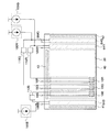
図1には、絶縁基板20上に、画素部40、信号線駆動回路43、第1の走査線駆動回路41、第2の走査線駆動回路42、モニター用回路64が設けられている。
In FIG. 1, a
画素部40には、複数の画素10が設けられ、各画素には、発光素子13、発光素子13に接続し、電流の供給を制御する機能を有するトランジスタ(以下、駆動用トランジスタと表記する)12が設けられている。発光素子は、電源18に接続されている。なお、より具体的な画素10の構成は、以下の実施の形態で例示する。
The
モニター用回路64には、モニター用発光素子66、モニター用発光素子66に接続されたトランジスタ(以下、モニター制御用トランジスタと表記する)111、モニター制御用トランジスタのゲート電極に出力端子が接続され、かつモニター制御用トランジスタの一方の電極及びモニター用発光素子に入力端子が接続されたインバーター112を有する。モニター制御用トランジスタ111には、モニター用電流線(以下、モニター線と表記する)113を介して、一定電流を供給する機能を有する定電流源105が接続されている。モニター制御用トランジスタ111は、複数のモニター用発光素子のそれぞれへ、モニター線からの電流供給を制御し、モニター線を介してショートしたモニター用発光素子へ供給される電流を電気的に遮断する機能を有する。インバーター112は、モニター用発光素子のいずれか一がショートするとき、モニター制御用トランジスタをオフとする機能を有する。モニター線は、複数のモニター用発光素子が有する電極に接続されているため、該電極の電位の変化をモニターする機能を有することができる。また定電流源は、モニター線へ一定電流を供給する機能を有すればよい。
The
モニター用発光素子66は、発光素子13と同一の作製条件により、同一の工程で作製されたものであり、同一構成を有する。そのため、環境温度の変化と経時劣化に対して同じ特性、又はほぼ同じ特性を有する。このようなモニター用発光素子66は、電源18に接続されている。ここで、発光素子13と接続される電源と、該モニター用発光素子66に接続される電源とは、同一電位のため、同一の符号を用いて、電源18と記載する。なお本実施の形態では、モニター制御用トランジスタ111の極性をpチャネル型として説明するが、これに限定されるものではなく、nチャネル型を用いてもよい。その場合、適宜周囲の回路構成を変更させる。
The monitor
このようなモニター用回路64を設ける位置は限定されず、信号線駆動回路43と画素部40との間や、第1又は第2の走査線駆動回路41、42と画素部40との間に設けてもよい。また信号線駆動回路や第1又は第2の走査線駆動回路は、絶縁基板上にCOGにより設けられたICチップを適用してもよい。
The position where such a
モニター用回路64と、画素部40との間には、バッファアンプ回路110が設けられている。バッファアンプ回路とは、入力と出力とが同じ電位であって、入力インピーダンスが高く、出力電流容量が高いという特性をもつ回路である。そのため、このような特性をもつ回路であれば、回路構成は適宜決定することができる。
A
このような構成において、バッファアンプ回路は、モニター用発光素子66の一方の電極の電位の変化に伴い、画素部40が有する発光素子13に印加する電圧を変化させる機能を有する。
In such a configuration, the buffer amplifier circuit has a function of changing a voltage applied to the
このような構成において、定電流源105、及びバッファアンプ回路110は同一な絶縁基板20上に設けても、別の基板上に設けてもよい。
In such a configuration, the constant
以上のような構成において、モニター用発光素子66には定電流源105から一定の電流が供給される。この状態で、環境温度の変化や、経時劣化が生じると、モニター用発光素子66の抵抗値が変化する。例えば、経時劣化が生じると、モニター用発光素子66の抵抗値が増加する。すると、モニター用発光素子66へ供給される電流値は一定であるため、モニター用発光素子66の両端の電位差が変化する。具体的には、モニター用発光素子66が有する両電極間の電位差が変化する。このとき、電源18に接続された電極の電位は固定されているため、定電流源105に接続されている電極の電位が変化する。この電極の電位の変化は、モニター線113を介してバッファアンプ回路110に供給される。
In the above configuration, a constant current is supplied from the constant
すなわち、バッファアンプ回路110の入力端子には、上記電極の電位の変化が入力される。また、バッファアンプ回路110の出力端子から出力される電位は、駆動用トランジスタ12を介して、発光素子13に供給される。具体的には、出力された電位は、発光素子13が有する電極の一方の電位として与えられる。
That is, the change in the potential of the electrode is input to the input terminal of the
このようにして、環境温度の変化や経時劣化の変化に応じたモニター用発光素子66の変化を、発光素子13にフィードバックする。その結果、発光素子13は、環境温度の変化や経時劣化の変化に応じた輝度で点灯することができる。従って、環境温度の変化や経時劣化の変化によらない表示を行うことができる発光装置を提供することができる。
In this way, a change in the monitor
さらに、複数のモニター用発光素子66を設けているため、これらの電位の変化を平均化して、発光素子13へ供給することができる。すなわち本発明において、モニター用発光素子66を複数設けることにより電位の変化を平均化することができ、好ましい。
Further, since a plurality of monitor
また複数のモニター用発光素子66を設けることにより、ショート等が生じたモニター用発光素子の代替を用意することができる。
Further, by providing a plurality of monitor
さらに本発明は、モニター用発光素子66に接続されたモニター制御用トランジスタ111及びインバーター112を設けたことを特徴とする。これはモニター用発光素子66の不良(初期不良や経時不良を含む)により生じる、モニター用回路64の動作不良を考慮して設けられている。例えば、定電流源105とモニター制御用トランジスタ111とが、その他のトランジスタ等を介さず接続されている場合、複数のモニター用発光素子のうち、あるモニター用発光素子66が、作製工程中の不良等により、モニター用発光素子が有する陽極と陰極とがショート(短絡)する場合を考える。すると、定電流源105からの電流は、モニター線113を介して、ショートしたモニター用発光素子66へ多く供給されてしまう。複数のモニター用発光素子は、それぞれ並列に接続されているため、ショートしたモニター用発光素子66へ多くの電流が供給されると、その他のモニター用発光素子には、所定の一定電流が供給されなくなる。その結果、適切なモニター用発光素子66の電位の変化を、発光素子13へ供給することができなくなってしまう。
Furthermore, the present invention is characterized in that a
このようなモニター用発光素子のショートは、該モニター用発光素子が有する陽極の電位と、陰極の電位とが同じとなる、または近づくことにより発生する。例えば、作製行程中、陽極と、陰極との間のゴミ等により、ショートすることがある。また、陽極と陰極とのショート以外にも、走査線と陽極がショートすること等により、モニター用発光素子がショートすることもある。 Such a short circuit of the light emitting element for monitoring occurs when the potential of the anode and the potential of the cathode of the light emitting element for monitoring become the same or approach each other. For example, a short circuit may occur due to dust or the like between the anode and the cathode during the manufacturing process. In addition to the short circuit between the anode and the cathode, the light emitting element for monitoring may be short circuited due to a short circuit between the scanning line and the anode.
そこで本発明は、モニター制御用トランジスタ111及びインバーター112を設けている。モニター制御用トランジスタ111は、上記のようなモニター用発光素子66のショート等による多量な電流の供給を防止するため、ショートしたモニター用発光素子66への電流の供給を止める、つまりショートしたモニター用発光素子と、モニター線とを電気的に遮断することを特徴とする。
Therefore, in the present invention, a
インバーター112は、複数のモニター用発光素子のいずれかがショートすると、モニター制御用トランジスタをオフとする電位を出力する機能を有する。加えてインバーター112は、複数のモニター用発光素子のいずれもショートしていないときには、モニター制御用トランジスタをオンとする電位を出力する機能を有する。
The
図5を用いて、モニター用回路64の詳しい動作を説明する。図5(A)に示すように、モニター用発光素子66が有する電極において、高電位側をアノード電極66a、低電位側をカソード電極66cとすると、アノード電極66aはインバーター112の入力端子に接続され、カソード電極66cは電源18に接続され、固定電位となる。そのため、モニター用発光素子66が有する陽極と陰極とがショートすると、アノード電極66aの電位が、カソード電極66cの電位に近づく。その結果、インバーター112には、カソード電極66cの電位に近い低電位が供給されるため、インバーター112が有するpチャネル型のトランジスタ112pがオンとなる。すると、高電位側の電位(Va)がインバーター112より出力され、モニター制御用トランジスタ111のゲート電位となる。すなわち、モニター制御用トランジスタ111のゲートに入力される電位はVaとなり、モニター制御用トランジスタ111はオフとなる。
The detailed operation of the
なお、高い側の電位(High)となるVDDは、アノード電位と同じか、アノード電位より高く設定する。また、インバーター112の低い側電位、電源18の電位、モニター線113の低い側電位、Vaに印加する低い側電位は、すべて等しくすることができる。一般的には、低い側電位は、グランドとする。だたしこれに限定されることはなく、低い側の電位は、高い側電位と、所定の電位差を有するように決定すればよい。所定の電位差は、発光材料の電流、電圧、輝度特性、または装置の仕様により決定することができる。
Note that the VDD that is the higher potential (High) is set to be equal to or higher than the anode potential. Further, the low side potential of the
ここで、モニター用発光素子66に一定電流を流す順序に注意する。モニター制御用トランジスタ111がオンの状態で、モニター線113に一定電流を流し始める必要がある。本実施の形態では、図5(B)に示すようにVaをLowにしたまま、モニター線113に電流を流し始めている。そしてVaは、モニター線113の電位が飽和状態となった後、VDDとなるようにする。その結果、モニター制御用トランジスタ111がオンの状態であっても、モニター線113を充電することができる。
Here, attention is paid to the order in which a constant current is supplied to the monitor
一方、モニター用発光素子66がショートしていない場合、アノード電極66aの電位がインバーター112に供給されるため、nチャネル型のトランジスタ112がオンとなる。すると、低電位側の電位がインバーター112より出力され、モニター制御用トランジスタ111はオンとなる。
On the other hand, when the monitor
このようにして、ショートしたモニター用発光素子66へは、定電流源105からの電流が、供給されないようにすることができる。従って、モニター用発光素子が複数ある場合、モニター用発光素子がショートしたとき、ショートしたモニター用発光素子への電流供給を遮断することでモニター線113の電位の変化を最小限に抑えることができる。その結果、適切なモニター用発光素子66の電位の変化を、発光素子13へ供給することができる。
In this way, the current from the constant
なお本実施の形態において、定電流源105は、一定の電流を供給することができる回路であればよく、例えばトランジスタを用いて作製することができる。
Note that in this embodiment mode, the constant
また本実施の形態では、モニター用回路64に複数のモニター用発光素子66、モニター制御用トランジスタ111、及びインバーター112を有するように説明したが、これに限定されない。例えばインバーター112は、モニター用発光素子がショートすると、それを検知して、モニター線113を介して、ショートしたモニター用発光素子へ供給される電流を遮断する機能を有していれば、どのような回路を用いてもよい。具体的には、ショートしたモニター用発光素子へ、供給される電流を遮断するため、モニター制御用トランジスタをオフとする機能を有していればよい。
In this embodiment, the
また本実施の形態では、複数のモニター用発光素子66を用いることを特徴とし、それらのいずれかが不良となっても、モニター動作を行うことができるため、好ましい。さらに、複数のモニター用発光素子で、モニター動作を平均化することができ、好ましい。 In this embodiment mode, a plurality of light emitting elements for monitoring 66 are used, which is preferable because a monitoring operation can be performed even if any of them is defective. Furthermore, the monitoring operation can be averaged with a plurality of monitoring light emitting elements, which is preferable.
本実施の形態において、バッファアンプ回路110は電位の変動を防止するために設けられている。従って、バッファアンプ回路110のように、電位の変動を防止することが可能な回路ならば、当該バッファアンプ回路110ではなく、別の回路を用いてもよい。すなわち、モニター用発光素子66の一方の電極の電位を発光素子13に伝達する際、モニター用発光素子66と発光素子13の間に、電位の変動を防止するための回路を設けるとき、そのような回路として、上記のバッファアンプ回路110に制約されず、どのような構成の回路を用いてもよい。
In this embodiment, the
(実施の形態2)
本実施の形態では、上記実施の形態と異なり、モニター用発光素子がショートしたときにモニター制御用トランジスタをオフとする回路構成及びその動作について説明する。
(Embodiment 2)
In this embodiment mode, a circuit configuration for turning off the monitor control transistor when the monitor light emitting element is short-circuited and the operation thereof will be described, unlike the above embodiment mode.
図6(A)に示すモニター用回路64は、pチャネル型の第1のトランジスタ80、第1のトランジスタにゲート電極が共通し、並列に接続されているnチャネル型の第2のトランジスタ81、第2のトランジスタに直列に接続されているnチャネル型の第3のトランジスタ82を有する。モニター用発光素子66は、第1及び第2のトランジスタ80、81のゲート電極に接続されている。モニター制御用トランジスタ111のゲート電極は、第1及び第2のトランジスタ80、81が互いに接続されている電極に接続されている。その他の構成は図5に示すモニター用回路64と同様である。
A
また、第1のpチャネル型のトランジスタ80の高電位側の電位をVaとし、第3のnチャネル型のトランジスタ82のゲート電極の電位をVbとする。そして、モニター線113の電位、Va、Vbの電位を図6(B)に示すように動作させる。
The potential on the high potential side of the first p-
まず、モニター線113の電位を飽和状態にさせ、その後、Vaの電位をHighとする。モニター用発光素子66がショートしている場合、モニター用発光素子66の陽極の電位、つまり点Dの電位は、モニター用発光素子66の陰極と、同程度にまで下がる。すると、第1及び第2のトランジスタ80、81のゲート電極には、低い電位、つまりLowが入力され、nチャネル型である第2のトランジスタ81がオフとなり、pチャネル型である第1のトランジスタ80がオンとなる。そして、第1のトランジスタ80の一方の電位である、高い側電位が、モニター制御用トランジスタ111のゲート電極へ入力され、オフとなる。その結果、ショートしたモニター用発光素子66には、モニター線113からの電流は供給されない。
First, the potential of the
このとき、ショートの状態がわずかであり、陽極の電位が微少に低下した場合であると、第1及び第2のトランジスタ80、81のいずれがオン、またはオフとなるか制御しづらいことがある。そこで、図6に示すように、第3のトランジスタ82のゲート電極へVbの電位を供給する。すなわち、図6(B)に示すように、VaがHighとなっている間に、Vbの電位をLowとする。すると、nチャネル型である第3のトランジスタ82はオフとなる。その結果、陽極の電位が、VDDから第1のトランジスタのしきい値電圧分下がった電位なら、第1のトランジスタ80をオンとすることができ、モニター制御用トランジスタ111をオフとすることができる。
At this time, if the short-circuit state is slight and the potential of the anode slightly decreases, it may be difficult to control which of the first and
このようにVbの電位を制御することにより、陽極の電位が、微少に下がった場合であっても、モニター制御用トランジスタ111を正確にオフとすることができる。
By controlling the potential of Vb in this way, the
なおモニター用発光素子が正常である場合、モニター制御用トランジスタ111がオンとなるように制御される。すなわち陽極の電位は、モニター線113の高電位とほぼ同じとなるため、第2のトランジスタ81がオンとなる。その結果、低電位がモニター制御用トランジスタ111のゲート電極に印加されるため、オンとなる。
When the monitor light emitting element is normal, the
また図7(A)に示すように、pチャネル型の第1のトランジスタ83と、第1のトランジスタに直列に接続される、pチャネル型の第2のトランジスタ84と、第2のトランジスタとゲート電極を共通とした、nチャネル型の第3のトランジスタ85と、第1のトランジスタとゲート電極を共通とし、並列に接続されるnチャネル型の第4のトランジスタ86とを有する。モニター用発光素子66は、第2及び第3のトランジスタ84、85のゲート電極に接続されている。モニター制御用トランジスタ111のゲート電極は、第2及び第3のトランジスタ84、85が互いに接続されている電極に接続されている。さらにモニター制御用トランジスタ111のゲート電極は、第4のトランジスタ86の一方の電極に接続されている。その他の構成は図5に示すモニター用回路64と同様である。
As shown in FIG. 7A, a p-channel
まず、モニター線113の電位を飽和状態にさせ、その後、Veの電位をLowとする。モニター用発光素子66がショートしている場合、モニター用発光素子66の陽極の電位、つまり点Dの電位は、モニター用発光素子66の陰極と、同程度にまで下がる。すると、第2及び第3のトランジスタ84、85のゲート電極には、低い電位、つまりLowが入力され、nチャネル型である第3のトランジスタ85がオフとなり、pチャネル型である第2のトランジスタ84がオンとなる。またVeの電位をLowとすると、第1のトランジスタ83はオンとなり、第4のトランジスタ86はオフとなる。そして、第2のトランジスタ84を介して、第1のトランジスタの高い側電位が、モニター制御用トランジスタ111のゲート電極へ入力され、オフとなる。その結果、ショートしたモニター用発光素子66には、モニター線113からの電流は供給されない。
First, the potential of the
このようにゲート電極の電圧Veを制御することにより、モニター制御用トランジスタ111を正確にオフとすることができる。
Thus, by controlling the voltage Ve of the gate electrode, the
(実施の形態3)
本発明において、発光素子及びモニター用発光素子に逆方向電圧を印加することができる。そこで本実施の形態では、逆方向電圧を印加する場合について説明する。
(Embodiment 3)
In the present invention, a reverse voltage can be applied to the light emitting element and the monitor light emitting element. Therefore, in this embodiment, a case where a reverse voltage is applied will be described.
逆方向電圧とは、発光素子13やモニター用発光素子66を発光させるときに印加する電圧を順方向電圧とすると、順方向電圧における高い側の電位と、低い側の電位とを反転させた電圧を印加することである。具体的にモニター用発光素子66を用いて説明すると、アノード電極66aと、カソード電極66cとの電位を反転させるため、電源18の電位より、モニター線113に印加する電位を低くすることである。
The reverse voltage is a voltage obtained by inverting a high-side potential and a low-side potential in a forward voltage when a voltage applied when the light-emitting
具体的には、図13に示すように、アノード電極66aの電位(アノード電位:Va)をHighからLowに反転させ、且つカソード電極66cの電位(カソード電位:Vc)をLowからHighに反転させる。このとき同時に、モニター線113の電位(V113)もHighからLowへ反転させる。このアノード電位及びカソード電位が反転している期間を、逆方向電圧印加期間という。そして、所定の逆方向電圧印加期間経過後、カソード電位をHighからLowへ戻すと、モニター線113に一定電流が流れはじめ、充電が完了する。充電が完了した、つまりモニター線113の電圧がHighとなった後、アノード線の電位をLowからHighへ戻す。このとき、モニター線113の電位が時間と共に曲線状に戻るのは、一定電流で複数のモニター用発光素子を充電し、さらには寄生容量を充電することによる。
Specifically, as shown in FIG. 13, the potential of the
好ましくは、アノード電位を反転させ、次いでカソード電位を反転させるとよい。そして所定の逆方向電圧期間経過後、アノード電位を戻し、次いでカソード電位を戻す。そしてアノード電位の反転と同時に、モニター線113の電位をHighに充電とする。
Preferably, the anode potential is inverted, and then the cathode potential is inverted. Then, after a predetermined reverse voltage period has elapsed, the anode potential is returned, and then the cathode potential is returned. Simultaneously with the reversal of the anode potential, the potential of the
この逆方向電圧印加期間では、駆動用トランジスタ12及びモニター制御用トランジスタ111がオンとなっていなければならない。
In this reverse voltage application period, the driving
逆方向電圧を発光素子へ印加する結果、発光素子13、加えてモニター用発光素子66の不良状態を改善し、信頼性を向上させることができる。また、発光素子13、加えてモニター用発光素子66は、異物の付着や、陽極又は陰極にある微細な突起によるピンホール、電界発光層の不均一性を起因として、陽極と陰極がショートする初期不良が生じることがある。このような初期不良が発生すると、信号に応じた点灯及び非点灯が行われず、電流のほとんどがショートした素子を流れてしまう。その結果、画像の表示が良好に行われないという問題が発生する。また、この不良は任意の画素に生じる恐れがある。
As a result of applying the reverse voltage to the light emitting element, the defective state of the
そこで本実施の形態のように、発光素子13、加えてモニター用発光素子66に逆方向電圧を印加すると、ショートした部分に局所的な電流が流れ、該ショートした部分が発熱し、酸化又は炭化させることができる。その結果、ショートした部分を絶縁化させることができ、その部分以外の領域に電流が流れ、発光素子13又はモニター用発光素子66として、正常に動作させることが可能となる。このように逆方向電圧を印加することにより、初期不良が生じても、その不良を解消することができる。なお、このような短絡部の絶縁化は、出荷前に行うとよい。
Therefore, as in the present embodiment, when a reverse voltage is applied to the
また、初期不良だけでなく、時間の経過に伴い、新たに陽極と陰極のショートが発生することがある。このような不良は、進行性不良とも呼ばれる。そこで本発明のように、定期的に発光素子13、加えてモニター用発光素子66に逆方向電圧を印加することにより、進行性不良が生じても、その不良を解消することができ、発光素子13又はモニター用発光素子66として、正常に動作させることが可能となる。
In addition to the initial failure, a short circuit between the anode and the cathode may occur as time passes. Such a defect is also called a progressive defect. Therefore, as in the present invention, by applying a reverse voltage to the
また加えて、逆方向電圧を印加することによって、画像の焼き付きを防止することができる。画像の焼き付きとは、発光素子13の劣化状態により生じるが、逆方向電圧を印加することにより、劣化状態を低減することができる。その結果、画像の焼き付きが防止できる。
In addition, image burn-in can be prevented by applying a reverse voltage. Image burn-in occurs due to the deterioration state of the
また一般に発光素子13、加えてモニター用発光素子66の劣化は、初期に大きく進み、時間と共に劣化の進行度合いが少なくなってくる。すなわち画素において、一度劣化した発光素子13やモニター用発光素子66は、さらなる劣化が生じにくくなる。その結果、各発光素子13にバラツキが生じる。そのため、出荷前、又は画像を表示しないとき等に、すべての発光素子13、さらにはモニター用発光素子66を点灯し、劣化していない素子に劣化を生じさせることによって、全素子の劣化状態を平均化することができる。このような、全素子を点灯する構成を発光装置に設けてもよい。
In general, the deterioration of the
(実施の形態4)
本実施の形態では、画素回路及び構成の一例について説明する。
(Embodiment 4)
In this embodiment, an example of a pixel circuit and a structure is described.
図2には、本発明の画素部に用いることのできる画素回路を示す。画素部40は、信号線Sx、走査線Gy、電源線Vxがマトリックス状に設けられており、それらの交点には画素10が設けられている。画素10は、スイッチング用トランジスタ11、駆動用トランジスタ12、容量素子16、発光素子13を有する。
FIG. 2 shows a pixel circuit that can be used in the pixel portion of the present invention. In the
当該画素における接続関係を説明する。スイッチング用トランジスタ11は、信号線Sxと、走査線Gyとの交点に設けられ、スイッチング用トランジスタ11の一方の電極は信号線Sxと、スイッチング用トランジスタ11のゲート電極は走査線Gyと接続されている。駆動用トランジスタ12は、一方の電極が電源線Vxに接続され、ゲート電極はスイッチング用トランジスタ11の他方の電極と接続されている。容量素子16は、駆動用トランジスタ12のゲート・ソース間電圧を保持するように設けられている。本実施の形態では、容量素子16は、その一方の電極はVxに、他方の電極は駆動用トランジスタ12のゲート電極に接続されている。なお、容量素子16は、駆動用トランジスタ12のゲート容量が大きく、リーク電流が少ない場合等は設ける必要がない。発光素子13は、駆動用トランジスタ12の他方の電極に接続されている。
A connection relationship in the pixel will be described. The switching
このような画素の駆動方法について説明する。 A method for driving such a pixel will be described.
まず、スイッチング用トランジスタ11がオンとなると、信号線Sxからビデオ信号が入力される。ビデオ信号に基づき、容量素子16に電荷が蓄積される。容量素子16に蓄積された電荷が、駆動用トランジスタ12のゲート・ソース間電圧(Vgs)を越えると、駆動用トランジスタ12がオンとなる。すると、発光素子13に電流が供給され、点灯する。このとき、駆動用トランジスタ12は、線形領域又は飽和領域で動作させることができる。飽和領域で動作させると、一定の電流を供給することができる。また線形領域で動作させると、低電圧で動作させることができ、低消費電力化を図ることができる。
First, when the switching
以下に、タイミングチャートを用いて、画素の駆動方法について説明する。 Hereinafter, a pixel driving method will be described with reference to a timing chart.
図8(a)には、1秒間に60フレームの画像の書き換えが行われる場合のある1フレーム期間のタイミングチャートを示す。該タイミングチャートにおいて、縦軸は走査線G(1行目から最終行目)、横軸は時間を示している。 FIG. 8A shows a timing chart of one frame period in which an image of 60 frames is rewritten in one second. In the timing chart, the vertical axis indicates the scanning line G (from the first line to the last line), and the horizontal axis indicates time.
1フレーム期間はm(mは2以上の自然数)個のサブフレーム期間SF1、SF2、…、SFmを有し、m個のサブフレーム期間SF1、SF2、…SFmは、それぞれ書き込み動作期間Ta1、Ta2、…、Tamと表示期間(点灯期間)Ts1、Ts2、…、Tsmと、逆方向電圧印加期間とを有する。本実施の形態では、図8(A)に示すように、1フレーム期間は、サブフレーム期間SF1、SF2、及びSF3と、逆方向電圧印加期間(FRB)とが設けられている。そして、各サブフレーム期間は、書き込み動作期間Ta1〜Ta3が順に行われ、それぞれ表示期間Ts1〜Ts3となる。 One frame period has m (m is a natural number of 2 or more) subframe periods SF1, SF2,..., SFm, and the m subframe periods SF1, SF2,. ,..., Tam, a display period (lighting period) Ts1, Ts2,..., Tsm, and a reverse voltage application period. In this embodiment mode, as shown in FIG. 8A, in one frame period, subframe periods SF1, SF2, and SF3 and a reverse voltage application period (FRB) are provided. In each subframe period, the writing operation periods Ta1 to Ta3 are sequentially performed, and become display periods Ts1 to Ts3, respectively.
図8(B)に記載のタイミングチャートには、ある行(i行目)に着目したときの、書き込み動作期間、表示期間、及び逆方向電圧印加期間について示す。書き込み動作期間、表示期間が交互に現れた後、逆方向電圧印加期間が現れる。この書き込み動作期間、及び表示期間を有する期間が、順方向電圧印加期間となる。 The timing chart illustrated in FIG. 8B illustrates a writing operation period, a display period, and a reverse voltage application period when attention is paid to a certain row (i-th row). After the writing operation period and the display period appear alternately, a reverse voltage application period appears. The period having the writing operation period and the display period is a forward voltage application period.
書き込み動作期間Taは複数の動作期間に分けることができる。本実施の形態では、二つの動作期間に分け、一方で消去動作を行い、他方で書き込み動作を行う。このように消去動作と、書き込み動作を設けるため、WE(Write Erase)信号が入力される。その他の消去動作及び書き込み動作や信号の詳細は、以下の実施の形態で説明する。 The write operation period Ta can be divided into a plurality of operation periods. In the present embodiment, the operation is divided into two operation periods, and an erase operation is performed on the one hand and a write operation is performed on the other hand. In order to provide the erase operation and the write operation in this way, a WE (Write Erase) signal is input. Details of other erase operations, write operations, and signals will be described in the following embodiments.
また、逆方向電圧印加期間の直前には、全画素のスイッチング用トランジスタを同時にオンとする期間、つまり全走査線をオンとする期間(オン期間)を設ける。 Further, immediately before the reverse voltage application period, a period in which the switching transistors of all the pixels are simultaneously turned on, that is, a period in which all the scanning lines are turned on (on period) is provided.
逆方向電圧印加期間の直後には、全画素のスイッチング用トランジスタを同時にオフとする期間、つまり全走査線をオフとする期間(オフ期間)を設けるとよい。 Immediately after the reverse voltage application period, a period in which the switching transistors of all the pixels are simultaneously turned off, that is, a period in which all the scanning lines are turned off (off period) may be provided.
また、逆方向電圧印加期間の直前には、消去期間(SE)が設けられている。消去期間は、上記消去動作と同様な動作により行うことができる。消去期間は、直前のサブフレーム期間、本実施の形態ではSF3で書き込まれたデータを、順に消去する動作が順次行われる。なぜなら、オン期間では、最終行目の画素の表示期間が終了後、一斉にスイッチング用トランジスタをオンとするため、1行目等の画素は、不要な表示期間を有することになるからである。 An erasing period (SE) is provided immediately before the reverse voltage application period. The erasing period can be performed by the same operation as the erasing operation. In the erasing period, an operation of sequentially erasing data written in SF3 in the immediately preceding subframe period, in this embodiment, is sequentially performed. This is because in the on period, the switching transistors are turned on all at once after the display period of the pixels in the last row ends, and thus the pixels in the first row and the like have an unnecessary display period.
このように、オン期間、オフ期間、消去期間を設けるための制御は、走査線駆動回路や信号線駆動回路等の駆動回路によって行われる。 In this manner, control for providing the on period, the off period, and the erasing period is performed by a driving circuit such as a scanning line driving circuit or a signal line driving circuit.
なお、発光素子13に逆方向電圧の電圧を印加するタイミング、つまり逆方向電圧印加期間は、図8(A)(B)に限定されない。すなわち、フレーム毎に逆方向電圧印加期間を設ける必要はない。また1フレームの後半に逆方向電圧印加期間を設ける必要もない。またオン期間は、少なくとも印加期間(RB)の直前にあればよく、オフ期間は少なくとも印加期間(RB)直後にあればよい。また発光素子の陽極の電位と、陰極の電位とを逆にする順序も図8(A)(B)に限定されない。すなわち、陰極の電位を上げた後、陽極の電位を下げてもよい。
Note that the timing of applying the reverse voltage to the
図3には、図2に示した画素回路のレイアウト例を示す。スイッチング用トランジスタ11、駆動用トランジスタ12を構成する半導体膜を形成する。その後、ゲート絶縁膜として機能する絶縁膜を介して、第1の導電膜を形成する。該導電膜は、スイッチング用トランジスタ11、駆動用トランジスタ12のゲート電極として用い、また走査線Gyとして用いることができる。このとき、スイッチング用トランジスタ11は、ダブルゲート構造とするとよい。
FIG. 3 shows a layout example of the pixel circuit shown in FIG. A semiconductor film constituting the switching
その後、層間絶縁膜として機能する絶縁膜を介して、第2の導電膜を形成する。該導電膜は、スイッチング用トランジスタ11、駆動用トランジスタ12のドレイン配線、及びソース配線として用い、また信号線Sx、電源線Vxとしてもちいることができる。このとき、容量素子16は、第1の導電膜、層間絶縁膜として機能する絶縁膜、第2の導電膜の積層構造により形成することができる。駆動用トランジスタ12のゲート電極と、スイッチング用トランジスタの他方の電極とは、コンタクトホールを介して接続される。
After that, a second conductive film is formed through an insulating film functioning as an interlayer insulating film. The conductive film can be used as a drain wiring and a source wiring of the switching
そして、画素に設けられた開口部には、画素電極19を形成する。該画素電極は、駆動用トランジスタ12の他方の電極に接続されている。このとき、第2の導電膜と画素電極との間に絶縁膜等が設けられている場合、コンタクトホールを介して接続する必要がある。絶縁膜等が設けられていない場合、駆動用トランジスタ12の他方の電極に、画素電極が直接接続することができる。
A
図3に示すようなレイアウトにおいて、高開口率を確保するため、領域430のように、第1の導電膜と、画素電極とが重なってしまうことがある。そのような領域430には、結合容量が生じてしまうことがある。この結合容量は不要な容量である。このような不要な容量は、本発明の駆動方法によって、除去することができる。
In the layout as illustrated in FIG. 3, the first conductive film and the pixel electrode may overlap as in the
図4には、図3に示したA−B、B−Cの断面図例を示す。 FIG. 4 shows a cross-sectional example of AB and BC shown in FIG.
絶縁基板20上には、下地膜を介して、パターニングされた半導体膜が形成されている。絶縁基板20には、例えばバリウムホウケイ酸ガラスや、アルミノホウケイ酸ガラスなどのガラス基板、石英基板、ステンレス(SUS)基板等を用いることができる。また、PET(ポリエチレンテレフタレート)、PEN(ポリエチレンナフタレート)、PES(ポリエーテルスルホン)に代表されるプラスチックや、アクリル等の可撓性を有する合成樹脂からなる基板は、一般的に他の基板と比較して耐熱温度が低い傾向にあるが、作製工程における処理温度に耐え得るのであれば用いることが可能である。下地膜には、酸化珪素や、窒化珪素、窒化酸化珪素などの絶縁膜を用いることができる。
A patterned semiconductor film is formed on the insulating
下地膜上に非晶質半導体膜を形成する。非晶質半導体膜の膜厚は25〜100nm(好ましくは30〜60nm)とする。また非晶質半導体は珪素だけではなくシリコンゲルマニウムも用いることができる。 An amorphous semiconductor film is formed over the base film. The thickness of the amorphous semiconductor film is 25 to 100 nm (preferably 30 to 60 nm). As the amorphous semiconductor, not only silicon but also silicon germanium can be used.
次に、必要に応じて非晶質半導体膜を結晶化し、結晶性半導体膜を形成する。結晶化する方法は、加熱炉、レーザ照射、若しくはランプから発する光の照射(以下、ランプアニールと表記する)、又はそれらを組み合わせて用いることができる。例えば、非晶質半導体膜に金属元素を添加し、加熱炉を用いた熱処理を行うことによって結晶性半導体膜を形成する。このように、金属元素を添加することにより、低温で結晶化できるため好ましい。 Next, the amorphous semiconductor film is crystallized as necessary to form a crystalline semiconductor film. As a method for crystallization, a heating furnace, laser irradiation, irradiation with light emitted from a lamp (hereinafter referred to as lamp annealing), or a combination thereof can be used. For example, a crystalline semiconductor film is formed by adding a metal element to an amorphous semiconductor film and performing heat treatment using a heating furnace. Thus, it is preferable to add a metal element because crystallization can be performed at a low temperature.
このように形成された結晶性半導体膜を、所定の形状にパターニングする。所定の形状とは、図3で示したように、スイッチング用トランジスタ11、駆動用トランジスタ12となる形状である。
The crystalline semiconductor film thus formed is patterned into a predetermined shape. The predetermined shape is a shape that becomes the switching
次いで、ゲート絶縁膜として機能する絶縁膜を形成する。該絶縁膜は、半導体膜を覆うように、厚さを10〜150nm、好ましくは20〜40nmとして形成される。例えば、酸化窒化珪素膜、酸化珪素膜等を用いることができ、単層構造または積層構造としてもよい。 Next, an insulating film functioning as a gate insulating film is formed. The insulating film is formed so as to cover the semiconductor film with a thickness of 10 to 150 nm, preferably 20 to 40 nm. For example, a silicon oxynitride film, a silicon oxide film, or the like can be used, and a single layer structure or a stacked structure may be used.
そしてゲート絶縁膜を介して、ゲート電極として機能する第1の導電膜を形成する。ゲート電極は、単層であっても積層であってもよいが、本実施の形態では導電膜22a、22bの積層構造を用いる。各導電膜22a、22bは、Ta、W、Ti、Mo、Al、Cuから選ばれた元素、または前記元素を主成分とする合金材料もしくは化合物材料で形成すればよい。本実施の形態では、導電膜22aとして膜厚10〜50nm、例えば30nmの窒化タンタル膜を形成し、導電膜22bとして膜厚200〜400nm、例えば370nmのタングステン膜を順次形成する。
Then, a first conductive film functioning as a gate electrode is formed through the gate insulating film. Although the gate electrode may be a single layer or a stacked layer, in this embodiment mode, a stacked structure of
ゲート電極をマスクとして不純物元素を添加する。このとき、高濃度不純物領域に加えて、低濃度不純物領域を形成してもよい。これをLDD(Lightly Doped Drain)構造という。特に低濃度不純物領域がゲート電極と重なった構造をGOLD(Gate−drain Overlapped LDD)構造という。特に、nチャネル型トランジスタは、低濃度不純物領域を有する構成とするとよい。 An impurity element is added using the gate electrode as a mask. At this time, a low concentration impurity region may be formed in addition to the high concentration impurity region. This is referred to as an LDD (Lightly Doped Drain) structure. In particular, a structure in which a low-concentration impurity region overlaps with a gate electrode is referred to as a GOLD (Gate-drain Overlapped LDD) structure. In particular, the n-channel transistor may have a low concentration impurity region.
この低濃度不純物領域に起因して、不要な容量が形成されてしまうこともある。そのため、LDD構造やGOLD構造を有するTFTを用いて画素を形成する場合、本発明の駆動方法を用いると好適である。 An unnecessary capacitance may be formed due to the low concentration impurity region. Therefore, when a pixel is formed using a TFT having an LDD structure or a GOLD structure, it is preferable to use the driving method of the present invention.
その後、層間絶縁膜30として機能する絶縁膜28、29を形成する。絶縁膜28は、窒素を有する絶縁膜であればよく、本実施の形態では、プラズマCVD法により100nmの窒化珪素膜を用いて形成する。また絶縁膜29は、有機材料又は無機材料を用いて形成することができる。有機材料としては、ポリイミド、アクリル、ポリアミド、ポリイミドアミド、レジスト又はベンゾシクロブテン、シロキサン、ポリシラザンを用いることができる。なお、シロキサンとは、Si−O−Si結合を含む樹脂に相当する。シロキサンは、シリコン(Si)と酸素(O)との結合で骨格構造が構成される。置換基として、少なくとも水素を含む有機基(例えばアルキル基、芳香族炭化水素)が用いられる。または置換基として、フルオロ基を用いてもよい。または置換基として、少なくとも水素を含む有機基と、フルオロ基とを用いてもよい。またポリシラザンとは、珪素(Si)と窒素(N)の結合を有するポリマー材料、いわゆるポリシラザンを含む液体材料を出発原料として形成される。無機材料としては、酸化珪素(SiOx)、窒化珪素(SiNx)、酸化窒化珪素(SiOxNy)(x>y)、窒化酸化珪素(SiNxOy)(x>y)(x、y=1、2・・・)等の酸素、又は窒素を有する絶縁膜を用いることができる。また、第2の絶縁膜107として、これら絶縁膜の積層構造を用いてもよい。特に、有機材料を用いて第2の層間絶縁膜を形成すると、平坦性は高まる一方で、有機材料によって水分や酸素が吸収されてしまう。これを防止するため、有機材料上に、無機材料を有する絶縁膜を形成するとよい。無機材料に、窒素を有する絶縁膜を用いると、Na等のアルカリイオンの侵入を防ぐことができ、好ましい。絶縁膜29に、有機材料を用いると平坦性を高めることができ、好ましい。
Thereafter, insulating
層間絶縁膜30にコンタクトホールを形成する。そして、スイッチング用トランジスタ11、駆動用トランジスタ12のソース配線及びドレイン配線24、信号線Sx、電源線Vxとして機能する第2の導電膜を形成する。第2の導電膜は、アルミニウム(Al)、チタン(Ti)、モリブデン(Mo)、タングステン(W)もしくはシリコン(Si)の元素からなる膜又はこれらの元素を用いた合金膜を用いることができる。本実施の形態では、チタン膜/窒化チタン膜/アルミニウムとシリコンとを有する膜/チタン膜(Ti/TiN/Al−Si/Ti)をそれぞれ60/40/300/100nmに積層して第2の導電膜を形成する。
Contact holes are formed in the
その後、第2の導電膜を覆うように絶縁膜31を形成する。絶縁膜31は、層間絶縁膜30で示した材料を用いることができる。このように絶縁膜31を設けることにより、開口率を高めることができる。
Thereafter, an insulating
そして、絶縁膜31に設けられた開口部に画素電極(第1の電極ともいう)19を形成する。該開口部において、画素電極の段差被覆性を高めるため、開口部端面に、複数の曲率半径を有するように丸みを帯びさせるとよい。画素電極19には、透光性を有する材料として、インジウム錫酸化物(ITO、indiumu Tin Oxide)、酸化インジウムに2〜20atom%の酸化亜鉛(ZnO)を混合したIZO(indium zinc oxide)、酸化インジウムに2〜20atom%の酸化珪素(SiO2)を混合したITO−SiOx(便宜上ITSOと表記する)、有機インジウム、有機スズ等を用いることもできる。また非透光性を有する材料として、銀(Ag)以外にタンタル、タングステン、チタン、モリブデン、アルミニウム、銅から選ばれた元素、又は前記元素を主成分とする合金材料もしくは化合物材料を用いることができる。このとき、有機材料を用いて絶縁膜31を形成し、平坦性を高めると、画素電極形成面の平坦性が向上するため、均一な電圧を印加でき、さらには短絡を防止することができる。
Then, a pixel electrode (also referred to as a first electrode) 19 is formed in the opening provided in the insulating
第1の導電膜と、画素電極とが重なってしまう領域430には、結合容量が生じてしまうことがある。この結合容量は不要な容量である。このような不要な容量は、本発明の駆動方法によって、除去することができる。
In a
その後、蒸着法、またはインクジェット法により電界発光層33を形成する。電界発光層140は、有機材料、又は無機材料を有し、電子注入層(EIL)、電子輸送層(ETL)、発光層(EML)、正孔輸送層(HTL)、正孔注入層(HIL)等を適宜組み合わせて構成される。なお各層の境目は必ずしも明確である必要はなく、互いの層を構成している材料が一部混合し、界面が不明瞭になっている場合もある。また、電界発光層は上記積層構造に限定されない。
Thereafter, the
そして、スパッタリング法、又は蒸着法により第2の電極35を形成する。電界発光層(発光素子)の第1の電極(画素電極)19、及び第2の電極35は、画素構成により陽極又は陰極となる。
Then, the
陽極材料としては、仕事関数の大きい(仕事関数4.0eV以上)金属、合金、電気伝導性化合物、およびこれらの混合物などを用いることが好ましい。陽極材料の具体例としては、ITO、酸化インジウムに2〜20%の酸化亜鉛(ZnO)を混合したIZOの他、金(Au)、白金(Pt)、ニッケル(Ni)、タングステン(W)、クロム(Cr)、モリブデン(Mo)、鉄(Fe)、コバルト(Co)、銅(Cu)、パラジウム(Pd)、または金属材料の窒化物(TiN)等を用いることができる。 As the anode material, it is preferable to use a metal, an alloy, an electrically conductive compound, a mixture thereof, or the like having a high work function (work function of 4.0 eV or more). Specific examples of anode materials include ITO, IZO mixed with 2-20% zinc oxide (ZnO) in indium oxide, gold (Au), platinum (Pt), nickel (Ni), tungsten (W), Chromium (Cr), molybdenum (Mo), iron (Fe), cobalt (Co), copper (Cu), palladium (Pd), nitride of metal material (TiN), or the like can be used.
一方、陰極材料としては、仕事関数の小さい(仕事関数3.8eV以下)金属、合金、電気伝導性化合物、およびこれらの混合物などを用いることが好ましい。陰極材料の具体例としては、元素周期律の1族または2族に属する元素、すなわちLiやCs等のアルカリ金属、およびMg、Ca、Sr等のアルカリ土類金属、およびこれらを含む合金(Mg:Ag、Al:Li)や化合物(LiF、CsF、CaF2)の他、希土類金属を含む遷移金属を用いて形成することができる。但し、陰極は透光性を有する必要があるため、これら金属、又はこれら金属を含む合金を非常に薄く形成し、ITO等の金属(合金を含む)との積層により形成する。 On the other hand, as the cathode material, it is preferable to use a metal, an alloy, an electrically conductive compound, a mixture thereof, or the like having a low work function (work function of 3.8 eV or less). Specific examples of the cathode material include elements belonging to Group 1 or Group 2 of the element periodic rule, that is, alkali metals such as Li and Cs, and alkaline earth metals such as Mg, Ca, and Sr, and alloys containing these (Mg : Ag, Al: Li) and compounds (LiF, CsF, CaF 2 ), as well as transition metals including rare earth metals. However, since the cathode needs to have translucency, these metals or an alloy containing these metals are formed very thinly, and are formed by lamination with a metal (including an alloy) such as ITO.
上記の材料のうち非透光性材料は、その膜厚を薄くすることによって透明電極として適用することができる。 Among the above materials, the non-translucent material can be applied as a transparent electrode by reducing the film thickness.
その後、第2の電極35を覆って、保護膜を形成してもよい。保護膜としては、窒化珪素膜やDLC膜を用いることができる。
Thereafter, a protective film may be formed to cover the
このようにして、発光装置の画素を形成することができる。 In this manner, a pixel of the light emitting device can be formed.
(実施の形態5)
本実施の形態では、上記実施の形態で示した画素回路を有するパネル全体の構成について説明する。
(Embodiment 5)
In this embodiment, a structure of the entire panel including the pixel circuit described in the above embodiment is described.
図12に示すように、本発明の発光装置は、上述した画素10がマトリクス状に複数配置された画素部40と、第1の走査線駆動回路41と、第2の走査線駆動回路42と、信号線駆動回路43とを有する。第1の走査線駆動回路41と第2の走査線駆動回路42は、画素部40を挟んで対向するように配置するか、画素部40の上下左右の四方のうち一方に配置するとよい。
As shown in FIG. 12, the light-emitting device of the present invention includes a
信号線駆動回路43は、パルス出力回路44、ラッチ45及び選択回路46を有する。ラッチ45は第1のラッチ47と第2のラッチ48を有する。選択回路46は、スイッチング手段としてトランジスタ49(以下TFT49と表記)と、アナログスイッチ50とを有する。TFT49とアナログスイッチ50は、信号線に対応して、各列に設けられている。加えて、本実施の形態では、WE信号の反転信号を生成するために、インバーター51が各列に設けられている。なおインバーター51は、外部からWE信号の反転信号を供給する場合には設けなくてもよい。
The signal
TFT49のゲート電極は選択信号線52に接続し、一方の電極は信号線に接続し、他方の電極は電源53に接続する。アナログスイッチ50は、第2のラッチ48と各信号線の間に設けられる。すなわち、アナログスイッチ50の入力端子は第2のラッチ48に接続し、出力端子は信号線に接続する。アナログスイッチ50の2つの制御端子は、一方は選択信号線52に接続し、他方はインバーター51を介して選択信号線52に接続する。電源53の電位は、画素が有する駆動用トランジスタ12をオフにする電位であり、駆動用トランジスタ12の極性がnチャネル型の場合は電源53の電位をLowとし、駆動用トランジスタ12がpチャネル型の場合は電源53の電位をHighとする。
The gate electrode of the
第1の走査線駆動回路41はパルス出力回路54と選択回路55を有する。第2の走査線駆動回路42はパルス出力回路56と選択回路57を有する。パルス出力回路54、56には、それぞれスタートパルス(G1SP、G2SP)が入力される。またパルス出力回路54、56にはそれぞれクロックパルス(G1CK、G2CK)と、それの反転クロックパルス(G1CKB、G2CKB)が入力される。
The first scanning
選択回路55、57は、選択信号線52に接続する。但し、第2の走査線駆動回路42が含む選択回路57は、インバーター58を介して選択信号線52に接続する。つまり、選択信号線52を介して、選択回路55、57に入力されるWE信号は、互いに反転した関係にある。
The
選択回路55、57の各々はトライステートバッファを有する。トライステートバッファは、選択信号線52から伝達される信号がHレベルのときに動作状態となり、Lレベルのときにハイインピーダンス状態となる。
Each of the
信号線駆動回路43が含むパルス出力回路44、第1の走査線駆動回路41が含むパルス出力回路54、第2の走査線駆動回路42が含むパルス出力回路56は、複数のフリップフロップ回路からなるシフトレジスタやデコーダ回路を有する。パルス出力回路44、54、56として、デコーダ回路を適用すれば、信号線又は走査線をランダムに選択することができる。信号線又は走査線をランダムに選択することができると、時間階調方式を適用した場合に生じる疑似輪郭の発生を抑制することができる。
The
なお信号線駆動回路43の構成は上記の記載に制約されず、レベルシフタやバッファを設けてもよい。また、第1の走査線駆動回路41と第2の走査線駆動回路42の構成も上記の記載に制約されず、レベルシフタやバッファを設けてもよい。また、信号線駆動回路43、第1の走査線駆動回路41、又は第2の走査線駆動回路42は、それぞれ保護回路を有してもよい。
Note that the configuration of the signal
また本発明において、保護回路を設けてもよい。保護回路は、複数の抵抗素子を有するように形成することができる。例えば複数の抵抗素子として、pチャネル型のトランジスタを用いることができる。保護回路は、信号線駆動回路43、第1の走査線駆動回路41、又は第2の走査線駆動回路42にそれぞれ設けることができ、好ましくは、信号線駆動回路43、第1の走査線駆動回路41、又は第2の走査線駆動回路42と画素部40との間に設けるとよい。このような保護回路により、静電気に起因した素子の劣化や破壊を抑制することができる。
In the present invention, a protection circuit may be provided. The protection circuit can be formed to have a plurality of resistance elements. For example, p-channel transistors can be used as the plurality of resistance elements. The protection circuit can be provided in each of the signal
また本実施の形態において、発光装置は電源制御回路63を有する。電源制御回路63は、発光素子13に電源を供給する電源回路61とコントローラ62を有する。電源回路61は、第1の電源17を有し、第1の電源17は駆動用トランジスタ12と電源線Vxを介して発光素子13の画素電極に接続する。また、電源回路61は、第2の電源18を有し、第2の電源18は対向電極に接続される電源線を介して、発光素子13に接続する。
In this embodiment mode, the light emitting device has a power
このような電源回路61は、発光素子13に順方向電圧を印加して、発光素子13に電流を流して発光させるときは、第1の電源17の電位が、第2の電源18の電位よりも高くなるように設定する。一方、発光素子13に逆方向電圧を印加するときは、第1の電源17の電位が、第2の電源18の電位よりも低くなるように設定する。このような電源の設定は、コントローラ62から電源回路61に所定の信号を供給することにより、行うことができる。
In such a
また本実施の形態において、発光装置は、モニター用回路64と制御回路65を有することを特徴とする。制御回路65は定電流源とバッファアンプ回路を有する。また、モニター用回路64は、モニター用発光素子66、モニター制御用トランジスタ111、インバーター112を有する。
In this embodiment mode, the light-emitting device includes a
制御回路65は、モニター用回路64の出力に基づき、電源電位を補正する信号を、電源制御回路63に供給する。電源制御回路63は、制御回路65から供給される信号に基づき、画素部40に供給する電源電位を補正する。
The
上記構成を有する本発明の発光装置は、環境温度の変化や経時劣化に起因した電流値の変動を抑制して、信頼性を向上させることができる。さらにモニター制御用トランジスタ111及びインバーター112により、ショートしたモニター用発光素子66に、定電流源105からの電流が流れることを防止でき、正確な電流値の変動を発光素子13へ供給することができる。
The light emitting device of the present invention having the above structure can improve the reliability by suppressing the fluctuation of the current value due to the change of the environmental temperature or the deterioration with time. Further, the
(実施の形態6)
本実施の形態では、上記構成を有する本発明の発光装置の動作について図面を参照して説明する。
(Embodiment 6)
In this embodiment mode, operation of the light-emitting device of the present invention having the above structure is described with reference to drawings.
まず、信号線駆動回路43の動作について図14(A)を用いて説明する。パルス出力回路44には、クロック信号(以下SCKと表記)、クロック反転信号(以下SCKBと表記)及びスタートパルス(以下SSPと表記)が入力され、これらの信号のタイミングに従って、第1のラッチ47にサンプリングパルスを出力する。データが入力される第1のラッチ47は、サンプリングパルスが入力されるタイミングに従って、1列目から最終列目までビデオ信号を保持する。第2のラッチ48は、ラッチパルスが入力されると、第1のラッチ47に保持されていたビデオ信号を、一斉に第2のラッチ48に転送する。
First, operation of the signal
ここで、選択信号線52から伝達されるWE信号がLレベルのときを期間T1とし、WE信号がHレベルのときを期間T2として、各期間における選択回路46の動作について説明する。期間T1、T2は水平走査期間の半分の期間に相当し、期間T1を第1のサブゲート選択期間、期間T2を第2のサブゲート選択期間とよぶ。
Here, the operation of the
期間T1(第1のサブゲート選択期間)において、選択信号線52から伝達されるWE信号はLレベルであり、トランジスタ49はオン状態、アナログスイッチ50は非導通状態となる。そうすると、複数の信号線S1〜Snは、各列に配置されたトランジスタ49を介して、電源53と電気的に接続する。つまり、複数の信号線Sxは、電源53と同電位になる。このとき、選択された画素10が有するスイッチング用トランジスタ11は、オンとなっており、当該スイッチング用トランジスタ11を介して、電源53の電位が駆動用トランジスタ12のゲート電極に伝達される。そうすると、駆動用トランジスタ12はオフ状態となり、発光素子13が有する両電極間には電流が流れず非発光となる。このように、信号線Sxに入力されるビデオ信号の状態に関係なく、電源53の電位が駆動用トランジスタ12のゲート電極に伝達されて、当該スイッチング用トランジスタ11がオフ状態になり、発光素子13が強制的に非発光となる動作が消去動作である。
In the period T1 (first sub-gate selection period), the WE signal transmitted from the
期間T2(第2のサブゲート選択期間)において、選択信号線52から伝達されるWE信号はHレベルであり、トランジスタ49はオフ状態、アナログスイッチ50は導通状態となる。そうすると、第2のラッチ48に保持されたビデオ信号は、1行分が同時に各信号線Sxに伝達される。このとき、画素10が含むスイッチング用トランジスタ11はオンとなり、当該スイッチング用トランジスタ11を介して、ビデオ信号が駆動用トランジスタ12のゲート電極に伝達される。そうすると、入力されたビデオ信号に従って、駆動用トランジスタ12はオン又はオフとなり、発光素子13が有する第1及び第2の電極は、互いに異なる電位又は同電位となる。より詳しくは、駆動用トランジスタ12がオンとなると、発光素子13が有する第1及び第2の電極は互いに異なる電位となり、発光素子13に電流が流れる。すると、発光素子13は点灯する。なお発光素子13に流れる電流は、駆動用トランジスタ12のソースドレイン間に流れる電流と同じである。
In the period T2 (second sub-gate selection period), the WE signal transmitted from the
一方、駆動用トランジスタ12がオフとなると、発光素子13が有する第1及び第2の電極は同電位となり、発光素子13に電流は流れない。すなわち、発光素子13は非発光となる。このように、ビデオ信号に従って、駆動用トランジスタ12がオン状態又はオフ状態になり、発光素子13が有する第1及び第2の電極の電位が互いに異なる電位又は同電位となる動作が書き込み動作である。
On the other hand, when the driving
次に、第1の走査線駆動回路41、第2の走査線駆動回路42の動作について説明する。パルス出力回路54には、G1CK、G1CKB、G1SPが入力され、これらの信号のタイミングに従って、選択回路55に順次パルスを出力する。パルス出力回路56には、G2CK、G2CKB、G2SPが入力され、これらの信号のタイミングに従って、選択回路57に順次パルスを出力する。図14(B)には、i行目、j行目、k行目、p行目(i、j、k、pは自然数、1≦i、j、k、p≦n)の各列の選択回路55、57に供給されるパルスの電位を示す。
Next, operations of the first scanning
ここで、信号線駆動回路43の動作の説明と同様に、選択信号線52から伝達されるWE信号がLレベルのときを期間T1とし、WE信号がHレベルのときを期間T2として、各期間における第1の走査線駆動回路41が含む選択回路55と、第2の走査線駆動回路42が含む選択回路57の動作について説明する。なお、図14(B)のタイミングチャートでは、第1の走査線駆動回路41から信号が伝達されたゲート線Gy(yは自然数、1≦y≦n)の電位をVGy(41)と表記し、第2の走査線駆動回路42から信号が伝達されたゲート線の電位をVGy(42)と表記する。そして、VGy(41)とVGy(42)は、同じ走査線Gyにより供給することができる。
Here, similarly to the description of the operation of the signal
期間T1(第1のサブゲート選択期間)において、選択信号線52から伝達されるWE信号はLレベルである。そうすると、第1の走査線駆動回路41が含む選択回路55には、LレベルのWE信号が入力され、選択回路55は不定状態となる。一方、第2の走査線駆動回路42が含む選択回路57には、WE信号が反転したHレベルの信号が入力され、選択回路57は動作状態となる。つまり、選択回路57はHレベルの信号(行選択信号)をi行目のゲート線Giに伝達し、ゲート線GiはHレベルの信号と同電位となる。すなわち、第2の走査線駆動回路42によりi行目のゲート線Giが選択される。その結果、画素10が含むスイッチング用トランジスタ11はオン状態となる。そして、信号線駆動回路43が含む電源53の電位が駆動用トランジスタ12のゲート電極に伝達され、駆動用トランジスタ12はオフ状態となり、発光素子13の両電極の電位は同電位となる。すなわち、この期間では、発光素子13が非発光となる消去動作が行われる。
In the period T1 (first sub-gate selection period), the WE signal transmitted from the
期間T2(第2のサブゲート選択期間)において、選択信号線52から伝達されるWE信号はHレベルである。そうすると、第1の走査線駆動回路41が含む選択回路55には、HレベルのWE信号が入力され、選択回路55は動作状態となる。つまり、選択回路55はHレベルの信号をi行目のゲート線Giに伝達し、ゲート線GiはHレベルの信号と同電位となる。つまり、第1の走査線駆動回路41により、i行目のゲート線Giが選択される。その結果、画素10が含むスイッチング用トランジスタ11はオン状態となる。そして、信号線駆動回路43が含む第2のラッチ48からビデオ信号が駆動用トランジスタ12のゲート電極に伝達され、駆動用トランジスタ12はオン状態又はオフ状態となり、発光素子13が含む2つの電極の電位は、互いに異なる電位又は同電位となる。つまり、この期間では、発光素子13は発光又は非発光となる書き込み動作が行われる。一方、第2の走査線駆動回路42が含む選択回路57には、Lレベルの信号が入力され、不定状態となる。
In the period T2 (second sub-gate selection period), the WE signal transmitted from the
このように、ゲート線Gyは、期間T1(第1のサブゲート選択期間)において第2の走査線駆動回路42により選択され、期間T2(第2のサブゲート選択期間)において第2の走査線駆動回路42により選択される。すなわち、ゲート線は、第1の走査線駆動回路41と第2の走査線駆動回路42により、相補的に制御される。そして、第1及び第2のサブゲート選択期間において、一方で消去動作を行って、他方で書き込み動作を行う。
As described above, the gate line Gy is selected by the second scanning
なお第1の走査線駆動回路41がi行目のゲート線Giを選択する期間では、第2の走査線駆動回路42は動作していない状態(選択回路57が不定状態)、又はi行目を除く他の行のゲート線に行選択信号を伝達する。同様に、第2の走査線駆動回路42がi行目のゲート線Giに行選択信号を伝達する期間は、第1の走査線駆動回路41は不定状態、又はi行目を除く他の行のゲート線に行選択信号を伝達する。
Note that in a period in which the first scanning
また上記のような動作を行う本発明は、発光素子13を強制的にオフにすることができるために、デューティ比の向上を実現する。さらに、発光素子13を強制的にオフにすることができるにも関わらず、容量素子16の電荷を放電するTFTを設ける必要がないために、高開口率を実現する。高開口率を実現すると、光を発する面積の増加に伴って、発光素子の輝度を下げることができる。つまり、駆動電圧を下げることができるため、消費電力を削減することができる。
In addition, since the
なお、本発明は、ゲート選択期間を2分割する上記の形態に制約されない。ゲート選択期間を3つ以上に分割してもよい。 Note that the present invention is not limited to the above-described form in which the gate selection period is divided into two. The gate selection period may be divided into three or more.
(実施の形態7)
本実施の形態では、本発明の駆動方法を適用できる画素構成を例示する。なお、図2で示した構成と重複する説明は省略する。
(Embodiment 7)
In this embodiment mode, pixel configurations to which the driving method of the present invention can be applied are exemplified. Note that description overlapping with the configuration shown in FIG. 2 is omitted.
図9には、図2に示した画素構成に加え、容量素子16の両端に第3のトランジスタ25が設けられていることを特徴とした画素構成を示す。第3のトランジスタ25は、所定の期間で、容量素子16に蓄積された電荷を放電する機能を有する。この第3のトランジスタ25を消去用トランジスタとも表記する。所定の期間は、第3のトランジスタ25のゲート電極が接続されている消去用走査線Ryによって制御される。
FIG. 9 shows a pixel configuration in which
例えば、複数のサブフレーム期間を設ける場合、短いサブフレーム期間において、第3のトランジスタ25により容量素子16の電荷を放電する。その結果、デューティ比を向上させることができる。
For example, when a plurality of subframe periods are provided, the charge of the
図10(A)には、図2に示した画素構成に加え、駆動用トランジスタ12と発光素子13との間に、第4のトランジスタ36が設けられていることを特徴とした画素構成を示す。第4のトランジスタ36のゲート電極には、固定電位となっている第2の電源線Vaxが接続されている。そのため、発光素子13へ供給される電流は、駆動用トランジスタ12や第4のトランジスタ36のゲート電極とソース電極間の電圧によらず、一定とすることができる。この第4のトランジスタ36を、電流制御用トランジスタとも表記する。
FIG. 10A shows a pixel structure in which a
図10(B)には、図10(A)と異なり、固定電位となっている第2の電源線Vaxが、走査線Gyと並行に設けられていることを特徴とした画素構成を示す。 FIG. 10B shows a pixel structure in which a second power supply line Vax having a fixed potential is provided in parallel with the scanning line Gy unlike FIG. 10A.
また図10(C)には、図10(A)(B)と異なり、固定電位となっている、第4のトランジスタ36のゲート電極が、駆動用トランジスタ12のゲート電極に接続されていることを特徴とした画素構成である。図10(C)のように、新たに電源線を設けることがない画素構成では、開口率を維持することができる。
In FIG. 10C, unlike FIGS. 10A and 10B, the gate electrode of the
図11には、図10(A)に示した画素構成に加え、図9に示した消去用トランジスタを設けたことを特徴とした画素構成を示す。消去用トランジスタにより、容量素子16の電荷を放電することができる。勿論、図10(B)又は図10(C)に示した画素構成に加えて、消去用トランジスタを設けることも可能である。
FIG. 11 shows a pixel structure in which the erasing transistor shown in FIG. 9 is provided in addition to the pixel structure shown in FIG. The charge of the
すなわち、本発明は、画素構成に限定されることなく適用することが可能である。 That is, the present invention can be applied without being limited to the pixel configuration.
(実施の形態8)
本発明は、定電流駆動を行う発光装置にも適用することができる。本実施の形態では、モニター用発光素子66を用いて経時変化の度合いを検出する場合であって、この検出結果を基に、ビデオ信号又は電源電位を補正することで、発光素子の経時変化を補償する場合について説明する。
(Embodiment 8)
The present invention can also be applied to a light emitting device that performs constant current driving. In this embodiment, the degree of change with time is detected using the monitor
本実施の形態は、第1及び第2のモニター用発光素子を設ける。第1のモニター用発光素子には第1の定電流源から一定の電流が供給され、第2のモニター用発光素子には第2の定電流源から一定の電流が供給される。第1の定電流源から供給される電流値と、第2の定電流源から供給される電流値を変えることで、第1及び第2のモニター用発光素子に流れる総電流量は異なる。そうすると、第1及び第2のモニター用発光素子の間には経時変化の違いが生じる。 In this embodiment, first and second light emitting elements for monitoring are provided. A constant current is supplied from the first constant current source to the first monitoring light emitting element, and a constant current is supplied from the second constant current source to the second monitoring light emitting element. By changing the current value supplied from the first constant current source and the current value supplied from the second constant current source, the total amount of current flowing through the first and second monitor light emitting elements is different. Then, a difference in change with time occurs between the first and second monitor light emitting elements.
第1及び第2のモニター用発光素子は演算回路に接続しており、当該演算回路では、第1のモニター用発光素子と、第2のモニター用発光素子との電位の差を算出する。演算回路で算出された電圧値は、ビデオ信号発生回路に供給される。ビデオ信号発生回路では、演算回路から供給される電圧値を基に、各画素に供給するビデオ信号を補正する。上記構成により、発光素子の経時変化を補償することができる。 The first and second monitoring light emitting elements are connected to an arithmetic circuit, and the arithmetic circuit calculates a difference in potential between the first monitoring light emitting element and the second monitoring light emitting element. The voltage value calculated by the arithmetic circuit is supplied to the video signal generation circuit. In the video signal generation circuit, the video signal supplied to each pixel is corrected based on the voltage value supplied from the arithmetic circuit. With the above structure, a change with time of the light-emitting element can be compensated.
なお、各モニター用発光素子と、各演算回路の間には、バッファアンプ回路などの電位の変動を防止する回路を設けるとよい。 Note that a circuit such as a buffer amplifier circuit for preventing potential fluctuations may be provided between each monitor light emitting element and each arithmetic circuit.
なお本実施の形態において、定電流駆動を行う構成を有する画素としては、例えば、カレントミラー回路を用いた画素等がある。 Note that in this embodiment, as a pixel having a structure for performing constant current driving, for example, there is a pixel using a current mirror circuit.
(実施の形態9)
本発明は、パッシブマトリクス型の発光装置に適用することができる。パッシブマトリクス型の発光装置は、絶縁基板上に、画素部、該画素部の周辺に配置されたカラム信号線駆動回路、ロウ信号線駆動回路、駆動回路を制御するコントローラを有する。カラム信号線駆動回路、ロウ信号線駆動回路、又はコントローラは、絶縁基板上にCOGによって設けられたICチップを用いてもよい。画素部は、列方向に配置された各カラム信号線、行方向に配置されたロウ信号線、及びマトリクス状に配置された複数の発光素子を有する。この画素部が形成された絶縁基板上には、モニター用回路64を設けることができる。
(Embodiment 9)
The present invention can be applied to a passive matrix light-emitting device. A passive matrix light-emitting device includes a pixel portion, a column signal line driver circuit, a row signal line driver circuit, and a controller that control the driver circuit arranged on the periphery of the pixel portion on an insulating substrate. The column signal line driver circuit, the row signal line driver circuit, or the controller may use an IC chip provided by an COG on an insulating substrate. The pixel portion includes column signal lines arranged in the column direction, row signal lines arranged in the row direction, and a plurality of light emitting elements arranged in a matrix. A
本実施の形態の発光装置では、モニター用回路64を用いて、カラム信号線駆動回路に入力される画像データ、又は定電圧源から発生される電圧を、温度変化及び経時変化に応じて補正することができ、温度変化及び経時変化の両者に起因する影響が低減された発光装置を提供することができる。
In the light emitting device of this embodiment, the
(実施の形態10)
発光素子を含む画素部を備えた電子機器として、テレビジョン装置(単にテレビ、又はテレビジョン受信機ともよぶ)、デジタルカメラ、デジタルビデオカメラ、携帯電話装置(単に携帯電話機、携帯電話ともよぶ)、PDA等の携帯情報端末、携帯型ゲーム機、コンピュータ用のモニター、コンピュータ、カーオーディオ等の音響再生装置、家庭用ゲーム機等の記録媒体を備えた画像再生装置等が挙げられる。その具体例について、図15を参照して説明する。
(Embodiment 10)
As electronic devices including a pixel portion including a light-emitting element, a television device (also simply referred to as a television or a television receiver), a digital camera, a digital video camera, a mobile phone device (also simply referred to as a mobile phone or a mobile phone), Examples thereof include portable information terminals such as PDAs, portable game machines, computer monitors, computers, sound reproduction apparatuses such as car audio, and image reproduction apparatuses equipped with recording media such as home game machines. A specific example thereof will be described with reference to FIG.
図15(A)に示す携帯情報端末機器は、本体9201、表示部9202等を含んでいる。
表示部9202は、本発明の発光装置を適用することができる。すなわち、モニター用発光素子を用いて発光素子に与える電源電位を補正する本発明により、環境温度の変化と経時変化に起因した、発光素子の電流値の変動による影響を抑制した携帯情報端末機器を提供することができる。
A portable information terminal device illustrated in FIG. 15A includes a
The light emitting device of the present invention can be applied to the
図15(B)に示すデジタルビデオカメラは、表示部9701、表示部9702等を含んでいる。表示部9701は本発明の発光装置を適用することができる。モニター用発光素子を用いて発光素子に与える電源電位を補正する本発明により、環境温度の変化と経時変化に起因した、発光素子の電流値の変動による影響を抑制したデジタルビデオカメラを提供することができる。
A digital video camera shown in FIG. 15B includes a
図15(C)に示す携帯電話機は、本体9101、表示部9102等を含んでいる。表示部9102は、本発明の発光装置を適用することができる。モニター用発光素子を用いて発光素子に与える電源電位を補正する本発明により、環境温度の変化と経時変化に起因した、発光素子の電流値の変動による影響を抑制した携帯電話機を提供することができる。
A cellular phone shown in FIG. 15C includes a main body 9101, a
図15(D)に示す携帯型のテレビジョン装置は、本体9301、表示部9302等を含んでいる。表示部9302は、本発明の発光装置を適用することができる。モニター用発光素子を用いて発光素子に与える電源電位を補正する本発明により、環境温度の変化と経時変化に起因した、発光素子の電流値の変動による影響を抑制した携帯型のテレビジョン装置を提供することができる。またテレビジョン装置としては、携帯電話機などの携帯端末に搭載する小型のものから、持ち運びをすることができる中型のもの、また、大型のもの(例えば40インチ以上)まで、幅広いものに、本発明の発光装置を適用することができる。
A portable television device illustrated in FIG. 15D includes a
図15(E)に示す携帯型のコンピュータは、本体9401、表示部9402等を含んでいる。表示部9402は、本発明の発光装置を適用することができる。モニター用発光素子を用いて発光素子に与える電源電位を補正する本発明により、環境温度の変化と経時変化に起因した、発光素子の電流値の変動による影響を抑制した携帯型のコンピュータを提供することができる。
A portable computer shown in FIG. 15E includes a
図15(F)に示すテレビジョン装置は、本体9501、表示部9502等を含んでいる。表示部9502は、本発明の発光装置を適用することができる。モニター用発光素子を用いて発光素子に与える電源電位を補正する本発明により、環境温度の変化と経時変化に起因した、発光素子の電流値の変動による影響を抑制したテレビジョン装置を提供することができる。
A television device illustrated in FIG. 15F includes a
(実施の形態11)
本実施の形態では、フルカラー表示を行うことができるパネルであって、各発光色を呈する発光素子ごとにモニター用発光素子を有する場合の構成について説明する。
(Embodiment 11)
In this embodiment, a structure in which a full-color display can be performed and a monitor light-emitting element is provided for each light-emitting element exhibiting each emission color will be described.
図16には、絶縁基板20上に、画素部40、信号線駆動回路43、第1の走査線駆動回路41、第2の走査線駆動回路42、モニター用回路64R、64G、64Bが設けられた発光装置を示す。画素部40にはフルカラー表示を行うため、各発光色を呈する発光材料を用いた発光素子が、各画素10R、10G、10Bに設けられている。また各発光素子は、それぞれ電源18R、18G、18Bに接続されている。なお、同色の発光を呈する発光素子は、ストライプ状に設けられている。
In FIG. 16, the
モニター用回路64R、64G、64Bと、画素10R、10G、10Bとの間には、バッファアンプ回路110R、110G、110Bがそれぞれ設けられている。バッファアンプ回路の動作は、実施の形態1を参照することができる。
モニター用回路64R、64G、64Bの構成は、実施の形態1を参照することができる。具体的には、各発光を呈する発光材料からなるモニター用発光素子と、モニター用発光素子に接続されたモニター制御用トランジスタと、モニター制御用トランジスタのゲート電極に出力端子が接続され、かつモニター制御用トランジスタの一方の電極及びモニター用発光素子に入力端子が接続されたインバーターを有する。また各モニター用発光素子は、それぞれ電源18MR、18MG、18MBに接続されている。そして各モニター制御用トランジスタには、モニター線を介して、それぞれ定電流源105R、105G、105Bが接続されている。モニター制御用トランジスタは、複数のモニター用発光素子のそれぞれへ、モニター線からの電流供給を制御するための機能を有する。モニター線は、複数のモニター用発光素子が有する電極に接続されているため、該電極の電位の変化をモニターする機能を有することができる。また定電流源は、モニター線へ一定電流を供給する機能を有する。
The configuration of the
このような構成を有する発光装置において、各発光を呈する発光素子の劣化が異なる場合であっても、各モニター用発光素子によって、その劣化を補償することができる。すなわち、発光素子の材料ごとに劣化の程度が異なるが、本実施の形態に示すように、発光素子ごとにモニター用発光素子を設けることによって、各劣化を補償することができる。その結果、環境温度の変化と経時変化に起因した各色発光素子の輝度バラツキが低減された発光装置を提供することができる。また本発明のモニター用回路64R、64G、64Bは、複数のモニター用発光素子を有するため、これらの平均値から上記輝度バラツキを補正することができ、好ましい。そして、モニター用発光素子のいずれかが欠陥等により機能しなくなっても、残りのモニター用発光素子で対応することができる。
In the light-emitting device having such a structure, even when the light-emitting elements exhibiting each light emission have different deteriorations, the deterioration can be compensated for by each monitor light-emitting element. That is, although the degree of deterioration differs depending on the material of the light emitting element, each deterioration can be compensated by providing a monitoring light emitting element for each light emitting element as shown in this embodiment mode. As a result, it is possible to provide a light emitting device in which luminance variation of each color light emitting element due to a change in environmental temperature and a change with time is reduced. Moreover, since the
なお本実施の形態において、同色の発光を呈する発光素子がストライプ状に設けられている構成を用いて説明したが、これに限定されるものではない。例えば、デルタ状に配置されている画素において、各発光色を呈する発光素子ごとにモニター用発光素子を有する構成を適用することができる。 Note that in this embodiment mode, a structure in which light-emitting elements that emit light of the same color are provided in a stripe shape is described; however, the present invention is not limited to this. For example, in a pixel arranged in a delta shape, a configuration in which a monitoring light-emitting element is provided for each light-emitting element exhibiting each emission color can be applied.
また本実施の形態において、青色発光素子用のモニター用回路64Bを画素部40に対して左側へ、赤色及び緑色のモニター用回路64R、64Gを画素部40に対して右側へ設けたが、これに限定されるものではない。例えば、全発光素子用のモニター用回路を画素部に対して左側へ設けてもよいし、いずれか一のモニター用回路を画素部に対して上側、又は下側に設けてもよい。但し、発光装置全体からして、モニター用回路を設ける領域を均等、且つ分散して設けた方が好ましい。
Further, in the present embodiment, the monitor circuit 64B for the blue light emitting element is provided on the left side with respect to the
Claims (6)
前記第1の電極は、前記第2の電極の電位よりも低い電位を与える機能を有する端子と電気的に接続され、
前記第2の電極は、前記トランジスタのソース又はドレインの一方及び前記インバーターの入力端子と電気的に接続され、
前記トランジスタのソース又はドレインの他方は、前記定電流源と電気的に接続され、
前記トランジスタのゲートは、前記インバーターの出力端子と電気的に接続されていることを特徴とする発光装置。 A circuit having a light-emitting element including a first electrode and a second electrode, a p-channel transistor, an inverter, and a constant current source;
The first electrode is electrically connected to a terminal having a function of applying a potential lower than the potential of the second electrode ;
The second electrode is electrically connected to one of a source or a drain of the transistor and an input terminal of the inverter;
The other of the source and the drain of the transistor is electrically connected to the constant current source,
The light emitting device, wherein a gate of the transistor is electrically connected to an output terminal of the inverter.
前記第1のトランジスタ及び前記第2のトランジスタは、pチャネル型のトランジスタであり、
前記第3のトランジスタは、nチャネル型のトランジスタであり、
前記第1の電極は、前記第2の電極の電位よりも低い電位を与える機能を有する第1の端子と電気的に接続され、
前記第2の電極は、前記第1のトランジスタのソース又はドレインの一方、前記第2のトランジスタのゲート、及び前記第3のトランジスタのゲートと電気的に接続され、
前記第1のトランジスタのゲートは、前記第2のトランジスタのソース又はドレインの一方及び前記第3のトランジスタのソース又はドレインの一方と電気的に接続され、
前記第1のトランジスタのソース又はドレインの他方は、前記定電流源と電気的に接続され、
前記第2のトランジスタのソース又はドレインの他方は、前記第1のトランジスタをオフにする電位を与える機能を有する第2の端子と電気的に接続され、
前記第3のトランジスタのソース又はドレインの他方は、前記第1のトランジスタをオンにする電位を与える機能を有する第3の端子と電気的に接続されていることを特徴とする発光装置。 A circuit including a light emitting element including a first electrode and a second electrode, a first transistor, a second transistor, a third transistor, and a constant current source;
The first transistor and the second transistor are p-channel transistors,
The third transistor is an n-channel transistor,
The first electrode is electrically connected to a first terminal having a function of applying a potential lower than that of the second electrode ;
The second electrode is electrically connected to one of a source or a drain of the first transistor, a gate of the second transistor, and a gate of the third transistor;
A gate of the first transistor is electrically connected to one of a source or a drain of the second transistor and one of a source or a drain of the third transistor;
The other of the source and the drain of the first transistor is electrically connected to the constant current source,
The other of the source and the drain of the second transistor is electrically connected to a second terminal having a function of supplying a potential for turning off the first transistor ;
The other of the source and the drain of the third transistor is electrically connected to a third terminal having a function of supplying a potential for turning on the first transistor .
前記第1のトランジスタ及び前記第2のトランジスタは、pチャネル型のトランジスタであり、
前記第3のトランジスタ及び前記第4のトランジスタは、nチャネル型のトランジスタであり、
前記第1の電極は、前記第2の電極の電位よりも低い電位を与える機能を有する第1の端子と電気的に接続され、
前記第2の電極は、前記第1のトランジスタのソース又はドレインの一方、前記第2のトランジスタのゲート、及び前記第3のトランジスタのゲートと電気的に接続され、
前記第1のトランジスタのゲートは、前記第2のトランジスタのソース又はドレインの一方及び前記第3のトランジスタのソース又はドレインの一方と電気的に接続され、
前記第1のトランジスタのソース又はドレインの他方は、前記定電流源と電気的に接続され、
前記第2のトランジスタのソース又はドレインの他方は、前記第1のトランジスタをオフにする電位を与える機能を有する第2の端子と電気的に接続され、
前記第3のトランジスタのソース又はドレインの他方は、前記第4のトランジスタのソース又はドレインの一方と電気的に接続され、
前記第4のトランジスタのゲートは、前記第4のトランジスタをオフにする電位を与える機能を有する第3の端子と電気的に接続され、
前記第4のトランジスタのソース又はドレインの他方は、前記第1のトランジスタをオンにする電位を与える機能を有する第4の端子と電気的に接続されていることを特徴とする発光装置。 A circuit including a light-emitting element including a first electrode and a second electrode, a first transistor, a second transistor, a third transistor, a fourth transistor, and a constant current source Have
The first transistor and the second transistor are p-channel transistors,
The third transistor and the fourth transistor are n-channel transistors,
The first electrode is electrically connected to a first terminal having a function of applying a potential lower than that of the second electrode ;
The second electrode is electrically connected to one of a source or a drain of the first transistor, a gate of the second transistor, and a gate of the third transistor;
A gate of the first transistor is electrically connected to one of a source or a drain of the second transistor and one of a source or a drain of the third transistor;
The other of the source and the drain of the first transistor is electrically connected to the constant current source,
The other of the source and the drain of the second transistor is electrically connected to a second terminal having a function of supplying a potential for turning off the first transistor ;
The other of the source and the drain of the third transistor is electrically connected to one of the source and the drain of the fourth transistor;
A gate of the fourth transistor is electrically connected to a third terminal having a function of applying a potential to turn off the fourth transistor ;
The other of the source and the drain of the fourth transistor is electrically connected to a fourth terminal having a function of applying a potential for turning on the first transistor .
前記第1のトランジスタ、前記第2のトランジスタ、及び前記第4のトランジスタは、pチャネル型のトランジスタであり、
前記第3のトランジスタ及び前記第5のトランジスタは、nチャネル型のトランジスタであり、
前記第1の電極は、前記第2の電極の電位よりも低い電位を与える機能を有する第1の端子と電気的に接続され、
前記第2の電極は、前記第1のトランジスタのソース又はドレインの一方、前記第2のトランジスタのゲート、及び前記第3のトランジスタのゲートと電気的に接続され、
前記第1のトランジスタのゲートは、前記第2のトランジスタのソース又はドレインの一方、前記第3のトランジスタのソース又はドレインの一方、及び前記第5トランジスタのソース又はドレインの一方と電気的に接続され、
前記第1のトランジスタのソース又はドレインの他方は、前記定電流源と電気的に接続され、
前記第2のトランジスタのソース又はドレインの他方は、前記第4のトランジスタのソース又はドレインの一方と電気的に接続され、
前記第3のトランジスタのソース又はドレインの他方は、前記第1のトランジスタをオンにする電位を与える機能を有する第2の端子と電気的に接続され、
前記第4のトランジスタのゲートは、前記第4のトランジスタをオン、前記第5のトランジスタをオフにする電位を与える機能を有する第3の端子、及び前記第5のトランジスタのゲートと電気的に接続され、
前記第4のトランジスタのソース又はドレインの他方は、前記第1のトランジスタをオフにする電位を与える機能を有する第4の端子と電気的に接続され、
前記第5のトランジスタのソース又はドレインの他方は、前記第1のトランジスタをオンにする電位を与える機能を有する第5の端子と電気的に接続されていることを特徴とする発光装置。 A light-emitting element including a first electrode and a second electrode, a first transistor, a second transistor, a third transistor, a fourth transistor, a fifth transistor, a constant current source, Having a circuit with
Said first transistor, said second transistor, and the fourth transistor are p-channel transistors,
The third transistor and the fifth transistor are n-channel transistors,
The first electrode is electrically connected to a first terminal having a function of applying a potential lower than that of the second electrode ;
The second electrode is electrically connected to one of a source or a drain of the first transistor, a gate of the second transistor, and a gate of the third transistor;
The gate of the first transistor is electrically connected to one of a source or a drain of the second transistor, one of a source or a drain of the third transistor, and one of a source or a drain of the fifth transistor. ,
The other of the source and the drain of the first transistor is electrically connected to the constant current source,
Wherein the other of the source and the drain of the second transistor, or the source of the fourth transistor is electrically connected to one of the drain,
The other of the source and the drain of the third transistor is electrically connected to a second terminal having a function of applying a potential to turn on the first transistor ;
The gate of the fourth transistor, the fourth transistor on, said third terminal having a function of applying a potential to turn off the fifth transistor, and a gate electrically connected to said fifth transistor And
The other of the source and the drain of the fourth transistor is electrically connected to a fourth terminal having a function of supplying a potential for turning off the first transistor ;
The other of the source and the drain of the fifth transistor is electrically connected to a fifth terminal having a function of applying a potential for turning on the first transistor .
前記発光素子に逆方向電圧を印加することにより前記発光素子のショートした部分を絶縁化させる機能を有することを特徴とする発光装置。 In any one of Claims 1 thru | or 4 ,
A light emitting device having a function of insulating a short-circuited portion of the light emitting element by applying a reverse voltage to the light emitting element.
前記回路を複数有することを特徴とする発光装置。 In any one of Claims 1 thru | or 5 ,
A light emitting device comprising a plurality of the circuits.
Priority Applications (1)
| Application Number | Priority Date | Filing Date | Title |
|---|---|---|---|
| JP2005234205A JP4974492B2 (en) | 2004-08-13 | 2005-08-12 | Light emitting device |
Applications Claiming Priority (3)
| Application Number | Priority Date | Filing Date | Title |
|---|---|---|---|
| JP2004236094 | 2004-08-13 | ||
| JP2004236094 | 2004-08-13 | ||
| JP2005234205A JP4974492B2 (en) | 2004-08-13 | 2005-08-12 | Light emitting device |
Publications (3)
| Publication Number | Publication Date |
|---|---|
| JP2006079077A JP2006079077A (en) | 2006-03-23 |
| JP2006079077A5 JP2006079077A5 (en) | 2008-08-07 |
| JP4974492B2 true JP4974492B2 (en) | 2012-07-11 |
Family
ID=36158542
Family Applications (1)
| Application Number | Title | Priority Date | Filing Date |
|---|---|---|---|
| JP2005234205A Active JP4974492B2 (en) | 2004-08-13 | 2005-08-12 | Light emitting device |
Country Status (1)
| Country | Link |
|---|---|
| JP (1) | JP4974492B2 (en) |
Cited By (2)
| Publication number | Priority date | Publication date | Assignee | Title |
|---|---|---|---|---|
| JP2007041580A (en) * | 2005-07-04 | 2007-02-15 | Semiconductor Energy Lab Co Ltd | Display device and driving method thereof |
| US8692740B2 (en) | 2005-07-04 | 2014-04-08 | Semiconductor Energy Laboratory Co., Ltd. | Display device and driving method thereof |
Families Citing this family (5)
| Publication number | Priority date | Publication date | Assignee | Title |
|---|---|---|---|---|
| JP4974514B2 (en) * | 2004-12-06 | 2012-07-11 | 株式会社半導体エネルギー研究所 | LIGHT EMITTING DEVICE AND ELECTRONIC DEVICE USING LIGHT EMITTING DEVICE |
| JP5178005B2 (en) * | 2005-12-28 | 2013-04-10 | 株式会社半導体エネルギー研究所 | Display device and electronic device |
| KR20090011702A (en) * | 2007-07-27 | 2009-02-02 | 삼성모바일디스플레이주식회사 | Organic light emitting display and driving method thereof |
| JP2009031711A (en) * | 2007-07-27 | 2009-02-12 | Samsung Sdi Co Ltd | Organic light emitting display and driving method thereof |
| JP5047850B2 (en) * | 2008-03-18 | 2012-10-10 | パイオニア株式会社 | Color display panel and display device |
Family Cites Families (7)
| Publication number | Priority date | Publication date | Assignee | Title |
|---|---|---|---|---|
| JPH02287492A (en) * | 1989-04-28 | 1990-11-27 | Anritsu Corp | Operation detecting circuit for led element |
| JPH04128875A (en) * | 1990-09-20 | 1992-04-30 | Matsushita Electric Ind Co Ltd | Led display device |
| JP3313830B2 (en) * | 1993-07-19 | 2002-08-12 | パイオニア株式会社 | Display device drive circuit |
| JPH1187774A (en) * | 1997-07-09 | 1999-03-30 | Nichia Chem Ind Ltd | Led display device and semiconductor device |
| JP3618687B2 (en) * | 2001-01-10 | 2005-02-09 | シャープ株式会社 | Display device |
| JP2003317944A (en) * | 2002-04-26 | 2003-11-07 | Seiko Epson Corp | Electro-optic element and electronic apparatus |
| JP4916642B2 (en) * | 2002-10-31 | 2012-04-18 | 株式会社半導体エネルギー研究所 | Display device and control method thereof |
-
2005
- 2005-08-12 JP JP2005234205A patent/JP4974492B2/en active Active
Cited By (2)
| Publication number | Priority date | Publication date | Assignee | Title |
|---|---|---|---|---|
| JP2007041580A (en) * | 2005-07-04 | 2007-02-15 | Semiconductor Energy Lab Co Ltd | Display device and driving method thereof |
| US8692740B2 (en) | 2005-07-04 | 2014-04-08 | Semiconductor Energy Laboratory Co., Ltd. | Display device and driving method thereof |
Also Published As
| Publication number | Publication date |
|---|---|
| JP2006079077A (en) | 2006-03-23 |
Similar Documents
| Publication | Publication Date | Title |
|---|---|---|
| JP5520919B2 (en) | Light emitting device | |
| US8044949B2 (en) | Light emitting device and electronic apparatus for displaying images | |
| US7834827B2 (en) | Light emitting device and driving method thereof | |
| US8354794B2 (en) | Light emitting device and driving method thereof | |
| JP2020014002A (en) | Light-emitting device | |
| US8581805B2 (en) | Display device and driving method thereof | |
| TWI416131B (en) | Display device and method for inspecting the same | |
| JP4974492B2 (en) | Light emitting device | |
| KR20070031897A (en) | Display device and electronic device | |
| JP5238140B2 (en) | Light emitting device | |
| JP5586120B2 (en) | Display device | |
| JP4841831B2 (en) | Display device and driving method thereof | |
| JP5322343B2 (en) | Light emitting device and driving method thereof | |
| JP4999446B2 (en) | Light emitting device | |
| JP2007041580A (en) | Display device and driving method thereof | |
| JP5178005B2 (en) | Display device and electronic device |
Legal Events
| Date | Code | Title | Description |
|---|---|---|---|
| A521 | Request for written amendment filed |
Free format text: JAPANESE INTERMEDIATE CODE: A523 Effective date: 20080625 |
|
| A621 | Written request for application examination |
Free format text: JAPANESE INTERMEDIATE CODE: A621 Effective date: 20080625 |
|
| A131 | Notification of reasons for refusal |
Free format text: JAPANESE INTERMEDIATE CODE: A131 Effective date: 20110531 |
|
| A521 | Request for written amendment filed |
Free format text: JAPANESE INTERMEDIATE CODE: A523 Effective date: 20110720 |
|
| A131 | Notification of reasons for refusal |
Free format text: JAPANESE INTERMEDIATE CODE: A131 Effective date: 20111122 |
|
| A521 | Request for written amendment filed |
Free format text: JAPANESE INTERMEDIATE CODE: A523 Effective date: 20111215 |
|
| TRDD | Decision of grant or rejection written | ||
| A01 | Written decision to grant a patent or to grant a registration (utility model) |
Free format text: JAPANESE INTERMEDIATE CODE: A01 Effective date: 20120403 |
|
| A01 | Written decision to grant a patent or to grant a registration (utility model) |
Free format text: JAPANESE INTERMEDIATE CODE: A01 |
|
| A61 | First payment of annual fees (during grant procedure) |
Free format text: JAPANESE INTERMEDIATE CODE: A61 Effective date: 20120410 |
|
| R150 | Certificate of patent or registration of utility model |
Ref document number: 4974492 Country of ref document: JP Free format text: JAPANESE INTERMEDIATE CODE: R150 Free format text: JAPANESE INTERMEDIATE CODE: R150 |
|
| FPAY | Renewal fee payment (event date is renewal date of database) |
Free format text: PAYMENT UNTIL: 20150420 Year of fee payment: 3 |
|
| FPAY | Renewal fee payment (event date is renewal date of database) |
Free format text: PAYMENT UNTIL: 20150420 Year of fee payment: 3 |
|
| R250 | Receipt of annual fees |
Free format text: JAPANESE INTERMEDIATE CODE: R250 |
|
| R250 | Receipt of annual fees |
Free format text: JAPANESE INTERMEDIATE CODE: R250 |
|
| R250 | Receipt of annual fees |
Free format text: JAPANESE INTERMEDIATE CODE: R250 |
|
| R250 | Receipt of annual fees |
Free format text: JAPANESE INTERMEDIATE CODE: R250 |
|
| R250 | Receipt of annual fees |
Free format text: JAPANESE INTERMEDIATE CODE: R250 |
|
| R250 | Receipt of annual fees |
Free format text: JAPANESE INTERMEDIATE CODE: R250 |