JP4967388B2 - Method for manufacturing ceramic multilayer device and ceramic multilayer device - Google Patents
Method for manufacturing ceramic multilayer device and ceramic multilayer device Download PDFInfo
- Publication number
- JP4967388B2 JP4967388B2 JP2006070599A JP2006070599A JP4967388B2 JP 4967388 B2 JP4967388 B2 JP 4967388B2 JP 2006070599 A JP2006070599 A JP 2006070599A JP 2006070599 A JP2006070599 A JP 2006070599A JP 4967388 B2 JP4967388 B2 JP 4967388B2
- Authority
- JP
- Japan
- Prior art keywords
- ceramic
- less
- internal electrode
- electrode
- firing
- Prior art date
- Legal status (The legal status is an assumption and is not a legal conclusion. Google has not performed a legal analysis and makes no representation as to the accuracy of the status listed.)
- Expired - Fee Related
Links
Images

Classifications
-
- H—ELECTRICITY
- H05—ELECTRIC TECHNIQUES NOT OTHERWISE PROVIDED FOR
- H05K—PRINTED CIRCUITS; CASINGS OR CONSTRUCTIONAL DETAILS OF ELECTRIC APPARATUS; MANUFACTURE OF ASSEMBLAGES OF ELECTRICAL COMPONENTS
- H05K1/00—Printed circuits
- H05K1/02—Details
- H05K1/03—Use of materials for the substrate
- H05K1/0306—Inorganic insulating substrates, e.g. ceramic, glass
-
- H—ELECTRICITY
- H01—ELECTRIC ELEMENTS
- H01G—CAPACITORS; CAPACITORS, RECTIFIERS, DETECTORS, SWITCHING DEVICES OR LIGHT-SENSITIVE DEVICES, OF THE ELECTROLYTIC TYPE
- H01G4/00—Fixed capacitors; Processes of their manufacture
- H01G4/002—Details
- H01G4/005—Electrodes
- H01G4/008—Selection of materials
- H01G4/0085—Fried electrodes
-
- H—ELECTRICITY
- H01—ELECTRIC ELEMENTS
- H01G—CAPACITORS; CAPACITORS, RECTIFIERS, DETECTORS, SWITCHING DEVICES OR LIGHT-SENSITIVE DEVICES, OF THE ELECTROLYTIC TYPE
- H01G4/00—Fixed capacitors; Processes of their manufacture
- H01G4/002—Details
- H01G4/018—Dielectrics
- H01G4/06—Solid dielectrics
- H01G4/08—Inorganic dielectrics
- H01G4/12—Ceramic dielectrics
- H01G4/129—Ceramic dielectrics containing a glassy phase, e.g. glass ceramic
-
- H—ELECTRICITY
- H01—ELECTRIC ELEMENTS
- H01G—CAPACITORS; CAPACITORS, RECTIFIERS, DETECTORS, SWITCHING DEVICES OR LIGHT-SENSITIVE DEVICES, OF THE ELECTROLYTIC TYPE
- H01G4/00—Fixed capacitors; Processes of their manufacture
- H01G4/30—Stacked capacitors
-
- H—ELECTRICITY
- H03—ELECTRONIC CIRCUITRY
- H03H—IMPEDANCE NETWORKS, e.g. RESONANT CIRCUITS; RESONATORS
- H03H7/00—Multiple-port networks comprising only passive electrical elements as network components
- H03H7/01—Frequency selective two-port networks
- H03H7/0115—Frequency selective two-port networks comprising only inductors and capacitors
-
- H—ELECTRICITY
- H03—ELECTRONIC CIRCUITRY
- H03H—IMPEDANCE NETWORKS, e.g. RESONANT CIRCUITS; RESONATORS
- H03H1/00—Constructional details of impedance networks whose electrical mode of operation is not specified or applicable to more than one type of network
- H03H2001/0021—Constructional details
- H03H2001/0085—Multilayer, e.g. LTCC, HTCC, green sheets
-
- H—ELECTRICITY
- H05—ELECTRIC TECHNIQUES NOT OTHERWISE PROVIDED FOR
- H05K—PRINTED CIRCUITS; CASINGS OR CONSTRUCTIONAL DETAILS OF ELECTRIC APPARATUS; MANUFACTURE OF ASSEMBLAGES OF ELECTRICAL COMPONENTS
- H05K3/00—Apparatus or processes for manufacturing printed circuits
- H05K3/46—Manufacturing multilayer circuits
- H05K3/4611—Manufacturing multilayer circuits by laminating two or more circuit boards
- H05K3/4626—Manufacturing multilayer circuits by laminating two or more circuit boards characterised by the insulating layers or materials
- H05K3/4629—Manufacturing multilayer circuits by laminating two or more circuit boards characterised by the insulating layers or materials laminating inorganic sheets comprising printed circuits, e.g. green ceramic sheets
-
- Y—GENERAL TAGGING OF NEW TECHNOLOGICAL DEVELOPMENTS; GENERAL TAGGING OF CROSS-SECTIONAL TECHNOLOGIES SPANNING OVER SEVERAL SECTIONS OF THE IPC; TECHNICAL SUBJECTS COVERED BY FORMER USPC CROSS-REFERENCE ART COLLECTIONS [XRACs] AND DIGESTS
- Y10—TECHNICAL SUBJECTS COVERED BY FORMER USPC
- Y10T—TECHNICAL SUBJECTS COVERED BY FORMER US CLASSIFICATION
- Y10T29/00—Metal working
- Y10T29/43—Electric condenser making
- Y10T29/435—Solid dielectric type
Description
本発明は、セラミック積層デバイスの製造方法およびセラミック積層デバイスに関するものである。 The present invention relates to a method for manufacturing a ceramic multilayer device and a ceramic multilayer device .
近年、携帯電話やワイヤレスLAN等で使用されるマイクロ波領域の電磁波を利用する通信技術の発展に伴い、機器の小型化への要望がますます高くなっている。これら端末機器の小型化を実現するためには、機器を構成する高周波フィルタや共振器などの高周波デバイスを小型化する必要がある。 In recent years, with the development of communication technology using electromagnetic waves in the microwave region used in mobile phones and wireless LANs, there is an increasing demand for downsizing of devices. In order to reduce the size of these terminal devices, it is necessary to reduce the size of high-frequency devices such as high-frequency filters and resonators that constitute the devices.
このような高周波デバイスの内のひとつに積層誘電体フィルタがある。積層誘電体フィルタは誘電体磁器からなるセラミック積層体の内層部分にコンデンサやストリップラインを形成する内部電極を適宜配置することにより形成されるものであり、高周波デバイスの大きさにおいて同じ共振モードを利用する場合、使用する誘電体材料の比誘電率(εr)の平方根に逆比例するため、小型の共振デバイスを作製するには、高い比誘電率を有する材料が必要となる。 One of such high-frequency devices is a multilayer dielectric filter. Multilayer dielectric filters are formed by appropriately placing internal electrodes that form capacitors and striplines on the inner layer of ceramic laminates made of dielectric porcelain, and use the same resonance mode for the size of high-frequency devices In this case, since it is inversely proportional to the square root of the relative dielectric constant (εr) of the dielectric material to be used, a material having a high relative dielectric constant is required to produce a small resonant device.
また、誘電体磁器材料に求められる他の特性としては、高周波領域で低損失であること、すなわちQ値が高いことや周波数の温度特性TCFが小さいことなどがあげられる。ここでQ値とは、誘電損失tanδの逆数を言う。これにより、挿入損失が小さく、温度安定性に優れた、高性能なフィルタを実現することが可能となる。 Other characteristics required for the dielectric ceramic material include a low loss in a high frequency region, that is, a high Q value and a low temperature characteristic TCF. Here, the Q value means the reciprocal of the dielectric loss tan δ. As a result, it is possible to realize a high-performance filter with low insertion loss and excellent temperature stability.
一方、高周波デバイスの小型化を図るために、導体と誘電体磁器組成物を積層構造にし、なおかつ高性能なデバイスを得ようとする試みが行われている。この時、導体は特にマイクロ波領域で使用する場合、高い導電率が必要であるため、Agまたはそれらの合金等を使用することが主流となっている。Agは金属中で最も高い導電率を有するため、高周波用途で使用する場合においては非常に有利である。しかし、上記のように導体と誘電体磁器組成物とを積層構造にする場合、内部電極と誘電体磁器とを同時に焼成する必要がある為、誘電体磁器においては、内部電極を形成する導体金属が溶融せず、かつ酸化しない焼成条件で緻密に焼結する材料が要求される。すなわち、用いる導体金属の融点以下、Agを用いる場合であればAgの融点(961℃)以下の温度で焼結可能であることが求められる。このような材料の一例として、従来よりBa−Re−Ti−O系(ただし、Reは希土類元素)に各種添加物やガラス等を添加することによって焼結温度を下げつつ、高誘電率、高Q値、TCFが小さい誘電体磁器が得られることはよく知られている(例えば特許文献1、2、3参照)。
しかしながら、前記従来例に示すようにBa−Re−Ti−Bi−O系磁器は添加物やガラス等を添加することにより、Agと同時焼成可能な900℃程度で焼結できるものの、セラミック積層デバイスを形成した場合、焼成時にAgと反応した結果、電極幅や厚みが設計値より小さくなり、十分に特性が得られなかったり、ガラスや添加物の成分であるSiやZn、またはそれらの複合酸化物等が電極近傍に偏析することで、デバイスとしてのQ値が低下し、損失が大きくなりやすいという問題点を有していた。 However, the Ba-Re-Ti-Bi-O-based porcelain can be sintered at about 900 ° C. that can be co-fired with Ag by adding an additive, glass, etc. As a result of reaction with Ag during firing, the electrode width and thickness become smaller than the design values, and sufficient characteristics cannot be obtained, or Si and Zn as components of glass and additives, or complex oxidation thereof The segregation of objects and the like in the vicinity of the electrode has a problem that the Q value as a device is lowered and loss tends to increase.
そこで、本発明はこれらの上記課題を解決するため、誘電体磁器とAg電極との反応をできるだけ抑制するとともに、ガラスや添加物の成分であるSiやZn、またはそれらの複合酸化物等が電極近傍に偏析することを抑制することによって、Q値が高く、低損失のセラミック積層デバイスの製造方法およびセラミック積層デバイスを提供することを目的とする。 Therefore, in order to solve these problems, the present invention suppresses the reaction between the dielectric ceramic and the Ag electrode as much as possible, and glass, additive components such as Si and Zn, or composite oxides thereof are electrodes. An object of the present invention is to provide a method for manufacturing a ceramic multilayer device having a high Q value and a low loss and a ceramic multilayer device by suppressing segregation in the vicinity.
上記目的を達成するために本発明は、少なくともBa−希土類元素−Ti−Bi−Oを含むセラミック粉末である第一成分と、Si−アルカリ土類金属−La−O系のガラス粉末である第二成分とを混合して混合粉を得る混合工程と、前記混合粉にバインダおよび可塑剤を加えて混合、分散してセラミックスラリーを得る混合分散工程と、前記セラミックスラリーからなるセラミックグリーンシートを成形するシート成形工程と、前記セラミックグリーンシートの上面にAgペーストを所望のパターンで印刷するAgペースト印刷工程と、前記セラミックグリーンシートを所望枚数積層して積層体を得る積層工程と、前記積層体を10vol%以下の酸素濃度で、かつ900℃以上940℃以下の温度で焼成する焼成工程とを備えたセラミック積層デバイスの製造方法としたものである。 To achieve the above object, the present invention provides a first component which is a ceramic powder containing at least Ba-rare earth element-Ti-Bi-O, and a Si-alkaline earth metal-La-O glass powder. A mixing step of mixing two components to obtain a mixed powder, a mixing and dispersing step of adding a binder and a plasticizer to the mixed powder, mixing and dispersing to obtain a ceramic slurry, and forming a ceramic green sheet made of the ceramic slurry A sheet forming step, an Ag paste printing step of printing Ag paste on the upper surface of the ceramic green sheet in a desired pattern, a lamination step of obtaining a laminate by laminating a desired number of the ceramic green sheets, and the laminate And a firing step of firing at an oxygen concentration of 10 vol% or less and a temperature of 900 ° C. or more and 940 ° C. or less. It is obtained by the manufacturing method of the laminated device.
本発明のセラミック積層デバイスの製造方法およびセラミック積層デバイスによれば、900℃前後の低温で焼結でき、比誘電率およびQ値が高い誘電体磁器において、Agを内部電極としてセラミック積層デバイスを形成した場合においても、焼成時のAgとの反応性を低く抑えられるため、デバイスとして高いQ値を保つことができ、低損失化が可能となる。その結果、小型で優れた特性を有し、特性ばらつきの少ないセラミック積層デバイスを安定して得ることができる。 According to the method for manufacturing a ceramic laminated device and the ceramic laminated device of the present invention, a ceramic laminated device is formed using Ag as an internal electrode in a dielectric ceramic that can be sintered at a low temperature of around 900 ° C. and has a high relative dielectric constant and Q value Even in this case, since the reactivity with Ag at the time of firing can be kept low, a high Q value can be maintained as a device, and the loss can be reduced. As a result, it is possible to stably obtain a ceramic multilayer device that is small and has excellent characteristics and little variation in characteristics.
以下、本発明の一実施の形態におけるセラミック積層デバイスの構成および製造方法について説明する。 Hereinafter, the structure and manufacturing method of the ceramic laminated device in one embodiment of the present invention will be described.
出発原料には化学的に高純度(99重量%以上)であるBaCO3、Nd2O3、TiO2およびBi2O3を用いた。原料の純度補正を行った後、組成をxBaO−yNd2O3−zTiO2−wBi2O3(x+y+z+w=100、x、y、z、wはそれぞれモル比である)で表した場合、12≦x≦16、12≦y≦16、65≦z≦69、2≦w≦5の組成範囲であることが好ましい。なお、ここでは希土類として、Nd2O3を使用したがNd以外の酸化物であるLa2O3、Sm2O3等、他の希土類酸化物を使用してもよい。またNdの一部を他の希土類元素で置換することも可能である。上記粉末と純水とを、ボールミル中で18時間混合した。混合後、スラリーを乾燥し、アルミナ坩堝にいれ、1200℃〜1400℃の温度で2時間仮焼した。この仮焼粉を解砕した後、前述のボールミルで粉砕、乾燥させ、第1成分の粉末とした。 BaCO 3 , Nd 2 O 3 , TiO 2 and Bi 2 O 3 which are chemically high in purity (99% by weight or more) were used as starting materials. When the composition is expressed by xBaO-yNd 2 O 3 -zTiO 2 -wBi 2 O 3 (x + y + z + w = 100, x, y, z, and w are molar ratios) after correcting the purity of the raw material, 12 ≦ x ≦ 16, 12 ≦ y ≦ 16, 65 ≦ z ≦ 69, 2 ≦ w ≦ 5 are preferable. Here, Nd 2 O 3 is used as a rare earth, but other rare earth oxides such as La 2 O 3 and Sm 2 O 3 which are oxides other than Nd may be used. It is also possible to substitute a part of Nd with another rare earth element. The powder and pure water were mixed in a ball mill for 18 hours. After mixing, the slurry was dried, placed in an alumina crucible, and calcined at a temperature of 1200 ° C. to 1400 ° C. for 2 hours. The calcined powder was crushed and then pulverized and dried with the above-described ball mill to obtain a powder of the first component.
次に第2成分として用いるガラス粉末の合成について述べる。出発原料にはSiO2、H3BO3、Al(OH)3、MgO、BaCO3、CaCO3、SrCO3、La2O3、Li2CO3、ZnO等の原料を用いた。原料の純度補正を行った後、所定の組成となるように秤量した。これらの粉体をVブレンダーにより混合した後、白金または白金ロジウム坩堝にいれ、1400℃〜1600℃の温度で溶融し、ツインローラーにより急冷を行い、ガラスカレットを作製した。得られたカレットをボールミルで8時間粉砕し、乾燥後、第2成分の粉末とした。合成した第2成分の組成はSi−アルカリ土類金属−La−O系のガラスであって、SiO2が33〜46重量%、BaOが30〜37重量%、La2O3が8〜12重量%の組成であることが好ましい。なお、上記BaOはCaO、MgO、SrO等であってもよい。また、上記以外にAl2O3、Li2O、B2O3、ZnO等を含有していてもよい。上記組成範囲にすることにより、焼成中に結晶化し、第二相としてBaSi2O5やBa2(Si4O10)等の結晶相が析出することにより、焼成後の材料のQ値が高くなるばかりでなく、Laを含有していることで高温における粘性が低く、その結果ガラスの流動性が増すため液相焼結がすすみやすくなるという特徴を備えている。また、ここでは一例として上記ガラス組成系を示したが、これ以外のガラスであっても、類似する効果を示すものならば使用可能である。 Next, the synthesis of glass powder used as the second component will be described. Starting materials such as SiO 2 , H 3 BO 3 , Al (OH) 3 , MgO, BaCO 3 , CaCO 3 , SrCO 3 , La 2 O 3 , Li 2 CO 3 and ZnO were used. After correcting the purity of the raw material, it was weighed so as to have a predetermined composition. After these powders were mixed by a V blender, they were put in a platinum or platinum rhodium crucible, melted at a temperature of 1400 ° C. to 1600 ° C., and rapidly cooled by a twin roller to produce a glass cullet. The obtained cullet was pulverized with a ball mill for 8 hours and dried to obtain a powder of the second component. Synthesized composition of the second component a glass Si- alkaline earth metal -La-O-based, SiO 2 is 33-46 wt%, BaO is 30 to 37 wt%, La 2 O 3 is 8-12 A composition by weight is preferred. The BaO may be CaO, MgO, SrO or the like. In addition to the above, Al 2 O 3 , Li 2 O, B 2 O 3 , ZnO and the like may be contained. By adjusting to the above composition range, the material crystallizes during firing, and a crystal phase such as BaSi 2 O 5 or Ba 2 (Si 4 O 10 ) is precipitated as the second phase. In addition, since it contains La, its viscosity at a high temperature is low, and as a result, the fluidity of the glass increases, so that liquid phase sintering is facilitated. Moreover, although the said glass composition type | system | group was shown here as an example, even if it is glass other than this, if the similar effect is shown, it can be used.
なお、第1成分、第2成分の粉末を80:20の重量比になるように秤量した後、さらにこの混合粉末に第3成分としてZnOを混合粉100に対して5重量部添加し、ボールミルで湿式混合・粉砕し、粉砕粉を作製した。なお、ZnOを第2成分であるガラス中に添加することも可能である。そうすることにより、ガラス自身の軟化点を下げることが可能となり、低温焼成化に寄与する。また、場合によっては第3成分の添加が不要となる。第1、2成分を上記組成範囲にすることにより、比誘電率が高く、Q値が大きく、TCFが0ppm/℃に近く、かつ900℃程度の温度で焼成可能なセラミック磁器組成物とすることが可能となる。 In addition, after weighing the powders of the first component and the second component so as to have a weight ratio of 80:20, 5 parts by weight of ZnO as a third component was further added to the mixed powder with respect to the mixed powder 100, and the ball mill Wet mixed and pulverized to prepare pulverized powder. ZnO can be added to the glass as the second component. By doing so, it becomes possible to lower the softening point of the glass itself, contributing to low-temperature firing. In some cases, it is not necessary to add a third component. By setting the first and second components in the above composition range, a ceramic porcelain composition having a high relative dielectric constant, a large Q value, a TCF close to 0 ppm / ° C., and capable of firing at a temperature of about 900 ° C. Is possible.
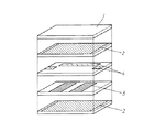
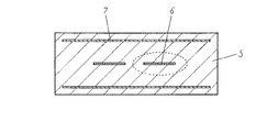
上記第1成分、第2成分および第3成分よりなる粉砕粉に、ポリビニルブチラールやアクリル樹脂等のバインダおよび可塑剤さらには有機溶剤を加えて混合・分散してセラミックスラリーとし、ドクターブレード法やダイコーティング法等によりPETフィルム等のベースフィルムの上に前記セラミックスラリーを塗布することによってセラミックグリーンシートを作製した。上記セラミックグリーンシート上にAgペーストを用いてスクリーン印刷により所望の電極パターンを印刷し、これらを所望枚数積層し、熱圧着することによって、内層もしくは表層に電極パターンを有するグリーンシート積層体を形成した。この積層体を10vol%以下の酸素含有雰囲気において、900℃〜940℃の温度で焼成することによって、焼成後の寸法が横2.5mm、縦2.0mm、厚み1mmのセラミック積層デバイスを形成した。焼成の雰囲気については、N2、Ar、CO2、O2、H2等のガスにより調節する。なお、酸素濃度についてはジルコニアセンサ等でモニタを行った。このようにして作製したセラミック積層体を断面研磨し、波長分散型X線マイクロアナライザ(WDS)の点分析によって、Si、Znの元素分析を行った。焼成前のセラミック積層体の分解斜視図を図1に、焼成後のセラミック積層体の断面図を図2に示した。ただし、外部電極等は省略している。図1は、本デバイスの積層構成の一例としてストリップライン電極3を誘電体層であるセラミックグリーンシート1で挟み、シールド電極2と入出力結合、あるいは周波数調整用のキャパシタ等を形成している内部電極4を内蔵したトリプレート型の構造を有する積層誘電体フィルタの例を示した。単独では共振器としてしか機能しないストリップライン電極を相互に電磁界結合させることでバンドパスフィルタを形成している。図2において、ストリップライン電極6は同一形状であるならば、厚みができるだけ厚い方が共振器のQ値が高くなり、フィルタとしてのロスは小さくなることが知られている。しかし、セラミック積層デバイスにおいて、内部電極の厚みを厚くすると、誘電体層との熱膨張係数の差により、誘電体素体中にクラックが生じたり、誘電体層と内部電極との間に隙間が生じたりするため、デバイス信頼性の面で不具合が生じる。素体のクラック抑制と、フィルタの電気特性とを両立させるためには、電極厚み15μm以上35μm以下であることが好ましい。
To the pulverized powder composed of the first component, the second component, and the third component, a binder such as polyvinyl butyral or acrylic resin, a plasticizer, and an organic solvent are added and mixed and dispersed to obtain a ceramic slurry. A ceramic green sheet was produced by applying the ceramic slurry on a base film such as a PET film by a coating method or the like. On the ceramic green sheet, a desired electrode pattern was printed by screen printing using Ag paste, and a desired number of these layers were laminated and thermocompression bonded to form a green sheet laminate having an electrode pattern on the inner layer or surface layer. . This laminate was fired at a temperature of 900 ° C. to 940 ° C. in an oxygen-containing atmosphere of 10 vol% or less, thereby forming a ceramic laminated device having dimensions after firing of 2.5 mm in width, 2.0 mm in length, and 1 mm in thickness. . The firing atmosphere is adjusted by a gas such as N 2 , Ar, CO 2 , O 2 , or H 2 . The oxygen concentration was monitored with a zirconia sensor or the like. The ceramic laminate thus produced was subjected to cross-sectional polishing, and elemental analysis of Si and Zn was performed by point analysis using a wavelength dispersive X-ray microanalyzer (WDS). An exploded perspective view of the ceramic laminate before firing is shown in FIG. 1, and a cross-sectional view of the ceramic laminate after firing is shown in FIG. However, external electrodes and the like are omitted. FIG. 1 shows an example in which a strip line electrode 3 is sandwiched between ceramic green sheets 1 as a dielectric layer as an example of a laminated structure of the device, and an input / output coupling with a
一方、シールド電極7は上記ストリップライン電極とは対照的にできる限り薄くすることが好ましい。シールド電極の役割としては、これにより電磁界的にフィルタ全体がシールドされているため、外部の影響等によりフィルタ特性の変化を防ぐことができるというものである。よって、上記性質上、非常に大面積を必要とする。しかしながら、この電極の厚みが厚いと、積層圧着時にセラミックグリーンシートが電極厚みを吸収できずに積層不良が生じてしまい、焼成後のデラミネーション等の原因となる場合が非常に多い。本発明によるセラミック積層デバイスにおいてはシールド電極の焼成後厚みを7μmと薄く形成した場合に、焼成後にデラミネーション等は見られず、デバイスとしての十分なシールド効果も得ることが確認できた。なお、積層時の積層性とシールド効果を両方満足するためには、電極厚みは1μm以上10μm以下であることが好ましい。 On the other hand, the shield electrode 7 is preferably as thin as possible in contrast to the stripline electrode. As a role of the shield electrode, since the entire filter is shielded electromagnetically by this, it is possible to prevent a change in filter characteristics due to an external influence or the like. Therefore, a very large area is required due to the above properties. However, if the thickness of this electrode is large, the ceramic green sheet cannot absorb the electrode thickness at the time of laminating and pressure bonding, resulting in poor lamination, which often causes delamination after firing. In the ceramic multilayer device according to the present invention, when the thickness of the shield electrode after firing was as thin as 7 μm, no delamination was observed after firing, and it was confirmed that a sufficient shielding effect as a device was obtained. In addition, in order to satisfy | fill both the lamination | stacking property at the time of lamination | stacking, and a shielding effect, it is preferable that electrode thickness is 1 micrometer or more and 10 micrometers or less.
図3には図2における電極近傍の拡大図とWDSによる分析箇所8の一例を示した。分析箇所8は電極端部より5μm以下の範囲と5μmより離れた範囲で、それぞれ5箇所測定を行った。なお、このときの測定箇所は無作為に抽出するものとし、特に電極近傍のみに偏ったり、電極より5μm離れた位置のみに偏ったりする場合においては本発明の主旨からは外れるものとする。また、焼成時の酸素濃度とWDSによる分析結果であるAg電極からの距離が5μm以下の位置におけるSi元素濃度(A)とAg電極からの距離が5μmより離れた位置におけるSi元素濃度(B)の比(A)/(B)とフィルタの損失の最小値(Top loss)を(表1)に、さらにはAg電極からの距離が5μm以下の位置におけるZn元素濃度(C)とAg電極からの距離が5μmより離れた位置におけるZn元素濃度(D)の比(C)/(D)の値とフィルタの損失の最小値(Top loss)を(表2)にそれぞれ示した。表中の(A)/(B)比、(C)/(D)比の値はそれぞれ測定箇所5点の平均値をとったものである。
FIG. 3 shows an enlarged view of the vicinity of the electrode in FIG. 2 and an example of the analysis location 8 by WDS. The analysis site 8 was measured at 5 locations each in a range of 5 μm or less from the electrode end and a range away from 5 μm. In addition, the measurement location at this time shall be extracted at random, and it deviates from the gist of the present invention particularly when it is biased only in the vicinity of the electrode or only in a

(表1)より、Ag電極からの距離が5μm以下の位置におけるSi元素濃度(A)とAg電極からの距離が5μmより離れた位置におけるSi元素濃度(B)の比(A)/(B)が2以下の場合にはフィルタのTop lossも小さく、フィルタとして良好な特性を示しているが、(A)/(B)が2より大きくなると、2以下の場合と比較してフィルタlossが約0.3dB以上低下する結果となった。また、(表2)についても同様にAg電極からの距離が5μm以下の位置におけるZn元素濃度(C)とAg電極からの距離が5μmより離れた位置におけるZn元素濃度(D)の比(C)/(D)の値が4より大きくなった場合に、4以下の場合と比較してフィルタlossは約0.3dB以上低下することが明らかになった。また、この時の酸素濃度はいずれにおいても10vol%以下であった。なお、電極近傍に偏析物が存在するような場合は、電極に近くなるほど(A)/(B)、(C)/(D)比は大きくなる傾向にある。上記同サンプルにおいて、Ag電極からの距離が2μm以下の位置におけるSi元素濃度(A)とAg電極からの距離が2μmより離れた位置におけるSi元素濃度(B)の比(A)/(B)について(表3)に、Ag電極からの距離が2μm以下の位置におけるZn元素濃度(C)とAg電極からの距離が2μmより離れた位置におけるZn元素濃度(D)の比(C)/(D)について(表4)にそれぞれ示した。 From Table 1, the ratio (A) / (B) of the Si element concentration (A) at a position where the distance from the Ag electrode is 5 μm or less and the Si element concentration (B) at a position where the distance from the Ag electrode is more than 5 μm. ) Is 2 or less, the top loss of the filter is also small, indicating good characteristics as a filter. However, when (A) / (B) is greater than 2, the filter loss is less than that of 2 or less. The result was a decrease of about 0.3 dB or more. Similarly for (Table 2), the ratio of the Zn element concentration (C) at the position where the distance from the Ag electrode is 5 μm or less to the Zn element concentration (D) at the position where the distance from the Ag electrode is more than 5 μm (C When the value of) / (D) is greater than 4, it is clear that the filter loss is reduced by about 0.3 dB or more compared to the case of 4 or less. Moreover, the oxygen concentration at this time was 10 vol% or less in any case. In the case where segregated materials exist in the vicinity of the electrode, the ratios (A) / (B) and (C) / (D) tend to increase as the distance from the electrode increases. In the sample, the ratio (A) / (B) of the Si element concentration (A) at a position where the distance from the Ag electrode is 2 μm or less and the Si element concentration (B) at a position where the distance from the Ag electrode is more than 2 μm. (Table 3), the ratio of the Zn element concentration (C) at a position where the distance from the Ag electrode is 2 μm or less to the Zn element concentration (D) at a position where the distance from the Ag electrode is more than 2 μm (C) / ( The results are shown in Table 4 for D).
(表3)、(表4)より分析範囲をより電極に近づけた場合に、(A)/(B)比が4以下となる場合や、(C)/(D)比が5以下になる場合がより好ましい。 (A) / (B) ratio becomes 4 or less, or (C) / (D) ratio becomes 5 or less when the analysis range is made closer to the electrode from (Table 3) and (Table 4). The case is more preferred.
上記より、焼成時の酸素濃度が低いと、Ag電極近傍にSiまたはZn、あるいはこれらの複合酸化物等の偏析が少なくなる。これら偏析物がAg電極近傍に偏析すると、熱膨張差によって生じるクラックやAg電極と素体の密着力低下によって生じる隙間や欠陥が生じやすい状態となる。逆に、上記偏析物の極めて少ない状態を得ることによって、Ag電極と素体との間に隙間や欠陥のない、密着性良好な界面状態が形成され、その結果として、Q値の向上、ひいてはフィルタ損失の低下につながったものと考えられる。 From the above, when the oxygen concentration at the time of firing is low, segregation of Si or Zn or a composite oxide thereof is reduced in the vicinity of the Ag electrode. When these segregated materials segregate in the vicinity of the Ag electrode, cracks caused by a difference in thermal expansion and gaps and defects caused by a decrease in adhesion between the Ag electrode and the element body are likely to occur. On the contrary, by obtaining an extremely small state of the segregated material, an interface state having good adhesion without gaps or defects is formed between the Ag electrode and the element body. As a result, the Q value is improved, and as a result This is thought to have led to a decrease in filter loss.
本発明は内部電極にAgを用い、セラミックとSiを含有するガラスとから成る誘電体磁器からなるセラミック積層デバイスにおいて、低温で焼結できるとともに、比誘電率およびQ値が高く、さらにはAgとの反応性が低く、電極近傍においてSiの偏析が少ない状況を実現することによって、高いQ値、低い損失を有するデバイスが安定して得ることができるという効果を有し、高周波領域で使用されるフィルタ等のデバイスを形成する上で非常に有用である。 The present invention uses Ag as an internal electrode, and can be sintered at a low temperature in a ceramic laminated device composed of a ceramic and glass containing Si, and has a high relative dielectric constant and Q value. By realizing a situation in which the reactivity of Si is low and the segregation of Si in the vicinity of the electrode is small, there is an effect that a device having a high Q value and a low loss can be stably obtained, and it is used in a high frequency region. It is very useful in forming devices such as filters.
1 セラミックグリーンシート
2 シールド電極
3 ストリップライン電極
4 内部電極
5 セラミック磁器
6 ストリップライン電極
7 シールド電極
8 分析箇所
DESCRIPTION OF SYMBOLS 1 Ceramic
Claims (7)
Si−アルカリ土類金属−La−O系のガラス粉末である第二成分とを混合して混合粉を得る混合工程と、A mixing step of mixing a second component that is a glass powder of Si-alkaline earth metal-La-O system to obtain a mixed powder;
前記混合粉にバインダおよび可塑剤を加えて混合、分散してセラミックスラリーを得る混合分散工程と、A mixing and dispersing step of adding a binder and a plasticizer to the mixed powder and mixing and dispersing to obtain a ceramic slurry; and
前記セラミックスラリーからなるセラミックグリーンシートを成形するシート成形工程と、A sheet forming step of forming a ceramic green sheet made of the ceramic slurry;
前記セラミックグリーンシートにAgペーストを所望のパターンで印刷するAgペースト印刷工程と、An Ag paste printing step of printing an Ag paste on the ceramic green sheet in a desired pattern;
前記セラミックグリーンシートを所望枚数積層して積層体を得る積層工程と、A lamination step of obtaining a laminate by laminating a desired number of the ceramic green sheets;
前記積層体を10vol%以下の酸素濃度で、かつ900℃以上940℃以下の温度で焼成する焼成工程とを備えたセラミック積層デバイスの製造方法。A method of manufacturing a ceramic laminated device comprising: a firing step of firing the laminate at an oxygen concentration of 10 vol% or less and at a temperature of 900 ° C. or more and 940 ° C. or less.
前記セラミック積層体が10vol%以下の酸素濃度で、かつ900℃以上940℃以下の温度で焼結されることにより、The ceramic laminate is sintered at an oxygen concentration of 10 vol% or less and at a temperature of 900 ° C. or more and 940 ° C. or less,
前記Agを含む内部電極からの距離が5μm以下の範囲におけるSi元素濃度(A)と、前記Agを含む内部電極からの距離が5μmより離れた範囲におけるSi元素濃度(B)の比である(A)/(B)が、2以下になるように構成されたことを特徴とするセラミック積層デバイス。The ratio of the Si element concentration (A) in the range where the distance from the internal electrode containing Ag is 5 μm or less to the Si element concentration (B) in the range where the distance from the internal electrode containing Ag is more than 5 μm ( A multilayer ceramic device characterized in that A) / (B) is 2 or less.
前記セラミック積層体が10vol%以下の酸素濃度で、かつ900℃以上940℃以下の温度で焼結されることにより、The ceramic laminate is sintered at an oxygen concentration of 10 vol% or less and at a temperature of 900 ° C. or more and 940 ° C. or less,
前記Agを含む内部電極からの距離が5μm以下の範囲におけるZn元素濃度(A)と、前記Agを含む内部電極からの距離が5μmより離れた範囲におけるZn元素濃度(B)の比である(A)/(B)が、4以下になるように構成されたことを特徴とするセラミック積層デバイス。The ratio of the Zn element concentration (A) in the range where the distance from the internal electrode containing Ag is 5 μm or less and the Zn element concentration (B) in the range where the distance from the internal electrode containing Ag is more than 5 μm ( A multilayer ceramic device characterized in that A) / (B) is 4 or less.
Priority Applications (5)
| Application Number | Priority Date | Filing Date | Title |
|---|---|---|---|
| JP2006070599A JP4967388B2 (en) | 2006-03-15 | 2006-03-15 | Method for manufacturing ceramic multilayer device and ceramic multilayer device |
| EP07737831A EP1986481A4 (en) | 2006-03-15 | 2007-03-06 | Ceramic laminated device and method for manufacturing same |
| PCT/JP2007/054281 WO2007119312A1 (en) | 2006-03-15 | 2007-03-06 | Ceramic laminated device and method for manufacturing same |
| US12/161,901 US7826196B2 (en) | 2006-03-15 | 2007-03-06 | Ceramic laminated device and method for manufacturing same |
| CNA200780008539XA CN101401495A (en) | 2006-03-15 | 2007-03-06 | Ceramic laminated device and method for manufacturing same |
Applications Claiming Priority (1)
| Application Number | Priority Date | Filing Date | Title |
|---|---|---|---|
| JP2006070599A JP4967388B2 (en) | 2006-03-15 | 2006-03-15 | Method for manufacturing ceramic multilayer device and ceramic multilayer device |
Publications (3)
| Publication Number | Publication Date |
|---|---|
| JP2007250728A JP2007250728A (en) | 2007-09-27 |
| JP2007250728A5 JP2007250728A5 (en) | 2009-03-26 |
| JP4967388B2 true JP4967388B2 (en) | 2012-07-04 |
Family
ID=38594717
Family Applications (1)
| Application Number | Title | Priority Date | Filing Date |
|---|---|---|---|
| JP2006070599A Expired - Fee Related JP4967388B2 (en) | 2006-03-15 | 2006-03-15 | Method for manufacturing ceramic multilayer device and ceramic multilayer device |
Country Status (5)
| Country | Link |
|---|---|
| US (1) | US7826196B2 (en) |
| EP (1) | EP1986481A4 (en) |
| JP (1) | JP4967388B2 (en) |
| CN (1) | CN101401495A (en) |
| WO (1) | WO2007119312A1 (en) |
Families Citing this family (6)
| Publication number | Priority date | Publication date | Assignee | Title |
|---|---|---|---|---|
| CN107465395A (en) * | 2014-04-03 | 2017-12-12 | 深圳振华富电子有限公司 | A kind of lamination sheet type ceramic RF low pass filter and preparation method thereof |
| JP6297914B2 (en) * | 2014-05-01 | 2018-03-20 | 日本特殊陶業株式会社 | Temperature sensor and temperature sensor |
| JP6261746B2 (en) * | 2015-01-13 | 2018-01-17 | 日本特殊陶業株式会社 | Circuit board and manufacturing method thereof |
| US20180374646A1 (en) * | 2017-06-26 | 2018-12-27 | Vishay Israel Ltd. | Wideband coupling capacitor |
| CN112408975B (en) * | 2019-08-23 | 2022-11-04 | 兴勤电子工业股份有限公司 | Ceramic composition, ceramic sintered body, multilayer ceramic electronic component and method for producing the same |
| CN113443908A (en) * | 2020-03-27 | 2021-09-28 | 兴勤电子工业股份有限公司 | Ceramic composition, ceramic sintered body and multilayer ceramic electronic component |
Family Cites Families (19)
| Publication number | Priority date | Publication date | Assignee | Title |
|---|---|---|---|---|
| JP2786977B2 (en) | 1991-09-27 | 1998-08-13 | 日本碍子株式会社 | Dielectric porcelain composition for low-temperature firing and method for producing the same |
| JP2613722B2 (en) * | 1991-09-27 | 1997-05-28 | 日本碍子株式会社 | Method for producing dielectric ceramic composition for low-temperature firing |
| JPH0855518A (en) | 1994-08-12 | 1996-02-27 | Ube Ind Ltd | Dielectric ceramic composition |
| US6165247A (en) * | 1997-02-24 | 2000-12-26 | Superior Micropowders, Llc | Methods for producing platinum powders |
| JPH11171645A (en) * | 1997-12-09 | 1999-06-29 | Hitachi Metals Ltd | Electronic part |
| JPH11189894A (en) * | 1997-12-24 | 1999-07-13 | Murata Mfg Co Ltd | Sn alloy plated film, electronic part and chip type ceramic electronic part |
| JPH11209172A (en) | 1998-01-22 | 1999-08-03 | Matsushita Electric Ind Co Ltd | Dielectric porcelain composition and composite dielectric porcelain composition |
| JP2000165048A (en) | 1998-11-26 | 2000-06-16 | Kyocera Corp | Stack circuit board and its manufacture |
| JP3917770B2 (en) * | 1999-01-22 | 2007-05-23 | 日本碍子株式会社 | Low-temperature fired porcelain and electronic component equipped with the same |
| JP3741556B2 (en) * | 1999-01-22 | 2006-02-01 | 日本碍子株式会社 | Low-temperature fired porcelain and electronic component equipped with the same |
| JP2001035741A (en) * | 1999-07-22 | 2001-02-09 | Tdk Corp | Manufacture of electronic component |
| US6876537B2 (en) * | 1999-10-07 | 2005-04-05 | Matsushita Electric Industrial Co., Ltd. | Ceramic electronic component and method for manufacturing the same |
| JP3838541B2 (en) * | 2001-03-09 | 2006-10-25 | 日本碍子株式会社 | Low-temperature fired porcelain and electronic components |
| JP2002338353A (en) * | 2001-05-17 | 2002-11-27 | Aiomu Technology:Kk | Dielectric ceramic composition |
| JP2004203646A (en) * | 2002-12-24 | 2004-07-22 | Ngk Insulators Ltd | Low temperature-fired ceramic and electronic component |
| US7230316B2 (en) * | 2002-12-27 | 2007-06-12 | Semiconductor Energy Laboratory Co., Ltd. | Semiconductor device having transferred integrated circuit |
| JP4308062B2 (en) * | 2004-03-30 | 2009-08-05 | 三洋電機株式会社 | Multilayer ceramic substrate and manufacturing method thereof |
| JP2005289701A (en) | 2004-03-31 | 2005-10-20 | Taiyo Yuden Co Ltd | Ceramic composition and ceramic wiring board using the same |
| TW200706513A (en) * | 2005-04-27 | 2007-02-16 | Murata Manufacturing Co | Dielectric ceramic, process for producing the same, and laminated ceramic capacitor |
-
2006
- 2006-03-15 JP JP2006070599A patent/JP4967388B2/en not_active Expired - Fee Related
-
2007
- 2007-03-06 US US12/161,901 patent/US7826196B2/en not_active Expired - Fee Related
- 2007-03-06 EP EP07737831A patent/EP1986481A4/en not_active Withdrawn
- 2007-03-06 CN CNA200780008539XA patent/CN101401495A/en active Pending
- 2007-03-06 WO PCT/JP2007/054281 patent/WO2007119312A1/en active Application Filing
Also Published As
| Publication number | Publication date |
|---|---|
| US7826196B2 (en) | 2010-11-02 |
| EP1986481A1 (en) | 2008-10-29 |
| CN101401495A (en) | 2009-04-01 |
| JP2007250728A (en) | 2007-09-27 |
| US20090034157A1 (en) | 2009-02-05 |
| WO2007119312A1 (en) | 2007-10-25 |
| EP1986481A4 (en) | 2012-11-28 |
Similar Documents
| Publication | Publication Date | Title |
|---|---|---|
| KR101215920B1 (en) | Ceramic multilayer substrate | |
| JP4883228B2 (en) | Low-temperature sintered ceramic sintered body and multilayer ceramic substrate | |
| JP5332807B2 (en) | Dielectric porcelain composition | |
| JP5104761B2 (en) | Ceramic substrate and manufacturing method thereof | |
| KR101290089B1 (en) | Ceramic material for low-temperature sintering, and ceramic substrate | |
| JP5321066B2 (en) | Ceramic composition and ceramic substrate | |
| JP6458863B2 (en) | Low temperature sintered ceramic materials, ceramic sintered bodies and ceramic electronic components | |
| KR20070061794A (en) | Dielectric porcelain composition and method for production thereof | |
| US10262797B2 (en) | Multilayer body and electronic component | |
| JP5533674B2 (en) | Low temperature sintered ceramic material and ceramic substrate | |
| JP4967388B2 (en) | Method for manufacturing ceramic multilayer device and ceramic multilayer device | |
| JP2007084353A (en) | Sintering aid composition for ceramic, sintering aid for ceramic, low-temperature firing ceramic composition, low-temperature fired ceramic and ceramic electronic component | |
| JP3903781B2 (en) | Composite multilayer ceramic electronic component and method for manufacturing the same | |
| JP2009096671A (en) | Dielectric ceramic and multi-layer ceramic capacitor | |
| JP2010052970A (en) | Ceramic composition, ceramic green sheet, and ceramic electronic component | |
| JP2000239061A (en) | Dielectric porcelain composition | |
| JP2005217170A (en) | Composite multilayer ceramic electronic component | |
| JP4802490B2 (en) | Electronic component, dielectric ceramic composition and method for producing the same | |
| JP2004253757A (en) | Laminated ceramic electronic part and its manufacturing method | |
| JP2006277968A (en) | Conductive paste and electronic part | |
| JP2001284818A (en) | Circuit board and its manufacturing method | |
| JP2010109133A (en) | Ceramic electronic component and electronic apparatus using the same | |
| JP2004203645A (en) | Low-temperature fired ceramic and electronic component | |
| JP2006069822A (en) | Dielectric ceramic composition and ceramic multilayer substrate |
Legal Events
| Date | Code | Title | Description |
|---|---|---|---|
| A521 | Written amendment |
Free format text: JAPANESE INTERMEDIATE CODE: A523 Effective date: 20090206 |
|
| A621 | Written request for application examination |
Free format text: JAPANESE INTERMEDIATE CODE: A621 Effective date: 20090206 |
|
| RD01 | Notification of change of attorney |
Free format text: JAPANESE INTERMEDIATE CODE: A7421 Effective date: 20091127 |
|
| A131 | Notification of reasons for refusal |
Free format text: JAPANESE INTERMEDIATE CODE: A131 Effective date: 20110621 |
|
| A521 | Written amendment |
Free format text: JAPANESE INTERMEDIATE CODE: A523 Effective date: 20110822 |
|
| TRDD | Decision of grant or rejection written | ||
| A01 | Written decision to grant a patent or to grant a registration (utility model) |
Free format text: JAPANESE INTERMEDIATE CODE: A01 Effective date: 20120306 |
|
| A01 | Written decision to grant a patent or to grant a registration (utility model) |
Free format text: JAPANESE INTERMEDIATE CODE: A01 |
|
| A61 | First payment of annual fees (during grant procedure) |
Free format text: JAPANESE INTERMEDIATE CODE: A61 Effective date: 20120319 |
|
| FPAY | Renewal fee payment (event date is renewal date of database) |
Free format text: PAYMENT UNTIL: 20150413 Year of fee payment: 3 |
|
| FPAY | Renewal fee payment (event date is renewal date of database) |
Free format text: PAYMENT UNTIL: 20150413 Year of fee payment: 3 |
|
| LAPS | Cancellation because of no payment of annual fees |