JP4959622B2 - Current sensor - Google Patents
Current sensor Download PDFInfo
- Publication number
- JP4959622B2 JP4959622B2 JP2008106715A JP2008106715A JP4959622B2 JP 4959622 B2 JP4959622 B2 JP 4959622B2 JP 2008106715 A JP2008106715 A JP 2008106715A JP 2008106715 A JP2008106715 A JP 2008106715A JP 4959622 B2 JP4959622 B2 JP 4959622B2
- Authority
- JP
- Japan
- Prior art keywords
- core
- magnetic
- magnetic body
- current sensor
- conductor
- Prior art date
- Legal status (The legal status is an assumption and is not a legal conclusion. Google has not performed a legal analysis and makes no representation as to the accuracy of the status listed.)
- Expired - Fee Related
Links
Images


Classifications
-
- H—ELECTRICITY
- H01—ELECTRIC ELEMENTS
- H01F—MAGNETS; INDUCTANCES; TRANSFORMERS; SELECTION OF MATERIALS FOR THEIR MAGNETIC PROPERTIES
- H01F3/00—Cores, Yokes, or armatures
- H01F3/10—Composite arrangements of magnetic circuits
-
- H—ELECTRICITY
- H01—ELECTRIC ELEMENTS
- H01F—MAGNETS; INDUCTANCES; TRANSFORMERS; SELECTION OF MATERIALS FOR THEIR MAGNETIC PROPERTIES
- H01F38/00—Adaptations of transformers or inductances for specific applications or functions
- H01F38/20—Instruments transformers
- H01F38/22—Instruments transformers for single phase AC
- H01F38/28—Current transformers
- H01F38/30—Constructions
-
- H—ELECTRICITY
- H01—ELECTRIC ELEMENTS
- H01F—MAGNETS; INDUCTANCES; TRANSFORMERS; SELECTION OF MATERIALS FOR THEIR MAGNETIC PROPERTIES
- H01F17/00—Fixed inductances of the signal type
- H01F17/0006—Printed inductances
- H01F17/0033—Printed inductances with the coil helically wound around a magnetic core
-
- H—ELECTRICITY
- H01—ELECTRIC ELEMENTS
- H01F—MAGNETS; INDUCTANCES; TRANSFORMERS; SELECTION OF MATERIALS FOR THEIR MAGNETIC PROPERTIES
- H01F27/00—Details of transformers or inductances, in general
- H01F27/28—Coils; Windings; Conductive connections
- H01F27/2804—Printed windings
- H01F2027/2814—Printed windings with only part of the coil or of the winding in the printed circuit board, e.g. the remaining coil or winding sections can be made of wires or sheets
-
- H—ELECTRICITY
- H01—ELECTRIC ELEMENTS
- H01F—MAGNETS; INDUCTANCES; TRANSFORMERS; SELECTION OF MATERIALS FOR THEIR MAGNETIC PROPERTIES
- H01F27/00—Details of transformers or inductances, in general
- H01F27/34—Special means for preventing or reducing unwanted electric or magnetic effects, e.g. no-load losses, reactive currents, harmonics, oscillations, leakage fields
- H01F27/346—Preventing or reducing leakage fields
-
- H—ELECTRICITY
- H01—ELECTRIC ELEMENTS
- H01F—MAGNETS; INDUCTANCES; TRANSFORMERS; SELECTION OF MATERIALS FOR THEIR MAGNETIC PROPERTIES
- H01F3/00—Cores, Yokes, or armatures
- H01F3/10—Composite arrangements of magnetic circuits
- H01F3/14—Constrictions; Gaps, e.g. air-gaps
-
- H—ELECTRICITY
- H01—ELECTRIC ELEMENTS
- H01F—MAGNETS; INDUCTANCES; TRANSFORMERS; SELECTION OF MATERIALS FOR THEIR MAGNETIC PROPERTIES
- H01F30/00—Fixed transformers not covered by group H01F19/00
- H01F30/06—Fixed transformers not covered by group H01F19/00 characterised by the structure
- H01F30/16—Toroidal transformers
Landscapes
- Engineering & Computer Science (AREA)
- Power Engineering (AREA)
- Chemical & Material Sciences (AREA)
- Composite Materials (AREA)
- Measuring Instrument Details And Bridges, And Automatic Balancing Devices (AREA)
- Transformers For Measuring Instruments (AREA)
Description
本発明は、一次導体に流れる電流を測定する電流センサに関する。 The present invention relates to a current sensor that measures a current flowing through a primary conductor.
大電流を測定する場合、該電流をそのまま電流計に流すことは危険であることから、変流器(CT)を用いて1次電流を下げて2次側に出力させることで電流を測定する電流センサが使用される。上記変流器は、交流の特性を利用したもので、コア(鉄心)に導体を巻回し形成されたコイルから2次電流を取り出す構造を有する。 When measuring a large current, it is dangerous to pass the current through the ammeter as it is, so the current is measured by lowering the primary current using a current transformer (CT) and outputting it to the secondary side. A current sensor is used. The current transformer utilizes AC characteristics and has a structure in which a secondary current is extracted from a coil formed by winding a conductor around a core (iron core).
しかしながら上記電流センサにおいても、大電流計測を行ったときには、上記コアに生じる磁束が飽和してしまい正確な電流計測が行えない場合も生じる。そこで、正確な電流計測を可能とするために、上記コア内の磁気飽和を抑制する工夫として、従来、例えばコアの断面積を大きくする、あるいは、CT出力(二次巻き線)を三次巻き線にフィードバックすることでコア内の磁束密度を小さくするという方法が提案されている(例えば特許文献1)。 However, even in the current sensor, when a large current is measured, the magnetic flux generated in the core is saturated, and an accurate current measurement may not be performed. Therefore, in order to enable accurate current measurement, conventionally, as a device for suppressing the magnetic saturation in the core, for example, the cross-sectional area of the core is increased, or the CT output (secondary winding) is tertiary winding. A method has been proposed in which the magnetic flux density in the core is reduced by feeding back to (for example, Patent Document 1).
又、リアクトルなどコア内の磁束密度の均一性が問題とならないような場合には、コア内の磁束を低減させる対策として、コアを分割し、各分割コアについてギャップを介して連結した構造を採る方法が提案されている(例えば特許文献2)。
さらにまた、磁芯に、磁性体粉末と非磁性体粉末との混成物を使用することで、磁芯の比透磁率の飽和を緩和する方法が提案されている(例えば特許文献3)。
If the uniformity of the magnetic flux density in the core is not a problem, such as a reactor, a structure in which the core is divided and connected to each divided core via a gap is taken as a measure to reduce the magnetic flux in the core. A method has been proposed (for example, Patent Document 2).
Furthermore, there has been proposed a method for relaxing saturation of the relative permeability of the magnetic core by using a composite of magnetic powder and non-magnetic powder for the magnetic core (for example, Patent Document 3).
上述したように、従来の電流センサでは、大電流計測を行う場合、コア内の磁束飽和を抑制するため、別途フィードバック回路が必要であり、装置構成が大きくなるという問題があった。又、コア内の磁束飽和を抑制する方法として、上述のようにコア断面積を大きくする方法もあるが、コア形状が大型化し、やはり小型の電流センサを構成することができないという問題がある。 As described above, the conventional current sensor has a problem in that when a large current measurement is performed, a separate feedback circuit is required to suppress magnetic flux saturation in the core, and the device configuration becomes large. Further, as a method for suppressing the magnetic flux saturation in the core, there is a method for increasing the core cross-sectional area as described above, but there is a problem that the core shape becomes large and a small current sensor cannot be formed.
さらに又、磁束飽和を抑制する対策として、上述のようにコアを分割する方法があるが、分割箇所のギャップ部分にて磁気抵抗が極端に高くなるため漏れ磁束が発生し、その結果、コア全周における磁束密度の均一性が低下する。よって、電流センサとしての測定精度が低下してしまうという問題があった。 Furthermore, as a countermeasure for suppressing the magnetic flux saturation, there is a method of dividing the core as described above. However, since the magnetic resistance becomes extremely high in the gap portion of the divided portion, a leakage magnetic flux is generated. The uniformity of the magnetic flux density in the circumference is reduced. Therefore, there is a problem that the measurement accuracy as a current sensor is lowered.
又、上記特許文献3に開示される、磁性体粉末と非磁性体粉末との混成物を磁芯に使用することで磁芯の比透磁率の飽和を緩和する方法では、磁界に対する比透磁率が変化するため、上記磁芯を電流センサへ適用すると感度が変化するという問題があった。
Further, in the method disclosed in the above-mentioned
本発明は、上述したような問題点を解決するためになされたものであり、フィードバック回路を設けることなく、測定精度を維持し、かつ従来に比べて小型のコアにて大電流計測が可能である電流センサを提供することを目的とする。 The present invention has been made to solve the above-described problems, and can maintain measurement accuracy without providing a feedback circuit, and can measure a large current with a smaller core than conventional ones. An object is to provide a current sensor.
上記目的を達成するため、本発明は以下のように構成する。
即ち、本発明の一態様における電流センサは、中央部に貫通部を有し、上記中心部を貫通して配置された一次導体を流れる一次電流にて発生した磁束を集磁するコアと、上記コアの胴部に対しトロイダル巻きされ上記コア内の磁束変化を検出する二次巻線とを有し、上記二次巻線の出力から上記一次電流を測定する電流センサにおいて、上記コアは、当該コアの周方向に当該コアを分割する磁性体にてなる複数の磁性体部と、非磁性体にてなり上記周方向に当該コアを分割する複数の非磁性体部とを有し、当該コアの全周に渡って上記磁性体部と上記非磁性体部とを交互に配置して形成され、上記二次巻線は、当該二次巻線を構成する各導体の延在方向に沿う各導体の切り口を含む上記コアにおける切り口である各コア断面が上記磁性体部及び上記非磁性体部と交差し、かつ上記コア断面における上記磁性体部の磁性体部断面積と上記非磁性体部の非磁性体部断面積との比が各コア断面で同一であるという条件下で、上記導体を上記コアの胴部に巻回してなることを特徴とする。
In order to achieve the above object, the present invention is configured as follows.
That is, a current sensor according to an aspect of the present invention includes a core that collects magnetic flux generated by a primary current that flows through a primary conductor that has a through portion at a center portion and is disposed through the center portion, and A current winding for measuring the primary current from the output of the secondary winding, wherein the core is toroidally wound around a core portion of the core and detects a change in magnetic flux in the core. A plurality of magnetic body portions made of a magnetic material dividing the core in the circumferential direction of the core and a plurality of non-magnetic body portions made of a non-magnetic material and dividing the core in the circumferential direction; The magnetic body part and the non-magnetic body part are alternately arranged over the entire circumference of the secondary winding, and the secondary winding is formed along each extending direction of each conductor constituting the secondary winding. Each core cross section which is a cut in the core including the cut of the conductor is the magnetic body portion and A condition that crosses the non-magnetic part and the ratio of the cross-sectional area of the magnetic part of the magnetic part and the non-magnetic part of the non-magnetic part in the core cross-section is the same in each core cross-section. Below, the said conductor is wound around the trunk | drum of the said core, It is characterized by the above-mentioned.
本発明の一態様における電流センサによれば、コアは、磁性体部及び非磁性体部を有し、これら磁性体部及び非磁性体部によって、当該コアの周方向に当該コアを多数に分割した。該構成によれば、非磁性体部における磁気抵抗が非常に大きいことから、コア内を通過する磁束を低減させ、コア内の磁束飽和を抑制することができる。したがって、フィードバック回路を設ける必要がなく、又、従来と同一サイズのコアにて、より大電流の計測が可能となる。逆に言えば、従来に比べて小型のコアにて大電流計測が可能である。 According to the current sensor of one aspect of the present invention, the core has a magnetic part and a nonmagnetic part, and the magnetic part and the nonmagnetic part divide the core into a large number in the circumferential direction of the core. did. According to this configuration, since the magnetic resistance in the nonmagnetic part is very large, the magnetic flux passing through the core can be reduced, and the magnetic flux saturation in the core can be suppressed. Therefore, it is not necessary to provide a feedback circuit, and a larger current can be measured with a core having the same size as the conventional one. In other words, it is possible to measure a large current with a smaller core than in the past.
一方、何の条件もなくコアを単に分割したのでは、分割断面から漏れ磁束が発生し、コア全周における磁束密度の均一性が損なわれるため、電流測定精度が低下してしまう。これに対し、上記一態様による電流センサによれば、さらに、二次巻線を構成する各導体の切り口を含む各コア断面が上記磁性体部及び上記非磁性体部と交差し、かつ上記コア断面における上記磁性体部の磁性体部断面積と上記非磁性体部の非磁性体部断面積との比が各コア断面で同一であるという条件下で、上記導体を上記コアに巻回した。よって、検出部である各導体における上記コア断面内の磁束密度を均一化することができ、コアを分割することによる測定精度の低下を抑制することができ、電流センサとしての測定精度が低下することはない。したがって、電流測定精度を維持した上で小型コアの電流センサにて大電流測定が可能となる。 On the other hand, if the core is simply divided without any condition, a leakage magnetic flux is generated from the divided cross section, and the uniformity of the magnetic flux density in the entire circumference of the core is impaired, resulting in a decrease in current measurement accuracy. On the other hand, according to the current sensor according to the above aspect, each core cross section including the cut end of each conductor constituting the secondary winding intersects the magnetic body portion and the nonmagnetic body portion, and the core The conductor was wound around the core under the condition that the ratio of the cross-sectional area of the magnetic body part in the cross section to the non-magnetic body cross-sectional area of the non-magnetic body part was the same in each core cross-section. . Therefore, the magnetic flux density in the cross section of the core in each conductor as a detection unit can be made uniform, and the decrease in measurement accuracy due to the division of the core can be suppressed, and the measurement accuracy as a current sensor is reduced. There is nothing. Therefore, it is possible to measure a large current with a small core current sensor while maintaining current measurement accuracy.
本発明の実施形態である電流センサについて、図を参照しながら以下に説明する。尚、各図において、同一又は同様の機能を有する構成部分については同じ符号を付している。又、上記電流センサは、一般的に変流器(CT)と呼ばれるものであり、中心部を貫通して配置された一次導体を流れる一次電流を測定するものである。 A current sensor according to an embodiment of the present invention will be described below with reference to the drawings. In each figure, the same reference numerals are given to components having the same or similar functions. The current sensor is generally called a current transformer (CT), and measures a primary current flowing through a primary conductor disposed through a central portion.
実施の形態1.
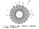
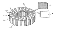
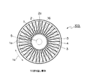
図1〜図3、図4A、及び図4Bを参照して、本発明の実施の形態1による電流センサ101について説明する。電流センサ101は、図1に示すように、コア1と、二次巻線2とを備える。
コア1は、本実施形態ではパイプを輪切りにしたような円環状にてなる胴部1a、及び中央部1bには貫通穴を有する。胴部1aは、周面1a−1と、上、下面1a−2とを有する。本実施形態では、上、下面1a−2は、それぞれ平面にてなるが、半円形等の凸形状であってもよい。上記貫通穴には、被測定電流である一次電流が流れる一次導体5が、中央部1bに沿ってつまりコア1を貫通して配置される。
The
In the present embodiment, the
さらにコア1は、当該コア1の周方向に当該コア1を分割する磁性体にてなる複数の磁性体部3と、本実施形態では磁性体部3と同一形状であり非磁性体にてなり上記周方向に当該コア1を分割する複数の非磁性体部4とを有し、当該コア1の全周に渡って磁性体部3と非磁性体部4とが交互に連結され上記全周にわたり均等に配置して形成される。尚、例えば数十から数百個の磁性体部3及び非磁性体部4にてコア1は形成される。又、本実施形態では磁性体部3と非磁性体4とは同一形状であるが、図3を参照して後述するように、磁性体部3の磁性体部断面積と非磁性体部4の非磁性体部断面積との比が各コア断面で同一であるという条件を満たす限り、同一形状に限定されるものではない。
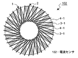
又、図1に示す電流センサ101では、磁性体部3及び非磁性体部4は、図示するように渦巻き状となるように配置している。
Furthermore, the
Further, in the
二次巻線2は、上記一次導体5によりコア1内に生じる磁束の変化を検出するもので、当該電流センサ101は、二次巻線2の出力から上記一次電流を測定する。このような二次巻線2は、コア1に対して下記の条件を満たして導体2aを、コア1の胴部1aの周囲に沿ってコア1の全周に対しトロイダル巻きしている。本実施形態では、上述した磁性体部3及び非磁性体部4の形状及び配置状態に対応して、胴部1aの上、下面1a−2において導体2aは、コア1の直径方向に沿って延在する。
The
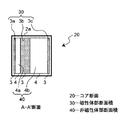
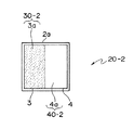
又、二次巻線2は、上記一次電流の必要な検出精度を確保するために、コア1の全周にわたり均一に巻き回される必要がある。即ち、二次巻線2を構成する各導体2aの延在方向に沿う各導体2aの切り口を含むコア1における切り口、つまり図1に示す例えばA−A’線におけるコア1の断面である図3に示す各コア断面20に着目する。各導体2aに対応するそれぞれのコア断面20は、磁性体部3及び非磁性体部4と交差し、かつコア断面20における磁性体部3の磁性体部断面積と非磁性体部4の非磁性体部断面積との比が各コア断面20で同一であるという条件を満足するように、導体2aがコア1に巻回され、二次巻線2が形成される。ここで、例えば図3に示されるコア断面20の場合、上記磁性体部断面積は、磁性体部3の断面積3a、3b、3cを加えた断面積30であり、上記非磁性体部断面積は、非磁性体部4の断面積4a、4bを加えた断面積40である。各導体2aにおけるそれぞれのコア断面20において、コア断面20にて切断される磁性体部3及び非磁性体部4の断面形状は異なるが、上記磁性体部断面積30と上記非磁性体部断面積40との比率が同一となるように、導体2aと磁性体部3及び非磁性体部4とを相対的に配置、具体的には、導体2aと、磁性体部3及び非磁性体部4の形状並びに配置と、を調整する。
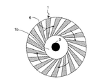
Further, the
上述の条件を満たすように、導体2aと磁性体部3及び非磁性体部4とを相対的に配置することで、以下のような効果が得られる。即ち、図4Aに示すように、コア1を貫通する一次導体5に電流が流れた場合、この一次導体5の周方向に、電流に応じた磁束6が発生する。このとき上述のようなコア1を適用した場合、図4Bに示すように、透磁率の高い磁性体部3には周辺より磁束6が集磁され、逆に非磁性体部4であるスペーサ部分では、周辺の空気と透磁率が近いため磁束6が拡散する。そのためコア1内の磁束6の密度に粗密が生じる。
しかし、上述の条件を満足させることで、それぞれのコア断面20内を通過する磁束密度の和が等しくなり、電磁誘導によって発生する起電力が均一化される。このため、電流センサ101における一次電流の検出精度の低下を抑制することができる。
By arranging the
However, by satisfying the above-mentioned conditions, the sum of the magnetic flux density passing through each
又、磁性体部3と非磁性体部4とによりコア1を形成したことから、非磁性体部4における磁気抵抗が非常に大きく、コア1内を通過する磁束を低減し、コア1内の磁束飽和を抑制することができる。したがって、フィードバック回路を設ける必要がなく、又、従来と同一サイズのコアにて、より大電流の計測が可能となる。
Further, since the
又、一般に空芯電流センサ(ロゴスキーコイルなど)と言われるものと比較すると、本実施形態の電流センサ101では、透磁率の高い磁性体部3が、二次巻線2の内側に存在するため、電流センサ101は高感度となる。
又、一般に鉄心電流センサと言われる、磁性材料のみにてコアを形成したものと比較すると、本実施形態の電流センサ101では、透磁率の低い非磁性体部4がコア1に存在するため、コア1の磁気飽和が抑制され、測定レンジを広域化することができる。
Compared with what is generally called an air-core current sensor (Rogowski coil or the like), in the
In addition, compared with a core sensor formed by using only a magnetic material, which is generally referred to as an iron core current sensor, in the
さらに又、本実施形態の電流センサ101では、コア1の磁気飽和を抑制できることから、従来の電流センサにおける磁気飽和対策、つまりコアサイズの大型化、を図る必要がなく、電流センサのサイズを大幅に小型化することができる。
又、上述したように、本実施形態の電流センサ101では、透磁率の高い磁性体部3と透磁率が低い非磁性体部4との両方を配置することで、コア1内の磁気抵抗を任意にコントロールすることができ、測定する一次電流に応じた感度に電流センサを調整することが可能である。
Furthermore, in the
Further, as described above, in the
又、上述したようなコア断面20における条件を満足する限り、磁性体部3及び非磁性体部4の形状及び配置、並びに導体2aの巻き方は、例えば図1に示す形態に限定されるものではなく、例えば以下のような変形例を採ることができる。
例えば図5に示す電流センサ102のように、磁性体部3−1及び非磁性体部4−1は放射状形状としてそれぞれコア1の直径方向に沿うように配置し、かつ胴部1aの上、下面1a−2にて導体2aは渦巻き状に配置してもよい。図5に示す形態では、磁性体部3−1及び非磁性体部4−1の形状が、図1に示す形態における磁性体部3及び非磁性体部4に比べて単純であり、コア1の作製が容易になるという利点がある。
Moreover, as long as the conditions in the
For example, like the
又、図6に示す電流センサ103のように、磁性体部3−2及び非磁性体部4−2は螺旋形状とし、かつ胴部1aの上、下面1a−2にて導体2aはコア1の直径方向に沿って延在するように配置してもよい。図6に示す形態では、図5に示す形態に比べて磁性体部3−2及び非磁性体部4−2の形状が複雑となるが、二次巻線2の導体2aは直径方向に沿って延在させればよく導体2aの巻回が容易であるという利点がある。
Further, like the
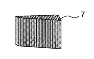
又、磁性体部3、3−1、3−2において、一般的な電流センサのコア製作と同様に、渦電流対策として、図7に示すように、表面が電気的に絶縁された磁性体箔を積層して、コアの直径方向にコアを分割し、電気絶縁された磁性体部7を製作しても良い。尚、図7では、電流センサ101に使用される磁性体部7を示している。
Further, in the
又、図8に示す電流センサ104のように、磁性体部3−3、非磁性体部4−3、及び導体2aの配置は、図1に示す電流センサ101の場合と同様であるが、コア断面20における磁性体部3−3及び非磁性体部4−3を、コア1の軸方向1cに対して傾斜して配置してもよい。
Further, like the
さらに又、図9に示すように、折り返し導体16を有する電流センサ105を構成することもできる。折り返し導体16は、コア1の胴部1aの全周に対してトロイダル巻きされた二次巻線2の導体2aを折り返して形成された導体部分であり、胴部1aに巻回された二次巻線2の一次導体5に対する傾きの影響を相殺する方向に沿って胴部1aに設けられる。図9に示す例では、折り返し導体16は、トロイダル巻きされた二次巻線2の導体2aに接続した状態で導体2aを折り返し、コア1の周方向1dに沿って胴部1aの周面1a−1に対向するように一周分、延在する。折り返し導体16を形成する上記一周分の導体の長さは、胴部1aにトロイダル巻きされた二次巻線2の導体2aの全長に対応する。尚、折り返し導体16と、胴部1aにトロイダル巻きされた導体2aとは、電気的に絶縁された状態である。
Furthermore, as shown in FIG. 9, a
図9に示す折り返し導体16の形態は一例であり、上述のようにトロイダル巻きされた二次巻線2の全長に相当する長さにて折り返し導体16を設ければ良く、例えば、胴部1aにトロイダル巻きした導体2aを折り返し、逆方向に胴部1aにトロイダル巻きして、折り返し導体16を形成することもできる。
The form of the folded
上述のように折り返し導体16を設けることで、コア1に対する一次導体5の傾きが二次巻線2に与える影響をキャンセルすることができる。
By providing the folded
実施の形態2.
次に、図10を参照して本発明の実施の形態2における電流センサ106について説明する。尚、図10では、電流センサ106を構成するコア部分のみを図示し、二次巻線2の図示は、省略している。
上述した実施の形態1では、コア1は、磁性体部3及び非磁性体部4を一体的に形成した一つの構造体から構成されている。これに対し本実施の形態2の電流センサ106では、コア1は、複数、ここでは2つの分割コア21、22から形成されている。この点で実施の形態1と実施の形態2とは異なる。複数の分割コアを組み合わせて一つのコア1を形成することで、電流センサ特性として、任意の感度係数の分布を得ることが可能となる。
電流センサ106のその他の構成及び変形例については、実施の形態1において上述した説明が適用可能であるので、ここでのそれらの説明は省略する。
Next, the
In the first embodiment described above, the
About the other structure and modification of the
分割コア21、22について、さらに詳しく説明する。
実施の形態1に記載したコア1では、磁性体部3と非磁性体部4とは同一形状でありコア1の全周にわたりそれらを交互に均等に配置することで、電流センサの感度を制御している。又、非磁性体部4は、上述のように非磁性材料にてなり、磁性体部3と磁性体部3との間にギャップ領域を設けることを目的として使用されている。本実施の形態2では、互いに感度特性の異なる、複数の分割コアを製作し、これらを一つにまとめ、まとめたものに二次巻線2を巻回することで、任意のセンサ特性を得るものである。
The
In the
分割コア21,22は、本実施形態ではともに円環状で同形状であり、互いを厚み方向に重ね合わされることで一つのコアを形成する。尚、分割コア21,22から形成されるコアを、コア23とする。
分割コア21は、図10の(a)に示すように、比較的感度が低くなるように、全周における磁性体部3の領域の割合を小さく設計した低感度設定用磁性体部3−4と、低感度設定用非磁性体部4−4とを、分割コア21の周方向に沿って交互に配置した。
分割コア22は、図10の(b)に示すように、比較的感度が高くなるように、全周における磁性体部3の割合を大きく設計した高感度設定用磁性体部3−5と、高感度設定用非磁性体部4−5とを、分割コア22の周方向に沿って交互に配置した。
The
As shown in FIG. 10A, the
As shown in FIG. 10B, the
よってコア23は、比較的低感度の分割コア21と、比較的高感度の分割コア22とを厚み方向に重ね合わせて構成され、これらに対し一括して二次巻線2を巻回する。つまり、それぞれの分割コア21,22では、磁性体部と非磁性体部との割合を異ならせており、分割コア毎に磁束密度は変化する。このような各分割コアをまとめて形成したコアに対して二次巻線を巻回する構成により、センサ特性として一次電流に応じ多段階に変化する感度係数の分布を持つ電流センサを構成することができ、電流センサの感度曲線を自在に設定することが可能となる。
Therefore, the
ここで、図3を参照して上述したコア断面20を引用して、分割コア21及び分割コア22のそれぞれの上記コア断面20における上記磁性体部断面積30と上記非磁性体部断面積40との比が、それぞれの分割コア21,22において異なっていることを説明する。
即ち、図10の(a)に示したA−A’部は、分割コア21において二次巻線2の導体2aが位置する一箇所に対応し、図11Aに示すように、A−A’部における分割コア21のコア断面20をコア断面20−1とする。又、コア断面20−1における上記磁性体部断面積30を磁性体部断面積30−1とし、上記非磁性体部断面積40を非磁性体部断面積40−1とする。同様に、図10の(b)に示したB−B’部は、分割コア22において二次巻線2の導体2aが位置する一箇所に対応し、図11Bに示すように、B−B’部における分割コア22のコア断面20をコア断面20−2とする。又、コア断面20−2における上記磁性体部断面積30を磁性体部断面積30−2とし、上記非磁性体部断面積40を非磁性体部断面積40−2とする。
Here, referring to the
That is, the AA ′ portion shown in FIG. 10A corresponds to one place where the
図11Aと図11Bとを見比べると、分割コア21のコア断面20−1における磁性体部断面積30−1と非磁性体部断面積40−1との比は、分割コア22のコア断面20−2における磁性体部断面積30−2と非磁性体部断面積40−2との比と異なっていることが判る。
Comparing FIG. 11A and FIG. 11B, the ratio of the magnetic body section area 30-1 and the nonmagnetic body section area 40-1 in the core section 20-1 of the
尚、図3を参照して上述したように、分割コア21において、巻回された各導体2aに対応するそれぞれのコア断面20−1における磁性体部断面積30−1と非磁性体部断面積40−1との比は、同一となっている。同様に、分割コア22において、巻回された各導体2aに対応するそれぞれのコア断面20−2における磁性体部断面積30−2と非磁性体部断面積40−2との比は、同一となっている。
As described above with reference to FIG. 3, in the divided
以上のようにして形成されるコア23のセンサ特性グラフを図12に示す。
感度を高く設定した分割コア22では、一次導体5を流れる一次電流に対する感度が高く設定されている分、磁気飽和の傾向が顕在化する一次電流は、感度を低く設定した分割コア21に比較して小さく、磁気飽和の影響が顕在化する一次電流値以上では、感度係数が小さくなる。結果として、分割コア22は、一次電流に対するセンサ出力の変化が小さくなる高感度設定用磁性体部のみの出力特性29のような特性を示す。
FIG. 12 shows a sensor characteristic graph of the core 23 formed as described above.
In the
一方、感度を低く設定した分割コア21では、一次電流に対する感度が低く設定されている分、磁気飽和の傾向が顕在化する一次電流は、感度を高く設定した分割コア22に比較して大きい。そのため、分割コア21は、低感度設定用磁性体部のみの出力特性28の様な特性を示す。しかしながら、一次導体5を流れる一次電流がより大きくなると、感度を低く設定した分割コア21でも、感度を高く設定した分割コア22と同様に飽和傾向を示す。
On the other hand, in the
このように異なる感度の分割コア21,22を一つにまとめた分割コア23は、低感度設定用磁性体部のみの出力特性28と、高感度設定用磁性体部のみの出力特性29とを重ね合わせた合成出力特性30の様なセンサ特性を示す。
尚、本実施の形態2では、感度の異なる分割コア21,22の2つを一つのコア23にまとめた事例を記載しているが、必要に応じて3個以上の分割コアを用いても、同様に設計することが可能である。
又、分割コアの一例として、非磁性体部を有しない磁性体部のみからなるものも、最も高感度化した分割コアとして、同様にセンサ特性の設計に適用可能である。
The
In the second embodiment, an example in which two divided
Further, as an example of a split core, a split core having only a magnetic part that does not have a non-magnetic part can be similarly applied to the design of sensor characteristics as a split core with the highest sensitivity.
以上説明したように、感度の異なる複数の分割コアをまとめて一つのコア23を構成して電流センサを作製することで、用途に応じた感度係数分布を持つセンサ特性を設計可能となる。
As described above, a plurality of divided cores having different sensitivities are combined to form one
又、上述の実施形態2では、分割コア21,22の厚み方向に分割コア21,22を積み重ねているが、各分割コアの組み合わせ方は、これに限定されない。例えば、図13に示すように、それぞれの分割コアにおける内径及び外径を調整することで、入れ子状の分割コア41,42を形成し、これらを合体させてコア43を構成しても良い。尚、3−6、3−7は磁性体部を示し、4−6、4−7は非磁性体部を示す。この形態では、組み合わされて形成されるコアの厚みを薄くできるという効果がある。又、図13では、2つの分割コア41,42を合体させた場合であるが、さらに、3個以上の入れ子状の分割コアを合体させて一つのコアを形成してもよい。
In the second embodiment, the
又、上述の実施形態2では、別々に製作した分割コアを合体させているが、切削等により一つのコアに、非磁性体部を形成する種々の領域を形成し、感度係数を調整しても同等の効果が得られる。
In
上述したように、複数の分割コアから一つのコアを形成した場合におけるセンサ特性が有効である事例として、次のものがある。例えば、定格値以下の電流領域については高精度(高分解能)計測を行い、定格値を超える電流領域については分解能を落とし、傾向のみを測定する場合などが相当する。このような事例では、高精度測定を行いたい電流領域を計測器の測定レンジ(A/Dレンジ)の大部分に割り付けることが可能となる。 As described above, there are the following cases where the sensor characteristics are effective when one core is formed from a plurality of divided cores. For example, the current region below the rated value is measured with high accuracy (high resolution), the current region exceeding the rated value is reduced in resolution, and only the tendency is measured. In such a case, it is possible to allocate the current region where high-precision measurement is desired to most of the measurement range (A / D range) of the measuring instrument.
実施の形態3.
次に、本発明の実施の形態3による電流センサについて、図14及び図15を参照して説明する。本実施の形態は、上述の実施の形態1、2にて説明した電流センサを、形状制御性に優れたメッキもしくはプリント基板にて製作したものである。
Next, a current sensor according to
図14及び図15に示す本実施形態の電流センサ107は、図1に示す電流センサ101の形態を基板にて作製したものである。勿論、上述した電流センサ102〜106の形態を、以下に説明する構成にて作製してもよい。
電流センサ107は、第1巻線パターン基板9−1及び第2巻線パターン基板9−2と、これらの巻線パターン基板9−1、9−2に挟まれるコアパターン基板12とを備える。第1巻線パターン基板9−1は、例えばプリント基板等の非磁性体にてなる基板上に、コア1の上、下面1a−2を延在する上記導体2aに対応する導体部分であって導電材料にてなる第1導体8aを、本例では放射状に、パターン形成した基板である。よって、第1導体8aは、図示するように、上記上、下面1a−2を模したドーナツ状の領域内に、該ドーナツ形状の直径方向に沿って形成されている。第2巻線パターン基板9−2についても、第1巻線パターン基板9−1と同様に作製される。尚、導電材料にて基板上に放射状にパターン形成された導体を、第2導体8bとする。
A
The
コアパターン基板12は、非磁性体にてなる基板であり、上述のコア1の上、下面1a−2における磁性体部3及び非磁性体部4の配置構成を基板面に形成したもので、詳細後述する例えばメッキによって、コア1の磁性体部3に対応して、例えば電解メッキにより磁性体パターン11を渦巻き状にコアパターンを形成した基板である。よって、コアパターン基板12の表面上には、上記磁性体にてなる磁性体パターン11と、コアパターン基板12の表面にてなる非磁性体にてなる非磁性体部14とが交互に配置されることになる。即ち、後述するように、コアパターン基板12の表面に形成した磁性体パターン11は、薄膜ながらも厚みを有することから、これらの磁性体パターン11に挟まれた非磁性体部14に対応して凹部が形成されることになる。よって、下記するように、当該コアパターン基板12が巻線パターン基板9−1、9−2に挟まれることで、非磁性体部14に対応して形成される上記凹部の空間に、接着剤等の非磁性材が充填されること、あるいは空気領域が残存することで非磁性体部14を形成することになる。又、コアパターン基板12に溝を掘り該溝に磁性体を設け、磁性体パターンを形成することもできる。
The
上述のように形成された第1巻線パターン基板9−1、第2巻線パターン基板9−2、及びコアパターン基板12は、基板の厚み方向において第1導体8aと第2導体8bとの配置を一致させた状態にて、コアパターン基板12を間に配して第1巻線パターン基板9−1及び第2巻線パターン基板9−2にて挟み、貼り合わせる。その後、第1導体8a、第2導体8b、及び磁性体パターン11の中心部に、第1巻線パターン基板9−1、第2巻線パターン基板9−2、及びコアパターン基板12を貫通し、一次導体5を配置するための貫通穴13を形成する。さらに、それぞれの第1導体8aにおける両端部分には、対応する第2導体8bの両端部分と連通させて、第1巻線パターン基板9−1、第2巻線パターン基板9−2、及びコアパターン基板12を貫通してスルーホールが形成される。それぞれのスルーホールには、第1導体8aと第2導体8bとを電気的に接続する接続導体10がメッキ、導電性材料の充填、等の方法にて形成される。
The first winding pattern substrate 9-1, the second winding pattern substrate 9-2, and the
上述したように構成される電流センサ107では、第1導体8a、接続導体10、及び第2導体8bにて二次巻線2が形成され、磁性体パターン11及び非磁性体部14にてコア1が形成されることになる。
このような電流センサ107においても、上述した電流センサ101が奏する効果と同様の効果を得ることができる。
In the
Also in such a
又、電流センサ107によれば、コアを、プリント基板やメッキ等の形状制御性に優れた手法にて製作することで、コア1における磁性体パターン11の幅(コア幅)や、非磁性体部14の幅であるギャップ間距離等の製作精度を高めることができ、よって電流センサとしての測定精度を向上させることができる。さらにまた、コア1を、プリント基板やメッキ等の形状制御性に優れた手法にて製作することで、磁性体パターン11及び非磁性体部14を配置したコアを容易に作製することができる。
Further, according to the
又、本実施の形態3では、コアパターン基板12は一枚だけであるが、複数枚のコアパターン基板12を積層してコア1を形成することも可能である。この場合、各コアパターン基板12における磁性体パターン11の形成精度は、電流センサの測定精度に影響する。電流センサ107では、上述のように磁性体パターン11を高い形成精度にて作製可能なことから、当該電流センサ107は、高い測定精度を達成することが可能となる。
In the third embodiment, only one
又、第1導体8a及び第2導体8bを、形状制御性に優れた手法にて製作することで、第1導体8a及び第2導体8bの位置(角度等)等の製作精度を高めることができる。
又、多層基板を用い、第1導体8a及び第2導体8bにて二次巻線、及び、磁性体パターン11及び非磁性体部14にて多数分割コアを、それぞれ一括して製作することで、電流センサの小型化及び低コスト化を図ることが可能となる。
In addition, by manufacturing the
Also, by using a multi-layer substrate, a secondary winding with the
上述した手法では、磁性体パターン11の厚みは、精々百μm程度と非常に薄く、よってコア断面積は小さい。しかしながら、例えばコア材、つまり磁性体パターン11の材料としてパーマロイ等を使用すると、該材料は、周辺の空気と比較して透磁率が3桁以上高いため、形成された電流センサ107におけるコア断面20を通過する磁束6の平均密度は、空心コイルと比較して数倍程度、高くなる。よって、磁性体パターン11について適切な材料を選択することで、電流センサの感度を高感度に設定可能である。
In the above-described method, the thickness of the
又、上述のように複数枚のコアパターン基板12を積層した場合には、さらに高感度化を図ることができる。
又、本実施の形態3では、第1巻線パターン基板9−1、第2巻線パターン基板9−2、及びコアパターン基板12を貼り合わせた後、貫通穴13を開けたが、勿論、貫通穴13を設けた各基板を貼り合わせても良い。
又、第1導体8a、第2導体8b、磁性体パターン11のパターン部分に対して、第1巻線パターン基板9−1、第2巻線パターン基板9−2、及びコアパターン基板12のサイズが大きい場合には、上記パターン部分以外の、基板の不要な部分を除去してもよい。
In addition, when a plurality of
In the third embodiment, after the first winding pattern substrate 9-1, the second winding pattern substrate 9-2, and the
Also, the size of the first winding pattern substrate 9-1, the second winding pattern substrate 9-2, and the
コアパターン基板12に電解メッキにて磁性体パターン11を形成する場合、まず通常のプリント基板技術にて、パターン形状及び引き出し線をコアパターン基板12に形成する。このコアパターン基板12を金属イオンが溶融しているメッキ液に漬け込み、電極に電圧を印可することで、上記パターン形状に応じた強磁性体膜の磁性体パターン11が形成される。パターン形状は、一般的なプリント基板技術により形成されるため、寸法等が高精度にて形成可能である。このようなパターン形状の電極上にメッキされるため、磁性体パターン11の形状も高精度に形成可能である。
When the
但し、電解メッキの場合、図16に示すように、コアパターン基板12に対応する、電解メッキ直後のコアパターン基板12−1では、磁性体パターン11を形成するための電極パターン11’は、全て結線されている必要がある。そのため、メッキ直後の磁性体パターン11’は、連結部分14により結線された状態となる。よって磁性体パターン11のみを形成するためには、連結部分14を除去する必要がある。この除去方法としては、コアパターン基板12から不要部分として除去される除去部分18に連結部分14を形成する、あるいは、一次導体5を貫通させるため貫通穴13として除去される除去部分19に連結部分14を形成する等がある。このような方法によれば、連結部分14のみを単独で除去する工程を省くことができる。
However, in the case of electrolytic plating, as shown in FIG. 16, in the core pattern substrate 12-1 corresponding to the
又、連結部分14を除去しても、磁性体パターン11には、電極用の引き出し線15が残るが、二次巻線2を構成する第1導体8aを連結するスルーホール位置20の外側に位置すれば、問題はない。又、内側に位置する場合であっても、引き出し線15が第1導体8aと略平行であれば、影響は小さく、図17に示すように、必ずしも除去する必要はない。
Even if the connecting
実施の形態4.
ここでは、上述した実施の形態1における電流センサ101を例に、図18から図21を参照して当該電流センサ101の製造方法の幾つかの例を以下に説明する。
実施の形態1における電流センサ101では、磁性体部3は、非磁性体部4によって完全に分離されている。そのため磁性体部3同士の位置関係を保ち、コア1を形成することは容易ではない。そこで、つながっていても問題のない非磁性体部4を連結したような形状にてなり非磁性体部4を兼用する、図18に示すコア保持ケース31を製作する。よって、該コア保持ケース31は、磁性体部3に対応した形状にてなる嵌合部32を有する。そして嵌合部32に、別途製作した磁性体部3を挿入することで、コア1を作製する。
尚、磁性体部3は、嵌合部32に嵌合可能な形状に製作すれば良く、その製作方法は、プレス、焼結等、特に問わない。
Here, taking the
In the
The
又、図19に示すように、磁性体部3に相当する磁性体部34と、非磁性体部4に相当する非磁性体部35とを、半円形でパイプ状の収納ケース33に、交互に装填する方法を採ることもできる。磁性体部34及び非磁性体部35を装填した半円形状の収納ケース33を2つ繋ぎ合わせてコア1を作製し、それに二次巻線2を施すことで、電流センサ101を作製する。
尚、磁性体部34及び非磁性体部35のそれぞれの厚み等は、電流センサの所望の感度に応じて決定される。又、感度調整のため、1個の磁性体部34、及び1個の非磁性体部35の厚みが大きくなり、収納ケース33への装填が困難になる場合等には、薄い磁性体部34及び非磁性体部35を積層することで、1個の磁性体部34、及び1個の非磁性体部35を作製することもできる。
Further, as shown in FIG. 19, a
In addition, each thickness etc. of the
又、図20に示すような方法を採ることもできる。即ち、磁性体材料にて形成され、複数の磁性体部3を連結部36aにより連結した直線状のコア形成用部材36を作製する。次に、このコア形成用部材36の両端部に位置する磁性体部3と連結部36aとを連結するように、直線状のコア形成用部材36を円環状に変形させ、コア1の基礎となるコア基礎部材37を形成する。
次に、図21に示すように、コア基礎部材37を金型38へ装填し、金型38内へ非磁性材料を充填し、コア基礎部材37をモールドする。このモールド工程により、各磁性体部3の間には、非磁性体部4が形成されるとともに、磁性体部3及び非磁性体部4は一体化される。
Also, a method as shown in FIG. 20 can be adopted. That is, the linear
Next, as shown in FIG. 21, the
尚、上述のモールドによる手法を採らず、上述した実施の形態2にて説明した分割コアの手法にてコアを形成することも可能である。即ち、コア基礎部材37が嵌合可能であり、かつ、非磁性材料にて作製され非磁性体部4を形成する非磁性体部用部材を用意し、該非磁性体部用部材と、コア基礎部材37とを合体させることで、上述のモールドした状態と同じ物を得ることができる。
In addition, it is also possible to form a core by the method of the split core demonstrated in
次に、一体化された磁性体部3及び非磁性体部4に対して、図21に示すように、コア基礎部材37に備わる連結部36aを切削加工等により除去する。これにより、コア1が形成される。
以上の製造方法により、完全に分離されている磁性体部3の位置決め及び固定の両方の動作を容易に達成することができる。
Next, as shown in FIG. 21, with respect to the integrated
By the above manufacturing method, both the positioning and fixing operations of the
尚、上述の説明では、コア基礎部材37は、円形状に成形したが、用途に応じて矩形形状等に成形してもかまわない。これは、上述の説明で用いた実施の形態1の場合に限らず、実施の形態2、3にて説明したコアについても、その形状は円形に限定するものではない。
又、上述の説明では、磁性材料から形成され複数の磁性体部3を形成したコア形成用部材36を用いたが、非磁性材料にてなり直線状で複数の非磁性体部4を形成した非磁性体部形成用部材を作製し、使用することもできる。但し、この場合、例えば円環状に上記非磁性体部形成用部材を変形した後、磁性部材にてモールドすることは、上記非磁性体部形成用部材の耐熱温度上、困難又は不可能な場合がある。よって、図18を参照して説明したような、予め、上記非磁性体部形成用部材に嵌合可能な磁性体部3を作製しておき、該磁性体部3を上記非磁性体部形成用部材に嵌合するという手法を採ることになる。
In the above description, the
In the above description, the
1…コア、2…二次巻線、2a…導体、3…磁性体部、4…非磁性体部、
5…一次導体、6…磁束、7…磁性体部、8a…第1導体、8b…第2導体、
9−1…第1巻線パターン基板、9−2…第2巻線パターン基板、10…接続導体、
11…磁性体パターン、12、12−1…コアパターン基板、13…貫通穴、
16…折り返し導体、20…コア断面、21,22…分割コア、23…コア、
30…磁性体部断面積、32…嵌合部、36…コア形成用部材、
40…非磁性体部断面積、41,42…分割コア、43…コア、
101〜107…電流センサ。
DESCRIPTION OF
5 ... Primary conductor, 6 ... Magnetic flux, 7 ... Magnetic body part, 8a ... First conductor, 8b ... Second conductor,
9-1 ... 1st winding pattern board, 9-2 ... 2nd winding pattern board, 10 ... Connection conductor,
DESCRIPTION OF
16 ... folded conductor, 20 ... core cross section, 21, 22 ... split core, 23 ... core,
30 ... Cross-sectional area of magnetic body part, 32 ... Fitting part, 36 ... Member for core formation,
40 ... non-magnetic body cross-sectional area, 41, 42 ... split core, 43 ... core,
101-107 ... Current sensors.
Claims (10)
上記コアは、当該コアの周方向に当該コアを分割する磁性体にてなる複数の磁性体部と、非磁性体にてなり上記周方向に当該コアを分割する複数の非磁性体部とを有し、当該コアの全周に渡って上記磁性体部と上記非磁性体部とを交互に配置して形成され、
上記二次巻線は、当該二次巻線を構成する各導体の延在方向に沿う各導体の切り口を含む上記コアにおける切り口である各コア断面が上記磁性体部及び上記非磁性体部と交差し、かつ上記コア断面における上記磁性体部の磁性体部断面積と上記非磁性体部の非磁性体部断面積との比が各コア断面で同一であるという条件下で、上記導体を上記コアの胴部に巻回してなる、
ことを特徴とする電流センサ。 A core having a through-hole at the center and collecting magnetic flux generated by a primary current flowing through a primary conductor disposed through the center; and toroidally wound around the core of the core A current sensor for measuring the primary current from the output of the secondary winding.
The core includes a plurality of magnetic body portions made of a magnetic body that divides the core in the circumferential direction of the core, and a plurality of non-magnetic body portions made of a non-magnetic body that divides the core in the circumferential direction. Having the magnetic body part and the non-magnetic body part alternately arranged over the entire circumference of the core,
In the secondary winding, each core cross section which is a cut in the core including cuts of the respective conductors along the extending direction of the respective conductors constituting the secondary winding includes the magnetic body part and the non-magnetic body part. The conductors are crossed under the condition that the ratio of the cross-sectional area of the magnetic body section of the magnetic body section to the non-magnetic body section of the non-magnetic body section is the same in each core cross-section. Wound around the core of the core,
A current sensor characterized by that.
Priority Applications (4)
| Application Number | Priority Date | Filing Date | Title |
|---|---|---|---|
| JP2008106715A JP4959622B2 (en) | 2008-04-16 | 2008-04-16 | Current sensor |
| US12/255,783 US7633287B2 (en) | 2008-04-16 | 2008-10-22 | Current sensor |
| CN2008101787625A CN101562073B (en) | 2008-04-16 | 2008-11-26 | Current sensor |
| HK10101633.9A HK1135230B (en) | 2008-04-16 | 2010-02-12 | Current sensor |
Applications Claiming Priority (1)
| Application Number | Priority Date | Filing Date | Title |
|---|---|---|---|
| JP2008106715A JP4959622B2 (en) | 2008-04-16 | 2008-04-16 | Current sensor |
Publications (3)
| Publication Number | Publication Date |
|---|---|
| JP2009260006A JP2009260006A (en) | 2009-11-05 |
| JP2009260006A5 JP2009260006A5 (en) | 2010-11-18 |
| JP4959622B2 true JP4959622B2 (en) | 2012-06-27 |
Family
ID=41200593
Family Applications (1)
| Application Number | Title | Priority Date | Filing Date |
|---|---|---|---|
| JP2008106715A Expired - Fee Related JP4959622B2 (en) | 2008-04-16 | 2008-04-16 | Current sensor |
Country Status (3)
| Country | Link |
|---|---|
| US (1) | US7633287B2 (en) |
| JP (1) | JP4959622B2 (en) |
| CN (1) | CN101562073B (en) |
Cited By (1)
| Publication number | Priority date | Publication date | Assignee | Title |
|---|---|---|---|---|
| KR101818924B1 (en) * | 2016-12-08 | 2018-01-17 | 주식회사 코본테크 | Voltage and current Sensing device type Fluxgate with PCB multi-layer core structure |
Families Citing this family (17)
| Publication number | Priority date | Publication date | Assignee | Title |
|---|---|---|---|---|
| JP5414420B2 (en) * | 2009-08-21 | 2014-02-12 | ジェコー株式会社 | Current sensor and manufacturing method thereof |
| KR101169301B1 (en) | 2011-03-04 | 2012-07-30 | 주식회사 셀픽 | Current sensor using rogowski coil |
| CN107076784B (en) * | 2014-12-15 | 2019-06-14 | 株式会社村田制作所 | current sensor |
| JP6506573B2 (en) * | 2015-03-10 | 2019-04-24 | 株式会社トーキン | Coil parts |
| JP6790405B2 (en) * | 2016-03-25 | 2020-11-25 | 中国電力株式会社 | Current detection sensor and ground fault point positioning system |
| KR101747075B1 (en) | 2017-01-18 | 2017-06-16 | 주식회사 코본테크 | Built-in control power supply CT device with PCB multi-layer core structure |
| KR101747076B1 (en) | 2017-01-20 | 2017-06-16 | 주식회사 코본테크 | Integrated composite current sensor of CT and ZCT using PCB multi-layer core structure |
| JP7003421B2 (en) * | 2017-03-07 | 2022-01-20 | 株式会社明電舎 | Winding equipment for pulse power supply |
| GB2562279B (en) * | 2017-05-10 | 2020-04-29 | Megger Instruments Ltd | Current sensor |
| US11073539B2 (en) * | 2017-11-10 | 2021-07-27 | Abb Schweiz Ag | Split core current sensor |
| US11300593B2 (en) * | 2017-11-24 | 2022-04-12 | Shindengen Electric Manufacturing Co., Ltd. | Semiconductor component, assembly and method for manufacturing semiconductor component |
| TWI709020B (en) * | 2018-03-30 | 2020-11-01 | 日商京瓷股份有限公司 | Core for inductance, core body for electronic pen, electronic pen and input device |
| US11094446B2 (en) * | 2018-04-06 | 2021-08-17 | Eaton Intelligent Power Limited | Rogowski coil with low permeability core |
| KR102102923B1 (en) * | 2018-11-23 | 2020-04-21 | 한국전기연구원 | Current measuring apparatus, method for producing interrupting performance data of a circuit breaker using the current measuring apparatus |
| US20240013973A1 (en) * | 2020-07-30 | 2024-01-11 | Rohm Co., Ltd. | Coil component, and substrate with integrated coil |
| US20230057305A1 (en) * | 2021-08-21 | 2023-02-23 | Atlas Magnetics | Apparatus and method for uniform air gap in thin film magnetic cores |
| KR102854195B1 (en) * | 2023-08-11 | 2025-09-03 | (주)이큐글로벌 | Radio frequency voltage current sensor |
Family Cites Families (7)
| Publication number | Priority date | Publication date | Assignee | Title |
|---|---|---|---|---|
| JPS5472455A (en) * | 1977-11-18 | 1979-06-09 | Nissin Electric Co Ltd | Core type reactor with gap |
| JPH1116724A (en) * | 1997-06-25 | 1999-01-22 | Toyota Motor Corp | Laminated magnetic plate core and method of manufacturing the same |
| JP3309372B2 (en) * | 1999-01-18 | 2002-07-29 | 株式会社エス・エッチ・ティ | Coil device and method of manufacturing the same |
| JP2004095935A (en) | 2002-09-02 | 2004-03-25 | Jfe Steel Kk | Split iron core |
| JP2004153222A (en) | 2002-10-31 | 2004-05-27 | Fumio Iwasaki | Split 3ct |
| JP4577759B2 (en) | 2004-07-09 | 2010-11-10 | Necトーキン株式会社 | Magnetic core and wire ring parts using the same |
| JP4499707B2 (en) * | 2006-12-11 | 2010-07-07 | 三菱電機株式会社 | Current sensor |
-
2008
- 2008-04-16 JP JP2008106715A patent/JP4959622B2/en not_active Expired - Fee Related
- 2008-10-22 US US12/255,783 patent/US7633287B2/en not_active Expired - Fee Related
- 2008-11-26 CN CN2008101787625A patent/CN101562073B/en not_active Expired - Fee Related
Cited By (1)
| Publication number | Priority date | Publication date | Assignee | Title |
|---|---|---|---|---|
| KR101818924B1 (en) * | 2016-12-08 | 2018-01-17 | 주식회사 코본테크 | Voltage and current Sensing device type Fluxgate with PCB multi-layer core structure |
Also Published As
| Publication number | Publication date |
|---|---|
| US7633287B2 (en) | 2009-12-15 |
| CN101562073B (en) | 2011-11-30 |
| HK1135230A1 (en) | 2010-05-28 |
| US20090261813A1 (en) | 2009-10-22 |
| JP2009260006A (en) | 2009-11-05 |
| CN101562073A (en) | 2009-10-21 |
Similar Documents
| Publication | Publication Date | Title |
|---|---|---|
| JP4959622B2 (en) | Current sensor | |
| US20070226989A1 (en) | Precision Rogowski Coil And Method For Manufacturing Same | |
| CN102749491B (en) | There is the current sensor of magnetic core | |
| JP2007155427A (en) | AC current detection coil | |
| JP2009260006A5 (en) | ||
| US10228298B2 (en) | Torque sensor coil and torque sensor | |
| JP2015158369A (en) | Current detection coil | |
| JP2015188085A (en) | Plate-shaped leakage structure, magnetic core and inductive component | |
| US20110140718A1 (en) | Inductive Conductivity Sensor | |
| JP5713744B2 (en) | Current sensor | |
| JP4499707B2 (en) | Current sensor | |
| JP4569481B2 (en) | Toroidal coil structure | |
| US20240242873A1 (en) | Electromagnetic components with planar and non-planar conductors | |
| US20210118600A1 (en) | Linear variable differential transducer | |
| JP6455812B2 (en) | Current measuring device | |
| US20190057807A1 (en) | Electromagnetic induction device and method for manufacturing same | |
| CN213069016U (en) | Annular coil structure for magnetic core parameter measurement | |
| US9111678B2 (en) | Planar core-type uniform external field equalizer and fabrication | |
| JP2020067434A (en) | Coil wire material, current sensor member, and current sensor | |
| HK1135230B (en) | Current sensor | |
| JP2008187166A (en) | Helical closed magnetic core and integrated microinductor with said closed magnetic core | |
| CN106370894A (en) | Open type Rogowski wire coil and application thereof | |
| Flynn et al. | Design, fabrication, and characterization of flip-chip bonded microinductors | |
| JP2011075578A (en) | Coil for current detection | |
| JP2006038712A (en) | Current sensor |
Legal Events
| Date | Code | Title | Description |
|---|---|---|---|
| A521 | Request for written amendment filed |
Free format text: JAPANESE INTERMEDIATE CODE: A523 Effective date: 20100930 |
|
| A621 | Written request for application examination |
Free format text: JAPANESE INTERMEDIATE CODE: A621 Effective date: 20100930 |
|
| TRDD | Decision of grant or rejection written | ||
| A01 | Written decision to grant a patent or to grant a registration (utility model) |
Free format text: JAPANESE INTERMEDIATE CODE: A01 Effective date: 20120228 |
|
| A01 | Written decision to grant a patent or to grant a registration (utility model) |
Free format text: JAPANESE INTERMEDIATE CODE: A01 |
|
| A61 | First payment of annual fees (during grant procedure) |
Free format text: JAPANESE INTERMEDIATE CODE: A61 Effective date: 20120321 |
|
| FPAY | Renewal fee payment (event date is renewal date of database) |
Free format text: PAYMENT UNTIL: 20150330 Year of fee payment: 3 |
|
| R150 | Certificate of patent or registration of utility model |
Free format text: JAPANESE INTERMEDIATE CODE: R150 Ref document number: 4959622 Country of ref document: JP Free format text: JAPANESE INTERMEDIATE CODE: R150 |
|
| R250 | Receipt of annual fees |
Free format text: JAPANESE INTERMEDIATE CODE: R250 |
|
| R250 | Receipt of annual fees |
Free format text: JAPANESE INTERMEDIATE CODE: R250 |
|
| R250 | Receipt of annual fees |
Free format text: JAPANESE INTERMEDIATE CODE: R250 |
|
| R250 | Receipt of annual fees |
Free format text: JAPANESE INTERMEDIATE CODE: R250 |
|
| R250 | Receipt of annual fees |
Free format text: JAPANESE INTERMEDIATE CODE: R250 |
|
| R250 | Receipt of annual fees |
Free format text: JAPANESE INTERMEDIATE CODE: R250 |
|
| R250 | Receipt of annual fees |
Free format text: JAPANESE INTERMEDIATE CODE: R250 |
|
| R250 | Receipt of annual fees |
Free format text: JAPANESE INTERMEDIATE CODE: R250 |
|
| LAPS | Cancellation because of no payment of annual fees |