JP4959552B2 - Flexible single crystal film and method for producing the same - Google Patents
Flexible single crystal film and method for producing the same Download PDFInfo
- Publication number
- JP4959552B2 JP4959552B2 JP2007510601A JP2007510601A JP4959552B2 JP 4959552 B2 JP4959552 B2 JP 4959552B2 JP 2007510601 A JP2007510601 A JP 2007510601A JP 2007510601 A JP2007510601 A JP 2007510601A JP 4959552 B2 JP4959552 B2 JP 4959552B2
- Authority
- JP
- Japan
- Prior art keywords
- wafer
- base wafer
- single crystal
- insulating layers
- crystal layer
- Prior art date
- Legal status (The legal status is an assumption and is not a legal conclusion. Google has not performed a legal analysis and makes no representation as to the accuracy of the status listed.)
- Expired - Lifetime
Links
Images


Classifications
-
- H—ELECTRICITY
- H10—SEMICONDUCTOR DEVICES; ELECTRIC SOLID-STATE DEVICES NOT OTHERWISE PROVIDED FOR
- H10D—INORGANIC ELECTRIC SEMICONDUCTOR DEVICES
- H10D86/00—Integrated devices formed in or on insulating or conducting substrates, e.g. formed in silicon-on-insulator [SOI] substrates or on stainless steel or glass substrates
- H10D86/201—Integrated devices formed in or on insulating or conducting substrates, e.g. formed in silicon-on-insulator [SOI] substrates or on stainless steel or glass substrates the substrates comprising an insulating layer on a semiconductor body, e.g. SOI
-
- C—CHEMISTRY; METALLURGY
- C30—CRYSTAL GROWTH
- C30B—SINGLE-CRYSTAL GROWTH; UNIDIRECTIONAL SOLIDIFICATION OF EUTECTIC MATERIAL OR UNIDIRECTIONAL DEMIXING OF EUTECTOID MATERIAL; REFINING BY ZONE-MELTING OF MATERIAL; PRODUCTION OF A HOMOGENEOUS POLYCRYSTALLINE MATERIAL WITH DEFINED STRUCTURE; SINGLE CRYSTALS OR HOMOGENEOUS POLYCRYSTALLINE MATERIAL WITH DEFINED STRUCTURE; AFTER-TREATMENT OF SINGLE CRYSTALS OR A HOMOGENEOUS POLYCRYSTALLINE MATERIAL WITH DEFINED STRUCTURE; APPARATUS THEREFOR
- C30B29/00—Single crystals or homogeneous polycrystalline material with defined structure characterised by the material or by their shape
- C30B29/02—Elements
- C30B29/06—Silicon
-
- H—ELECTRICITY
- H10—SEMICONDUCTOR DEVICES; ELECTRIC SOLID-STATE DEVICES NOT OTHERWISE PROVIDED FOR
- H10D—INORGANIC ELECTRIC SEMICONDUCTOR DEVICES
- H10D30/00—Field-effect transistors [FET]
- H10D30/01—Manufacture or treatment
- H10D30/021—Manufacture or treatment of FETs having insulated gates [IGFET]
- H10D30/031—Manufacture or treatment of FETs having insulated gates [IGFET] of thin-film transistors [TFT]
- H10D30/0321—Manufacture or treatment of FETs having insulated gates [IGFET] of thin-film transistors [TFT] comprising silicon, e.g. amorphous silicon or polysilicon
- H10D30/0323—Manufacture or treatment of FETs having insulated gates [IGFET] of thin-film transistors [TFT] comprising silicon, e.g. amorphous silicon or polysilicon comprising monocrystalline silicon
-
- H—ELECTRICITY
- H10—SEMICONDUCTOR DEVICES; ELECTRIC SOLID-STATE DEVICES NOT OTHERWISE PROVIDED FOR
- H10P—GENERIC PROCESSES OR APPARATUS FOR THE MANUFACTURE OR TREATMENT OF DEVICES COVERED BY CLASS H10
- H10P90/00—Preparation of wafers not covered by a single main group of this subclass, e.g. wafer reinforcement
- H10P90/19—Preparing inhomogeneous wafers
- H10P90/1904—Preparing vertically inhomogeneous wafers
- H10P90/1906—Preparing SOI wafers
- H10P90/1922—Preparing SOI wafers using silicon etch back techniques, e.g. BESOI or ELTRAN
-
- H—ELECTRICITY
- H10—SEMICONDUCTOR DEVICES; ELECTRIC SOLID-STATE DEVICES NOT OTHERWISE PROVIDED FOR
- H10W—GENERIC PACKAGES, INTERCONNECTIONS, CONNECTORS OR OTHER CONSTRUCTIONAL DETAILS OF DEVICES COVERED BY CLASS H10
- H10W10/00—Isolation regions in semiconductor bodies between components of integrated devices
- H10W10/10—Isolation regions comprising dielectric materials
- H10W10/181—Semiconductor-on-insulator [SOI] isolation regions, e.g. buried oxide regions of SOI wafers
-
- H—ELECTRICITY
- H10—SEMICONDUCTOR DEVICES; ELECTRIC SOLID-STATE DEVICES NOT OTHERWISE PROVIDED FOR
- H10D—INORGANIC ELECTRIC SEMICONDUCTOR DEVICES
- H10D30/00—Field-effect transistors [FET]
- H10D30/60—Insulated-gate field-effect transistors [IGFET]
- H10D30/67—Thin-film transistors [TFT]
- H10D30/6758—Thin-film transistors [TFT] characterised by the insulating substrates
-
- H—ELECTRICITY
- H10—SEMICONDUCTOR DEVICES; ELECTRIC SOLID-STATE DEVICES NOT OTHERWISE PROVIDED FOR
- H10D—INORGANIC ELECTRIC SEMICONDUCTOR DEVICES
- H10D86/00—Integrated devices formed in or on insulating or conducting substrates, e.g. formed in silicon-on-insulator [SOI] substrates or on stainless steel or glass substrates
- H10D86/40—Integrated devices formed in or on insulating or conducting substrates, e.g. formed in silicon-on-insulator [SOI] substrates or on stainless steel or glass substrates characterised by multiple TFTs
- H10D86/60—Integrated devices formed in or on insulating or conducting substrates, e.g. formed in silicon-on-insulator [SOI] substrates or on stainless steel or glass substrates characterised by multiple TFTs wherein the TFTs are in active matrices
Landscapes
- Chemical & Material Sciences (AREA)
- Engineering & Computer Science (AREA)
- Crystallography & Structural Chemistry (AREA)
- Materials Engineering (AREA)
- Metallurgy (AREA)
- Organic Chemistry (AREA)
- Mechanical Treatment Of Semiconductor (AREA)
- Element Separation (AREA)
- Thin Film Transistor (AREA)
- Weting (AREA)
Description
本発明は、単結晶ウェーハから製造された可撓性単結晶フィルム及びその製造方法に関する。即ち、本発明においては、ベースウェーハ、1以上の埋め込み絶縁層及び単結晶層により構成されたSOIウェーハを種々のウェーハ薄型化技術により薄型化して所望の厚さの可撓性単結晶フィルムを製造する。 The present invention relates to a flexible single crystal film manufactured from a single crystal wafer and a method for manufacturing the same. That is, in the present invention, a flexible single crystal film having a desired thickness is manufactured by thinning an SOI wafer composed of a base wafer, one or more buried insulating layers, and a single crystal layer by various wafer thinning techniques. To do.
また、本発明は、単結晶半導体ウェーハから各種の電子素子が形成された可撓性フィルムを製造することに関する。即ち、本発明においては、ベースウェーハ、埋め込み絶縁層及び単結晶層により構成されたSOIウェーハの上に所望の特性の各種の電子素子を形成した後、種々のウェーハ薄型化技術によりウェーハを薄型化して所望の電子素子が形成された所望の厚さの可撓性単結晶フィルムを製造する。 The present invention also relates to manufacturing a flexible film in which various electronic elements are formed from a single crystal semiconductor wafer. That is, in the present invention, various electronic elements having desired characteristics are formed on an SOI wafer composed of a base wafer, a buried insulating layer, and a single crystal layer, and then the wafer is thinned by various wafer thinning techniques. Thus, a flexible single crystal film having a desired thickness on which a desired electronic element is formed is manufactured.
現在、各種の電子装置は、軽量・小型化のレベルに留まらず、可撓性を有する装置として開発されている。特に、ディスプレイ分野を例にとると、無線インターネット及び電子商取引の成長とあいまって、新概念の可撓性ディスプレイへの要求が高まりつつある。本発明は、具体的な商品例としては、折り畳み型携帯電話、PDAなどをはじめとして、可撓性電子図書、電子新聞などに適用可能である。更に、本発明は、電子黒板、CAD/CAM用のディスプレイ、電子サイン及び電子広告板に適用可能である。 At present, various electronic devices are not limited to light weight and downsizing, but are developed as flexible devices. In particular, taking the display field as an example, coupled with the growth of wireless Internet and electronic commerce, there is an increasing demand for a new concept of flexible display. The present invention can be applied to a flexible electronic book, an electronic newspaper, and the like as a concrete product example, such as a folding cellular phone and a PDA. Furthermore, the present invention can be applied to an electronic blackboard, a CAD / CAM display, an electronic signature, and an electronic advertising board.
しかしながら、かかる可撓性を有する電子装置の必要性にも拘わらず、開発が遅れている最大な理由の一つは、所望の特性の電子素子を安定して製造可能な基板材料が不在するという点である。例えば、可撓性LCDディスプレイを製作する場合、薄膜トランジスター(TFT)アレイを安定して製造可能な可撓性基板が必要となる。従来の技術としては、可撓性のプラスチック製の透明基板に低温下で素子を形成するための非晶質シリコンやポリシリコンを形成し、これから低温工程を用いてTFTアレイを製造する方法、ガラス基板の上にポリシリコンTFTアレイを製造し、これを可撓性プラスチック基板に転移させる方法、柔らかい有機物半導体を用いて有機物TFTを製造する方法などがある。 However, despite the need for such a flexible electronic device, one of the biggest reasons for the delay in development is that there is no substrate material that can stably manufacture electronic elements having desired characteristics. Is a point. For example, when a flexible LCD display is manufactured, a flexible substrate capable of stably manufacturing a thin film transistor (TFT) array is required. As a conventional technique, a method of manufacturing a TFT array by using a low temperature process from forming amorphous silicon or polysilicon for forming an element at a low temperature on a flexible plastic transparent substrate, and glass There are a method of manufacturing a polysilicon TFT array on a substrate and transferring it to a flexible plastic substrate, a method of manufacturing an organic TFT using a soft organic semiconductor, and the like.
しかしながら、プラスチック基板を用いて素子を製造する場合や、ガラス基板に素子を製造した後、プラスチック基板にする場合には、有機物である基板と無機物である電子素子が形成された層間に熱膨張係数の差に応じて変形が起こるという問題点があり、有機物半導体を用いる場合には所望の電子素子特性が得られないという問題点がある。 However, when an element is manufactured using a plastic substrate, or when an element is manufactured on a glass substrate and then made into a plastic substrate, the coefficient of thermal expansion is between the layers where the organic substrate and the inorganic electronic device are formed. There is a problem that deformation occurs according to the difference between them, and there is a problem that desired electronic device characteristics cannot be obtained when an organic semiconductor is used.
本発明の目的は、上述のごとき従来の問題点を解消し、特に、単結晶ウェーハを用いて所望の特性の電子素子を容易に製造可能であるほか、可撓性を確保することのできる可撓性単結晶フィルムを製造するところにある。 The object of the present invention is to solve the conventional problems as described above, and in particular, it is possible to easily manufacture an electronic device having a desired characteristic using a single crystal wafer and to ensure flexibility. A flexible single crystal film is being manufactured.
本発明の他の目的は、単結晶層に各種の所望の電子素子が形成された可撓性フィルムを単純な方法により安定的に製造して所望の素子特性を具現するところにある。 Another object of the present invention is to implement desired element characteristics by stably manufacturing a flexible film having various desired electronic elements formed on a single crystal layer by a simple method.
本発明の更に他の目的は、可撓性単結晶フィルムを製造する製造工程を単純化させて生産性を高めると共に、製造コストを下げるところにある。 Still another object of the present invention is to simplify the manufacturing process for manufacturing a flexible single crystal film to increase productivity and reduce manufacturing cost.
上述の目的は、単結晶ウェーハから製造された単結晶層を備える可撓性フィルムを提供することにより達成することができる。可撓性フィルムは、単結晶ウェーハから製造された可撓性単結晶層及び単結晶ウェーハの下部又は上部の表面に1以上の可撓性絶縁層を備えることができる。 The above objective can be achieved by providing a flexible film comprising a single crystal layer made from a single crystal wafer. The flexible film may include a flexible single crystal layer manufactured from a single crystal wafer and one or more flexible insulating layers on a lower or upper surface of the single crystal wafer.
本発明による可撓性単結晶フィルムは、種々の薄型化技術を用いてベースウェーハを除去することにより、ベースウェーハ、ベースウェーハの上に形成された1以上の絶縁層、及び1以上の絶縁層の上に形成された単結晶層を有するSOI(silicon on insulator)ウェーハから製造された純粋な無欠陥の可撓性単結晶フィルムである。本発明による可撓性単結晶フィルムは、例えば、SOI製造工程によりSOIウェーハを製造するに当たり、数十ナノメートル〜数十マイクロメートルの範囲において単結晶層の厚さを所望の通りに調節することができる。また、本発明の単結晶層は、シリコン単結晶であるか、或いは、ガリウムアルセナイドなどの化合物半導体の単結晶である。 The flexible single crystal film according to the present invention includes a base wafer, one or more insulating layers formed on the base wafer, and one or more insulating layers by removing the base wafer using various thinning techniques. A pure defect-free flexible single crystal film manufactured from an SOI (silicon on insulator) wafer having a single crystal layer formed thereon. The flexible single crystal film according to the present invention adjusts the thickness of a single crystal layer as desired in a range of several tens of nanometers to several tens of micrometers, for example, in manufacturing an SOI wafer by an SOI manufacturing process. Can do. The single crystal layer of the present invention is a silicon single crystal or a single crystal of a compound semiconductor such as gallium arsenide.
本発明による可撓性単結晶フィルムは、単結晶ウェーハから製造された可撓性単結晶層及び前記単結晶層の表面に形成された1以上の素子層を備え、前記可撓性単結晶層に各種の電子素子を製造するものである。 A flexible single crystal film according to the present invention includes a flexible single crystal layer manufactured from a single crystal wafer, and one or more element layers formed on a surface of the single crystal layer. Various types of electronic devices are manufactured.
本発明による各種の電子素子が形成された可撓性単結晶フィルムは、SOIウェーハのベースウェーハを除去して製造することができる。これは、SOIウェーハの単結晶層の上に通常の半導体製造工程を用いて所望の特性の電子素子を製造することにより達成可能である。 The flexible single crystal film on which various electronic devices according to the present invention are formed can be manufactured by removing the base wafer of the SOI wafer. This can be achieved by manufacturing an electronic device having desired characteristics on a single crystal layer of an SOI wafer using a normal semiconductor manufacturing process.
可撓性フィルムの製造方法は、(i)ベースウェーハと、前記ベースウェーハの上に形成された1以上の埋め込み絶縁層と、前記1以上の埋め込み絶縁層の上に形成された単結晶層と、を有するSOIウェーハを用意するステップ、(ii)前記単結晶層の上に1以上の保護絶縁層を形成するステップ、(iii)前記ベースウェーハを除去するステップ、及び(iv)1以上の絶縁層を除去するステップを含む。前記ベースウェーハを除去するステップは、KOHを用いて湿式エッチングを行うことにより、ベースウェーハの全体を除去するステップを含む。前記ベースウェーハは、所定の厚さにベースウェーハを研磨して除去することができ、研磨後に、ベースウェーハの残留物はKOHを用いて湿式エッチングすることで除去することができる。しかも、前記単結晶層の上に前記1以上の保護絶縁層を形成するステップは、前記単結晶層の上に酸化膜を形成するステップ及び前記酸化膜の上に窒化膜を形成するステップを含む。前記1以上の絶縁層を除去するステップは、HFを用いた湿式エッチング方法により絶縁膜を全て除去するステップを含む。
The method for producing a flexible film includes: (i) a base wafer, one or more embedded insulating layers formed on the base wafer, and a single crystal layer formed on the one or more embedded insulating layers; (Ii) forming one or more protective insulation layers on the single crystal layer; (iii) removing the base wafer; and (iv) one or more insulations. Removing the layer. The step of removing the base wafer includes a step of removing the entire base wafer by performing wet etching using KOH. The base wafer can be removed by polishing the base wafer to a predetermined thickness, and after polishing, the residue of the base wafer can be removed by wet etching using KOH. In addition, the step of forming the one or more protective insulating layers on the single crystal layer includes a step of forming an oxide film on the single crystal layer and a step of forming a nitride film on the oxide film. Mu The one or more insulating layers removing the including the step of removing all of the insulating film by wet etching method using HF.
本発明による治具を用いて可撓性フィルムを製造する方法は、(i)ベースウェーハ、前記ベースウェーハの上に形成された1以上の埋め込み絶縁層、前記1以上の埋め込み絶縁層の上に形成された単結晶層を有するSOIウェーハを用意するステップ、(ii)前記ベースウェーハの下面が露出されるように治具によりSOIウェーハを保持するステップ、及び(iii)前記ベースウェーハをエッチングして除去するステップを含む。前記SOIウェーハのエッジを治具により保持するとき、ベースウェーハの下面の全体が露出されてエッチングされる。SOIウェーハの周縁部を治具により保持してベースウェーハの下面の一部が露出されるようにベースウェーハをエッチングすることが可能である。前記ベースウェーハは、治具により保持していた周縁部を切断して除去することができる。前記ベースウェーハは、KOHを用いて湿式エッチングを行うことにより除去することができ、1以上の絶縁層は、HFを用いて湿式エッチングを行うことにより除去することができる。 A method of manufacturing a flexible film using a jig according to the present invention includes: (i) a base wafer, one or more embedded insulating layers formed on the base wafer, and the one or more embedded insulating layers. Preparing an SOI wafer having a formed single crystal layer; (ii) holding the SOI wafer with a jig so that a lower surface of the base wafer is exposed; and (iii) etching the base wafer. Removing. When the edge of the SOI wafer is held by a jig, the entire lower surface of the base wafer is exposed and etched. It is possible to etch the base wafer so that the peripheral portion of the SOI wafer is held by a jig and a part of the lower surface of the base wafer is exposed. The base wafer can be removed by cutting the peripheral edge held by the jig. The base wafer can be removed by wet etching using KOH, and the one or more insulating layers can be removed by wet etching using HF.
本発明による治具を用いて研磨により可撓性フィルムを製造する方法は、(i)ベースウェーハ、前記ベースウェーハの上に形成された1以上の埋め込み絶縁層及び前記1以上の埋め込み絶縁層の上に形成された単結晶層を有するSOIウェーハを用意するステップと、(ii)前記SOIウェーハの単結晶層と支持ウェーハを貼り合わせるステップと、(iii)前記ベースウェーハ及び前記支持ウェーハを除去するステップと、を含む。前記ベースウェーハは、研磨及びエッチングにより除去することができる。1以上の保護絶縁層は、前記SOIウェーハの前記単結晶層に支持ウェーハを貼り付ける前に、前記単結晶層の上に形成可能である。また、本発明による治具を用いて研磨により可撓性フィルムを製造する方法は、(i)ベースウェーハ、前記ベースウェーハの上に形成された1以上の埋め込み絶縁層及び前記1以上の埋め込み絶縁層の上に形成された単結晶層を有するSOIウェーハを用意するステップと、(ii)前記ベースウェーハを所定の厚さに研磨するステップと、(iii)研磨後に、前記ベースウェーハの残留物の下面が露出されるように治具によりSOIウェーハを保持するステップと、(iv)ベースウェーハの残留物を湿式エッチングにより除去するステップと、を含む。1以上の保護絶縁層は、ベースウェーハを研磨する前に、単結晶層の上に形成可能である。1以上の埋め込み絶縁及び/又は1以上の保護絶縁層は、ベースウェーハを除去した後に除去可能である。 A method of manufacturing a flexible film by polishing using a jig according to the present invention includes: (i) a base wafer, one or more buried insulating layers formed on the base wafer, and one or more buried insulating layers. Providing an SOI wafer having a single crystal layer formed thereon; (ii) bonding the single crystal layer of the SOI wafer to a support wafer; and (iii) removing the base wafer and the support wafer. Steps. The base wafer can be removed by polishing and etching. One or more protective insulating layers can be formed on the single crystal layer prior to attaching a support wafer to the single crystal layer of the SOI wafer. The method of manufacturing a flexible film by polishing using the jig according to the present invention includes: (i) a base wafer, one or more embedded insulating layers formed on the base wafer, and the one or more embedded insulating layers. Providing an SOI wafer having a single crystal layer formed on the layer; (ii) polishing the base wafer to a predetermined thickness; and (iii) after polishing, residue of the base wafer. Holding the SOI wafer with a jig so that the lower surface is exposed, and (iv) removing the residue of the base wafer by wet etching. One or more protective insulating layers can be formed on the single crystal layer prior to polishing the base wafer. The one or more buried insulations and / or one or more protective insulation layers can be removed after removing the base wafer.
本発明により製造された電子素子の可撓性フィルムの製造方法は、(i)ベースウェーハ、前記ベースウェーハの上に形成された1以上の埋め込み絶縁層及び前記1以上の埋め込み絶縁層の上に形成された単結晶層を有するSOIウェーハを用意するステップ、(ii)前記単結晶層の上に電子素子を組み付けて1以上の素子層を形成するステップ、(iii)前記素子層の上に素子保護膜を形成するステップ及び(iv)前記ベースウェーハを除去するステップを含む。前記ベースウェーハは、上述の種々の方法により除去可能である。 A method for manufacturing a flexible film of an electronic device manufactured according to the present invention includes: (i) a base wafer, one or more embedded insulating layers formed on the base wafer, and the one or more embedded insulating layers. Providing an SOI wafer having a formed single crystal layer; (ii) forming one or more device layers by assembling an electronic device on the single crystal layer; and (iii) a device on the device layer. Forming a protective film; and (iv) removing the base wafer. The base wafer can be removed by the various methods described above.
本発明においては、商業的に販売されるSOIウェーハをそのまま使用することができ、他の種々の方法によりSOIウェーハを製造して用いることもできる。SOIウェーハを製造するステップは、(i)ベースウェーハ及び貼合せウェーハを用意するステップ、(ii)ベースウェーハに1以上の埋め込み絶縁層を形成するステップ、(iii)貼合せウェーハに水素イオンを注入するステップ、(iv)ベースウェーハと貼合せウェーハを貼り合わせるステップ、(v)貼合せウェーハを割るステップ及び(vi)前記貼合せウェーハの劈開面をエッチングしてベースウェーハ上の埋め込み絶縁層の上に単結晶層が形成されたSOIウェーハを製造するステップを含む。貼合せウェーハを割る過程でその深さを調節し、且つ、劈開面をエッチングする過程でエッチング厚さを調節することにより、単結晶層の厚さを所望の通りに調節することができる。このようにして貼り合せられたSOIウェーハを製造する方法については、米国特許出願US10/391,297号を参照されたい。 In the present invention, commercially available SOI wafers can be used as they are, and SOI wafers can be manufactured and used by various other methods. The steps of manufacturing an SOI wafer include (i) preparing a base wafer and a bonded wafer, (ii) forming one or more buried insulating layers on the base wafer, and (iii) implanting hydrogen ions into the bonded wafer. (Iv) bonding the base wafer and the bonded wafer; (v) splitting the bonded wafer; and (vi) etching the cleaved surface of the bonded wafer to form an upper surface of the embedded insulating layer on the base wafer. Manufacturing a SOI wafer having a single crystal layer formed thereon. By adjusting the depth in the process of splitting the bonded wafer and adjusting the etching thickness in the process of etching the cleavage plane, the thickness of the single crystal layer can be adjusted as desired. See US patent application US 10 / 391,297 for a method of manufacturing SOI wafers bonded in this manner.
ウェーハをエッチングするときに用いられる治具は、下部プレートと、1以上の貫通ホールを有する上部プレートと、前記下部及び上部プレートを組み合わせるための固定手段と、を備え、基板が前記下部プレートと前記上部プレートとの間に位置付けられるとき、基板のエッチング処理される部分が前記1以上の貫通ホールに露出されるように構成され、前記基板と1以上の貫通ホールは密封され、1以上の前記貫通ホールを介してエッチング溶液が供給される。前記上部プレートにはエッチング溶液を入れるための容器が設けられ、前記容器は、前記1以上の貫通ホールと連通する。前記容器には、ヒーターと温度計が設けられる。 A jig used when etching a wafer includes a lower plate, an upper plate having one or more through-holes, and fixing means for combining the lower and upper plates, and a substrate includes the lower plate and the upper plate. When positioned between the upper plate and the upper plate, a portion of the substrate to be etched is configured to be exposed to the one or more through holes, the substrate and the one or more through holes are sealed, and the one or more through holes are formed. An etching solution is supplied through the holes. The upper plate is provided with a container for containing an etching solution, and the container communicates with the one or more through holes. The container is provided with a heater and a thermometer.
本発明による単結晶から可撓性フィルムを製造する方法を例にとって詳細に説明する。 The method for producing a flexible film from a single crystal according to the present invention will be described in detail.
(実施の形態1) (Embodiment 1)
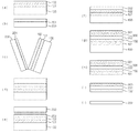
以下、図1及び図2を参照して、本発明による可撓性単結晶フィルムの製造工程を説明する。 Hereinafter, with reference to FIG.1 and FIG.2, the manufacturing process of the flexible single crystal film by this invention is demonstrated.
シリコンベアウェーハをベースウェーハ100及び貼合せウェーハ200として用意する。図2(a)に示すように、シリコン窒化膜(Si3N4)101及びシリコン酸化膜102としての埋め込み絶縁層はベースウェーハの片面に一定の厚さに形成する。前記シリコン酸化膜102は、前記シリコン窒化膜101の上に形成する。このとき、シリコン酸化膜102は、化学気相蒸着方法を用いて製造可能である。図2(b)に示すように、貼合せウェーハ200の表面からの所定の深さに不純物イオンを注入して不純物イオン注入部201を形成する。このとき、不純物としての水素イオンを低電圧イオン注入方法により注入し、注入された水素イオンの投影飛程距離(Rp)が貼合せウェーハの表面から近い、例えば、100ないし1000nmの範囲内になるようにする。
A silicon bare wafer is prepared as a
上述のように埋め込み絶縁層が形成されたベースウェーハ100と、水素イオンがその表面に注入された貼合せウェーハ200と、を洗浄し、図2(c)に示すように、ウェーハ100、200を貼り合わせる。このとき、ウェーハ100、200に対して、貼合せ強度を高めるために、親水性の条件下において洗浄を行う。ウェーハ100、200は、洗浄後にできる限り早い内に、図2(c)に示すように、垂直貼合せを行う。垂直貼合せに際しては、ベースウェーハ100と貼合せウェーハ200を向かい合わせた後、ウェーハの一方の端部から次第に貼っていく。図2(d)に示すように、2枚のウェーハを重ね合わせて単一のウェーハを製造する。
The
このようにして貼り合せられたウェーハを低温下で熱処理して、前記貼合せウェーハの不純物イオン注入部を図2(e)に示すように割る。劈開面をエッチング及びCMP(chemical mechanical polishing)などの方法により処理して所望の厚さに加工することにより、シリコン単結晶層202を製造する(図2(f))。シリコン単結晶層の厚さは、必要に応じて制御可能である。
The wafer bonded in this way is heat-treated at a low temperature, and the impurity ion implanted portion of the bonded wafer is divided as shown in FIG. A silicon
図2(g)に示すように、ベースウェーハ100の上に形成された単結晶層202の上に保護絶縁層300、301を形成する。この保護絶縁層は、ベースウェーハを湿式エッチングにより除去するとき、エッチングされたシリコン単結晶層を保護するための膜であって、先ず、酸化膜300を形成し、その上に窒化膜301を形成する。
As shown in FIG. 2G, protective insulating
シリコン単結晶層の上に保護絶縁層300、301を形成した後、これをKOH溶液により湿式エッチングすると、ベースウェーハが除去される。また、エッチング温度、エッチング溶液の濃度などを調節してエッチング条件を制御することができる。
After the protective insulating
このようにしてベースウェーハが除去されると、図2(h)に示すように、シリコン単結晶層の上下面に絶縁層が残り、単結晶層と絶縁層は薄くなって可撓性を有することになる。このようなフィルムを図2(i)に示すように、HF溶液により湿式エッチングして埋め込み及び保護絶縁層を共に除去すると、シリコン単結晶層のみが残り、図2Jに示すように、シリコンの純粋な可撓性単結晶フィルムが製造される。また、シリコン単結晶層の上に形成された埋め込み絶縁層又は保護絶縁層をエッチングにより除去すると、埋め込み又は保護絶縁層及びシリコン単結晶層よりなる可撓性フィルムを製造することができる。 When the base wafer is removed in this way, as shown in FIG. 2 (h), the insulating layers remain on the upper and lower surfaces of the silicon single crystal layer, and the single crystal layer and the insulating layer become thin and have flexibility. It will be. When such a film is wet-etched with HF solution as shown in FIG. 2 (i) to remove both the buried and protective insulating layers, only the silicon single crystal layer remains, as shown in FIG. 2J. Flexible single crystal films are produced. Further, when the embedded insulating layer or the protective insulating layer formed on the silicon single crystal layer is removed by etching, a flexible film including the embedded or protective insulating layer and the silicon single crystal layer can be manufactured.
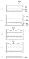
このようにして製造された可撓性フィルムは、その厚さが数十マイクロメートルから数十ナノメートルまで調節可能であるため、図3(a)に示すように、優れた可撓性及び透明特性を有する純粋なシリコン単結晶フィルム202、及び図3(b)に示すように、埋め込み絶縁層102とシリコン単結晶層202よりなる可撓性フィルム203が製造され、これは種々の応用分野に利用可能である。また、可撓性フィルム203の埋め込み絶縁層102は、取り扱い時にシリコン単結晶層202を保護する。
Since the thickness of the flexible film manufactured in this way can be adjusted from several tens of micrometers to several tens of nanometers, as shown in FIG. As shown in FIG. 3B, a pure silicon
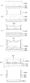
特に、製造されたシリコン単結晶フィルムの可撓度を調べるために、シリコン単結晶の破壊時点までの曲率半径を計算してみた。即ち、図4(a)に示すように、厚さdのシリコンウェーハを曲率半径Rにて折り曲げると、このときに加えられる応力は下記式により表わすことができる。 In particular, in order to investigate the flexibility of the manufactured silicon single crystal film, the radius of curvature up to the point of fracture of the silicon single crystal was calculated. That is, as shown in FIG. 4A, when a silicon wafer having a thickness d is bent at a curvature radius R, the stress applied at this time can be expressed by the following equation.
σ=(d/2R)E(<σy及び<σf) σ = (d / 2R) E (<σ y and <σ f )
ここで、σは応力、dは厚さ、Rは曲率半径、Eは弾性係数、σyは降伏応力、σfは破壊応力を示す。 Here, σ is stress, d is thickness, R is radius of curvature, E is elastic modulus, σ y is yield stress, and σ f is fracture stress.
通常、Eは190GPaであり、σyは6.9GPaであり、σfは2.8GPaである。シリコン単結晶フィルムの厚さが5μmであるとき、破壊個所における理論的な曲率半径は0.17mmであった。本発明による5μmの厚さのシリコン単結晶可撓性フィルムは、少なくとも3mm以下の曲率半径まで破壊無しに曲げることができた(図4(b))。このため、本発明によるシリコン単結晶可撓性フィルムは、所望の通りに十分な有軟性を有することが分かる。同様に、本発明の実施の形態による可撓性単結晶フィルムについても同じことが言える。 Usually, E is 190 GPa, σ y is 6.9 GPa, and σ f is 2.8 GPa. When the thickness of the silicon single crystal film was 5 μm, the theoretical radius of curvature at the fracture location was 0.17 mm. The silicon single crystal flexible film with a thickness of 5 μm according to the present invention could be bent without breaking up to a radius of curvature of at least 3 mm or less (FIG. 4 (b)). For this reason, it turns out that the silicon single crystal flexible film by this invention has sufficient softness as desired. Similarly, the same can be said for the flexible single crystal film according to the embodiment of the present invention.
(実施の形態2) (Embodiment 2)
以下、本発明による、研磨による可撓性単結晶フィルムの製造工程について図5及び図6を参照して説明する。 Hereinafter, the manufacturing process of the flexible single crystal film by grinding | polishing by this invention is demonstrated with reference to FIG.5 and FIG.6.
図6(a)に示すように、ベースウェーハ600、ベースウェーハ600の上に形成された埋め込み絶縁層601、埋め込み絶縁層601の上に形成されたシリコン単結晶層602を有するSOIウェーハを用意する。このSOIウェーハは、SIMOX(separation by implanted oxygen)ウェーハ或いは貼り合わせによるSOIウェーハとして製造可能であり、商業的に販売されるウェーハを用いることもできる。厚い絶縁層を用いる。単結晶層の厚さは、応用分野に応じて調節する。
As shown in FIG. 6A, an SOI wafer having a
このようにして用意されたSOIウェーハの上に酸化膜603と窒化膜604としての保護絶縁層を形成し、これは、ベースウェーハを除去するときにシリコン単結晶層を保護する。先ず、酸化膜603を形成し(図6(b))、酸化膜603の上に窒化膜604を形成する(図6(c))。
A protective insulating layer as an
このようにして形成された保護絶縁層の上に接着剤としてのワックス605を塗布した後(図6(d))、その上に支持ウェーハ606を貼り付ける(図6(e))。このとき、ワックスとしては、水によく溶ける水溶性のものを選ぶことができる。支持ウェーハは、垂直或いは水平貼合せにより貼り付けられる。支持ウェーハ606は、後続する研磨工程中にSOIウェーハを保護し、且つ、工程を容易に行わせるためのものである。即ち、SOIウェーハを研磨するときにウェーハが研磨されながら薄くなってウェーハが研磨用のチャック内において割れるという問題点が生じるが、支持ウェーハを貼り付けた後にSOIウェーハを研磨すると、SOIウェーハが薄く研磨されても割れることなく、ウェーハがチャック内に安全に保持可能である。
A
このようにして支持ウェーハ606が貼り付けられた状態において、図6(f)に示すように、ベースウェーハ600を所定の厚さまで研磨する。このとき、研磨厚さは、例えば、50μmないし200μmに自由に調節することができる。支持ウェーハ606は、研磨後に残っているベースウェーハが厚い場合には用いなくてもよい。
In the state where the
ベースウェーハ600を研磨した後、水溶液或いは化学薬品を用いてワックスを溶かすことにより、支持ウェーハ606を外す(図6(g))。
After polishing the
このようにして支持ウェーハ606を外した後、これに対してKOH溶液による湿式エッチングを行うことにより、研磨されて残っているベースウェーハの残留物600aを除去する(図6(h))。
After removing the
図6(h)に示すように、このようにしてベースウェーハが除去されると、シリコン単結晶層602の上下面に絶縁層604、603、601が残り、この状態において単結晶層と絶縁層の厚さが十分に薄くなって可撓性がある程度確保される。このフィルムをHF溶液により湿式エッチングして、上下面のシリコン単結晶層の上に形成された絶縁層を全て除去することにより、図6(i)に示すように、純粋な可撓性単結晶フィルムが確保される。また、シリコン単結晶層の埋め込み絶縁層又は保護絶縁層をエッチングにより除去すると、絶縁層とシリコン単結晶層よりなる可撓性フィルムが確保される。
As shown in FIG. 6 (h), when the base wafer is removed in this way, the insulating
本発明により可撓性フィルムを製造すると、エッチング時間を大幅に短縮することができる。ベースウェーハを所定の厚さまで研磨することから、エッチング平坦度が良好である。また、本発明による薄型化技術により商業的に市販されるSOIウェーハから可撓性単結晶フィルムを容易に製造することができる。 When a flexible film is produced according to the present invention, the etching time can be greatly shortened. Since the base wafer is polished to a predetermined thickness, the etching flatness is good. In addition, a flexible single crystal film can be easily produced from a commercially available SOI wafer by the thinning technique according to the present invention.
(実施の形態3) (Embodiment 3)
以下、本発明による治具を用いた可撓性単結晶フィルムの製造工程について図8及び図9を参照して説明する。 Hereafter, the manufacturing process of the flexible single crystal film using the jig | tool by this invention is demonstrated with reference to FIG.8 and FIG.9.
先ず、本発明において用いられる治具について説明する。図7に示すように、治具は、上部プレート701と下部プレート700により構成され、上部プレートと下部プレートとの間にウェーハ706が設けられる。これらの各プレート700、701は化学薬品に安定した物質、例えば、登録商標であるテフロンにより製造される。上部プレート701は、上部プレートと下部プレートが組み合わせられた場合、化学物質溶液が入れられる容器702を提供する。容器702の底面は、エッチングにより露出されたウェーハの部分に連通する貫通ホールを備える。ウェーハ及び貫通ホールは密封される。容器702の貫通ホールは、チューブ又は四角筒状、円筒状などの種々の形状に製作される。上部プレートと下部プレートを固定するための取付具703が備えられる。
First, the jig used in the present invention will be described. As shown in FIG. 7, the jig includes an upper plate 701 and a
このような治具を用いると、ウェーハの片面だけを湿式エッチングして除去することができる。即ち、エッチングにより除去すべきウェーハ面が上部プレート701に対面するように、ウェーハ706を下部プレート700の上に載せる。上部プレートと下部プレートを組み合わせた後、容器702にエッチング液を供給してウェーハの表面を除去する。このとき、エッチングの条件に応じて、登録商標であるテフロンが塗布されたヒーター704と温度計705を容器内に設け、エッチング温度を調節する。
When such a jig is used, only one surface of the wafer can be removed by wet etching. That is, the
以下、治具を用いてベースウェーハの一方の全面をエッチングする過程を図8を参照して説明する。 Hereinafter, a process of etching one whole surface of the base wafer using a jig will be described with reference to FIG.
図8(a)に示すように、エッチングすべき面が上に来るようにして、ベースウェーハ800、ベースウェーハ800の上に形成された絶縁層801、絶縁層の上に形成されたシリコン単結晶層802を有するSOIウェーハを用意する。図8(b)に示すように、エッチングにより除去されたベースウェーハの全面が上部プレートの容器において露出されるようにSOIウェーハエッジを治具を用いて保持する。
As shown in FIG. 8A , the
図8(c)に示すように、エッチングにより除去されたベースウェーハの露出面にKOH溶液900を供給する。KOH溶液900を排出した後、露出面にHF溶液901を供給して絶縁層801をエッチングすることにより、純粋なシリコン単結晶の可撓性フィルムを製造する(図8(e))。このとき、HF溶液による絶縁層の除去は、HF溶液中に治具による保持なしに全体のSOIウェーハを担持して行うこともできる。
As shown in FIG. 8C, a
また、前記ステップにおいてKOHエッチングのみを行った後、絶縁層とシリコン単結晶層よりなる可撓性フィルムを製造することができる。 In addition, after performing only KOH etching in the above step, a flexible film composed of an insulating layer and a silicon single crystal layer can be manufactured.
以下、治具を用いてベースウェーハの一部をエッチングして除去する工程を図9を参照して詳細に説明する。 Hereinafter, a process of etching and removing a part of the base wafer using a jig will be described in detail with reference to FIG.
図9(a)に示すように、ベースウェーハ800、ベースウェーハ800の上に形成された絶縁層801、絶縁層の上に形成されたシリコン単結晶層802を有するSOIウェーハを用意する。エッチングにより除去された表面の一部が露出されるようにSOIウェーハの裏面の周縁部を治具により押し付ける(図9(b))。
As shown in FIG. 9A, an SOI wafer having a
図9(c)に示すように、ベースウェーハの露出面にKOH溶液を供給し、ベースウェーハをエッチングして除去する。KOH溶液を排出した後、露出面にHF溶液を供給して絶縁層をエッチングして除去する(図9(d)−1)。即ち、ベースウェーハの露出面はエッチングにより除去され、絶縁層はエッチング保護層の役割を果たす。このとき、HF溶液による絶縁層の除去は、HF溶液中に治具による保持なしに全体のSOIウェーハを担持して行うこともできる(図9(d)−2)。 As shown in FIG. 9C, a KOH solution is supplied to the exposed surface of the base wafer, and the base wafer is etched away. After discharging the KOH solution, an HF solution is supplied to the exposed surface and the insulating layer is etched away (FIG. 9 (d) -1). That is, the exposed surface of the base wafer is removed by etching, and the insulating layer serves as an etching protective layer. At this time, the removal of the insulating layer with the HF solution can be performed by supporting the entire SOI wafer in the HF solution without being held by a jig (FIG. 9 (d) -2).
このように、エッチングにより除去されずに残っているベースウェーハの周縁部を切断して純粋なシリコン単結晶の可撓性フィルムを製造する(図9(e))。 In this way, a pure silicon single crystal flexible film is manufactured by cutting the peripheral edge of the base wafer that remains without being removed by etching (FIG. 9E).
また、前記ステップにおいて、KOHエッチングのみを行った後、ベースウェーハの周縁部を切断すると、絶縁層とシリコン単結晶層よりなる可撓性フィルムを製造することができる。 Moreover, in the said step, after performing only KOH etching, if the peripheral part of a base wafer is cut | disconnected, the flexible film which consists of an insulating layer and a silicon single crystal layer can be manufactured.
可撓性単結晶フィルムは、前記治具を用い、ウェーハの片面のみをエッチングにより除去して容易に製造することができる。即ち、別途の工程なしにベースウェーハを治具を用いてエッチングするため、工数を減らすことができる。また、不要なウェーハの周縁部を容易に除去することができる。上部プレートの容器の形状を変化させて所望の形状の可撓性フィルムを製造することができる。即ち、円形のウェーハの周縁部を四角筒状の容器を持った治具を用いて保持してエッチングした後、周縁部を切断すると、四角形状の可撓性単結晶フィルムが得られる。 The flexible single crystal film can be easily manufactured by using the jig and removing only one surface of the wafer by etching. That is, since the base wafer is etched using a jig without a separate process, the number of steps can be reduced. In addition, unnecessary peripheral portions of the wafer can be easily removed. A flexible film having a desired shape can be produced by changing the shape of the container of the upper plate. That is, a rectangular flexible single crystal film can be obtained by holding and etching the peripheral edge of a circular wafer using a jig having a rectangular cylindrical container and then cutting the peripheral edge.
(実施の形態4) (Embodiment 4)
以下、本発明による研磨と治具を用いた可撓性単結晶フィルムの製造工程について図10ないし図13を参照して説明する。 Hereinafter, the manufacturing process of the flexible single crystal film using the grinding | polishing and jig | tool by this invention is demonstrated with reference to FIG.
図11(a)に示すように、ベースウェーハ1000、ベースウェーハ1000の上に形成された埋め込み絶縁層1001、埋め込み絶縁層1001の上に形成されたシリコン単結晶層1002を有するSOIウェーハ1007を用意する。単結晶層の厚さは、応用分野に応じて調節する。
As shown in FIG. 11A, an
このようにして用意されたSOIウェーハの上にワックス1005を塗布した後(図11(b))、その上に支持ウェーハ1006を貼り付ける(図11(c))。このとき、ワックスとしては、水にもよく溶ける水溶性のものを選ぶことができる。支持ウェーハ1006は、垂直或いは水平貼合せにより貼り付けられる。支持ウェーハ1006は、後続する研磨工程中にSOIウェーハを保護し、且つ、工程を容易に行わせるためのものである。即ち、保護絶縁層は、上述のSOIウェーハの上に形成可能である。
After applying the
図11(d)に示すように、支持ウェーハ1006が貼り付けられた状態において、ベースウェーハ1000を所定の厚さまで研磨する。このとき、研磨厚さは、例えば、50μmないし200μmに自由に調節することができる。
As shown in FIG. 11D, the
ベースウェーハ1000を研磨した後、図12及び図13に示すように、ベースウェーハの残留物1000bを図7に示す治具を用いて湿式エッチングして除去することができる。ベースウェーハの残留物1000bを除去する前後に、水溶液或いは化学薬品を用いてワックスを溶かすことにより、支持ウェーハ1006を外す。
After polishing the
以下、治具を用いてベースウェーハの全面をエッチングする除去工程を図12を参照して説明する。 Hereinafter, the removal process of etching the entire surface of the base wafer using a jig will be described with reference to FIG.
図12(a)に示すように、エッチングにより除去されたベースウェーハの残留物1000bの全面が上部プレート701の容器702において露出されるように、SOIウェーハの周縁を治具により保持する。
As shown in FIG. 12A, the periphery of the SOI wafer is held by a jig so that the entire surface of the
図12(b)に示すように、ベースウェーハをエッチングして除去するために、ベースウェーハの残留物1000bの露出面にKOH溶液900を供給する。KOH溶液900を排出した後、露出面にHF溶液901を供給して絶縁層1001をエッチングして除去する(図12(c))。HF溶液901を排出した後、ワックス1005と支持ウェーハ1006を除去して純粋なシリコン単結晶可撓性フィルムを製造する(図12(d)、図12(e))。支持ウェーハ1006は、ベースウェーハの残留物1000bを除去する前に除去することができる。
As shown in FIG. 12B, in order to etch and remove the base wafer, a
前記ステップにおいて、KOHエッチングのみを行った後、絶縁層とシリコン単結晶層よりなる可撓性フィルムを製造することができる。 In the above step, after performing only KOH etching, a flexible film composed of an insulating layer and a silicon single crystal layer can be manufactured.
以下、図13を参照して、治具を用いてベースウェーハの一部をエッチングして除去する工程を詳細に説明する。本発明に従い可撓性フィルムが製造されると、ウェーハの周縁部を湿式エッチングする必要がない。即ち、所望の形状に応じて容器の貫通ホールの形状が変わる治具を用いてウェーハの所要部分をエッチングし、未エッチングのウェーハの不要な周縁部を切断して所望の形状の可撓性フィルムを製造することができる。このとき、支持ウェーハ1006の切断工程を避けるために、エッチング工程前にワックス1005と支持ウェーハ1006を除去することができる。他の方法として、エッチング工程後に、ウェーハの不要な周縁部の切断前に支持ウェーハ1006を除去することができる。
Hereinafter, with reference to FIG. 13, a process of etching and removing a part of the base wafer using a jig will be described in detail. When the flexible film is manufactured according to the present invention, it is not necessary to wet-etch the peripheral edge of the wafer. That is, a flexible film having a desired shape is formed by etching a required portion of a wafer using a jig that changes the shape of the through hole of the container according to the desired shape, and cutting an unnecessary peripheral portion of the unetched wafer. Can be manufactured. At this time, in order to avoid the cutting process of the
上述のように、ベースウェーハ1000を所定の厚さまで研磨した後、水溶液或いは化学薬品を用いてワックスを溶かすことにより支持ウェーハ1006を外す。支持ウェーハ1006を外した後、エッチングにより除去されたベースウェーハの一部が露出されるようにウェーハの周縁部を治具を用いて押し付ける(図13(a))。
As described above, after polishing the
ベースウェーハを図13(b)に示すようにエッチングして除去するために、ベースウェーハの残留物1000bの露出面にKOH溶液900を供給する。KOH溶液を排出した後、露出面にHF溶液901を供給して絶縁層をエッチングして除去する(図13(c))。HF溶液901を排出すれば、ベースウェーハの周縁部1000cはエッチングにより除去されないため(図13(d))、これを切断して(図13(e))純粋なシリコン単結晶可撓性フィルムを得る(図13(f))。
In order to remove the base wafer by etching as shown in FIG. 13B, a
また、前記ステップにおいて、KOHエッチングのみを行った後、ベースウェーハの周縁部1000cを切断して絶縁層及びシリコン単結晶層よりなる可撓性フィルムを得ることができる。
In the above step, after performing only KOH etching, the
(実施の形態5) (Embodiment 5)
以下、図14ないし図16を参照して、本発明による可撓性単結晶フィルムの製造工程の更に他の実施の形態を詳細に説明する。この実施の形態は、支持ウェーハがSOIウェーハに貼り付けられていない点を除いては、実施の形態4とほとんど同様である。 Hereinafter, still another embodiment of the manufacturing process of the flexible single crystal film according to the present invention will be described in detail with reference to FIGS. This embodiment is almost the same as the fourth embodiment except that the support wafer is not attached to the SOI wafer.
図15(a)に示すように、ベースウェーハ1200、ベースウェーハ1200の上に形成された埋め込み絶縁層1201、及び埋め込み絶縁層1201の上に形成されたシリコン単結晶層1202を有するSOIウェーハを用意する。単結晶層の厚さは、応用分野に応じて調節する。
As shown in FIG. 15A, an SOI wafer having a
保護絶縁層は、上述のSOIウェーハの上に形成される。保護絶縁層は、ベースウェーハが湿式エッチングにより除去されるとき、エッチングからシリコン単結晶層を保護する。この保護絶縁層は、酸化膜1203(図15(b))及びその上に形成された窒化膜1204(図15(c))を備える。 The protective insulating layer is formed on the above-described SOI wafer. The protective insulating layer protects the silicon single crystal layer from etching when the base wafer is removed by wet etching. This protective insulating layer includes an oxide film 1203 (FIG. 15B) and a nitride film 1204 (FIG. 15C) formed thereon.
保護絶縁層をSOIウェーハに形成した後、ベースウェーハ1200を所望の厚さまで研磨する(図15(d))。この実施の形態においては、支持ウェーハをSOIウェーハに貼り付けないため、研磨時にSOIウェーハが研磨用のチャックにおいて割れることがある。このため、研磨後に、ベースウェーハの残留物を厚くする。即ち、研磨時の厚さを150μm以上の所望の厚さに調節することができる。
After the protective insulating layer is formed on the SOI wafer, the
図16に示すように、ベースウェーハ1200を研磨した後、図7に示す治具を用いてベースウェーハの残留物1200bを湿式エッチングして除去することができる。
As shown in FIG. 16, after the
図16は、治具を用いてベースウェーハの一部をエッチングして除去する工程を示す。本発明により可撓性フィルムを製造すると、ウェーハの周縁部を湿式エッチングする必要がない。即ち、所望の形状に応じて容器の貫通ホールの形状が変わる治具を用いてウェーハの所要部分をエッチングし、未エッチングのウェーハの不要な周縁部を切断して所望の形状の可撓性フィルムを製造することができる。 FIG. 16 shows a step of removing a part of the base wafer by etching using a jig. When a flexible film is manufactured according to the present invention, there is no need to wet etch the peripheral edge of the wafer. That is, a flexible film having a desired shape is formed by etching a required portion of a wafer using a jig that changes the shape of the through hole of the container according to the desired shape, and cutting an unnecessary peripheral portion of the unetched wafer. Can be manufactured.
図15(d)に示すように、所定の厚さまでベースウェーハ1200を研磨した後、エッチングにより除去されたベースウェーハの一部が露出されるようにウェーハの周縁部を治具を用いて押し付ける(図16(a))。
As shown in FIG. 15 ( d ), after polishing the
図16(b)に示すように、ベースウェーハをエッチングして除去するために、ベースウェーハの露出面にKOH溶液900を供給する。KOH溶液900を排出した後、露出面にHF溶液を供給して絶縁層1201をエッチングして除去する(図16(c)、図16(d))。また、前記ステップにおいて、KOHエッチングのみを行った後、絶縁層及びシリコン単結晶層よりなる可撓性フィルムを得ることができる。
As shown in FIG. 16B, in order to etch and remove the base wafer, a
絶縁層1201を除去した後、エッチングにより除去されないウェーハの周縁部を切断してシリコン単結晶層と保護絶縁層よりなるウェーハを得る(図16(e))。保護絶縁層1203、1204を除去するために、ウェーハをひっくり返して保護絶縁層1204の全面が露出されるように治具により保持する。その後、HF溶液901を用いて保護絶縁層1203、1204をエッチングして(図16(f))シリコン単結晶可撓性フィルムを得る(図16(g))。
After the insulating
HF溶液による埋め込み絶縁層1201と保護絶縁層1203、1204の除去は、HF溶液中に治具による保持なしに全体のウェーハを担持して行うこともできる。
The removal of the buried insulating
この実施の形態においては、ウェーハの周縁部を治具により保持して研磨した後、ベースウェーハの残留物を除去する方法を説明したが、ベースウェーハの一部をエッチングして周縁部を切断して研磨した後、ウェーハのエッジを治具により保持してベースウェーハの残留物の全面を露出させた後、KOHを用いてエッチングすることができる。 In this embodiment, the method of removing the residue of the base wafer after polishing the peripheral portion of the wafer by holding it with a jig has been explained. However, the peripheral portion is cut by etching a part of the base wafer. After polishing, the edge of the wafer is held by a jig to expose the entire surface of the residue of the base wafer, and then etched using KOH.
(実施の形態6) (Embodiment 6)
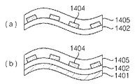
図17及び図18を参照して、本発明による可撓性単結晶フィルムの製造工程を詳細に説明する。 With reference to FIG.17 and FIG.18, the manufacturing process of the flexible single crystal film by this invention is demonstrated in detail.
図17(a)に示すように、ベースウェーハ1400、ベースウェーハの上に形成された絶縁層1401、及び絶縁層の上に形成されたシリコン単結晶層1402を有するSOIウェーハ1406を用意する。
As shown in FIG. 17A, an
このSOIウェーハの単結晶層に通常の半導体製造工程を用いて各種の電子素子を製造する(図17(b))。このような電子素子1404は、目的に応じて所望のように製造可能である。即ち、この種の電子素子は各種のトランジスター、TFTアレイ、ロジック回路などの所望の特性に応じて設計され、半導体の製造工程により製造可能である。
Various electronic elements are manufactured on the single crystal layer of the SOI wafer by using a normal semiconductor manufacturing process (FIG. 17B). Such an
各種の素子が製造された素子層の上に素子を保護するための保護膜1405を形成する(図17(c))。保護膜1405としては、通常のパッシべーション膜、有機物絶縁層などを用いることができる。
A
素子が製造されたSOIウェーハからベースウェーハ1400を除去して可撓性フィルムを製造する(図17(d))。このとき、ベースウェーハの除去は、前記実施の形態1ないし実施の形態5の方法と同様にして行うことができる。
The
図18に示すように、このようにして製造された可撓性フィルムは、シリコン単結晶の上に製造された所望の電子素子だけで十分に可撓性を有する。図18(a)は、純粋なシリコン単結晶層の上に素子が製造された可撓性フィルムを示し、図18(b)は、絶縁層とシリコン単結晶層よりなる可撓性フィルムの上に素子が製造された様子を示し、絶縁層が取り扱い時にシリコン単結晶層及び素子を保護することになる。 As shown in FIG. 18, the flexible film manufactured in this way is sufficiently flexible only with a desired electronic device manufactured on a silicon single crystal. FIG. 18 (a) shows a flexible film in which a device is manufactured on a pure silicon single crystal layer, and FIG. 18 (b) shows a film on the flexible film composed of an insulating layer and a silicon single crystal layer. Fig. 5 shows a state in which the device is manufactured, and the insulating layer protects the silicon single crystal layer and the device during handling.
上述のように、本発明の可撓性単結晶フィルムは、シリコン単結晶の上に製造された所望の特性の素子を容易に製造することができ、しかも、全体の可撓性を許容する。特に、単結晶ウェーハを用いて可撓性単結晶フィルムを容易に製造することができる。 As described above, the flexible single crystal film of the present invention can easily manufacture an element having desired characteristics manufactured on a silicon single crystal and allows the entire flexibility. In particular, a flexible single crystal film can be easily manufactured using a single crystal wafer.
本発明によれば、単結晶層に所望の各種の電子素子が製造された可撓性フィルムを単純な方法により安定して製造する。本発明は、電子素子の所望の特性を具現することができる。即ち、単結晶層の上に各種の電子素子を製造することから、単結晶層から素子用のアクティブ層を形成する。半導体の製造工程を用いることから、1000cm2/Vsecと極めて高い電子移動値が得られる。このように、優れた電子素子の特性を得ることができ、漏れ電流も大幅に低減することができる。また、各種の電子素子のサイズを通常の半導体素子レベルにコンパクト化することが可能である。シリコンウェーハを通じた半導体の製造工程を適用することから、安定した高温工程と優れた整列正確度が両立可能な半導体フォトリソグラフィ及びエッチング工程により、現在の半導体工程における30nmまでのデザインルールにて回路を設計することが可能である。 According to the present invention, a flexible film in which various desired electronic elements are manufactured on a single crystal layer is stably manufactured by a simple method. The present invention can embody desired characteristics of an electronic device. That is, since various electronic devices are manufactured on the single crystal layer, an active layer for the device is formed from the single crystal layer. Since a semiconductor manufacturing process is used, an extremely high electron transfer value of 1000 cm 2 / Vsec can be obtained. Thus, excellent electronic device characteristics can be obtained, and leakage current can be greatly reduced. In addition, the size of various electronic elements can be reduced to the level of a normal semiconductor element. Since the semiconductor manufacturing process through the silicon wafer is applied, the circuit can be configured with the design rule up to 30 nm in the current semiconductor process by the semiconductor photolithography and etching process that can achieve both stable high temperature process and excellent alignment accuracy. It is possible to design.
そして、本発明は、単結晶の安定したチャンネル素子を使用できることから、全ての駆動回路を一体化させたSOP(system on panel)及びその他のメモリ、システムIC、プロセッサーなどをはじめとする特定の用途の半導体回路を一体化させることができ、上記のごとき素子を可撓性フィルムに実現することが可能になる。 Since the present invention can use a stable single-crystal channel element, it can be used for specific applications such as SOP (system on panel) and other memories, system ICs, processors, etc. in which all drive circuits are integrated. These semiconductor circuits can be integrated, and the element as described above can be realized in a flexible film.
適切な薄型化技術を用いて可撓性単結晶フィルムを製造することができ、可撓性単結晶フィルムを製造する製造工程を単純化させることで、生産性を高めて製造コストを削減することができる。 A flexible single crystal film can be manufactured using appropriate thinning technology, and the manufacturing process for manufacturing the flexible single crystal film is simplified to increase productivity and reduce manufacturing costs. Can do.
以上、本発明を具体的な実施の形態を通じて詳細に説明したが、本発明は、これに限定されるものではなく、本発明の技術的な思想内において当分野における通常の知識を持った者によりその変形や改良が可能である。 The present invention has been described in detail through specific embodiments. However, the present invention is not limited to this, and those who have ordinary knowledge in the field within the technical idea of the present invention. The deformation and improvement are possible.
Claims (36)
前記ベースウェーハに1以上の埋め込み絶縁層を形成するステップと、
前記貼合せウェーハに水素イオンを注入するステップと、
前記ベースウェーハと貼合せウェーハを貼り合わせるステップと、
前記貼合せウェーハを割るステップと、
前記貼合せウェーハの劈開面をエッチングすることにより、ベースウェーハの埋め込み絶縁層の上に単結晶層が形成されたSOIウェーハを製造するステップと、
前記単結晶層の上に酸化膜および窒化膜を積層形成して1以上の保護絶縁層を形成するステップと、
前記ベースウェーハを湿式エッチングして除去するステップと、
HFを用いた湿式エッチング方法により1以上の絶縁層を除去するステップと、
を含むことを特徴とする可撓性フィルムの製造方法。 Preparing a base wafer and a bonded wafer;
Forming one or more buried insulating layers on the base wafer;
Implanting hydrogen ions into the bonded wafer;
Bonding the base wafer and the bonded wafer;
Breaking the bonded wafer;
Etching the cleaved surface of the bonded wafer to produce an SOI wafer having a single crystal layer formed on the buried insulating layer of the base wafer;
Stacking an oxide film and a nitride film on the single crystal layer to form one or more protective insulating layers;
Removing the base wafer by wet etching ;
Removing one or more insulating layers by a wet etching method using HF ;
A method for producing a flexible film, comprising:
前記ベースウェーハの上に窒化膜を形成するステップと、
前記窒化膜の上に酸化膜を形成するステップと、を更に含むことを特徴とする請求項1記載の可撓性フィルムの製造方法。Forming one or more buried insulating layers on the base wafer;
Forming a nitride film on the base wafer;
Method for manufacturing a flexible film according to claim 1, further comprising the steps of: forming an oxide film on the nitride film.
前記ベースウェーハに1以上の埋め込み絶縁層を形成するステップと、
前記貼合せウェーハに水素イオンを注入するステップと、
前記ベースウェーハと貼合せウェーハを貼り合わせるステップと、
前記貼合せウェーハを割るステップと、
前記貼合せウェーハの劈開面をエッチングすることにより、ベースウェーハの埋め込み絶縁層の上に単結晶層が形成されたSOIウェーハを製造するステップと、
前記単結晶層の上に酸化膜および窒化膜を積層形成して1以上の保護絶縁層を形成するステップと、
前記ベースウェーハを湿式エッチングして除去するステップと、
HFを用いた湿式エッチング方法により単結晶層の上に形成された前記1以上の埋め込み絶縁層又は前記1以上の保護絶縁層のうちいずれか一方を除去するステップと、
を含むことを特徴とする可撓性フィルムの製造方法。 Preparing a base wafer and a bonded wafer;
Forming one or more buried insulating layers on the base wafer;
Implanting hydrogen ions into the bonded wafer;
Bonding the base wafer and the bonded wafer;
Breaking the bonded wafer;
Etching the cleaved surface of the bonded wafer to produce an SOI wafer having a single crystal layer formed on the buried insulating layer of the base wafer;
Stacking an oxide film and a nitride film on the single crystal layer to form one or more protective insulating layers;
Removing the base wafer by wet etching;
Removing either one of the one or more buried insulator layers or said one or more protective insulating layer formed on the single crystal layer by wet etching method using H F,
Method for producing a flexible film you comprising a.
前記ベースウェーハに1以上の埋め込み絶縁層を形成するステップと、
前記貼合せウェーハに水素イオンを注入するステップと、
前記ベースウェーハと貼合せウェーハを貼り合わせるステップと、
前記貼合せウェーハを割るステップと、
前記貼合せウェーハの劈開面をエッチングすることにより、ベースウェーハの埋め込み絶縁層の上に単結晶層が形成されたSOIウェーハを製造するステップと、
前記単結晶層の上に酸化膜および窒化膜を積層形成して1以上の保護絶縁層を形成するステップと、
前記ベースウェーハを所望の厚さに研磨するステップと、
ベースウェーハを湿式エッチングして研磨した後、ベースウェーハの残留物を除去するステップと、
HFを用いた湿式エッチング方法により1以上の絶縁層を除去するステップと、
を含むことを特徴とする可撓性フィルムの製造方法。 Preparing a base wafer and a bonded wafer;
Forming one or more buried insulating layers on the base wafer;
Implanting hydrogen ions into the bonded wafer;
Bonding the base wafer and the bonded wafer;
Breaking the bonded wafer;
Etching the cleaved surface of the bonded wafer to produce an SOI wafer having a single crystal layer formed on the buried insulating layer of the base wafer;
Stacking an oxide film and a nitride film on the single crystal layer to form one or more protective insulating layers;
A step of polishing the front SL base wafer to a desired thickness,
Removing the residue of the base wafer after the base wafer is wet etched and polished;
Removing one or more insulating layers by a wet etching method using HF;
Method for producing a flexible film you comprising a.
前記ベースウェーハを研磨する前に、保護絶縁層の上にワックスを塗布して前記SOIウェーハと支持ウェーハを貼り合わせるステップと、
前記ベースウェーハを研磨した後、前記支持ウェーハを除去するステップと、を含むことを特徴とする請求項6記載の可撓性フィルムの製造方法。Removing the base wafer comprises:
Before polishing the base wafer, applying a wax on the protective insulating layer and bonding the SOI wafer and the support wafer;
The method for manufacturing a flexible film according to claim 6 , further comprising: removing the support wafer after polishing the base wafer.
前記SOIウェーハのエッジを治具により保持して前記ベースウェーハの下面の全体が露出されるようにSOIウェーハを保持するステップと、
前記ベースウェーハをエッチングして除去するステップと、
を含むことを特徴とする可撓性フィルムの製造方法。Providing an SOI wafer having a base wafer, one or more insulating layers formed on the base wafer, and a single crystal layer formed on the one or more insulating layers;
Holding the SOI wafer so that the entire lower surface of the base wafer is exposed by holding the edge of the SOI wafer with a jig ;
Etching and removing the base wafer;
A method for producing a flexible film, comprising:
前記SOIウェーハの周縁部を治具により保持してベースウェーハの下面の一部が露出されるようにSOIウェーハを保持するステップと、
前記ベースウェーハをエッチングして除去するステップと、
を含むことを特徴とする可撓性フィルムの製造方法。 Providing an SOI wafer having a base wafer, one or more insulating layers formed on the base wafer, and a single crystal layer formed on the one or more insulating layers;
A step of holding the SOI wafer so that a portion of the lower surface of the base wafer Ru is exposed is held by a jig peripheral portion of the SOI wafer,
Etching and removing the base wafer;
Method for producing a flexible film you comprising a.
前記SOIウェーハの単結晶層と支持ウェーハを貼り合わせるステップと、
前記ベースウェーハ及び前記支持ウェーハを除去するステップと、を含み、
前記ベースウェーハを除去するステップは、
所定の厚さまで前記ベースウェーハを研磨するステップと、
前記支持ウェーハを除去するステップと、
研磨後にベースウェーハの残留物の下部面が露出されるように治具によりSOIウェーハを保持するステップと、
湿式エッチングによりベースウェーハの残留物を除去するステップと、
を含むことを特徴とする可撓性フィルムの製造方法。Comprising the steps of: providing a SOI wafer having the base wafer, one or more buried insulator layer formed on the base wafer, and a single crystal layer formed on said one or more buried insulator layers,
Bonding the single crystal layer of the SOI wafer and a supporting wafer;
Removing the base wafer and the support wafer ,
Removing the base wafer comprises:
Polishing the base wafer to a predetermined thickness;
Removing the support wafer;
Holding the SOI wafer with a jig so that the lower surface of the residue of the base wafer is exposed after polishing;
Removing the residue of the base wafer by wet etching;
A method for producing a flexible film, comprising:
前記SOIウェーハの単結晶層と支持ウェーハを貼り合わせるステップと、
前記ベースウェーハ及び前記支持ウェーハを除去するステップと、
を含み、
前記ベースウェーハを除去するステップは、
所定の厚さまで前記ベースウェーハを研磨するステップと、
研磨後にベースウェーハの残留物の下部面が露出されるように治具によりSOIウェーハを保持するステップと、
湿式エッチングによりベースウェーハの残留物を除去するステップと、
前記支持ウェーハを除去するステップと、
を含むことを特徴とする可撓性フィルムの製造方法。 Providing an SOI wafer having a base wafer, one or more buried insulating layers formed on the base wafer, and a single crystal layer formed on the one or more buried insulating layers;
Bonding the single crystal layer of the SOI wafer and a supporting wafer;
Removing the base wafer and the support wafer;
Including
Removing the base wafer comprises:
Polishing the base wafer to a predetermined thickness;
Holding the SOI wafer with a jig so that the lower surface of the residue of the base wafer is exposed after polishing;
Removing the residue of the base wafer by wet etching;
Removing the support wafer;
Method for producing a flexible film you comprising a.
前記単結晶層の上に1以上の保護絶縁層を形成するステップと、
前記ベースウェーハを所定の厚さに研磨するステップと、
研磨後に、前記SOIウェーハのエッジを治具により保持して前記ベースウェーハの残留物の下面の全体が露出されるようにSOIウェーハを保持するステップと、
ベースウェーハの残留物を湿式エッチングして除去するステップと、
前記1以上の埋め込み絶縁層及び/又は前記1以上の保護絶縁層を除去するステップと、
を含むことを特徴とする可撓性フィルムの製造方法。Comprising the steps of: providing a SOI wafer having the base wafer, one or more buried insulator layer formed on the base wafer, and a single crystal layer formed on said one or more buried insulator layers,
Forming one or more protective insulating layers on the single crystal layer;
Polishing the base wafer to a predetermined thickness;
Holding the SOI wafer so that the entire bottom surface of the residue of the base wafer is exposed by holding the edge of the SOI wafer with a jig after polishing;
Removing the base wafer residue by wet etching;
Removing the one or more buried insulating layers and / or the one or more protective insulating layers;
A method for producing a flexible film, comprising:
前記単結晶層の上に1以上の保護絶縁層を形成するステップと、
前記ベースウェーハを所定の厚さに研磨するステップと、
研磨後に前記SOIウェーハの周縁部を治具により保持して前記ベースウェーハの下面の一部が露出されるようにSOIウェーハを保持するステップと、 前記ベースウェーハの残留物を湿式エッチングして除去した後、治具により保持していた周縁部を切断するステップと、
前記1以上の埋め込み絶縁層及び/又は前記1以上の保護絶縁層を除去するステップと、
を含むことを特徴とする可撓性フィルムの製造方法。 Providing an SOI wafer having a base wafer, one or more buried insulating layers formed on the base wafer, and a single crystal layer formed on the one or more buried insulating layers;
Forming one or more protective insulating layers on the single crystal layer;
Polishing the base wafer to a predetermined thickness;
And a step of holding the SOI wafer so that the periphery of the SOI wafer after polishing is held by jig part of the lower surface of the base wafer Ru is exposed, the residue of the previous SL base wafer by wet etching After removing , cutting the peripheral edge held by the jig ;
Removing the one or more buried insulating layers and / or the one or more protective insulating layers;
Method for producing a flexible film you comprising a.
前記SOIウェーハの前記単結晶層の上にワックスを塗布するステップと、
前記SOIウェーハの前記単結晶層と支持ウェーハを貼り合わせるステップと、を含むことを特徴とする請求項18ないし20いずれか1項に記載の可撓性フィルムの製造方法。The step of attaching a support wafer to the single crystal layer of the SOI wafer includes:
Applying a wax on the single crystal layer of the SOI wafer;
The method for manufacturing a flexible film according to any one of claims 18 to 20 , further comprising a step of bonding the single crystal layer of the SOI wafer and a support wafer.
前記ベースウェーハを研磨する前に、保護絶縁層の上にワックスを塗布するステップと、
SOIウェーハと支持ウェーハを貼り合わせるステップと、を含み、
前記ベースウェーハ及び支持ウェーハを除去した後には、1以上の埋め込み絶縁膜及び1以上の保護絶縁層を除去するステップを更に含むことを特徴とする請求項23記載の可撓性フィルムの製造方法。The step of attaching a support wafer to the single crystal layer of the SOI wafer includes:
Applying a wax over the protective insulating layer before polishing the base wafer;
Bonding the SOI wafer and the support wafer,
24. The method of manufacturing a flexible film according to claim 23 , further comprising the step of removing one or more buried insulating films and one or more protective insulating layers after removing the base wafer and the supporting wafer.
前記単結晶層の上に電子素子を組み付けて1以上の素子層を形成するステップと、
前記素子層の上に素子保護膜を形成するステップと、
前記ベースウェーハを湿式エッチングして除去するステップと、
を含むことを特徴とする可撓性フィルムの製造方法。Providing an SOI wafer having a base wafer, one or more insulating layers formed on the base wafer, and a single crystal layer formed on the one or more insulating layers;
Assembling an electronic element on the single crystal layer to form one or more element layers;
Forming an element protective film on the element layer;
Removing the base wafer by wet etching ;
A method for producing a flexible film, comprising:
前記単結晶層の上に電子素子を組み付けて1以上の素子層を形成するステップと、
前記素子層の上に素子保護膜を形成するステップと、
所定の厚さまでベースウェーハを研磨するステップと、
湿式エッチングにより研磨後、ベースウェーハの残留物を除去するステップと、
を含むことを特徴とする可撓性フィルムの製造方法。 Providing an SOI wafer having a base wafer, one or more insulating layers formed on the base wafer, and a single crystal layer formed on the one or more insulating layers;
Assembling an electronic element on the single crystal layer to form one or more element layers;
Forming an element protective film on the element layer;
A step of polishing the base wafer to Jo Tokoro thickness,
Removing the residue of the base wafer after polishing by wet etching;
Method for producing a flexible film you comprising a.
前記単結晶層の上に電子素子を組み付けて1以上の素子層を形成するステップと、
前記素子層の上に素子保護膜を形成するステップと、
前記ベースウェーハの下面が露出されるように治具によりSOIウェーハを保持するステップと、
ベースウェーハを湿式エッチングして除去するステップと、
を含むことを特徴とする可撓性フィルムの製造方法。 Providing an SOI wafer having a base wafer, one or more insulating layers formed on the base wafer, and a single crystal layer formed on the one or more insulating layers;
Assembling an electronic element on the single crystal layer to form one or more element layers;
Forming an element protective film on the element layer;
A step of holding the SOI wafer with the jig to the lower surface of the front SL base wafer is exposed,
Removing the base wafer by wet etching;
Method for producing a flexible film you comprising a.
前記単結晶層の上に電子素子を組み付けて1以上の素子層を形成するステップと、
前記素子層の上に素子保護膜を形成するステップと、
所定の厚さにベースウェーハを研磨するステップと、
前記ベースウェーハの下面が露出されるように治具によりSOIウェーハを保持するステップと、
前記ベースウェーハを湿式エッチングして除去するステップと、
を含むことを特徴とする可撓性フィルムの製造方法。 Providing an SOI wafer having a base wafer, one or more insulating layers formed on the base wafer, and a single crystal layer formed on the one or more insulating layers;
Assembling an electronic element on the single crystal layer to form one or more element layers;
Forming an element protective film on the element layer;
A step of polishing the base wafer to a Jo Tokoro thickness,
Holding the SOI wafer with a jig so that the lower surface of the base wafer is exposed;
Removing the base wafer by wet etching;
Method for producing a flexible film you comprising a.
1以上の貫通ホールを有する上部プレートと、
前記下部及び上部プレートを組み合わせるための固定手段と、を備え、
基板が前記下部プレートと前記上部プレートとの間に位置するとき、基板のエッチング処理されるべき部分が前記1以上の貫通ホールに露出されるように構成され、前記基板と1以上の貫通ホールは密封され、1以上の前記貫通ホールを介してエッチング溶液が供給されることを特徴とするエッチング用の治具。A lower plate,
An upper plate having one or more through holes;
Fixing means for combining the lower and upper plates,
When the substrate is positioned between the lower plate and the upper plate, a portion of the substrate to be etched is exposed to the one or more through holes, and the substrate and the one or more through holes are An etching jig which is sealed and supplied with an etching solution through one or more of the through holes.
Applications Claiming Priority (3)
| Application Number | Priority Date | Filing Date | Title |
|---|---|---|---|
| US10/833,050 | 2004-04-28 | ||
| US10/833,050 US7592239B2 (en) | 2003-04-30 | 2004-04-28 | Flexible single-crystal film and method of manufacturing the same |
| PCT/KR2004/002286 WO2005106933A1 (en) | 2004-04-28 | 2004-09-09 | Flexible single-crystal film and method of manufacturing the same |
Publications (2)
| Publication Number | Publication Date |
|---|---|
| JP2007535809A JP2007535809A (en) | 2007-12-06 |
| JP4959552B2 true JP4959552B2 (en) | 2012-06-27 |
Family
ID=35241924
Family Applications (1)
| Application Number | Title | Priority Date | Filing Date |
|---|---|---|---|
| JP2007510601A Expired - Lifetime JP4959552B2 (en) | 2004-04-28 | 2004-09-09 | Flexible single crystal film and method for producing the same |
Country Status (4)
| Country | Link |
|---|---|
| EP (1) | EP1751788B1 (en) |
| JP (1) | JP4959552B2 (en) |
| CN (1) | CN100481328C (en) |
| WO (1) | WO2005106933A1 (en) |
Families Citing this family (2)
| Publication number | Priority date | Publication date | Assignee | Title |
|---|---|---|---|---|
| KR101286551B1 (en) | 2009-09-16 | 2013-07-17 | 엘지디스플레이 주식회사 | Flexible substrate and method of fabricating flexible display having the same |
| CN107146830B (en) * | 2017-06-07 | 2019-04-02 | 浙江大学 | A method for preparing flexible and transparent graphene/silicon metal-semiconductor-metal photodetectors |
Family Cites Families (14)
| Publication number | Priority date | Publication date | Assignee | Title |
|---|---|---|---|---|
| JP2857456B2 (en) * | 1990-01-19 | 1999-02-17 | 株式会社リコー | Method for manufacturing semiconductor film |
| JP3250673B2 (en) * | 1992-01-31 | 2002-01-28 | キヤノン株式会社 | Semiconductor element substrate and method of manufacturing the same |
| EP0849788B1 (en) * | 1996-12-18 | 2004-03-10 | Canon Kabushiki Kaisha | Process for producing semiconductor article by making use of a substrate having a porous semiconductor layer |
| KR200174717Y1 (en) * | 1996-12-24 | 2000-04-01 | 신현준 | Silicone Etching Jig |
| US6444487B1 (en) * | 1998-07-28 | 2002-09-03 | Rosemount Aerospace Inc. | Flexible silicon strain gage |
| US6468923B1 (en) * | 1999-03-26 | 2002-10-22 | Canon Kabushiki Kaisha | Method of producing semiconductor member |
| US6452091B1 (en) | 1999-07-14 | 2002-09-17 | Canon Kabushiki Kaisha | Method of producing thin-film single-crystal device, solar cell module and method of producing the same |
| JP2001185528A (en) * | 1999-12-27 | 2001-07-06 | Minolta Co Ltd | Jig for etching, and apparatus and method for etching |
| JP2003218330A (en) * | 2002-01-21 | 2003-07-31 | Matsushita Electric Ind Co Ltd | Semiconductor thin film, thin film semiconductor device, and manufacturing method thereof |
| US6864118B2 (en) * | 2002-01-28 | 2005-03-08 | Hewlett-Packard Development Company, L.P. | Electronic devices containing organic semiconductor materials |
| JP4003546B2 (en) * | 2002-06-10 | 2007-11-07 | ソニー株式会社 | Method for manufacturing SOI substrate and method for manufacturing semiconductor device |
| KR100511656B1 (en) * | 2002-08-10 | 2005-09-07 | 주식회사 실트론 | Method of fabricating nano SOI wafer and nano SOI wafer fabricated by the same |
| KR100547237B1 (en) * | 2003-05-23 | 2006-01-26 | 한양대학교 산학협력단 | Method for manufacturing single crystal flexible film and flexible electro-optical device, apparatus for manufacturing same |
| KR100583429B1 (en) * | 2003-04-30 | 2006-05-24 | 한양대학교 산학협력단 | Flexible single crystal film and its manufacturing method |
-
2004
- 2004-09-09 JP JP2007510601A patent/JP4959552B2/en not_active Expired - Lifetime
- 2004-09-09 CN CNB200480043169XA patent/CN100481328C/en not_active Expired - Fee Related
- 2004-09-09 WO PCT/KR2004/002286 patent/WO2005106933A1/en not_active Ceased
- 2004-09-09 EP EP04774545.0A patent/EP1751788B1/en not_active Expired - Lifetime
Also Published As
| Publication number | Publication date |
|---|---|
| WO2005106933A1 (en) | 2005-11-10 |
| EP1751788A4 (en) | 2010-01-13 |
| EP1751788A1 (en) | 2007-02-14 |
| JP2007535809A (en) | 2007-12-06 |
| CN100481328C (en) | 2009-04-22 |
| CN1957445A (en) | 2007-05-02 |
| EP1751788B1 (en) | 2018-11-28 |
Similar Documents
| Publication | Publication Date | Title |
|---|---|---|
| EP1676310B1 (en) | Method for preparing and assembling substrates | |
| US7459375B2 (en) | Transfer method for forming a silicon-on-plastic wafer | |
| US8241996B2 (en) | Substrate stiffness method and resulting devices for layer transfer process | |
| US7659582B2 (en) | Active silicon device on a cleaved silicon-on-insulator substrate | |
| US8383489B2 (en) | SOI wafer and method for forming the same | |
| JPH08505010A (en) | Method for producing single crystal silicon island on quartz substrate | |
| US7592239B2 (en) | Flexible single-crystal film and method of manufacturing the same | |
| TWI787565B (en) | Process for transferring a superficial layer to cavities | |
| CN113437162A (en) | Preparation method of substrate structure of hybrid integrated photoelectric chip and substrate structure | |
| JP4959552B2 (en) | Flexible single crystal film and method for producing the same | |
| KR100583429B1 (en) | Flexible single crystal film and its manufacturing method | |
| TWI800699B (en) | Method of fabricating a device comprising a membrane overhanging a cavity | |
| JP2006012914A (en) | Integrated circuit chip manufacturing method and semiconductor device | |
| JP4468107B2 (en) | Semiconductor device manufacturing method, semiconductor device, and semiconductor circuit substrate | |
| CN110098145A (en) | Monocrystalline silicon thin film and preparation method thereof | |
| KR100612885B1 (en) | Method of manufacturing a substrate in which a single monocrystalline silicon layer is integrated | |
| JP2000150379A (en) | Method for manufacturing laminated body having crystalline semiconductor layer | |
| JP2576250B2 (en) | Thin film element forming method and thin film element structure |
Legal Events
| Date | Code | Title | Description |
|---|---|---|---|
| A521 | Request for written amendment filed |
Free format text: JAPANESE INTERMEDIATE CODE: A523 Effective date: 20091029 |
|
| A131 | Notification of reasons for refusal |
Free format text: JAPANESE INTERMEDIATE CODE: A131 Effective date: 20110118 |
|
| A521 | Request for written amendment filed |
Free format text: JAPANESE INTERMEDIATE CODE: A523 Effective date: 20110414 |
|
| A131 | Notification of reasons for refusal |
Free format text: JAPANESE INTERMEDIATE CODE: A131 Effective date: 20110628 |
|
| A521 | Request for written amendment filed |
Free format text: JAPANESE INTERMEDIATE CODE: A523 Effective date: 20110926 |
|
| A131 | Notification of reasons for refusal |
Free format text: JAPANESE INTERMEDIATE CODE: A131 Effective date: 20111025 |
|
| A521 | Request for written amendment filed |
Free format text: JAPANESE INTERMEDIATE CODE: A523 Effective date: 20120119 |
|
| TRDD | Decision of grant or rejection written | ||
| A01 | Written decision to grant a patent or to grant a registration (utility model) |
Free format text: JAPANESE INTERMEDIATE CODE: A01 Effective date: 20120221 |
|
| A01 | Written decision to grant a patent or to grant a registration (utility model) |
Free format text: JAPANESE INTERMEDIATE CODE: A01 |
|
| A61 | First payment of annual fees (during grant procedure) |
Free format text: JAPANESE INTERMEDIATE CODE: A61 Effective date: 20120321 |
|
| FPAY | Renewal fee payment (event date is renewal date of database) |
Free format text: PAYMENT UNTIL: 20150330 Year of fee payment: 3 |
|
| R150 | Certificate of patent or registration of utility model |
Ref document number: 4959552 Country of ref document: JP Free format text: JAPANESE INTERMEDIATE CODE: R150 Free format text: JAPANESE INTERMEDIATE CODE: R150 |
|
| R250 | Receipt of annual fees |
Free format text: JAPANESE INTERMEDIATE CODE: R250 |
|
| R250 | Receipt of annual fees |
Free format text: JAPANESE INTERMEDIATE CODE: R250 |
|
| R250 | Receipt of annual fees |
Free format text: JAPANESE INTERMEDIATE CODE: R250 |
|
| R250 | Receipt of annual fees |
Free format text: JAPANESE INTERMEDIATE CODE: R250 |
|
| R250 | Receipt of annual fees |
Free format text: JAPANESE INTERMEDIATE CODE: R250 |
|
| R250 | Receipt of annual fees |
Free format text: JAPANESE INTERMEDIATE CODE: R250 |