JP4955334B2 - Acceleration sensor - Google Patents
Acceleration sensor Download PDFInfo
- Publication number
- JP4955334B2 JP4955334B2 JP2006212352A JP2006212352A JP4955334B2 JP 4955334 B2 JP4955334 B2 JP 4955334B2 JP 2006212352 A JP2006212352 A JP 2006212352A JP 2006212352 A JP2006212352 A JP 2006212352A JP 4955334 B2 JP4955334 B2 JP 4955334B2
- Authority
- JP
- Japan
- Prior art keywords
- chip
- heat generating
- sensor
- thermocouple
- sensor chip
- Prior art date
- Legal status (The legal status is an assumption and is not a legal conclusion. Google has not performed a legal analysis and makes no representation as to the accuracy of the status listed.)
- Expired - Fee Related
Links
- 230000001133 acceleration Effects 0.000 title claims description 68
- 238000010438 heat treatment Methods 0.000 claims description 32
- 239000000463 material Substances 0.000 claims description 17
- 239000002184 metal Substances 0.000 claims description 12
- 229910052751 metal Inorganic materials 0.000 claims description 12
- 239000010931 gold Substances 0.000 claims description 9
- 239000011347 resin Substances 0.000 claims description 9
- 229920005989 resin Polymers 0.000 claims description 9
- ATJFFYVFTNAWJD-UHFFFAOYSA-N Tin Chemical compound [Sn] ATJFFYVFTNAWJD-UHFFFAOYSA-N 0.000 claims description 2
- 230000008878 coupling Effects 0.000 claims description 2
- 238000010168 coupling process Methods 0.000 claims description 2
- 238000005859 coupling reaction Methods 0.000 claims description 2
- PCHJSUWPFVWCPO-UHFFFAOYSA-N gold Chemical compound [Au] PCHJSUWPFVWCPO-UHFFFAOYSA-N 0.000 claims description 2
- 229910052737 gold Inorganic materials 0.000 claims description 2
- 230000020169 heat generation Effects 0.000 claims description 2
- 238000007789 sealing Methods 0.000 claims description 2
- 238000001514 detection method Methods 0.000 claims 1
- 230000005855 radiation Effects 0.000 description 12
- 238000004519 manufacturing process Methods 0.000 description 9
- 239000000758 substrate Substances 0.000 description 4
- 239000003570 air Substances 0.000 description 2
- 238000000034 method Methods 0.000 description 2
- 230000035945 sensitivity Effects 0.000 description 2
- 206010037660 Pyrexia Diseases 0.000 description 1
- 239000012080 ambient air Substances 0.000 description 1
- 238000010586 diagram Methods 0.000 description 1
- 238000002844 melting Methods 0.000 description 1
- 230000008018 melting Effects 0.000 description 1
- 230000002093 peripheral effect Effects 0.000 description 1
- 239000004065 semiconductor Substances 0.000 description 1
Images


Classifications
-
- G—PHYSICS
- G01—MEASURING; TESTING
- G01P—MEASURING LINEAR OR ANGULAR SPEED, ACCELERATION, DECELERATION, OR SHOCK; INDICATING PRESENCE, ABSENCE, OR DIRECTION, OF MOVEMENT
- G01P1/00—Details of instruments
- G01P1/02—Housings
- G01P1/023—Housings for acceleration measuring devices
-
- G—PHYSICS
- G01—MEASURING; TESTING
- G01P—MEASURING LINEAR OR ANGULAR SPEED, ACCELERATION, DECELERATION, OR SHOCK; INDICATING PRESENCE, ABSENCE, OR DIRECTION, OF MOVEMENT
- G01P15/00—Measuring acceleration; Measuring deceleration; Measuring shock, i.e. sudden change of acceleration
- G01P15/006—Measuring acceleration; Measuring deceleration; Measuring shock, i.e. sudden change of acceleration by making use of fluid seismic masses
- G01P15/008—Measuring acceleration; Measuring deceleration; Measuring shock, i.e. sudden change of acceleration by making use of fluid seismic masses by using thermal pick-up
-
- G—PHYSICS
- G01—MEASURING; TESTING
- G01P—MEASURING LINEAR OR ANGULAR SPEED, ACCELERATION, DECELERATION, OR SHOCK; INDICATING PRESENCE, ABSENCE, OR DIRECTION, OF MOVEMENT
- G01P15/00—Measuring acceleration; Measuring deceleration; Measuring shock, i.e. sudden change of acceleration
- G01P15/02—Measuring acceleration; Measuring deceleration; Measuring shock, i.e. sudden change of acceleration by making use of inertia forces using solid seismic masses
- G01P15/08—Measuring acceleration; Measuring deceleration; Measuring shock, i.e. sudden change of acceleration by making use of inertia forces using solid seismic masses with conversion into electric or magnetic values
- G01P15/0802—Details
-
- G—PHYSICS
- G01—MEASURING; TESTING
- G01P—MEASURING LINEAR OR ANGULAR SPEED, ACCELERATION, DECELERATION, OR SHOCK; INDICATING PRESENCE, ABSENCE, OR DIRECTION, OF MOVEMENT
- G01P15/00—Measuring acceleration; Measuring deceleration; Measuring shock, i.e. sudden change of acceleration
- G01P15/18—Measuring acceleration; Measuring deceleration; Measuring shock, i.e. sudden change of acceleration in two or more dimensions
-
- H—ELECTRICITY
- H01—ELECTRIC ELEMENTS
- H01L—SEMICONDUCTOR DEVICES NOT COVERED BY CLASS H10
- H01L2224/00—Indexing scheme for arrangements for connecting or disconnecting semiconductor or solid-state bodies and methods related thereto as covered by H01L24/00
- H01L2224/01—Means for bonding being attached to, or being formed on, the surface to be connected, e.g. chip-to-package, die-attach, "first-level" interconnects; Manufacturing methods related thereto
- H01L2224/42—Wire connectors; Manufacturing methods related thereto
- H01L2224/47—Structure, shape, material or disposition of the wire connectors after the connecting process
- H01L2224/48—Structure, shape, material or disposition of the wire connectors after the connecting process of an individual wire connector
- H01L2224/4805—Shape
- H01L2224/4809—Loop shape
- H01L2224/48091—Arched
-
- H—ELECTRICITY
- H01—ELECTRIC ELEMENTS
- H01L—SEMICONDUCTOR DEVICES NOT COVERED BY CLASS H10
- H01L2224/00—Indexing scheme for arrangements for connecting or disconnecting semiconductor or solid-state bodies and methods related thereto as covered by H01L24/00
- H01L2224/01—Means for bonding being attached to, or being formed on, the surface to be connected, e.g. chip-to-package, die-attach, "first-level" interconnects; Manufacturing methods related thereto
- H01L2224/42—Wire connectors; Manufacturing methods related thereto
- H01L2224/47—Structure, shape, material or disposition of the wire connectors after the connecting process
- H01L2224/48—Structure, shape, material or disposition of the wire connectors after the connecting process of an individual wire connector
- H01L2224/481—Disposition
- H01L2224/48151—Connecting between a semiconductor or solid-state body and an item not being a semiconductor or solid-state body, e.g. chip-to-substrate, chip-to-passive
- H01L2224/48221—Connecting between a semiconductor or solid-state body and an item not being a semiconductor or solid-state body, e.g. chip-to-substrate, chip-to-passive the body and the item being stacked
- H01L2224/48245—Connecting between a semiconductor or solid-state body and an item not being a semiconductor or solid-state body, e.g. chip-to-substrate, chip-to-passive the body and the item being stacked the item being metallic
- H01L2224/48247—Connecting between a semiconductor or solid-state body and an item not being a semiconductor or solid-state body, e.g. chip-to-substrate, chip-to-passive the body and the item being stacked the item being metallic connecting the wire to a bond pad of the item
-
- H—ELECTRICITY
- H01—ELECTRIC ELEMENTS
- H01L—SEMICONDUCTOR DEVICES NOT COVERED BY CLASS H10
- H01L2924/00—Indexing scheme for arrangements or methods for connecting or disconnecting semiconductor or solid-state bodies as covered by H01L24/00
- H01L2924/10—Details of semiconductor or other solid state devices to be connected
- H01L2924/146—Mixed devices
- H01L2924/1461—MEMS
-
- H—ELECTRICITY
- H01—ELECTRIC ELEMENTS
- H01L—SEMICONDUCTOR DEVICES NOT COVERED BY CLASS H10
- H01L2924/00—Indexing scheme for arrangements or methods for connecting or disconnecting semiconductor or solid-state bodies as covered by H01L24/00
- H01L2924/15—Details of package parts other than the semiconductor or other solid state devices to be connected
- H01L2924/181—Encapsulation
Landscapes
- Physics & Mathematics (AREA)
- General Physics & Mathematics (AREA)
- Pressure Sensors (AREA)
Description
この発明は、熱感知型の加速度センサに関する。 The present invention relates to a heat-sensitive acceleration sensor.
最近、MEMS(Micro Electro Mechanical Systems)の注目度が高まっている。MEMSは、半導体微細加工技術などによって製造される微細な電子機械システム部品/素子であり、その代表的なものとして、物体の加速度を検出するための加速度センサが知られている。
たとえば、熱感知型の加速度センサは、表面に凹部が形成された基板と、凹部上に架設された4つの熱電対と、4つの熱電対の中心に配置されたヒータとを備えている。4つの熱電対のうち、2つの熱電対は、ヒータに対してX軸に沿って互いに反対側に等間隔を隔てて配置され、残りの2つの熱電対は、ヒータに対してX軸と直交するY軸に沿って互いに反対側に等間隔を隔てて配置されている。
Recently, attention has been focused on MEMS (Micro Electro Mechanical Systems). MEMS is a fine electromechanical system component / element manufactured by a semiconductor microfabrication technique or the like, and a representative example thereof is an acceleration sensor for detecting the acceleration of an object.
For example, a heat-sensing acceleration sensor includes a substrate having a recess formed on the surface, four thermocouples installed on the recess, and a heater disposed at the center of the four thermocouples. Of the four thermocouples, two thermocouples are arranged at equal intervals on the opposite sides along the X axis with respect to the heater, and the remaining two thermocouples are orthogonal to the X axis with respect to the heater. Are arranged at equal intervals on the opposite sides along the Y axis.
ヒータに通電されると、ヒータからの発熱により周囲の空気が加熱され、X軸方向およびY軸方向にそれぞれ対称な温度勾配が生じる。X軸上およびY軸上にそれぞれ配置された熱電対の対は、ヒータから等間隔を隔てた位置に配置されているので、この加速度センサが静止している状態では、各対の熱電対により検出される温度の差は零である。これに対し、加速度センサにX軸方向の加速度が加わると、空気の温度分布がX軸方向にシフトし、X軸上に配置された熱電対の対により検出される温度に差が生じる。また、加速度センサにY軸方向の加速度が加わると、空気の温度分布がY軸方向にシフトし、Y軸上に配置された熱電対の対により検出される温度に差が生じる。したがって、各対の熱電対により検出される温度の差に基づいて、加速度センサに加わる加速度の方向および大きさを検出することができる。
ところが、前述の熱感知型の加速度センサでは、基板の表面に凹部を形成し、この凹部上にヒータおよび4つの熱電対を架設しなければならないため、製造工程が複雑であり、コストが高くついてしまう。
そこで、この発明の目的は、製造工程を簡素化し、製造コストの低減を図ることができる、熱感知型の加速度センサを提供することである。
However, in the above-described heat-sensing acceleration sensor, a recess is formed on the surface of the substrate, and a heater and four thermocouples must be installed on the recess. Therefore, the manufacturing process is complicated and the cost is high. End up.
Accordingly, an object of the present invention is to provide a heat-sensing acceleration sensor that can simplify the manufacturing process and reduce the manufacturing cost.
前記の目的を達成するための請求項1に記載の発明は、表面に発熱素子が形成された発熱チップと、表面に複数の熱電対素子が形成され、前記複数の熱電対素子が前記発熱素子と対向する位置を挟む両側に配置されるように、その表面を前記発熱チップの表面に対向させて配置されたセンサチップとを含み、前記発熱素子から前記センサチップへ向けて放射された発熱を各前記熱電対素子で検出し、前記センサチップの前記表面における前記発熱素子と対向する位置に対して一方側の前記熱電対素子の検出値と、当該位置に対して他方側の前記熱電対素子の検出値との差に基づいて加速度の方向および大きさを検出することを特徴とする、加速度センサである。
この構成によれば、発熱チップの発熱素子側の表面に対して、センサチップの熱電対素子側の表面が対向配置されている。発熱チップの発熱素子に通電されると、その発熱素子からの発熱がセンサチップに向けて放射される。この熱放射の状態は、加速度センサに加速度が加わると変化する。したがって、その熱放射の状態の変化を熱電対素子により検出すれば、加速度センサに加速度が加えられたか否かを検出することができる。
In order to achieve the above object, the invention according to
According to this configuration, the surface on the thermocouple element side of the sensor chip is disposed opposite to the surface on the heat generating element side of the heat generating chip. When the heating element of the heating chip is energized, the heat generated from the heating element is radiated toward the sensor chip. This state of thermal radiation changes when acceleration is applied to the acceleration sensor. Therefore, if the change in the thermal radiation state is detected by the thermocouple element, it can be detected whether or not acceleration is applied to the acceleration sensor.
そして、従来の熱感知型の加速度センサの製造工程では、基板に凹部を形成したり、その凹部上にヒータや熱電対を架設したりする工程が必要であるが、この加速度センサの製造工程では、それらの工程が不要である。そのため、製造工程が簡素であり、低コストで製造することができる。
なお、前記センサチップの表面において、前記発熱素子と対向する位置を挟む両側に、それぞれ1個の熱電対素子が配置されていれば、それらの熱電対素子の対により検出される温度の差に基づいて、熱電対素子の並び方向における加速度の大きさを検出することができる。また、それらの各熱電対素子に対して前記並び方向と直交する方向に間隔を隔てて、熱電対素子がさらに配置されていれば、前記並び方向と直交する方向における加速度の大きさも検出することができる。
In the manufacturing process of a conventional heat-sensing acceleration sensor, it is necessary to form a recess in the substrate, or to build a heater or a thermocouple on the recess, but in this acceleration sensor manufacturing process, These steps are unnecessary. Therefore, the manufacturing process is simple and can be manufactured at low cost.
If one thermocouple element is arranged on both sides of the surface of the sensor chip across the position facing the heating element, the difference in temperature detected by the pair of thermocouple elements Based on this, it is possible to detect the magnitude of acceleration in the direction in which the thermocouple elements are arranged. In addition, if a thermocouple element is further arranged at an interval in the direction orthogonal to the arrangement direction with respect to each of the thermocouple elements, the magnitude of acceleration in the direction orthogonal to the arrangement direction is also detected. Can do.
前記センサチップは、前記発熱チップの上方に配置されていることが好ましい。このような配置であれば、発熱素子からの発熱が熱電対素子に良好に達するので、発熱素子の発熱量の低減および/または熱電対素子の感度の向上を図ることができる。
請求項2に記載の発明は、前記発熱チップと前記センサチップとの間に介在され、前記発熱チップおよび前記センサチップを所定間隔を隔てた状態で互いに結合するバンプをさらに含むことを特徴とする、請求項1に記載の加速度センサである。
It is preferable that the sensor chip is disposed above the heat generating chip. With such an arrangement, the heat generated from the heat generating element reaches the thermocouple element satisfactorily, so the amount of heat generated by the heat generating element can be reduced and / or the sensitivity of the thermocouple element can be improved.
The invention according to claim 2 further includes a bump interposed between the heat generating chip and the sensor chip and coupling the heat generating chip and the sensor chip to each other at a predetermined interval. The acceleration sensor according to
この構成によれば、発熱チップとセンサチップとの間にバンプが介在されることにより、発熱チップとセンサチップとの間隔を所定間隔に精度よく保持することができる。そのため、熱電対素子により発熱素子からの熱放射の状態の変化を良好に検出することができ、加速度センサに加えられる加速度を良好に検出することができる。
請求項3に記載の発明は、前記バンプは、Au(金)材料を用いて、前記発熱チップの表面に突出して形成された発熱チップ側バンプと、Au材料を用いて、前記センサチップの表面に突出して形成されたセンサチップ側バンプと、Sn(錫)材料を用いて形成され、前記発熱チップ側バンプと前記センサチップ側バンプとを接続するための接続金属部とを有することを特徴とする、請求項2に記載の加速度センサである。
According to this configuration, since the bumps are interposed between the heat generating chip and the sensor chip, the distance between the heat generating chip and the sensor chip can be accurately maintained at a predetermined distance. Therefore, the change in the state of heat radiation from the heating element can be detected well by the thermocouple element, and the acceleration applied to the acceleration sensor can be detected well.
According to a third aspect of the present invention, the bump is made of an Au (gold) material and protruded from the surface of the heat generating chip, and the surface of the sensor chip is made of Au. And a connecting metal portion for connecting the heat generating chip side bump and the sensor chip side bump, which are formed using a Sn (tin) material. The acceleration sensor according to claim 2.
この構成によれば、発熱チップとセンサチップとの間に介在されるバンプが、Au材料からなる発熱チップ側バンプおよびセンサチップ側バンプを、Sn材料からなる接続金属部で接続することにより形成される。Sn材料はAn材料よりも融点が低いので、発熱チップ側バンプおよび/またはセンサチップ側バンプの先端に接続金属部の材料であるSn材料を設け、発熱チップ側バンプとセンサチップ側バンプとを突き合わせた状態で、熱を加えてSn材料を溶融させることにより、発熱チップ側バンプとセンサチップ側バンプとを確実に接続することができる。 According to this configuration, the bump interposed between the heat generating chip and the sensor chip is formed by connecting the heat generating chip side bump made of Au material and the sensor chip side bump with the connecting metal portion made of Sn material. The Since Sn material has a lower melting point than An material, Sn material, which is the material of the connecting metal part, is provided at the tip of the heat generating chip side bump and / or the sensor chip side bump, and the heat generating chip side bump and the sensor chip side bump are butted together. In this state, heat is applied to melt the Sn material, so that the heat generating chip side bump and the sensor chip side bump can be reliably connected.
請求項4に記載の発明は、前記発熱チップおよび前記センサチップを封止する樹脂パッケージをさらに含むことを特徴とする、請求項1ないし3のいずれかに記載の加速度センサである。
この構成によれば、発熱チップおよびセンサチップが樹脂パッケージで封止されているので、発熱素子からの熱放射の状態が樹脂パッケージの外部からの影響を受けて変化することを防止することができる。そのため、熱電対素子により発熱素子からの熱放射の状態の変化を良好に検出することができ、加速度センサに加えられる加速度を良好に検出することができる。
請求項5に記載の発明は、前記発熱チップの前記表面に、前記センサチップが接合される矩形状のチップ接合領域が設定されており、前記発熱素子は、前記発熱チップの前記表面において、前記チップ接合領域の中心に対してそのチップ接合領域の1辺に沿う第1方向の両側にそれぞれ1個ずつ配置され、前記チップ接合領域の中心に対して前記第1方向と直交する第2方向の両側にそれぞれ1個ずつ配置された複数の発熱素子を含む、請求項1〜4のいずれか一項に記載の加速度センサである。
請求項6に記載の発明は、前記チップ接合領域の中心に対して前記第1方向の両側に配置された各前記発熱素子は、前記チップ接合領域の中心から前記第1方向に等間隔を隔てた位置で前記第2方向に延びており、前記チップ接合領域の中心に対して前記第2方向の両側に配置された各前記発熱素子は、前記チップ接合領域の中心から前記第2方向に等間隔を隔てた位置で前記第1方向に延びている、請求項5に記載の加速度センサである。
請求項7に記載の発明は、前記複数の熱電対素子は、各前記発熱素子に4個ずつ対応づけられて設けられている、請求項5または6に記載の加速度センサである。
請求項8に記載の発明は、前記第1方向に延びる各前記発熱素子に対応づけられた4個の前記熱電対素子は、前記センサチップの前記表面において、前記センサチップの前記表面への各前記発熱素子の投影に対して、その前記第2方向の両側に互いに対称をなすように2個ずつ配置されており、前記第2方向に延びる各前記発熱素子に対応づけられた4個の前記熱電対素子は、前記センサチップの前記表面において、前記センサチップの前記表面への各前記発熱素子の投影に対して、その前記第1方向の両側に互いに対称をなすように2個ずつ配置されている、請求項6に係る請求項7に記載の加速度センサである。
The invention according to claim 4 is the acceleration sensor according to any one of
According to this configuration, since the heat generating chip and the sensor chip are sealed with the resin package, it is possible to prevent the state of the heat radiation from the heat generating element from being changed due to the influence from the outside of the resin package. . Therefore, the change in the state of heat radiation from the heating element can be detected well by the thermocouple element, and the acceleration applied to the acceleration sensor can be detected well.
According to a fifth aspect of the present invention, a rectangular chip bonding region to which the sensor chip is bonded is set on the surface of the heat generating chip, and the heat generating element is formed on the surface of the heat generating chip. One piece is arranged on each side in the first direction along one side of the chip bonding area with respect to the center of the chip bonding area, and in the second direction orthogonal to the first direction with respect to the center of the chip bonding area. It is an acceleration sensor as described in any one of Claims 1-4 containing the several heat generating element each arrange | positioned 1 each on both sides.
According to a sixth aspect of the present invention, the heating elements arranged on both sides in the first direction with respect to the center of the chip bonding region are spaced equidistantly from the center of the chip bonding region in the first direction. The heating elements disposed in both sides of the second direction with respect to the center of the chip bonding region are extended in the second direction at the same position, and the like in the second direction from the center of the chip bonding region. The acceleration sensor according to claim 5, wherein the acceleration sensor extends in the first direction at a spaced position.
A seventh aspect of the present invention is the acceleration sensor according to the fifth or sixth aspect, wherein the plurality of thermocouple elements are provided in correspondence with each of the four heating elements.
According to an eighth aspect of the present invention, the four thermocouple elements associated with each of the heat generating elements extending in the first direction are arranged on the surface of the sensor chip. Two pieces are arranged so as to be symmetrical to each other on both sides in the second direction with respect to the projection of the heating elements, and the four heating elements corresponding to the heating elements extending in the second direction are arranged. Two thermocouple elements are arranged on the surface of the sensor chip so as to be symmetrical to each other on both sides in the first direction with respect to the projection of the heating elements on the surface of the sensor chip. The acceleration sensor according to
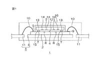
以下では、この発明の実施の形態を、添付図面を参照して詳細に説明する。
図1は、この発明の一実施形態に係る加速度センサの構成を示す図解的な断面図である。
加速度センサ1は、熱感知型の加速度センサである。この加速度センサ1は、発熱チップ2とセンサチップ3とを互いの表面を対向させた状態で接合した、チップ・オン・チップ構造を有している。
Hereinafter, embodiments of the present invention will be described in detail with reference to the accompanying drawings.
FIG. 1 is a schematic sectional view showing a configuration of an acceleration sensor according to an embodiment of the present invention.
The
発熱チップ2は、平面視略矩形状に形成されており、その表面4を上方に向けたフェイスアップ姿勢で、リードフレーム5のアイランド部6にダイボンディングされている。この発熱チップ2の表面4には、その中央部に、センサチップ3が接合される略矩形状のチップ接合領域が設定されている。
チップ接合領域には、複数の発熱チップ側バンプ7が、チップ接合領域の周縁に沿って互いに間隔を隔てて配置されている。各発熱チップ側バンプ7は、Au材料を用いて、表面4から突出して形成されている。さらに、チップ接合領域には、たとえば、4個の発熱素子としての抵抗素子8が作り込まれている。
The heat generating chip 2 is formed in a substantially rectangular shape in plan view, and is die-bonded to the
In the chip bonding area, a plurality of heat generating
また、発熱チップ2の表面4には、チップ接合領域を取り囲む周縁部に、複数の外部接続用パッド9が設けられている。この外部接続用パッド9は、ボンディングワイヤ10を介して、リードフレーム5のリード部11に電気的に接続(ワイヤボンディング)されている。
センサチップ3は、平面視において発熱チップ2よりも小さな略矩形状に形成されており、その表面12を下方に向けたフェイスダウン姿勢で、発熱チップ2の表面4のチップ接合領域に接合されている。
A plurality of external connection pads 9 are provided on the surface 4 of the heat generating chip 2 at the peripheral edge surrounding the chip bonding area. The external connection pads 9 are electrically connected (wire bonding) to the
The
センサチップ3の表面12には、複数のセンサチップ側バンプ13が、発熱チップ2の各発熱チップ側バンプ7と対向する位置に配置されている。各発熱チップ側バンプ7は、Au材料を用いて、表面12から突出して形成されている。さらに、センサチップ3の表面には、たとえば、16個の熱電対素子14が作り込まれている。
発熱チップ2とセンサチップ3とが接合された状態で、発熱チップ2の各発熱チップ側バンプ7とセンサチップ3の各センサチップ側バンプ13とは、互いに頂面を突き合わせて対向し、Sn材料からなる接続金属部15を挟んで接続されている。
On the
In a state where the heat generating chip 2 and the
発熱チップ2とセンサチップ3との接合前の状態において、センサチップ3の各センサチップ側バンプ13の頂面には、接続金属部15の材料であるSn材料が塗布されている。そして、発熱チップ2とセンサチップ3とが接合されて、発熱チップ2の各発熱チップ側バンプ7とセンサチップ3の各センサチップ側バンプ13とが突き合わされた状態で、熱処理が行われると、各センサチップ側バンプ13の頂面のSn材料が溶融する。これにより、各発熱チップ側バンプ7と各センサチップ側バンプ13との間に接続金属部15が形成され、この接続金属部15により各発熱チップ側バンプ7と各センサチップ側バンプ13とを確実に接続することができる。
In a state before the heat generating chip 2 and the
各発熱チップ側バンプ7と各センサチップ側バンプ13とが接続金属部15を介して接続されることにより、発熱チップ2およびセンサチップ3は、発熱チップ側バンプ7とセンサチップ側バンプ13とを接続金属部15で接続して形成される各バンプを介して、電気的に接続され、かつ、互いの間に所定間隔を保った状態で機械的に接続される。
そして、発熱チップ2およびセンサチップ3は、リードフレーム5およびボンディングワイヤ10とともに、樹脂パッケージ16により封止されている。リードフレーム5のリード部11の一部は、樹脂パッケージ16から露出し、プリント配線基板などとの外部接続部(アウターリード部)として機能する。
Each heat generating
The heat generating chip 2 and the
図2は、センサチップ3の表面12を示す平面図である。この図2において、発熱チップ2の各抵抗素子8がセンサチップ3の表面12に投影して示されている。また、図2では、センサチップ3のセンサチップ側バンプ13の図示が省略されている。
発熱チップ2の4個の抵抗素子8は、発熱チップ2の表面4において、チップ接合領域の中心に対してそのチップ接合領域の1辺に沿うX方向の両側にそれぞれ1個ずつ配置され、チップ接合領域の中心に対してX方向と直交するY方向の両側にそれぞれ1個ずつ配置されている。チップ接合領域の中心に対してX方向の両側に配置された各抵抗素子8は、チップ接合領域の中心からX方向に等間隔を隔てた位置でY方向に延びている。一方、チップ接合領域の中心に対してY方向の両側に配置された各抵抗素子8は、チップ接合領域の中心からY方向に等間隔を隔てた位置でX方向に延びている。
FIG. 2 is a plan view showing the
The four resistance elements 8 of the heat generating chip 2 are arranged one by one on the surface 4 of the heat generating chip 2 on both sides in the X direction along one side of the chip bonding area with respect to the center of the chip bonding area. One is arranged on each side of the Y direction perpendicular to the X direction with respect to the center of the bonding region. Each resistance element 8 disposed on both sides in the X direction with respect to the center of the chip bonding region extends in the Y direction at a position spaced equally from the center of the chip bonding region in the X direction. On the other hand, the resistance elements 8 arranged on both sides in the Y direction with respect to the center of the chip bonding area extend in the X direction at positions spaced equidistantly in the Y direction from the center of the chip bonding area.
センサチップ3の16個の熱電対素子14は、各抵抗素子8に4個ずつ対応づけられている。X方向に延びる各抵抗素子8に対応づけられた4個の熱電対素子14は、センサチップ3の表面12において、センサチップ3の表面12への各抵抗素子8の投影に対して、そのY方向の両側に互いに対称をなすように2個ずつ配置されている。また、Y方向に延びる各抵抗素子8に対応づけられた4個の熱電対素子14は、センサチップ3の表面12において、センサチップ3の表面12への各抵抗素子8の投影に対して、そのX方向の両側に互いに対称をなすように2個ずつ配置されている。
Fourteen
なお、以下では、X方向に延びる各抵抗素子8に対応づけられた4個の熱電対素子14において、抵抗素子8の投影に対してそのY方向に対称をなす2個の熱電対素子14の対を、単に「Y方向の熱電対素子14の対」という。また、Y方向に延びる各抵抗素子8に対応づけられた4個の熱電対素子14において、抵抗素子8の投影に対してそのX方向に対称をなす2個の熱電対素子14の対を、単に「X方向の熱電対素子14の対」という。
In the following, in the four
図3は、抵抗素子8からの熱放射の状態を説明するための図である。
発熱チップ2の各抵抗素子8に通電されると、各抵抗素子8からの発熱がセンサチップ3に向けてX方向およびY方向に均等に放射される。
Y方向の熱電対素子14の対は、センサチップ3の表面12への各抵抗素子8の投影に対してY方向に互いに対称に配置されているので、この加速度センサ1が静止している状態では、その対をなす各熱電対素子14により検出される温度の差は零である。また、X方向の熱電対素子14の対は、センサチップ3の表面12への各抵抗素子8の投影に対してX方向に互いに対称に配置されているので、この加速度センサ1が静止している状態では、その対をなす各熱電対素子14により検出される温度の差は零である。
FIG. 3 is a diagram for explaining the state of thermal radiation from the resistance element 8.
When each resistance element 8 of the heat generating chip 2 is energized, heat generated from each resistance element 8 is evenly radiated toward the
Since the pair of
そして、この加速度センサ1にX方向の加速度が加わると、図3に破線矢印で示すように、各抵抗素子8からの発熱の放射方向がX方向に偏る。そのため、X方向の熱電対素子14の対をなす各熱電対素子14により検出される温度に差が生じる。また、加速度センサ1にY方向の加速度が加わると、各抵抗素子8からの発熱の放射方向がY方向に偏る。そのため、Y方向の熱電対素子14の対をなす各熱電対素子14により検出される温度に差が生じる。したがって、X方向の熱電対素子14の各対およびY方向の熱電対素子14の各対により検出される温度の差に基づいて、この加速度センサ1に加わる加速度の方向および大きさを検出することができる。
When acceleration in the X direction is applied to the
なお、センサチップ3は、発熱チップ2の上方に配置されていることが好ましい。このような配置であれば、各抵抗素子8からの発熱が各熱電対素子14に良好に達するので、各抵抗素子8の発熱量の低減および/または各熱電対素子14の感度の向上を図ることができる。
以上のように、この加速度センサ1では、発熱チップ2の表面4に抵抗素子8が設けられ、センサチップ3の表面12に熱電対素子14が設けられて、それらの発熱チップ2とセンサチップ3とが各表面4,12を互いに対向させたフェースツーフェース状態で接合されている。このような構成の加速度センサ1の製造工程では、従来の熱感知型の加速度センサの製造工程で手間を要する工程(基板に凹部を形成したり、その凹部上にヒータや熱電対を架設したりする工程)を不要とすることができる。そのため、加速度センサ1は、その製造工程が簡素であり、低コストで製造することができる。
The
As described above, in the
また、発熱チップ2とセンサチップ3との間に、発熱チップ側バンプ7とセンサチップ側バンプ13とを接続金属部15で接続して形成されるバンプが介在されることにより、発熱チップ2とセンサチップ3との間隔を所定間隔に精度よく保持することができる。そのため、各熱電対素子14により各抵抗素子8からの熱放射の状態の変化を良好に検出することができ、この加速度センサ1に加えられる加速度を良好に検出することができる。
In addition, a bump formed by connecting the heat generating
さらにまた、発熱チップ2およびセンサチップ3が樹脂パッケージ16で封止されているので、各抵抗素子8からの熱放射の状態が樹脂パッケージ16の外部からの影響を受けて変化することを防止することができる。そのため、各熱電対素子14により抵抗素子8からの熱放射の状態の変化を良好に検出することができ、加速度センサ1に加えられる加速度をより良好に検出することができる。
Furthermore, since the heat generating chip 2 and the
以上、この発明の一実施形態を説明したが、この発明は他の形態で実施することもできる。たとえば、前述の実施形態では、発熱チップ2に4個の抵抗素子8が設けられている構成を例示したが、発熱チップ2に設けられる抵抗素子8の個数は、1〜3個であってもよいし、5個以上であってもよい。
また、各抵抗素子8に対応づけて4個の熱電対素子14が設けられている構成を例示したが、各抵抗素子8に対応づけて1個以上の熱電対素子14が設けられるとよい。
Although one embodiment of the present invention has been described above, the present invention can be implemented in other forms. For example, in the above-described embodiment, the configuration in which the four resistance elements 8 are provided in the heat generating chip 2 is illustrated, but the number of the resistance elements 8 provided in the heat generating chip 2 may be 1 to 3. It may be 5 or more.
Further, the configuration in which four
その他、特許請求の範囲に記載された事項の範囲で種々の設計変更を施すことが可能である。 In addition, various design changes can be made within the scope of matters described in the claims.
1 加速度センサ
2 発熱チップ
3 センサチップ
4 表面
7 発熱チップ側バンプ
8 抵抗素子
12 表面
13 センサチップ側バンプ
14 熱電対素子
15 接続金属部
16 樹脂パッケージ
DESCRIPTION OF
Claims (8)
表面に複数の熱電対素子が形成され、前記複数の熱電対素子が前記発熱素子と対向する位置を挟む両側に配置されるように、その表面を前記発熱チップの表面に対向させて配置されたセンサチップとを含み、
前記発熱素子から前記センサチップへ向けて放射された発熱を各前記熱電対素子で検出し、前記センサチップの前記表面における前記発熱素子と対向する位置に対して一方側の前記熱電対素子の検出値と、当該位置に対して他方側の前記熱電対素子の検出値との差に基づいて加速度の方向および大きさを検出することを特徴とする、加速度センサ。 A heating chip having a heating element formed on the surface;
A plurality of thermocouple elements are formed on the surface, and the plurality of thermocouple elements are disposed so as to be opposed to the surface of the heat generating chip so that the plurality of thermocouple elements are disposed on both sides of the position facing the heat generating element . and a sensor chip only contains,
Heat generation radiated from the heating element toward the sensor chip is detected by each thermocouple element, and detection of the thermocouple element on one side with respect to a position facing the heating element on the surface of the sensor chip An acceleration sensor that detects a direction and a magnitude of acceleration based on a difference between a value and a detected value of the thermocouple element on the other side with respect to the position .
前記発熱素子は、前記発熱チップの前記表面において、前記チップ接合領域の中心に対してそのチップ接合領域の1辺に沿う第1方向の両側にそれぞれ1個ずつ配置され、前記チップ接合領域の中心に対して前記第1方向と直交する第2方向の両側にそれぞれ1個ずつ配置された複数の発熱素子を含む、請求項1〜4のいずれか一項に記載の加速度センサ。 One heating element is disposed on each surface of the heating chip on each side in the first direction along one side of the chip bonding area with respect to the center of the chip bonding area, and the center of the chip bonding area The acceleration sensor according to any one of claims 1 to 4, further comprising a plurality of heating elements arranged one on each side in a second direction orthogonal to the first direction.
前記チップ接合領域の中心に対して前記第2方向の両側に配置された各前記発熱素子は、前記チップ接合領域の中心から前記第2方向に等間隔を隔てた位置で前記第1方向に延びている、請求項5に記載の加速度センサ。 Each of the heating elements disposed on both sides in the second direction with respect to the center of the chip bonding area extends in the first direction at a position equidistant from the center of the chip bonding area in the second direction. The acceleration sensor according to claim 5.
前記第2方向に延びる各前記発熱素子に対応づけられた4個の前記熱電対素子は、前記センサチップの前記表面において、前記センサチップの前記表面への各前記発熱素子の投影に対して、その前記第1方向の両側に互いに対称をなすように2個ずつ配置されている、請求項6に係る請求項7に記載の加速度センサ。 The four thermocouple elements associated with each of the heating elements extending in the second direction are projected on the surface of the sensor chip with respect to the projection of the heating elements on the surface of the sensor chip. The acceleration sensor according to claim 7 according to claim 6, wherein two acceleration sensors are arranged so as to be symmetrical to each other on both sides in the first direction.
Priority Applications (2)
| Application Number | Priority Date | Filing Date | Title |
|---|---|---|---|
| JP2006212352A JP4955334B2 (en) | 2006-08-03 | 2006-08-03 | Acceleration sensor |
| US11/833,061 US7735368B2 (en) | 2006-08-03 | 2007-08-02 | Acceleration sensor |
Applications Claiming Priority (1)
| Application Number | Priority Date | Filing Date | Title |
|---|---|---|---|
| JP2006212352A JP4955334B2 (en) | 2006-08-03 | 2006-08-03 | Acceleration sensor |
Publications (2)
| Publication Number | Publication Date |
|---|---|
| JP2008039519A JP2008039519A (en) | 2008-02-21 |
| JP4955334B2 true JP4955334B2 (en) | 2012-06-20 |
Family
ID=39174706
Family Applications (1)
| Application Number | Title | Priority Date | Filing Date |
|---|---|---|---|
| JP2006212352A Expired - Fee Related JP4955334B2 (en) | 2006-08-03 | 2006-08-03 | Acceleration sensor |
Country Status (2)
| Country | Link |
|---|---|
| US (1) | US7735368B2 (en) |
| JP (1) | JP4955334B2 (en) |
Families Citing this family (11)
| Publication number | Priority date | Publication date | Assignee | Title |
|---|---|---|---|---|
| US20090293618A1 (en) * | 2005-08-18 | 2009-12-03 | C & N Inc. | Acceleration Sensor Device |
| WO2007147137A2 (en) | 2006-06-15 | 2007-12-21 | Sitime Corporation | Stacked die package for mems resonator system |
| JP2008002837A (en) * | 2006-06-20 | 2008-01-10 | Denso Corp | Method of manufacturing semiconductor capacitive sensor |
| US8607631B2 (en) * | 2011-04-22 | 2013-12-17 | Texas Instruments Incorporated | Heated air mass WCSP package and method for accelerometer |
| US8686555B2 (en) * | 2011-06-29 | 2014-04-01 | Invensense, Inc. | Integrated heater on MEMS cap for wafer scale packaged MEMS sensors |
| JP5912958B2 (en) * | 2012-07-20 | 2016-04-27 | ルネサスエレクトロニクス株式会社 | Semiconductor device |
| JP5902305B2 (en) * | 2012-09-12 | 2016-04-13 | ルネサスエレクトロニクス株式会社 | Semiconductor device |
| US9560779B2 (en) * | 2014-10-02 | 2017-01-31 | Honeywell International Inc. | Thermal stabilization of temperature sensitive components |
| US10139124B2 (en) * | 2017-01-13 | 2018-11-27 | Lennox Industries Inc. | Method and apparatus for system diagnostics using accelerometers |
| US11302611B2 (en) | 2018-11-28 | 2022-04-12 | Texas Instruments Incorporated | Semiconductor package with top circuit and an IC with a gap over the IC |
| US11067322B2 (en) | 2019-01-30 | 2021-07-20 | Lennox Industries Inc. | Method and apparatus for preventing component malfunction using accelerometers |
Family Cites Families (25)
| Publication number | Priority date | Publication date | Assignee | Title |
|---|---|---|---|---|
| JPH0599942A (en) * | 1991-10-11 | 1993-04-23 | Nippon Steel Corp | Flow-velocity measuring apparatus using silicon |
| EP0664456B1 (en) * | 1994-01-20 | 1999-07-07 | Honda Giken Kogyo Kabushiki Kaisha | Acceleration sensor |
| US5786744A (en) * | 1994-03-24 | 1998-07-28 | Honda Giken Kogyo Kabushiki Kaisha | Hybrid sensor |
| US5581034A (en) * | 1995-01-13 | 1996-12-03 | Remec, Inc. | Convective accelerometer and inclinometer |
| US6182509B1 (en) * | 1996-06-26 | 2001-02-06 | Simon Fraser University | Accelerometer without proof mass |
| US6589433B2 (en) * | 1996-06-26 | 2003-07-08 | Simon Fraser University | Accelerometer without proof mass |
| JP3500040B2 (en) * | 1997-06-02 | 2004-02-23 | 株式会社リコー | Flow sensor |
| JP3846094B2 (en) * | 1998-03-17 | 2006-11-15 | 株式会社デンソー | Manufacturing method of semiconductor device |
| TW412817B (en) * | 1998-06-19 | 2000-11-21 | Matsushita Electric Ind Co Ltd | A bump bonding apparatus and method |
| JP2000193677A (en) | 1998-12-24 | 2000-07-14 | Mazda Motor Corp | Acceleration sensor |
| US6171880B1 (en) * | 1999-06-14 | 2001-01-09 | The United States Of America As Represented By The Secretary Of Commerce | Method of manufacture of convective accelerometers |
| US6750521B1 (en) * | 1999-10-22 | 2004-06-15 | Delphi Technologies, Inc. | Surface mount package for a micromachined device |
| JP2001227902A (en) * | 2000-02-16 | 2001-08-24 | Mitsubishi Electric Corp | Semiconductor device |
| EP2197120B1 (en) * | 2000-03-15 | 2012-07-25 | Hitachi Metals, Ltd. | High-frequency module and wireless communication device |
| JP4089152B2 (en) * | 2000-06-23 | 2008-05-28 | オムロン株式会社 | Heat generating device for sensor, sensor and acceleration sensor |
| US6795752B1 (en) * | 2000-11-03 | 2004-09-21 | Memsic, Inc. | Thermal convection accelerometer with closed-loop heater control |
| JP2003297874A (en) * | 2002-03-29 | 2003-10-17 | Nec Electronics Corp | Connection structure and connection method for electronic component |
| US6835593B2 (en) * | 2002-08-01 | 2004-12-28 | Rohm Co., Ltd. | Method for manufacturing semiconductor device |
| TW574128B (en) * | 2002-11-29 | 2004-02-01 | Lightuning Tech Inc | Thermal bubble type micro-machined inertial sensor |
| JP2004271312A (en) * | 2003-03-07 | 2004-09-30 | Denso Corp | Capacitance-type semiconductor sensor device |
| US7305881B2 (en) * | 2004-06-09 | 2007-12-11 | Memsic, Inc. | Method and circuitry for thermal accelerometer signal conditioning |
| US7392703B2 (en) | 2004-06-09 | 2008-07-01 | Memsic, Inc. | Z-axis thermal accelerometer |
| WO2006014065A1 (en) * | 2004-08-06 | 2006-02-09 | Hankuk Sensys Co,Ltd | A method and device for measuring acceleration and/or inclination by using thermal convention of a fluid |
| JP4754817B2 (en) * | 2004-12-20 | 2011-08-24 | Okiセミコンダクタ株式会社 | Semiconductor acceleration sensor |
| DE102005041452A1 (en) * | 2005-08-31 | 2007-03-15 | Infineon Technologies Ag | Three-dimensional integrated electronic component and production process has chips, wafers or films with active and passive electronic components in embedded or printed circuits in many interconnected planes |
-
2006
- 2006-08-03 JP JP2006212352A patent/JP4955334B2/en not_active Expired - Fee Related
-
2007
- 2007-08-02 US US11/833,061 patent/US7735368B2/en not_active Expired - Fee Related
Also Published As
| Publication number | Publication date |
|---|---|
| US20080250859A1 (en) | 2008-10-16 |
| JP2008039519A (en) | 2008-02-21 |
| US7735368B2 (en) | 2010-06-15 |
Similar Documents
| Publication | Publication Date | Title |
|---|---|---|
| JP4955334B2 (en) | Acceleration sensor | |
| KR101317727B1 (en) | Structure having chip mounted thereon and module provided with the structure | |
| JP2007035962A (en) | Semiconductor device | |
| JP6346279B2 (en) | Force detector | |
| JP5843850B2 (en) | Mechanical quantity measuring device, semiconductor device, peeling detection device and module | |
| KR100931702B1 (en) | Thermopile Flow Rate Sensor | |
| JP5143640B2 (en) | Die mounting stress shielding structure | |
| JP2004333133A (en) | Inertial force sensor | |
| US9964560B2 (en) | Transfer mold type sensor device | |
| WO2003063258A1 (en) | Semiconductor device | |
| JP2011180146A (en) | Semiconductor device | |
| CN101828435B (en) | Bump structure with multiple layers and method of manufacture | |
| JPH02302634A (en) | Temperature sensor for semiconductor integrated circuit | |
| JP5333641B2 (en) | Infrared temperature sensor, electronic device, and method of manufacturing infrared temperature sensor | |
| WO2014020648A1 (en) | Electronic device | |
| JP2020016465A (en) | Fluid sensor | |
| JP5445384B2 (en) | Air flow measurement device | |
| JP2008281351A (en) | Electronic device | |
| JP5033045B2 (en) | Semiconductor element mounting structure | |
| JP2007281292A (en) | Semiconductor device mounting structure | |
| JP5723739B2 (en) | MEMS sensor | |
| JPH07280832A (en) | Acceleration detector | |
| JP2010071817A (en) | Semiconductor sensor built-in package | |
| JP2008045908A (en) | Acceleration sensor, sensor chip, and its manufacturing method | |
| WO2021039028A1 (en) | Sensor device |
Legal Events
| Date | Code | Title | Description |
|---|---|---|---|
| A621 | Written request for application examination |
Free format text: JAPANESE INTERMEDIATE CODE: A621 Effective date: 20090722 |
|
| A977 | Report on retrieval |
Free format text: JAPANESE INTERMEDIATE CODE: A971007 Effective date: 20110721 |
|
| A131 | Notification of reasons for refusal |
Free format text: JAPANESE INTERMEDIATE CODE: A131 Effective date: 20110804 |
|
| A521 | Request for written amendment filed |
Free format text: JAPANESE INTERMEDIATE CODE: A523 Effective date: 20110930 |
|
| TRDD | Decision of grant or rejection written | ||
| A01 | Written decision to grant a patent or to grant a registration (utility model) |
Free format text: JAPANESE INTERMEDIATE CODE: A01 Effective date: 20120308 |
|
| A01 | Written decision to grant a patent or to grant a registration (utility model) |
Free format text: JAPANESE INTERMEDIATE CODE: A01 |
|
| A61 | First payment of annual fees (during grant procedure) |
Free format text: JAPANESE INTERMEDIATE CODE: A61 Effective date: 20120315 |
|
| R150 | Certificate of patent or registration of utility model |
Free format text: JAPANESE INTERMEDIATE CODE: R150 |
|
| FPAY | Renewal fee payment (event date is renewal date of database) |
Free format text: PAYMENT UNTIL: 20150323 Year of fee payment: 3 |
|
| LAPS | Cancellation because of no payment of annual fees |