JP4941289B2 - Jet solder bath - Google Patents
Jet solder bath Download PDFInfo
- Publication number
- JP4941289B2 JP4941289B2 JP2007501661A JP2007501661A JP4941289B2 JP 4941289 B2 JP4941289 B2 JP 4941289B2 JP 2007501661 A JP2007501661 A JP 2007501661A JP 2007501661 A JP2007501661 A JP 2007501661A JP 4941289 B2 JP4941289 B2 JP 4941289B2
- Authority
- JP
- Japan
- Prior art keywords
- duct
- jet
- molten solder
- solder
- nozzle
- Prior art date
- Legal status (The legal status is an assumption and is not a legal conclusion. Google has not performed a legal analysis and makes no representation as to the accuracy of the status listed.)
- Active
Links
- 229910000679 solder Inorganic materials 0.000 title claims description 173
- 238000005476 soldering Methods 0.000 description 11
- 239000010935 stainless steel Substances 0.000 description 8
- 229910001220 stainless steel Inorganic materials 0.000 description 8
- 230000003628 erosive effect Effects 0.000 description 6
- 239000000470 constituent Substances 0.000 description 3
- 230000000694 effects Effects 0.000 description 3
- 229910045601 alloy Inorganic materials 0.000 description 2
- 239000000956 alloy Substances 0.000 description 2
- 229910052759 nickel Inorganic materials 0.000 description 2
- 238000005275 alloying Methods 0.000 description 1
- 230000004888 barrier function Effects 0.000 description 1
- 230000000903 blocking effect Effects 0.000 description 1
- 238000001816 cooling Methods 0.000 description 1
- 230000007423 decrease Effects 0.000 description 1
- 230000005484 gravity Effects 0.000 description 1
- 238000002844 melting Methods 0.000 description 1
- 230000008018 melting Effects 0.000 description 1
- 239000002184 metal Substances 0.000 description 1
- 229910052751 metal Inorganic materials 0.000 description 1
- 238000000034 method Methods 0.000 description 1
- 238000002156 mixing Methods 0.000 description 1
- 238000003825 pressing Methods 0.000 description 1
- 230000000644 propagated effect Effects 0.000 description 1
- 230000001902 propagating effect Effects 0.000 description 1
Images


Classifications
-
- B—PERFORMING OPERATIONS; TRANSPORTING
- B23—MACHINE TOOLS; METAL-WORKING NOT OTHERWISE PROVIDED FOR
- B23K—SOLDERING OR UNSOLDERING; WELDING; CLADDING OR PLATING BY SOLDERING OR WELDING; CUTTING BY APPLYING HEAT LOCALLY, e.g. FLAME CUTTING; WORKING BY LASER BEAM
- B23K1/00—Soldering, e.g. brazing, or unsoldering
- B23K1/08—Soldering by means of dipping in molten solder
- B23K1/085—Wave soldering
-
- B—PERFORMING OPERATIONS; TRANSPORTING
- B23—MACHINE TOOLS; METAL-WORKING NOT OTHERWISE PROVIDED FOR
- B23K—SOLDERING OR UNSOLDERING; WELDING; CLADDING OR PLATING BY SOLDERING OR WELDING; CUTTING BY APPLYING HEAT LOCALLY, e.g. FLAME CUTTING; WORKING BY LASER BEAM
- B23K3/00—Tools, devices, or special appurtenances for soldering, e.g. brazing, or unsoldering, not specially adapted for particular methods
- B23K3/06—Solder feeding devices; Solder melting pans
- B23K3/0646—Solder baths
- B23K3/0653—Solder baths with wave generating means, e.g. nozzles, jets, fountains
Description
【技術分野】
【0001】
本発明は、溶融はんだを噴流させてプリント基板のはんだ付けを行う噴流はんだ槽に関する。
【背景技術】
【0002】
一般に、テレビ、ビデオのような家電製品に組み込むプリント基板は自動はんだ付け装置ではんだ付けが行われている。自動はんだ付け装置には、フラクサー、プリヒーター、噴流はんだ槽、冷却機等の処理装置が設置されており、プリント基板は、搬送装置で搬送されながらフラクサーでフラックス塗布、プリヒーターで予備加熱、噴流はんだ槽ではんだの付着、冷却機で冷却が行われて、はんだ付けがなされる。
【0003】
自動はんだ付け装置に設置された処理装置は、全てはんだ付けの良否に係わるものであるが、特に噴流はんだ槽はこれに最も影響している。即ち噴流はんだ槽は、噴流状態によりはんだ付け不良が発生したり、酸化物がプリント基板に付着したりする。また自動はんだ付け装置の処理装置は長期間安定して使用できるものであるが、噴流はんだ槽は他の処理装置よりも耐用期間が短い。
【0004】
噴流はんだ槽には、溶融はんだを荒れた状態で噴流する一次噴流ノズルと、溶融はんだを静かな状態で噴流する二次噴流ノズルが設置されている。一次噴流ノズルから噴流する溶融はんだは荒れているため、プリント基板のスルーホールや表面実装部品の隅部のように溶融はんだが侵入しにくい箇所に容易に侵入して未はんだをなくすものである。しかしながら溶融はんだが荒れていると、プリント基板に接触したときにはんだが隣接したはんだ付け部間に跨って付着するというブリッジや、リード先端にはんだが角状に付着するというツララが発生してしまう。そこで、これらブリッジやツララが発生したプリント基板を二次噴流ノズルから噴流する静かな溶融はんだに接触させることにより、ブリッジやツララを修正する。
【0005】
一次噴流ノズルの溶融はんだを荒らすことについては、従来より各種の方法・手段が提案され、それぞれ効果を発揮して未はんだをなくすことは或る程度解決されている。一方、二次噴流ノズルは、単に静かな噴流をさせるだけであるため、特別な手段は必要とされてなく問題はないとされていた。ここで従来の噴流はんだ槽の二次噴流ノズルについて説明する。図4は従来の噴流はんだ槽の二次噴流ノズルの正面断面図、図5は同一部破断斜視図、図6は同側面断面図である。
[0006]
噴流はんだ槽には、一次噴流ノズル(図示せず)と二次噴流ノズル21が設置されている。また噴流はんだ槽20には溶融はんだ22が入れられており、図示しない電熱ヒーターではんだの溶融を行うとともに、溶融したはんだを所定の温度に保つようになっている。二次噴流ノズル21は、ダクト23、インペラポンプ24、ノズル口25、整流板26から構成されている。
[0007]
ダクト23は、一端に約3/4円弧のポンプ室27が形成されており、該ポンプ室には噴流ポンプ24が設置されている。従来の噴流ノズルで多く使用されているインペラポンプは図4、5に示すように、多数の羽根28・・・が放射状に取り付けられたものである。インペラポンプ24の上部中央には軸29が固定されており、該軸の上端は図示しないモーターと連動している。ポンプ室27の下部には流入口30が開口している。
[0008]
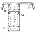
またダクト23の他端は、上方に立ち上がった係合部31となっている。従来の噴流はんだ槽における二次噴流ノズルのダクトは、図5に示すようにポンプ室27の出口が狭くなっており、係合部31に至る間が暫時巾広となっている。このようにポンプ室から係合部間のダクトの巾が暫時巾広となっているのは、インペラポンプはポンプ室の下部から流入した溶融はんだを多数の羽根で払い飛ばすものであり、ポンプ室内の圧力を高めてダクトに流出させるため、ポンプ室の出口を狭めてある。しかしながらダクト巾が狭いままであると、ノズル口に達する溶融はんだの量が少なくなることからポンプ室から係合部間のダクトを暫時巾広くしてある。また従来の噴流はんだ槽の二次噴流ノズルは、図6に示すようにノズル口の横巾(W3)とダクトの横巾(W4)とが同一となっている。
[0009]
係合部31にはノズル口25が密閉状態で係合されており、該係合部には多数の穴32・・・が穿設された整流板26が張設されている。ポンプ室から勢いよくダクト内に流出された溶融はんだは乱流となっており、そのまま二次噴流ノズルのノズル口から噴流させると、静かな噴流状態が得られなくなるため、この整流板で乱流を整流にする。乱流は整流板の多数の穴を通過するときに整流化され、ノズル口からは静かな状態で噴流されるようになる。また整流板は、乱流を整流化するばかりでなく、溶融はんだ中に混入した酸化物の除去作用も有している。噴流はんだ槽では、ノズル口近辺の溶融はんだ液面上に酸化物が浮遊しており、ノズル口から噴流した溶融はんだが溶融はんだの液面上に落下するときに、比重の軽い酸化物を巻き込んで酸化物が溶融はんだの下方に沈む。この下方に沈んだ酸化物は、溶融はんだを勢いよく吸い込むインペラポンプに吸い込まれてダクト内に入り、それがノズル口から溶融はんだとともに噴流してプリント基板に付着する。そこでダクト上部に整流板を設置して、整流板に酸化物を付着させ、酸化物が整流板から上方にいくのを止めるようにしている。
【0010】
ノズル口25には、プリント基板の進入側となるところにフロントフォーマー33が、そしてプリント基板の退出側となるところにはリヤフォーマー34が設置されている。フロントフォーマーは、ノズル口から噴流した溶融はんだを進入側に流すことにより、一次噴流ノズルで発生したブリッジやツララを再溶融させてなくすものである。しかし、そのままプリント基板が二次噴流ノズルから退出したのでは、はんだ付け部へのはんだの付着量が少なくなってしまうため、リヤフォーマーではんだを適量付着させるようになっている。つまりリヤフォーマーでは、溶融はんだがプリント基板の進行方向と同一方向でプリント基板の走行速度と略同一速度で流れているため、リヤフォーマーから流れる溶融はんだに接触したプリント基板には、適量のはんだが付着する。従来の噴流はんだ槽における二次噴流ノズルは、図6に示すようにダクトの横巾とノズル口の横巾が同一となっており、ダクト内に流入した溶融はんだが、そのまま上方に噴流されて静かな噴流状態を形成していたものである。
【0011】
続いて従来の噴流はんだ槽の二次噴流ノズルにおける噴流状態について説明する。図示しないモーターを駆動させて軸29を回転させることによりインペラポンプ24が回転する。するとインペラポンプ24の多数の羽根28・・・間にあった溶融はんだは該羽根で払い飛ばされてポンプ室27からダクト23内に流入していく。このときインペラポンプ24の羽根28・・・間に溶融はんだがなくなるため、ポンプ室27下部の流入口30から溶融はんだが勢いよくポンプ室27内に吸い込まれる。そしてダクト23内に流入した溶融はんだは、早い流速でダクトの先端に当たって図4の矢印で示すように流動方向を上方に変える。このとき溶融はんだは流速が早く、しかもダクト先端に当たって流動方向を変えたため乱流となっている。この乱流は、係合部31に張設された整流板26の多数の穴32・・・で整流化され、ノズル口25から上方に噴流される。図示しないプリント基板は、一次噴流ノズルではんだ付けされた後、二次噴流ノズルから噴流している溶融はんだに接触して、一次噴流ノズルで発生したブリッジやツララを修正するとともに、適量のはんだを付着させて二次噴流ノズルから退出する。
[0012]
従来の噴流はんだ槽に使用されていたポンプとしては、図4、5に示すインペラポンプが主流であったが、かつてはスパイラルポンプも提案されていた(特許文献1〜5)。
【特許文献1】
実公昭48−19425号公報
【特許文献2】
実開昭48−98520号公報
【特許文献3】
実開昭50−148327号公報
【特許文献4】
実開昭51−3632号公報
【特許文献5】
特開昭62−259665号公報
【発明の開示】
【発明が解決しようとする課題】
[0013]
ところで前述従来の噴流はんだ槽では、プリント基板全域にはんだが均一に付着しなかったり、プリント基板に酸化物が付着したり、さらには噴流はんだ槽を構成する部材が浸食されてしまったりすることがあった。また従来のスパイラルポンプを設置した噴流はんだ槽では、ノズル口から噴流する溶融はんだの噴流高さを充分に高くすることができなかったため、リヤフォーマーを流れる溶融はんだの速度調整ができず、適量のはんだを付着させることが困難であった。本発明は、従来の噴流はんだ槽における問題点に鑑み発明したもので、プリント基板全域にはんだを均一に付着させることができ、しかも酸化物の付着がないばかりでなく、噴流はんだ槽の構成部材の浸食もなく、さらにはノズル口から充分な溶融はんだを噴流させることができるという噴流はんだ槽を提供することにある。
【課題を解決するための手段】
[0014]
本発明者らは、従来の噴流はんだ槽における問題点について鋭意検討を加えた結果、従来の噴流はんだ槽の二次噴流ノズルにおいてプリント基板全域にはんだが均一に付着しない原因は、図4に示すように噴流高さが不均一、即ちダクト先端部の上方となるところの高さ(H1)が高く、ポンプ室に近いところの高さ(H2)が低くなるためである。図4の矢印で示すように、これは二次噴流ノズルにおいて、ダクト先端ではポンプ室から出た流速の早い溶融はんだ がダクト先端に勢いよく当たって流速の早いまま上方に流動するため高くなり、またポンプ室に近いところでは流速の早い溶融はんだのほとんどがダクトの先端方向に流動してポンプ室に近いところで上方に流動するのが少ないため低くなると考えられる。
【0015】
また従来の噴流はんだ槽でプリント基板に酸化物が付着するのは、インペラポンプが高速で回転してポンプ下部の溶融はんだを勢いよく吸い込むため、前述のように噴流後の溶融はんだに巻き込まれて下方に沈んでいた酸化物が溶融はんだとともにポンプ室に吸い込まれてしまう。そしてポンプ室に入った酸化物はダクトからノズル口に達してプリント基板に付着するようになる。従来の噴流はんだ槽の二次噴流ノズルには、整流板が設置されており、該整流板が穴の近辺に到来した酸化物を整流板に付着させて除去するだけであるため、完全に酸化物が除去できるほどの効果はなく、かえって穴の周囲に酸化物が堆積して大きくなってしまう。そしてこの大きくなった酸化物が整流板から離脱すると大きなった状態でプリント基板に付着してしまうことになる。従って噴流はんだ槽では、なるべく整流板を使わないことが望まれていた。
【0016】
また従来の噴流はんだ槽で、構成部材が浸食されるのは、やはりダクト内を流れる溶融はんだが早く流れるためである。つまり噴流はんだ槽の構成部材は、はんだが付着しにくいステンレスを用いているが、それでもステンレスは浸食されてしまう。ステンレスは、表面にNiやCrの強固な酸化物で覆われているため、該酸化物がバリヤーとなって溶融はんだを付着させないようになっている。ステンレスが溶融はんだに浸食されるのは、酸化物がなくなって清浄な金属面が現れたときにステンレス成分のFeやNiが溶融はんだ中のSnと合金化するからである。ステンレス成分がSnと合金化すると、合金の融点が下がるため、合金が溶融はんだ中に溶け込んでいく。そして合金化が徐々に広がるという浸食になり、ついには噴流はんだ槽の構成部材に穴が開いたり、構成部材が変形したりしてしまう。
[0017]
噴流はんだ槽において浸食、即ちステンレス表面の酸化物がなくなるのは、溶融はんだの流れが速かったり勢いよく当たったりして、溶融はんだによりステンレス表面が擦られて酸化物がなくなるからである。そのため噴流はんだ槽で浸食の発生しやすい部分は、図4に示すように、溶融はんだが勢いよくダクト内に流入するダクトの流入口A、溶融はんだを払い飛ばすインペラポンプの羽根B、溶融はんだが早く流れるダクトの狭い部分C、早い速度で溶融はんだが衝突するダクト先端D、溶融はんだが多数の穴を通過するときに穴が擦られる整流板E、等である。
[0018]
そこで本発明者らは、従来の噴流はんだ槽で発生する噴流高さの不均一、プリント基板への酸化物の付着、噴流はんだ槽の構成部材の浸食、等をなくすことについて鋭意研究を重ねた結果、溶融はんだがダクト内を流動するときの早い流れをなくすようにすればよいことに着目して本発明を完成させた。つまりダクト内では、溶融はんだを早く流すのではなく、ダクト内にある溶融はんだに対してダクトの一端から圧力をかけてダクト内の溶融はんだに圧力を伝搬させ、その伝搬による圧力でダクト他端のノズル口から溶融はんだを噴流させるようにする。
【0019】
本発明は、収容する溶融はんだを噴流する、少なくとも二次噴流ノズルを内部に配置する槽本体を備える噴流はんだ槽であって、二次噴流ノズルが、略水平方向へ延設されるとともに水平方向の一方の最端部の底部に溶融はんだが流入する入口を有するダクトと、このダクトの上部であって水平方向の他方の端部側にダクトに連通して上方向へ向けて延設され、上端部に溶融はんだが噴流する出口を有する係合部とにより構成され、ダクトが、槽本体の底部から上方に離間した位置にその底面が位置するように配置され、ダクトの内部の底部であってこのダクトの延設方向の一方の最端部には、入口に臨むとともに上端部及び下端部がいずれも開口したシリンダーがダクトの内部の天井部との間に隙間を有して設けられ、シリンダーの内部には螺旋状の羽根を四枚取り付けたスパイラルポンプが配置され、さらに、ダクトの延設方向と直交する水平方向に関する前記ダクトの距離が、該ダクトの延設方向と直交する水平方向に関する係合部の距離よりも大きいこと、および、スパイラルポンプの回転によってシリンダーの下部から溶融はんだが、シリンダーの内部に流入し、ダクトを通って噴流ノズルから噴流するようにしたことを特徴とする噴流はんだ槽である。
【発明の効果】
[0020]
本発明の噴流はんだ槽は、ダクトの一端に設置されたスパイラルポンプがダクト内の溶融はんだを勢いよく流すのではなく、例えば溶融はんだで圧力を伝搬させるような状態にし、溶融はんだが流れるとしても非常に遅い流速である。そのため本発明の噴流はんだ槽では、ダクトの一端の圧力がそのままダクト他端に設置されたノズル口まで伝搬され、ノズル口全体に同一の圧力がかかって、ノズル口からは高低差のない溶融はんだが噴流され、プリント基板に対しても溶融はんだが均一に接触して表面被りや未はんだを発生させない。
【0021】
また本発明の噴流はんだ槽は、溶融はんだをスパイラルポンプから噴流ノズルまで圧力伝播するようになっており、従来浸食が発生していた構成部材を強く擦ったり強く当たったりしないため、浸食が発生しない。
【0022】
さらにまた本発明の噴流はんだ槽は、シリンダーへの流入口が下向きとなっており、しかもシリンダー内への溶融はんだの吸い込みも緩やかであるため、酸化物の引き込まれが全くなく、従ってプリント基板への酸化物の付着もない。本来整流板は勢いのある流れを弱めて均一噴流にするとともに、整流板は酸化物の通過を阻止する役目も有しているものであるが、本発明の噴流はんだ槽では、前述のようにダクト内の溶融はんだの流れが遅く乱流とならないため整流化する必要がないばかりでなく、酸化物の混入もないため整流板を設置する必要もない。整流板は、酸化物を堆積させたり、溶融はんだに浸食されてはんだの成分を変えたりするため、できる限り使用したくないものであるが、本発明では、このように問題となる整流板を全く必要としないものである。
【発明を実施するための最良の形態】
【0023】
本発明の噴流はんだ槽に使用するスパイラルポンプとは、従来のインペラポンプのように吸い込みと吐き出しに急速な流れを起こすようなことがなく、溶融はんだに圧力をかけることができるものである。スパイラルポンプは、螺旋状となった羽根で溶融はんだを順次送り出すことにより溶融はんだに圧力をかけることができる。従来の噴流はんだ槽に使用されていたスパイラルポンプは、羽根が一枚設置されたものであるため、送り出す溶融はんだの量が少なかったり、脈流、即ちノズル口で溶融はんだが上下動したりすることがあった。スパイラルポンプの羽根の枚数を複数枚、好ましくは四枚にすると、送り出す量を多くすることができ、また円滑な流れを形成して脈流をなくす。本発明では、スパイラルポンプを上下に開口を有するシリンダー内に設置し、溶融はんだを下方から吸い込んで上方に圧力をかけるものであるため、溶融はんだが早く流動するようなことがない。またスパイラルポンプを下方から吸い込むようにしたため、溶融はんだの上方に浮遊している酸化物の吸い込みも全くない。
【0024】
本発明の噴流はんだ槽は、図3に示すようにノズル口の横巾W1がダクトの横巾W2よりも狭くなっている。このように噴流ノズルの横巾をダクトの横巾よりも狭くすることにより、ダクト内の大容量の溶融はんだの圧力がノズル内の小容量の溶融はんだに伝播するときに、パスカルの原理で噴流ノズル内には大量の溶融はんだが流入するため、噴流ノズルからは高い噴流が得られるようになる。
【0025】
以下図面に基づいて本発明噴流はんだ槽を説明する。図1は本発明噴流はんだ槽に設置する二次噴流ノズルの一部破断斜視図、図2は同正面断面図、図3は同側面断面図である。
【0026】
噴流はんだ槽1には一次噴流ノズル(図示せず)と二次噴流ノズル2が設置されている。噴流はんだ槽には溶融はんだ3が入れられており、図示しない電熱ヒーターではんだの溶融を行うとともに、溶融したはんだを所定の温度に保つようになっている。二次噴流ノズル2は、ダクト4、シリンダー5、スパイラルポンプ6、ノズル口7から構成されている。
【0027】
噴流はんだ槽1内には箱状のダクト4が設置されている。ダクト4の一端は半円筒状の圧力室8が形成されている。圧力室8の下部には、上下が開口となったシリンダー5が設置されている。シリンダー5の開口は、下部が流入口9、上部が加圧口10となっている。シリンダー5の高さは圧力室8の高さよりも低いものであり、シリンダー5の下部をダクト2の底面と同一レベルに置いてあるため、シリンダー5の上部と圧力室8の天井間は充分にあいている。
【0028】
シリンダー5内にはスパイラルポンプ6が設置されている。スパイラルポンプ6には四枚の螺旋状の羽根11・・・が取り付けられている。スパイラルポンプ6の上部中央には軸12が固定されており、該軸は圧力室8の天井を挿通して噴流はんだ槽1に入れられた溶融はんだ3の液面上まで突出している。軸12の上端は図示しないモーターと連動している。
【0029】
ダクト4の他端は細長い矩形の係合部13が立設している。該係合部にはノズル口7が密封状態で係合されている。また本発明の噴流はんだ槽は、図3に示すようにノズル口7の横巾W1がダクト4の横巾W2よりも小さくなっている。ノズル口7には、プリント基板の進入側となるところにフロントフォーマー14が、そしてプリント基板の退出側となるところにはリヤフォーマー15が設置されている。フロントフォーマーとリヤフォーマーの作用については前述の通りであるため説明は省略する。
[0030]
次に上記構造を有する本発明噴流はんだ槽での噴流状態について説明する。先ず図示しないモーターを駆動させて軸12を回転させると、シリンダー5内のスパイラルポンプ6が回転する。スパイラルポンプが回転すると、流入口9から溶融はんだが流入し、シリンダー内の溶融はんだが加圧口10から押し出されることにより、圧力室8内の溶融はんだ2に圧力がかかる。該圧力はダクト4内の溶融はんだに伝播され、さらにノズル口7内の溶融はんだまで伝播される。そのためノズル口7内の溶融はんだは上方に噴流されるようになる。上方に噴流された溶融はんだは、静かな噴流状態であり、フロントフォーマー14とリヤフォーマー15に沿って流れる。
[0031]
このときダクト内の溶融はんだは圧力を伝播する状態、即ち溶融はんだが移動するにしても流れが非常に遅い状態となっているため、溶融はんだが接触する構成部材を強く擦ったり強く当たったりすることがない。従って、本発明の噴流はんだ槽では浸食が発生しないものである。また本発明の噴流はんだ槽は、噴流ノズル近辺に浮遊していた酸化物が噴流後の溶融はんだに巻き込まれて溶融はんだ中の下方に沈んでも、スクリューポンプは下方の溶融はんだを急速に吸い込むものでないため、下方に沈んだ酸化物はダクト内に入り込むことがない。その結果、本発明の噴流はんだ槽では、はんだ付け時にプリント基板に酸化物が付着するような問題が発生しない。
【図面の簡単な説明】
[0032]
[図1]本発明噴流はんだ槽の正面断面図
[図2]本発明噴流はんだ槽に設置した二次噴流ノズルの一部破断斜視図
[図3]本発明噴流はんだ槽に設置した二次噴流ノズルの側面断面図
[図4]従来の噴流はんだ槽の正面断面図
[図5]従来の噴流はんだ槽に設置した二次噴流ノズルの一部破断斜視図
[図6]従来の噴流はんだ槽に設置した二次噴流ノズルの側面断面図
【符号の説明】
[0033]
1 噴流はんだ槽
2 二次噴流ノズル
3 溶融はんだ
4 ダクト
5 シリンダー
6 スパイラルポンプ
7 ノズル口
【産業上の利用可能性】
【0034】
本発明の実施例では、溶融はんだを静かに噴流する二次噴流ノズルについて説明したが、本発明は噴流する溶融はんだを荒らす一次噴流ノズルにも適応できることはいうまでもない。【Technical field】
[0001]
The present invention relates to a jet solder bath for soldering a printed circuit board by jetting molten solder.
[Background]
[0002]
In general, a printed circuit board to be incorporated in a home appliance such as a television or a video is soldered by an automatic soldering apparatus. The automatic soldering equipment is equipped with processing equipment such as a fluxer, preheater, jet solder bath, and cooler. The printed circuit board is fluxed by the fluxer while being transported by the transport device, preheated by the preheater, and jetted. Solder is attached by solder adhesion in a solder bath and cooling by a cooler.
[0003]
The processing devices installed in the automatic soldering apparatus are all related to the quality of soldering, but particularly the jet solder bath has the most influence on this. That is, in the jet solder bath, poor soldering occurs due to the jet state, or oxide adheres to the printed circuit board. Moreover, although the processing apparatus of an automatic soldering apparatus can be used stably for a long period of time, the jet solder bath has a shorter service life than other processing apparatuses.
[0004]
In the jet solder tank, a primary jet nozzle that jets molten solder in a rough state and a secondary jet nozzle that jets molten solder in a quiet state are installed. Since the molten solder jetted from the primary jet nozzle is rough, it easily penetrates into places where molten solder does not easily penetrate, such as through-holes of printed circuit boards and corners of surface-mounted components, thereby eliminating unsolder. However, when the molten solder is rough, a bridge in which the solder adheres across adjacent soldering portions when contacting the printed circuit board, and a wiggle in which the solder adheres in a square shape to the tip of the lead are generated. Therefore, the bridge and tsura are corrected by bringing the printed circuit board on which these bridges and tsura are generated into contact with a quiet molten solder jetted from the secondary jet nozzle.
[0005]
Various methods / means have been proposed for roughing the molten solder of the primary jet nozzle, and each effect has been solved to some extent. On the other hand, since the secondary jet nozzle merely causes a quiet jet, no special means is required and there is no problem. Here, a secondary jet nozzle of a conventional jet solder bath will be described. 4 is a front sectional view of a secondary jet nozzle of a conventional jet solder bath, FIG. 5 is a cutaway perspective view of the same part, and FIG. 6 is a side sectional view of the same.
[0006]
A primary jet nozzle (not shown) and a
[0007]
The
[0008]
The other end of the
[0009]
A
[0010]
The
[0011]
Then, the jet state in the secondary jet nozzle of the conventional jet solder tank is demonstrated. By driving a motor (not shown) to rotate the
[0012]
As the pump used in the conventional jet solder bath, the impeller pump shown in FIGS. 4 and 5 has been the mainstream, but in the past, spiral pumps have also been proposed (
[Patent Document 1]
Japanese Utility Model Publication No. 48-19425 [Patent Document 2]
Japanese Utility Model Publication No. 48-98520 [Patent Document 3]
Japanese Utility Model Publication No. 50-148327 [Patent Document 4]
Japanese Utility Model Publication No. 51-3632 [Patent Document 5]
JP 62-259665 A [Disclosure of the Invention]
[Problems to be solved by the invention]
[0013]
By the way, in the conventional jet solder bath, solder may not uniformly adhere to the entire printed circuit board, oxide may adhere to the printed circuit board, or the members constituting the jet solder bath may be eroded. there were. Also, in the conventional soldering bath equipped with a spiral pump, the height of the molten solder jetted from the nozzle port could not be sufficiently increased, so the speed of the molten solder flowing through the rear former could not be adjusted, and an appropriate amount of solder was required. It was difficult to adhere. The present invention was invented in view of the problems in the conventional jet solder bath, and can uniformly apply solder to the entire printed circuit board, and also has no oxide adhesion, and is a constituent member of the jet solder bath. It is another object of the present invention to provide a jet solder bath that can erode a sufficient amount of molten solder from the nozzle opening.
[Means for Solving the Problems]
[0014]
As a result of earnestly examining the problems in the conventional jet solder bath, the present inventors have shown in FIG. 4 the reason why the solder does not uniformly adhere to the entire printed circuit board in the secondary jet nozzle of the conventional jet solder bath. This is because the height of the jet flow is uneven, that is, the height (H 1 ) at the top of the duct tip is high and the height (H 2 ) near the pump chamber is low. As indicated by the arrow in FIG. 4, this is high in the secondary jet nozzle because the molten solder with a high flow velocity coming out of the pump chamber at the tip of the duct strikes the tip of the duct and flows upward with a high flow velocity. Further, it is considered that the molten solder having a high flow velocity near the pump chamber flows in the direction of the end of the duct and hardly flows upward near the pump chamber, so that it becomes low.
[0015]
Also, oxides adhere to the printed circuit board in the conventional jet solder bath because the impeller pump rotates at a high speed and sucks in the molten solder at the bottom of the pump vigorously. The oxide that has sunk downward is sucked into the pump chamber together with the molten solder. The oxide entering the pump chamber reaches the nozzle opening from the duct and adheres to the printed circuit board. The secondary jet nozzle of the conventional jet solder bath is equipped with a rectifying plate, and the rectifying plate only attaches to the rectifying plate and removes the oxide that has arrived in the vicinity of the hole. There is no effect to remove the object, and instead oxide is deposited around the hole and becomes large. And if this enlarged oxide leaves | separates from a baffle plate, it will adhere to a printed circuit board in a big state. Therefore, it has been desired that the jet solder bath should not use a current plate as much as possible.
[0016]
The reason why the component members are eroded in the conventional jet solder bath is that the molten solder flowing in the duct also flows quickly. That is, although the component member of the jet solder bath uses stainless steel to which solder is difficult to adhere, the stainless steel is still eroded. Since stainless steel has a surface covered with a strong oxide of Ni or Cr, the oxide serves as a barrier so that molten solder does not adhere. The reason why the stainless steel is eroded by the molten solder is that when the oxide disappears and a clean metal surface appears, the stainless steel component Fe or Ni is alloyed with Sn in the molten solder. When the stainless steel component is alloyed with Sn, the melting point of the alloy is lowered, so that the alloy is dissolved in the molten solder. And it becomes erosion that alloying spreads gradually, and finally a hole is opened in a constituent member of a jet solder tub, or a constituent member will change.
[0017]
The reason why the erosion, that is, the oxide on the surface of the stainless steel disappears in the jet solder bath is that the flow of the molten solder hits quickly or vigorously, and the surface of the stainless steel is rubbed by the molten solder and the oxide disappears. Therefore, as shown in FIG. 4, the portion where the erosion is likely to occur in the jet solder bath is as follows. A narrow portion C of the duct that flows fast, a duct tip D where the molten solder collides at a high speed, a current plate E that the holes are rubbed when the molten solder passes through a large number of holes, and the like.
[0018]
Therefore, the present inventors have conducted extensive research on eliminating the unevenness of the jet height generated in the conventional jet solder bath, the adhesion of oxide to the printed circuit board, the erosion of the components of the jet solder bath, and the like. As a result, the present invention has been completed by paying attention to the fact that it is only necessary to eliminate the fast flow when the molten solder flows in the duct. In other words, in the duct, instead of flowing the molten solder quickly, pressure is applied to the molten solder in the duct from one end of the duct to propagate the pressure to the molten solder in the duct, and the other end of the duct is caused by the pressure generated by the propagation. The molten solder is jetted from the nozzle opening.
[0019]
The present invention is a jet solder tank provided with a tank body in which at least a secondary jet nozzle is arranged to jet molten solder to be accommodated therein, and the secondary jet nozzle extends in a substantially horizontal direction and extends in the horizontal direction. A duct having an inlet through which molten solder flows in at the bottom of one of the ends of the first, and the upper part of the duct is connected to the duct at the other end in the horizontal direction and extends upward. And an engaging portion having an outlet through which molten solder spouts at the upper end, and the duct is disposed such that its bottom surface is located at a position spaced upward from the bottom of the tank body. One end of the duct extending in the extending direction is provided with a cylinder facing the entrance and having both an upper end and a lower end opened with a gap between the duct and the ceiling. Inside the cylinder A spiral pump having four spiral blades is arranged, and the distance of the duct with respect to the horizontal direction perpendicular to the duct extending direction is such that the engaging portion in the horizontal direction perpendicular to the duct extending direction is It is a jet solder bath characterized in that it is larger than the distance , and molten solder flows into the cylinder from the bottom of the cylinder by the rotation of the spiral pump, and jets from the jet nozzle through the duct. .
【Effect of the invention】
[0020]
In the jet solder bath of the present invention, the spiral pump installed at one end of the duct does not force the molten solder in the duct to flow vigorously. Very slow flow rate. Therefore, in the jet solder bath of the present invention, the pressure at one end of the duct is directly propagated to the nozzle port installed at the other end of the duct, the same pressure is applied to the entire nozzle port, and there is no difference in height from the nozzle port. The molten solder contacts the printed circuit board evenly and does not generate surface covering or unsolder.
[0021]
In addition, the jet solder tank of the present invention is adapted to propagate the pressure of the molten solder from the spiral pump to the jet nozzle, and does not rub against the components that have been eroded so far, so that no erosion occurs. .
[0022]
Furthermore, in the jet solder bath of the present invention, the inlet to the cylinder faces downward, and the suction of the molten solder into the cylinder is gentle, so that no oxide is drawn in, and therefore to the printed circuit board. There is no adhesion of oxide. Originally, the rectifying plate weakens the vigorous flow to make a uniform jet, and the rectifying plate also has the role of blocking the passage of oxides. Since the flow of the molten solder in the duct is slow and does not become turbulent, it is not necessary to rectify, and it is not necessary to install a rectifying plate because there is no mixing of oxides. The current plate is not desired to be used as much as possible because it deposits oxides or changes the components of the solder by being eroded by the molten solder. It is not necessary at all.
BEST MODE FOR CARRYING OUT THE INVENTION
[0023]
The spiral pump used in the jet solder bath of the present invention is capable of applying pressure to the molten solder without causing a rapid flow in suction and discharge unlike a conventional impeller pump. The spiral pump can apply pressure to the molten solder by sequentially feeding the molten solder with spiral blades. Since the spiral pump used in the conventional jet solder bath has one blade, the amount of molten solder to be sent out is small or the molten solder moves up and down at the pulsating flow, that is, at the nozzle port. There was a thing. When the number of blades of the spiral pump is plural, preferably four, the amount to be sent out can be increased, and a smooth flow is formed to eliminate the pulsating flow. In the present invention, the spiral pump is installed in a cylinder having openings up and down, and the molten solder is sucked from below and pressure is applied upward, so that the molten solder does not flow quickly. In addition, since the spiral pump is sucked from below, there is no suction of oxide floating above the molten solder.
[0024]
In the jet solder bath of the present invention, the lateral width W1 of the nozzle opening is narrower than the lateral width W2 of the duct, as shown in FIG. By making the width of the jet nozzle narrower than the width of the duct in this way, when the pressure of the large volume molten solder in the duct propagates to the small volume molten solder in the nozzle, the jet flow is based on the Pascal principle. Since a large amount of molten solder flows into the nozzle, a high jet flow can be obtained from the jet nozzle.
[0025]
The jet solder bath of the present invention will be described below with reference to the drawings. FIG. 1 is a partially broken perspective view of a secondary jet nozzle installed in a jet solder bath of the present invention, FIG. 2 is a front sectional view thereof, and FIG. 3 is a side sectional view thereof.
[0026]
The
[0027]
A box-shaped
[0028]
A
[0029]
At the other end of the
[0030]
Next, the jet state in the jet solder bath of the present invention having the above structure will be described. First, when a motor (not shown) is driven to rotate the
[0031]
At this time, the molten solder in the duct is in a state of propagating pressure, that is, the flow is very slow even if the molten solder moves, so that the component contacted by the molten solder is strongly rubbed or hit strongly. There is nothing. Therefore, erosion does not occur in the jet solder bath of the present invention. Moreover, the jet solder bath of the present invention is a screw pump in which the screw pump rapidly sucks the molten solder below even if the oxide floating near the jet nozzle is caught in the molten solder after the jet and sinks downward in the molten solder. Therefore, the oxide that sinks downward does not enter the duct. As a result, in the jet solder bath of the present invention, there is no problem that oxides adhere to the printed circuit board during soldering.
[Brief description of the drawings]
[0032]
[FIG. 1] Front sectional view of the jet solder bath of the present invention [FIG. 2] Partially broken perspective view of the secondary jet nozzle installed in the jet solder bath of the present invention [FIG. 3] Secondary jet installed in the jet solder bath of the present invention Side sectional view of nozzle [FIG. 4] Front sectional view of conventional jet solder bath [FIG. 5] Partially broken perspective view of secondary jet nozzle installed in conventional jet solder bath [FIG. 6] In conventional jet solder bath Side sectional view of the installed secondary jet nozzle [Explanation of symbols]
[0033]
1
[0034]
In the embodiments of the present invention, the secondary jet nozzle that gently jets the molten solder has been described, but it goes without saying that the present invention can also be applied to a primary jet nozzle that roughens the molten solder that jets.
Claims (1)
前記二次噴流ノズルは、略水平方向へ延設されるとともに水平方向の一方の最端部の底部に溶融はんだが流入する入口を有するダクトと、該ダクトの上部であって前記水平方向の他方の端部側に前記ダクトに連通して上方向へ向けて延設され、上端部に溶融はんだが噴流する出口を有する係合部とにより構成され、
前記ダクトは、前記槽本体の底部から上方に離間した位置にその底面が位置するように配置され、
前記ダクトの内部の底部であって当該ダクトの延設方向の前記一方の最端部には、前記入口に臨むとともに上端部及び下端部がいずれも開口したシリンダーが該ダクトの内部の天井部との間に隙間を有して設けられ、
該シリンダーの内部には螺旋状の羽根を四枚取り付けたスパイラルポンプが配置され、さらに、
前記ダクトの延設方向と直交する水平方向に関する前記ダクトの距離は、該ダクトの延設方向と直交する水平方向に関する前記係合部の距離よりも大きいこと、および
前記スパイラルポンプの回転によって前記シリンダーの下部から溶融はんだが、前記シリンダーの内部に流入し、前記ダクトを通って前記噴流ノズルから噴流するようにしたこと
を特徴とする噴流はんだ槽。A jet solder bath provided with a bath main body in which at least a secondary jet nozzle is arranged to jet a molten solder to be accommodated,
The secondary jet nozzle extends in a substantially horizontal direction and has a duct having an inlet through which molten solder flows into the bottom of one end in the horizontal direction and the other in the horizontal direction at the top of the duct. An end portion of which is connected to the duct and extends upward, and an engagement portion having an outlet through which molten solder is jetted at the upper end portion,
The duct is arranged such that its bottom surface is located at a position spaced upward from the bottom of the tank body,
A cylinder that is at the bottom of the duct and at the one end in the extending direction of the duct has a cylinder that faces the inlet and has both an upper end and a lower end that are open to the ceiling of the duct. Provided with a gap between
Inside the cylinder is arranged a spiral pump with four spiral blades attached,
The distance of the duct in the horizontal direction orthogonal to the extending direction of the duct is greater than the distance of the engaging portion in the horizontal direction orthogonal to the extending direction of the duct ; and
A jet solder bath , wherein molten solder flows into the inside of the cylinder by the rotation of the spiral pump, and jets from the jet nozzle through the duct .
Priority Applications (1)
| Application Number | Priority Date | Filing Date | Title |
|---|---|---|---|
| JP2007501661A JP4941289B2 (en) | 2005-02-07 | 2006-02-06 | Jet solder bath |
Applications Claiming Priority (4)
| Application Number | Priority Date | Filing Date | Title |
|---|---|---|---|
| JP2005030957 | 2005-02-07 | ||
| JP2005030957 | 2005-02-07 | ||
| PCT/JP2006/301976 WO2006082960A1 (en) | 2005-02-07 | 2006-02-06 | Jet solder bath |
| JP2007501661A JP4941289B2 (en) | 2005-02-07 | 2006-02-06 | Jet solder bath |
Publications (2)
| Publication Number | Publication Date |
|---|---|
| JPWO2006082960A1 JPWO2006082960A1 (en) | 2008-08-07 |
| JP4941289B2 true JP4941289B2 (en) | 2012-05-30 |
Family
ID=36777337
Family Applications (1)
| Application Number | Title | Priority Date | Filing Date |
|---|---|---|---|
| JP2007501661A Active JP4941289B2 (en) | 2005-02-07 | 2006-02-06 | Jet solder bath |
Country Status (7)
| Country | Link |
|---|---|
| US (1) | US8091758B2 (en) |
| EP (1) | EP1850646B1 (en) |
| JP (1) | JP4941289B2 (en) |
| CN (1) | CN101112139B (en) |
| DE (1) | DE602006015776D1 (en) |
| PL (1) | PL1850646T3 (en) |
| WO (1) | WO2006082960A1 (en) |
Families Citing this family (13)
| Publication number | Priority date | Publication date | Assignee | Title |
|---|---|---|---|---|
| JP5884058B2 (en) * | 2010-02-26 | 2016-03-15 | パナソニックIpマネジメント株式会社 | Soldering device |
| KR20130059760A (en) * | 2011-11-29 | 2013-06-07 | 삼성전기주식회사 | Apparatus for forming solder bump, and facility with the same |
| JP5601342B2 (en) | 2012-04-27 | 2014-10-08 | 千住金属工業株式会社 | Drift plate and jet device |
| DE102012013209A1 (en) * | 2012-07-04 | 2014-01-09 | Erwin Quarder Systemtechnik Gmbh | Soldering nozzle for soldering device for soldering components having a number of solder joints to be soldered, comprises nozzle chamber and a device with which solder flow in flow area and contour of exiting soldering wave is influenced |
| TWM454066U (en) * | 2013-01-25 | 2013-05-21 | Inventec Corp | Automatic welding equipment |
| DE102014211807A1 (en) * | 2014-06-20 | 2015-12-24 | Robert Bosch Gmbh | Soldering device and method for soldering |
| US9370838B2 (en) * | 2014-08-21 | 2016-06-21 | Illinois Tool Works Inc. | Wave soldering nozzle system and method of wave soldering |
| DE102016124642B4 (en) | 2016-12-16 | 2023-10-05 | Seho Vermögensverwaltungs Gmbh & Co. Kg | Method and device for soldering assemblies |
| CN109719361A (en) * | 2017-10-31 | 2019-05-07 | 康普技术有限责任公司 | The device and method that selective wave soldering connects |
| US20190366460A1 (en) * | 2018-06-01 | 2019-12-05 | Progress Y&Y Corp. | Soldering apparatus and solder nozzle module thereof |
| US10780516B2 (en) | 2018-06-14 | 2020-09-22 | Illinois Tool Works Inc. | Wave solder nozzle with automated adjustable sliding plate to vary solder wave width |
| JP6590232B1 (en) * | 2019-04-22 | 2019-10-16 | 千住金属工業株式会社 | Soldering apparatus and soldering method |
| US11389888B2 (en) | 2020-08-17 | 2022-07-19 | Illinois Tool Works Inc. | Wave solder nozzle with automated exit wing |
Citations (2)
| Publication number | Priority date | Publication date | Assignee | Title |
|---|---|---|---|---|
| JP2003053529A (en) * | 2001-08-07 | 2003-02-26 | Senju Metal Ind Co Ltd | Method of separating oxide and separator for oxide |
| JP2005028446A (en) * | 2003-06-17 | 2005-02-03 | Ktt:Kk | Pump for soldering tank and soldering tank using the same |
Family Cites Families (12)
| Publication number | Priority date | Publication date | Assignee | Title |
|---|---|---|---|---|
| US3752383A (en) * | 1971-11-11 | 1973-08-14 | Technical Devices Co | Soldering apparatus |
| JPS521771B2 (en) | 1972-03-25 | 1977-01-18 | ||
| DE2515437A1 (en) | 1974-04-16 | 1975-11-20 | Ici Ltd | PROCESS FOR THE CRYSTALLIZATION OF BIS (4-CHLOROPHENYL) SULPHONE |
| JPS513632A (en) | 1974-06-28 | 1976-01-13 | Kenkoo Kk | INGAYAKITSUKEHO |
| JPS62259665A (en) | 1986-01-20 | 1987-11-12 | Asahi Chem Res Lab Ltd | Method and device for injecting molten solder |
| JPS6471572A (en) * | 1987-09-09 | 1989-03-16 | Tamura Seisakusho Kk | Method for separating solder oxide |
| JPH0619968A (en) | 1991-09-13 | 1994-01-28 | Oki Electric Ind Co Ltd | Automatic extraction device for technical term |
| FR2682903B1 (en) * | 1991-10-28 | 1994-01-21 | Jacqueline Brizais | WAVE HEIGHT CONTROL DEVICE IN A WAVE WELDING INSTALLATION. |
| JPH0619968U (en) * | 1992-08-20 | 1994-03-15 | 株式会社コウキテクノ | Jet solder bath |
| JP2004009127A (en) * | 2002-06-11 | 2004-01-15 | Senju Metal Ind Co Ltd | Jet soldering bath |
| PL1676662T3 (en) * | 2003-10-10 | 2010-10-29 | Senju Metal Industry Co | Jet solder vessel |
| DE102004040405B4 (en) | 2004-08-19 | 2008-11-13 | Nec Europe Ltd. | Method for optimizing the energy consumption of a station in a wireless network |
-
2006
- 2006-02-06 EP EP06713119A patent/EP1850646B1/en active Active
- 2006-02-06 JP JP2007501661A patent/JP4941289B2/en active Active
- 2006-02-06 PL PL06713119T patent/PL1850646T3/en unknown
- 2006-02-06 US US11/883,846 patent/US8091758B2/en active Active
- 2006-02-06 DE DE602006015776T patent/DE602006015776D1/en active Active
- 2006-02-06 WO PCT/JP2006/301976 patent/WO2006082960A1/en active Search and Examination
- 2006-02-06 CN CN2006800035682A patent/CN101112139B/en active Active
Patent Citations (2)
| Publication number | Priority date | Publication date | Assignee | Title |
|---|---|---|---|---|
| JP2003053529A (en) * | 2001-08-07 | 2003-02-26 | Senju Metal Ind Co Ltd | Method of separating oxide and separator for oxide |
| JP2005028446A (en) * | 2003-06-17 | 2005-02-03 | Ktt:Kk | Pump for soldering tank and soldering tank using the same |
Also Published As
| Publication number | Publication date |
|---|---|
| WO2006082960A1 (en) | 2006-08-10 |
| EP1850646B1 (en) | 2010-07-28 |
| CN101112139B (en) | 2012-01-25 |
| US20100163599A1 (en) | 2010-07-01 |
| EP1850646A4 (en) | 2009-04-08 |
| CN101112139A (en) | 2008-01-23 |
| US8091758B2 (en) | 2012-01-10 |
| DE602006015776D1 (en) | 2010-09-09 |
| PL1850646T3 (en) | 2011-01-31 |
| JPWO2006082960A1 (en) | 2008-08-07 |
| EP1850646A1 (en) | 2007-10-31 |
Similar Documents
| Publication | Publication Date | Title |
|---|---|---|
| JP4941289B2 (en) | Jet solder bath | |
| JP4720905B2 (en) | Jet solder bath | |
| JP4253374B2 (en) | Method for soldering printed circuit board and jet solder bath | |
| JP4636085B2 (en) | Jet solder bath | |
| JP4605222B2 (en) | Jet solder bath | |
| JP2014114484A (en) | Snout floating scum removal device for molten zinc plating line | |
| JP2005171361A (en) | Apparatus for removing foreign substance on inner bath surface of snout in hot dip metal coating | |
| JP2003053529A (en) | Method of separating oxide and separator for oxide | |
| JP6007764B2 (en) | Floating scum removal device in snout in hot dip galvanizing line | |
| JP2003332724A (en) | Solder wave forming apparatus | |
| JP5391500B2 (en) | Soldering nozzle and soldering device | |
| JP4855166B2 (en) | Method for producing hot-dip galvanized steel sheet with a clean appearance | |
| JP2003205363A (en) | Soldering jet wave forming device by induction type electromagnetic pump system | |
| JP2006055904A (en) | Jet solder tank | |
| JP2010131667A (en) | Flow soldering apparatus | |
| JP3441527B2 (en) | Jet solder bath | |
| JP2000323826A (en) | Jet flow solder bath | |
| JPH0563349A (en) | Jet solder tank | |
| JP2002134898A (en) | Soldering method of printed board and jet solder tank | |
| JP2000340940A (en) | Wave soldering device | |
| JP2008043960A (en) | Jet nozzle for point soldering and its soldering equipment | |
| JPH0593653U (en) | Jet solder bath | |
| JP2002134897A (en) | Soldering method of printed board and jet solder tank | |
| JP2010229530A (en) | Method for removing dross floating in snout | |
| JP2005286265A (en) | Flow soldering apparatus |
Legal Events
| Date | Code | Title | Description |
|---|---|---|---|
| A621 | Written request for application examination |
Free format text: JAPANESE INTERMEDIATE CODE: A621 Effective date: 20080819 |
|
| A131 | Notification of reasons for refusal |
Free format text: JAPANESE INTERMEDIATE CODE: A131 Effective date: 20110628 |
|
| A521 | Request for written amendment filed |
Free format text: JAPANESE INTERMEDIATE CODE: A523 Effective date: 20110826 |
|
| TRDD | Decision of grant or rejection written | ||
| A01 | Written decision to grant a patent or to grant a registration (utility model) |
Free format text: JAPANESE INTERMEDIATE CODE: A01 Effective date: 20120131 |
|
| A01 | Written decision to grant a patent or to grant a registration (utility model) |
Free format text: JAPANESE INTERMEDIATE CODE: A01 |
|
| A61 | First payment of annual fees (during grant procedure) |
Free format text: JAPANESE INTERMEDIATE CODE: A61 Effective date: 20120213 |
|
| R150 | Certificate of patent or registration of utility model |
Ref document number: 4941289 Country of ref document: JP Free format text: JAPANESE INTERMEDIATE CODE: R150 Free format text: JAPANESE INTERMEDIATE CODE: R150 |
|
| FPAY | Renewal fee payment (event date is renewal date of database) |
Free format text: PAYMENT UNTIL: 20150309 Year of fee payment: 3 |
|
| FPAY | Renewal fee payment (event date is renewal date of database) |
Free format text: PAYMENT UNTIL: 20150309 Year of fee payment: 3 |
|
| R250 | Receipt of annual fees |
Free format text: JAPANESE INTERMEDIATE CODE: R250 |
|
| R250 | Receipt of annual fees |
Free format text: JAPANESE INTERMEDIATE CODE: R250 |
|
| R250 | Receipt of annual fees |
Free format text: JAPANESE INTERMEDIATE CODE: R250 |
|
| R250 | Receipt of annual fees |
Free format text: JAPANESE INTERMEDIATE CODE: R250 |
|
| R250 | Receipt of annual fees |
Free format text: JAPANESE INTERMEDIATE CODE: R250 |
|
| R250 | Receipt of annual fees |
Free format text: JAPANESE INTERMEDIATE CODE: R250 |
|
| R250 | Receipt of annual fees |
Free format text: JAPANESE INTERMEDIATE CODE: R250 |
|
| R250 | Receipt of annual fees |
Free format text: JAPANESE INTERMEDIATE CODE: R250 |
|
| R250 | Receipt of annual fees |
Free format text: JAPANESE INTERMEDIATE CODE: R250 |
|
| R250 | Receipt of annual fees |
Free format text: JAPANESE INTERMEDIATE CODE: R250 |