JP4939187B2 - Image forming apparatus - Google Patents
Image forming apparatus Download PDFInfo
- Publication number
- JP4939187B2 JP4939187B2 JP2006322677A JP2006322677A JP4939187B2 JP 4939187 B2 JP4939187 B2 JP 4939187B2 JP 2006322677 A JP2006322677 A JP 2006322677A JP 2006322677 A JP2006322677 A JP 2006322677A JP 4939187 B2 JP4939187 B2 JP 4939187B2
- Authority
- JP
- Japan
- Prior art keywords
- image
- toner
- image forming
- unit
- charging
- Prior art date
- Legal status (The legal status is an assumption and is not a legal conclusion. Google has not performed a legal analysis and makes no representation as to the accuracy of the status listed.)
- Expired - Fee Related
Links
- 239000002245 particle Substances 0.000 claims abstract description 100
- 230000015572 biosynthetic process Effects 0.000 claims abstract description 78
- 239000000463 material Substances 0.000 claims abstract description 31
- 238000005498 polishing Methods 0.000 claims abstract description 8
- VEALVRVVWBQVSL-UHFFFAOYSA-N strontium titanate Chemical compound [Sr+2].[O-][Ti]([O-])=O VEALVRVVWBQVSL-UHFFFAOYSA-N 0.000 claims description 5
- 230000032258 transport Effects 0.000 claims description 3
- 239000013078 crystal Substances 0.000 claims description 2
- 239000011164 primary particle Substances 0.000 claims description 2
- 238000005755 formation reaction Methods 0.000 description 71
- 238000000034 method Methods 0.000 description 41
- 230000008569 process Effects 0.000 description 27
- 238000004140 cleaning Methods 0.000 description 20
- 108091008695 photoreceptors Proteins 0.000 description 16
- 238000010586 diagram Methods 0.000 description 7
- 230000007246 mechanism Effects 0.000 description 7
- 239000003086 colorant Substances 0.000 description 5
- 239000010410 layer Substances 0.000 description 5
- 239000002699 waste material Substances 0.000 description 5
- XLYOFNOQVPJJNP-UHFFFAOYSA-N water Substances O XLYOFNOQVPJJNP-UHFFFAOYSA-N 0.000 description 5
- 229920005989 resin Polymers 0.000 description 4
- 239000011347 resin Substances 0.000 description 4
- 238000011144 upstream manufacturing Methods 0.000 description 4
- 230000006866 deterioration Effects 0.000 description 3
- 230000000694 effects Effects 0.000 description 3
- 229910044991 metal oxide Inorganic materials 0.000 description 3
- 150000004706 metal oxides Chemical class 0.000 description 3
- 238000003756 stirring Methods 0.000 description 3
- IJGRMHOSHXDMSA-UHFFFAOYSA-N Atomic nitrogen Chemical compound N#N IJGRMHOSHXDMSA-UHFFFAOYSA-N 0.000 description 2
- XEEYBQQBJWHFJM-UHFFFAOYSA-N Iron Chemical compound [Fe] XEEYBQQBJWHFJM-UHFFFAOYSA-N 0.000 description 2
- PXHVJJICTQNCMI-UHFFFAOYSA-N Nickel Chemical compound [Ni] PXHVJJICTQNCMI-UHFFFAOYSA-N 0.000 description 2
- 239000011230 binding agent Substances 0.000 description 2
- 230000002950 deficient Effects 0.000 description 2
- 238000000151 deposition Methods 0.000 description 2
- 230000007613 environmental effect Effects 0.000 description 2
- 238000012423 maintenance Methods 0.000 description 2
- 239000000203 mixture Substances 0.000 description 2
- 230000002093 peripheral effect Effects 0.000 description 2
- 238000006116 polymerization reaction Methods 0.000 description 2
- 238000011084 recovery Methods 0.000 description 2
- 230000009467 reduction Effects 0.000 description 2
- 230000003068 static effect Effects 0.000 description 2
- VYZAMTAEIAYCRO-UHFFFAOYSA-N Chromium Chemical compound [Cr] VYZAMTAEIAYCRO-UHFFFAOYSA-N 0.000 description 1
- 229910002651 NO3 Inorganic materials 0.000 description 1
- 239000000654 additive Substances 0.000 description 1
- 229910045601 alloy Inorganic materials 0.000 description 1
- 239000000956 alloy Substances 0.000 description 1
- 239000000969 carrier Substances 0.000 description 1
- 230000015556 catabolic process Effects 0.000 description 1
- 229910052804 chromium Inorganic materials 0.000 description 1
- 239000011651 chromium Substances 0.000 description 1
- 229910017052 cobalt Inorganic materials 0.000 description 1
- 239000010941 cobalt Substances 0.000 description 1
- GUTLYIVDDKVIGB-UHFFFAOYSA-N cobalt atom Chemical compound [Co] GUTLYIVDDKVIGB-UHFFFAOYSA-N 0.000 description 1
- 238000006731 degradation reaction Methods 0.000 description 1
- 238000001514 detection method Methods 0.000 description 1
- 230000005684 electric field Effects 0.000 description 1
- 230000008030 elimination Effects 0.000 description 1
- 238000003379 elimination reaction Methods 0.000 description 1
- 239000004744 fabric Substances 0.000 description 1
- 230000005484 gravity Effects 0.000 description 1
- 238000009434 installation Methods 0.000 description 1
- 229910052742 iron Inorganic materials 0.000 description 1
- 239000006249 magnetic particle Substances 0.000 description 1
- 230000005415 magnetization Effects 0.000 description 1
- WPBNNNQJVZRUHP-UHFFFAOYSA-L manganese(2+);methyl n-[[2-(methoxycarbonylcarbamothioylamino)phenyl]carbamothioyl]carbamate;n-[2-(sulfidocarbothioylamino)ethyl]carbamodithioate Chemical compound [Mn+2].[S-]C(=S)NCCNC([S-])=S.COC(=O)NC(=S)NC1=CC=CC=C1NC(=S)NC(=O)OC WPBNNNQJVZRUHP-UHFFFAOYSA-L 0.000 description 1
- 238000004519 manufacturing process Methods 0.000 description 1
- 229910052751 metal Inorganic materials 0.000 description 1
- 239000002184 metal Substances 0.000 description 1
- 150000002739 metals Chemical class 0.000 description 1
- 229910052759 nickel Inorganic materials 0.000 description 1
- -1 nitrate ions Chemical class 0.000 description 1
- 229910052757 nitrogen Inorganic materials 0.000 description 1
- 230000003287 optical effect Effects 0.000 description 1
- 150000002927 oxygen compounds Chemical class 0.000 description 1
- 239000000123 paper Substances 0.000 description 1
- ISWSIDIOOBJBQZ-UHFFFAOYSA-N phenol group Chemical group C1(=CC=CC=C1)O ISWSIDIOOBJBQZ-UHFFFAOYSA-N 0.000 description 1
- 239000002985 plastic film Substances 0.000 description 1
- 229920006255 plastic film Polymers 0.000 description 1
- 229920001225 polyester resin Polymers 0.000 description 1
- 239000004645 polyester resin Substances 0.000 description 1
- 238000003825 pressing Methods 0.000 description 1
- 229910052761 rare earth metal Inorganic materials 0.000 description 1
- 150000002910 rare earth metals Chemical class 0.000 description 1
- 238000000926 separation method Methods 0.000 description 1
- 238000009751 slip forming Methods 0.000 description 1
- 239000007787 solid Substances 0.000 description 1
- 238000003860 storage Methods 0.000 description 1
- 239000002344 surface layer Substances 0.000 description 1
- 239000010409 thin film Substances 0.000 description 1
- 229910000859 α-Fe Inorganic materials 0.000 description 1
Images


Classifications
-
- G—PHYSICS
- G03—PHOTOGRAPHY; CINEMATOGRAPHY; ANALOGOUS TECHNIQUES USING WAVES OTHER THAN OPTICAL WAVES; ELECTROGRAPHY; HOLOGRAPHY
- G03G—ELECTROGRAPHY; ELECTROPHOTOGRAPHY; MAGNETOGRAPHY
- G03G21/00—Arrangements not provided for by groups G03G13/00 - G03G19/00, e.g. cleaning, elimination of residual charge
- G03G21/0005—Arrangements not provided for by groups G03G13/00 - G03G19/00, e.g. cleaning, elimination of residual charge for removing solid developer or debris from the electrographic recording medium
- G03G21/0064—Arrangements not provided for by groups G03G13/00 - G03G19/00, e.g. cleaning, elimination of residual charge for removing solid developer or debris from the electrographic recording medium using the developing unit, e.g. cleanerless or multi-cycle apparatus
-
- G—PHYSICS
- G03—PHOTOGRAPHY; CINEMATOGRAPHY; ANALOGOUS TECHNIQUES USING WAVES OTHER THAN OPTICAL WAVES; ELECTROGRAPHY; HOLOGRAPHY
- G03G—ELECTROGRAPHY; ELECTROPHOTOGRAPHY; MAGNETOGRAPHY
- G03G15/00—Apparatus for electrographic processes using a charge pattern
- G03G15/02—Apparatus for electrographic processes using a charge pattern for laying down a uniform charge, e.g. for sensitising; Corona discharge devices
- G03G15/0208—Apparatus for electrographic processes using a charge pattern for laying down a uniform charge, e.g. for sensitising; Corona discharge devices by contact, friction or induction, e.g. liquid charging apparatus
- G03G15/0216—Apparatus for electrographic processes using a charge pattern for laying down a uniform charge, e.g. for sensitising; Corona discharge devices by contact, friction or induction, e.g. liquid charging apparatus by bringing a charging member into contact with the member to be charged, e.g. roller, brush chargers
-
- G—PHYSICS
- G03—PHOTOGRAPHY; CINEMATOGRAPHY; ANALOGOUS TECHNIQUES USING WAVES OTHER THAN OPTICAL WAVES; ELECTROGRAPHY; HOLOGRAPHY
- G03G—ELECTROGRAPHY; ELECTROPHOTOGRAPHY; MAGNETOGRAPHY
- G03G21/00—Arrangements not provided for by groups G03G13/00 - G03G19/00, e.g. cleaning, elimination of residual charge
- G03G21/0094—Arrangements not provided for by groups G03G13/00 - G03G19/00, e.g. cleaning, elimination of residual charge fatigue treatment of the photoconductor
Landscapes
- Physics & Mathematics (AREA)
- General Physics & Mathematics (AREA)
- Engineering & Computer Science (AREA)
- Plasma & Fusion (AREA)
- Cleaning In Electrography (AREA)
- Electrostatic Charge, Transfer And Separation In Electrography (AREA)
- Dry Development In Electrophotography (AREA)
- Control Or Security For Electrophotography (AREA)
- Developing Agents For Electrophotography (AREA)
Abstract
Description
本発明は、像担持体に形成された静電像を現像するとともに像担持体上の残トナーを回収する現像手段を有するクリーナーレスの画像形成装置に関する。例えば、静電記録方式や電子写真方式を利用した複写機やレーザービームプリンタなどの画像形成装置に関するものである。 The present invention relates to a cleanerless image forming apparatus having a developing unit that develops an electrostatic image formed on an image carrier and collects residual toner on the image carrier. For example, the present invention relates to an image forming apparatus such as a copying machine or a laser beam printer using an electrostatic recording method or an electrophotographic method.
一般に、電子写真方式を用いた複写機、プリンタ、ファクシミリなどの画像形成装置は、像担持体である電子写真感光体(感光体)を備えており、帯電装置にて、感光体を所定の極性・電位に一様に帯電処理する(帯電工程)。帯電処理された感光体は、情報書き込み手段としての露光装置により露光され静電潜像を形成する(露光工程)。感光体上に形成された静電潜像は、現像装置が収容した現像剤としてのトナーにより現像剤像(トナー像)として顕像化する(現像工程)。トナー像は、転写装置にて、感光体の表面から紙などの記録材に転写する(転写工程)。転写工程後の感光体上に多少ながら残余するトナー(残留現像剤、転写残トナー)は、クリーニング装置にて除去して感光体面を清掃する(クリーニング工程)。記録材上のトナー像は、定着装置にて定着される(定着工程)。感光体は、繰り返して上記電子写真プロセス(帯電工程・露光工程・現像工程・転写工程・クリーニング工程)が適用されて作像に供される。 In general, an image forming apparatus such as a copying machine, a printer, or a facsimile using an electrophotographic system includes an electrophotographic photosensitive member (photosensitive member) that is an image carrier, and the charging member is set to a predetermined polarity.・ Electrically treat the potential uniformly (charging process). The charged photoconductor is exposed by an exposure device as information writing means to form an electrostatic latent image (exposure process). The electrostatic latent image formed on the photoconductor is visualized as a developer image (toner image) with toner as developer stored in the developing device (development process). The toner image is transferred from the surface of the photoreceptor to a recording material such as paper by a transfer device (transfer process). The toner (residual developer, transfer residual toner) remaining on the photoreceptor after the transfer process is removed by a cleaning device to clean the photoreceptor surface (cleaning process). The toner image on the recording material is fixed by a fixing device (fixing step). The photoconductor is subjected to the above-described electrophotographic process (charging process, exposure process, development process, transfer process, cleaning process) and is subjected to image formation.
転写工程後の感光体上に残余するトナーは、上述のように、クリーニング装置により感光体の表面から除去され、クリーニング装置内に回収されて廃トナーとなる。しかし、環境保全や資源の有効利用などの点から、このような廃トナーが出ないことが望ましい。 As described above, the toner remaining on the photoconductor after the transfer process is removed from the surface of the photoconductor by the cleaning device, and collected in the cleaning device to become waste toner. However, it is desirable that such waste toner does not come out from the viewpoints of environmental conservation and effective use of resources.
そこで、クリーニング装置にて回収されている転写残トナー、所謂、廃トナーを現像装置に戻して再利用する画像形成装置が提案されている。 In view of this, an image forming apparatus has been proposed in which transfer residual toner collected by a cleaning device, so-called waste toner, is returned to the developing device and reused.
また、クリーニング装置を廃し、転写工程後の感光体上の転写残トナーを現像装置において「現像同時クリーニング」で感光体上から除去・回収し、再利用するようにしたクリーナーレス方式の画像形成装置が特許文献1で提案されている。
Also, a cleanerless image forming apparatus that eliminates the cleaning device, removes and collects the transfer residual toner on the photoconductor after the transfer process from the photoconductor by “development simultaneous cleaning” in the developing device, and reuses it. Is proposed in
現像同時クリーニングは、転写工程後の感光体上の転写残トナーを、次工程以降の現像工程時に現像装置に回収する。即ち、先ず、転写残トナーが付着した感光体を引き続き帯電、露光して静電潜像を形成する。この静電潜像の現像工程時にかぶり取りバイアス(Vback)によって、感光体表面に残余した転写残トナーのうち、現像されるべきでない部分(非画像部)上に存在する転写残トナーを現像装置に除去・回収する。かぶり取りバイアスとは、現像装置に印加する直流電圧と感光体の表面電位間の電位差である「かぶり取り電位差Vback」をいう。 In the simultaneous development cleaning, the transfer residual toner on the photoconductor after the transfer process is collected by the developing device during the subsequent development process. That is, first, the photosensitive member to which the transfer residual toner is attached is continuously charged and exposed to form an electrostatic latent image. A developing device that removes transfer residual toner existing on a portion (non-image portion) that should not be developed among transfer residual toner remaining on the surface of the photoreceptor by a fog removal bias (Vback) during the developing process of the electrostatic latent image. Remove and collect. The fog removing bias is a “fogging potential difference Vback” which is a potential difference between a DC voltage applied to the developing device and the surface potential of the photosensitive member.
この方式によれば、転写残トナーは、現像装置に回収されて次工程以降の静電潜像の現像に再利用されるため、廃トナーをなくし、又メンテナンス時に手を煩わせることも少なくすることができる。又、クリーナーレスであることから、感光体表面がクリーナーによって研磨されにくくなるので感光体表層膜厚が一定に保たれ、感光体の寿命アップを達成することが出来る。又、クリーナーレスであることから画像形成装置の小型化にも有利である。 According to this method, the transfer residual toner is collected by the developing device and reused for developing the electrostatic latent image in the subsequent process, thereby eliminating waste toner and reducing troubles during maintenance. be able to. Further, since the surface of the photoreceptor is difficult to be polished by the cleaner because it is cleaner-free, the surface layer thickness of the photoreceptor is kept constant, and the life of the photoreceptor can be increased. Further, since it is cleaner-free, it is advantageous for downsizing the image forming apparatus.
上述のような現像同時クリーニングを採用したクリーナーレス方式の画像形成装置において、帯電装置として感光体に当接して感光体表面を帯電処理する接触帯電装置を用いることがある。この場合には、感光体上の転写残トナーが感光体と接触帯電装置との接触ニップ部(帯電部)を通過する際に、転写残トナー中の、特に、帯電極性が正規極性とは逆極性に反転しているトナーが接触帯電装置に付着することがある。これにより、接触帯電装置が許容以上にトナー汚染され、帯電不良の原因となる。 In the cleanerless type image forming apparatus that employs the simultaneous development cleaning as described above, a contact charging device that contacts the photosensitive member and charges the surface of the photosensitive member may be used as the charging device. In this case, when the transfer residual toner on the photoconductor passes through the contact nip portion (charging unit) between the photoconductor and the contact charging device, the charged polarity in the transfer residual toner, in particular, is opposite to the normal polarity. Toner that is reversed in polarity may adhere to the contact charging device. As a result, the contact charging device is contaminated with toner more than allowable, causing charging failure.
即ち、現像剤としてのトナーには、量的には少ないながら、帯電極性がもともと正規極性とは逆極性に反転しているトナーが混在している。又、帯電極性が正規極性のトナーであっても、転写バイアスや剥離放電などに影響されて帯電極性が反転するものや、除電されて帯電量が少なくなるものもある。 That is, the toner as the developer contains a toner whose charge polarity is originally reversed to a polarity opposite to the normal polarity although the amount is small. Even if the toner has a normal charge polarity, there is a toner whose polarity is reversed due to a transfer bias or peeling discharge, and a toner whose charge amount is reduced due to charge removal.
そのため、転写残トナーには帯電極性が正規極性のもの、逆極性の反転トナー、帯電量が少ないものが混在しており、そのうちの反転トナーや帯電量が少ないトナーが感光体と接触帯電装置との接触ニップ部(帯電部)を通過する際に接触帯電装置に付着してしまう。 For this reason, the transfer residual toner includes a mixture of a normal charge polarity, a reverse polarity reversal toner, and a low charge amount. Of these, the reversal toner and the low charge amount toner are connected to the photoreceptor and the contact charging device. It adheres to the contact charging device when passing through the contact nip portion (charging portion).
また、感光体上の転写残トナーを現像同時クリーニングにて除去・回収するためには、次のことが必要である。 Further, in order to remove and collect the transfer residual toner on the photosensitive member by simultaneous development cleaning, the following is necessary.
つまり、帯電部を通過して現像部に持ち運ばれる感光体上の転写残トナーの帯電極性が正規極性であり、且つ、その帯電量が現像装置によって感光体の静電潜像を現像できるトナーの帯電量であることか必要である。反転トナーや帯電量が適切でないトナーについては、感光体上から現像装置に除去・回収できず、不良画像の原因となってしまう。 In other words, the toner that can be transferred to the developing unit after passing through the charging unit has a normal polarity charging residual toner on the photosensitive member, and the charging amount can develop the electrostatic latent image on the photosensitive member by the developing device. It is necessary that the charge amount of Reversal toner and toner with an inappropriate charge amount cannot be removed and collected from the photoreceptor to the developing device, causing a defective image.
接触帯電装置へのトナーの付着を防止するためには、次のことが必要である。 In order to prevent toner from adhering to the contact charging device, the following is necessary.
つまり、転写部から帯電部へ持ち運ばれる帯電極性が正規極性のもの、逆極性のもの、帯電量が少ないものが混在している感光体上の転写残トナーを、正規極性へと帯電付与して帯電極性を正規極性に揃えると共に、その帯電量を均一化する必要がある。 That is, the transfer residual toner on the photoconductor that has a normal polarity, a reverse polarity, and a low charge amount carried from the transfer portion to the charging portion is charged to the normal polarity. Therefore, it is necessary to make the charging polarity uniform to the normal polarity and make the charge amount uniform.
そこで、従来、帯電補助手段として、感光体の移動方向において接触帯電装置より上流、且つ、転写手段より下流に位置していて、転写残トナーを帯電するトナー帯電量制御手段を備えている。更に、帯電補助手段として、このトナー帯電量制御手段より上流、且つ、転写手段より下流に位置していて、感光体上の転写残トナーを均一化する転写残トナー均一化手段(残留トナー均一化手段)がある。帯電補助手段は、感光体表面に当接させて設け、これら残留トナー均一化手段、トナー帯電量制御手段に一定の直流電圧を印加することによりこの問題を解決している(例えば、特許文献2、3参照)。 Therefore, conventionally, as the charging auxiliary means, there is provided a toner charge amount control means for charging the untransferred toner, which is located upstream of the contact charging device and downstream of the transfer means in the moving direction of the photoreceptor. Further, as an auxiliary charging means, a transfer residual toner equalizing means (residual toner uniformizing) which is located upstream from the toner charge amount control means and downstream from the transfer means and uniformizes the transfer residual toner on the photosensitive member. Means). The charging auxiliary means is provided in contact with the surface of the photosensitive member, and this problem is solved by applying a constant DC voltage to the residual toner equalizing means and the toner charge amount control means (for example, Patent Document 2). 3).
つまり、転写後に感光体上に残留する残留トナーを残留トナー均一化手段で均一化し、その均一化された感光体上の転写残トナーをトナー帯電量制御手段で正規極性に帯電処理する。その後、接触帯電装置で感光体面上を帯電すると同時に、トナー帯電量制御手段で帯電処理した転写残トナーを、現像装置において現像同時クリーニングにて除去・回収するのに適正な帯電量に帯電処理し、現像装置で回収する。 That is, the residual toner remaining on the photoconductor after transfer is made uniform by the residual toner equalizing means, and the toner remaining on the homogenized photoconductor is charged to the normal polarity by the toner charge amount control means. After that, the surface of the photosensitive member is charged by the contact charging device, and at the same time, the transfer residual toner charged by the toner charge amount control means is charged to an appropriate charge amount to be removed and collected by simultaneous development cleaning in the developing device. And collected by a developing device.
一方、装置内における帯電、転写部材など高圧部材の存在に起因して発生するコロナ生成物が像担持体の表面に付着して異物となり、特に高湿環境化において低抵抗化して、鮮明な静電潜像の形成を妨げ、画質の劣化を招来することが知られている(画像流れ)。このような画像流れを発生させる要因として、コロナ放電時の様々な金属酸化物や酸素化合物の発生とともに、空気中の窒素が酸化され硝酸イオンとなる成分などがある。そして、このようなコロナ生成物が像担持体の表面に付着することにより、感光体表面に薄膜(以下、「フィルミング層」という。)が形成され、高湿環境化において吸湿し、低抵抗化して鮮明な静電潜像の形成を妨げる。これらが画質の劣化を招来する要因となっている。 On the other hand, corona products generated due to the presence of high-pressure members such as charging and transfer members in the apparatus adhere to the surface of the image carrier and become foreign matters. It is known that the formation of an electrostatic latent image is hindered and image quality is deteriorated (image flow). Factors that cause such image flow include a component in which nitrogen in the air is oxidized to nitrate ions along with the generation of various metal oxides and oxygen compounds during corona discharge. Such a corona product adheres to the surface of the image bearing member, whereby a thin film (hereinafter referred to as “filming layer”) is formed on the surface of the photosensitive member, absorbs moisture in a high humidity environment, and has low resistance. To prevent the formation of a clear electrostatic latent image. These are factors causing image quality degradation.
このような画像流れを防止するためには、感光体にドラムヒータを装着することによって解決される。しかし、ドラムヒータを装着することによってコストが掛かってしまうという問題がある。また、クリーニング装置によって感光体表面を摺擦することによってコロナ生成物を除去する方法が挙げられる。 In order to prevent such image flow, the problem can be solved by mounting a drum heater on the photosensitive member. However, there is a problem that the installation of the drum heater increases costs. Another example is a method of removing the corona product by rubbing the surface of the photoreceptor with a cleaning device.
しかし、上記のクリーナーレスシステムの場合、感光体を摺擦するためのクリーニング装置を用いていないため、放電生成物を除去することは困難であった。 However, in the case of the cleanerless system described above, it is difficult to remove the discharge products because a cleaning device for rubbing the photoreceptor is not used.
そこで、特許文献4のようなクリーニング装置に研磨粒子を貯めることによって感光体表面の放電生成物を除去する方法を応用することが考えられる。
Therefore, it is conceivable to apply a method of removing discharge products on the surface of the photoreceptor by storing abrasive particles in a cleaning device such as in
つまり、上記の帯電補助手段を感光体に接触させ、且つ感光体表面を研磨するための研磨粒子を現像装置内の現像剤中に混入し、現像装置から感光体を経由して、帯電補助手段に研磨粒子を堆積させる。これによって、感光体表面の放電生成物を除去することが考えられる。この研磨粒子は、帯電特性をトナーと逆極性(例えばトナーがネガ帯電性の場合は、研磨粒子はポジ帯電性)にすることによって、研磨粒子は白地部(かぶり取りバイアスVback)で現像され、更にトナーと逆極性のため転写されずに帯電補助手段に捕集される。 That is, the charging auxiliary means is brought into contact with the photosensitive member, and abrasive particles for polishing the surface of the photosensitive member are mixed in the developer in the developing device, and the charging auxiliary means passes from the developing device through the photosensitive member. Abrasive particles are deposited on. By this, it is conceivable to remove the discharge products on the surface of the photoreceptor. The abrasive particles are developed on a white background (fogging bias Vback) by setting the charging characteristics to a polarity opposite to that of the toner (for example, when the toner is negatively charged, the abrasive particles are positively charged). Further, since it has a polarity opposite to that of the toner, it is not transferred but collected by the auxiliary charging means.
画像形成装置の長期放置後で発生する画像流れを防止するために、画像形成装置の電源をオンしたときに感光体の空回転動作を行うことによって、感光体表面に付着している放電生成物を除去することが広く行われている。特に上述のクリーナーレスシステムの場合、帯電補助手段に研磨粒子を堆積させることによって、感光体の空回転中に効果的に放電生成物を除去することが出来る。 In order to prevent image flow that occurs after the image forming apparatus is left for a long period of time, the discharge product adhering to the surface of the photoconductor by performing idling of the photoconductor when the power of the image forming apparatus is turned on. It is widely done to remove. In particular, in the case of the cleanerless system described above, by depositing abrasive particles on the charging auxiliary means, it is possible to effectively remove discharge products during idling of the photoreceptor.
一方、近年フルカラー画像形成装置の高速化が要求され、タンデム画像形成方式が用いられている。これは、イエロー、マゼンタ、シアン、ブラックの4色毎にドラム状の感光体(即ち、感光ドラム)、帯電装置、露光装置、現像装置を備え、これらを直列に並置し各ユニット毎に画像形成を行うものである。このタンデム画像形成方式を用いることによって4色を同時に画像形成することが可能なため、画像出力の高速化を達成することができる。 On the other hand, in recent years, speeding up of full-color image forming apparatuses is required, and a tandem image forming system is used. This comprises a drum-shaped photoreceptor (ie, photosensitive drum), a charging device, an exposure device, and a developing device for each of four colors of yellow, magenta, cyan, and black, and these are arranged in series to form an image for each unit. Is to do. By using this tandem image forming method, it is possible to simultaneously form images of four colors, so that it is possible to achieve high speed image output.
上述のようなタンデム画像形成方式は、例えば単色画像形成時などにおいて、画像形成を行うユニットと画像形成を行わないユニットが発生することがある。 In the tandem image forming method as described above, for example, a unit that performs image formation and a unit that does not perform image formation may occur when a monochromatic image is formed.
このとき画像形成を行わないユニットは、感光ドラムと転写装置を離間して感光ドラムの駆動を止め、画像形成を行うユニットのみ感光ドラムと転写装置を当接させることが広く行われてきている。 At this time, it has been widely practiced that units that do not perform image formation are separated from the photosensitive drum and the transfer device to stop driving the photosensitive drum, and only the unit that performs image formation contacts the photosensitive drum and the transfer device.
しかしこれは、転写装置の感光ドラムへの当接と離間を制御するために非常に複雑な着脱機構を設ける必要があったため、コスト面、装置の小型化などにおいて、実使用範囲が非常に限られていた。更に転写装置の着脱を行うときに画像形成装置のダウンタイムが発生するため、生産性の低下を引き起こしていた。 However, this requires the provision of a very complicated attachment / detachment mechanism in order to control the contact and separation of the transfer device with respect to the photosensitive drum. Therefore, the actual use range is extremely limited in terms of cost and downsizing of the device. It was done. Further, the downtime of the image forming apparatus occurs when the transfer device is attached / detached, causing a reduction in productivity.
そこで、単色画像形成時などにおいて画像形成を行うユニットと画像形成を行わないユニットが発生した場合においては、次のことが行われている。つまり、画像形成を行わないユニットの感光ドラムを通常の画像形成時と同様に転写装置に当接させた状態で、感光ドラムを空回転させることが行われてきている。この方法を用いることによって上述のような転写装置の着脱機構を設ける必要がないため、画像形成装置の小型化、低コスト化、更には高生産性を達成することができる。 Therefore, when a unit that performs image formation and a unit that does not perform image formation occur during the formation of a monochrome image, the following is performed. That is, the photosensitive drum is idly rotated while the photosensitive drum of a unit that does not perform image formation is in contact with the transfer device in the same manner as in normal image formation. By using this method, it is not necessary to provide a transfer device attaching / detaching mechanism as described above, so that the image forming apparatus can be reduced in size, cost, and productivity.
また、転写装置の着脱機構を設けず、画像形成を行わないユニットに関してはベタ白画像形成状態にすることも考えられる。しかし、これは帯電による感光ドラムの放電劣化や現像装置内の現像剤劣化、更には「かぶり取りバイアスVback」電位が過剰に掛かり続けるために現像装置内の研磨粒子の枯渇が発生してしまうため、実用的ではない。
従来、クリーナーレスの画像形成装置では、ドラムを研磨するクリーニング手段がないため、コロナ生成物が像担持体の表面に付着することにより、高湿環境化において吸湿し、低抵抗化して鮮明な静電潜像の形成を妨げる。 Conventionally, in a cleanerless image forming apparatus, since there is no cleaning means for polishing the drum, the corona product adheres to the surface of the image carrier, so that it absorbs moisture in a high-humidity environment and lowers the resistance, resulting in a clear static. Prevents the formation of an electrostatic latent image.
そこで、本発明の目的は、クリーナーレスの画像形成装置において、コストアップすることなく、コロナ生成物が像担持体の表面に付着することを抑制可能な画像形成装置を提供することである。 Therefore, an object of the present invention is to provide an image forming apparatus capable of suppressing the corona product from adhering to the surface of an image carrier without increasing the cost in the cleaner-less image forming apparatus.
本発明の別の目的は、電荷付与手段に研磨粒子を担持させて摺擦可能な画像形成装置において、像担持体を空回転した場合においても、電荷付与手段から研磨粒子が枯渇することを防止することのできる画像形成装置を提供することである。 Another object of the present invention is to prevent the abrasive particles from being depleted from the charge applying means even when the image carrier is idly rotated in an image forming apparatus capable of rubbing with the abrasive particles carried on the charge applying means. An image forming apparatus capable of performing the above is provided.
上記目的は本発明に係る画像形成装置にて達成される。本発明の一態様によると、
複数の画像形成ユニットを備え、前記画像形成ユニットは、
トナー像を担持する像担持体と、
前記像担持体の表面を帯電する帯電手段と、
前記帯電手段により帯電された前記像担持体上に静電潜像を形成する潜像形成手段と、
トナーと、前記トナーと帯電極性が逆極性で前記像担持体を研磨する研磨粒子と、を含む現像剤にて該静電潜像を現像する現像手段と、
前記像担持体上に形成されたトナー像を記録材上に転写する転写手段と、
前記現像手段から供給される研磨粒子を表面に担持するとともに、前記研磨粒子を前記転写手段にて転写されずに前記像担持体上に残ったトナーに接触させて電荷を付与する電荷付与手段と、
前記複数の画像形成ユニットの各像担持体とそれぞれ接触して配置され、各像担持体からのトナー像が転写される中間転写体、もしくは前記複数の画像形成ユニットの各像担持体とそれぞれ接触して配置され、記録材を前記各像担持体の転写位置に担持搬送する記録材担持体と、を有する画像形成装置において、
前記複数の画像形成ユニットのうち、一部の画像形成ユニットを用いて画像形成を行う場合、画像形成を行わないユニットの像担持体を前記中間転写体もしくは前記記録材担持体とともに回転させるとともに、前記電荷付与手段に前記研磨粒子と逆極性の電圧を印加することを特徴とする画像形成装置が提供される。
The above object is achieved by the image forming apparatus according to the present invention. According to one aspect of the invention,
The image forming unit includes a plurality of image forming units,
An image carrier for carrying a toner image;
Charging means for charging the surface of the image carrier;
A latent image forming unit that forms an electrostatic latent image on the image carrier charged by the charging unit;
Developing means for developing the electrostatic latent image with a developer containing toner and abrasive particles for polishing the image carrier with the toner and the charging polarity opposite to each other;
Transfer means for transferring a toner image formed on the image carrier onto a recording material;
A charge applying unit that holds the abrasive particles supplied from the developing unit on the surface and applies the charge by bringing the abrasive particles into contact with the toner remaining on the image carrier without being transferred by the transfer unit; ,
An intermediate transfer member that is disposed in contact with each image carrier of each of the plurality of image forming units and to which a toner image from each image carrier is transferred, or each image carrier of each of the plurality of image forming units. And a recording material carrier that carries and transports the recording material to the transfer position of each image carrier,
When performing image formation using a part of the plurality of image forming units, the image carrier of the unit that does not perform image formation is rotated together with the intermediate transfer member or the recording material carrier, An image forming apparatus is provided, wherein a voltage having a polarity opposite to that of the abrasive particles is applied to the charge applying unit.
本発明の他の態様によると、
トナー像を担持する像担持体と、
前記像担持体の表面を帯電する帯電手段と、
前記帯電手段により帯電された前記像担持体上に静電潜像を形成する潜像形成手段と、
トナーと、前記トナーと帯電極性が逆極性で前記像担持体を研磨する研磨粒子と、を含む現像剤にて該静電潜像を現像する現像手段と、
前記像担持体上に形成されたトナー像を記録材上に転写する転写手段と、
前記現像手段から供給される研磨粒子を表面に担持するとともに、前記研磨粒子を前記転写手段にて転写されずに前記像担持体上に残ったトナーに接触させて電荷を付与する電荷付与手段と、を有する画像形成装置において、
非画像形成中において、前記現像手段から前記電荷付与手段へ研磨粒子の供給動作を行うとともに、前記電荷付与手段に前記研磨粒子と逆極性の電圧を印加させて前記像担持体を空回転させるモードを実行する実行手段を有することを特徴とする画像形成装置が提供される。
According to another aspect of the invention,
An image carrier for carrying a toner image;
Charging means for charging the surface of the image carrier;
A latent image forming unit that forms an electrostatic latent image on the image carrier charged by the charging unit;
Developing means for developing the electrostatic latent image with a developer containing toner and abrasive particles for polishing the image carrier with the toner and the charging polarity opposite to each other;
Transfer means for transferring a toner image formed on the image carrier onto a recording material;
A charge applying unit that holds the abrasive particles supplied from the developing unit on the surface and applies the charge by bringing the abrasive particles into contact with the toner remaining on the image carrier without being transferred by the transfer unit; In an image forming apparatus having
During non-image formation, a mode in which abrasive particles are supplied from the developing unit to the charge applying unit and a voltage having a polarity opposite to that of the abrasive particles is applied to the charge applying unit to idle the image carrier. There is provided an image forming apparatus having execution means for executing the above.
本発明によれば、クリーナーレスの画像形成装置において、コストアップすることなく、コロナ生成物が像担持体の表面に付着することを抑制可能な画像形成装置を提供することができる。 According to the present invention, it is possible to provide an image forming apparatus capable of suppressing the corona product from adhering to the surface of the image carrier without increasing the cost in the cleaner-less image forming apparatus.
又、本発明によれば、電荷付与手段に研磨粒子を担持させて摺擦可能な画像形成装置において、像担持体を空回転した場合においても、電荷付与手段から研磨粒子が枯渇することを防止することのできる画像形成装置を提供することができる。 In addition, according to the present invention, in an image forming apparatus in which abrasive particles are carried on the charge applying unit and can be rubbed, it is possible to prevent the abrasive particles from being depleted from the charge applying unit even when the image carrier is idled. It is possible to provide an image forming apparatus capable of performing the above.
以下、本発明に係る画像形成装置を図面に則して更に詳しく説明する。 The image forming apparatus according to the present invention will be described below in more detail with reference to the drawings.
実施例1
次に、本発明に係る画像形成装置の一実施例について説明する。先ず、本実施例の画像形成装置の全体構成及び動作について説明する。
Example 1
Next, an embodiment of the image forming apparatus according to the present invention will be described. First, the overall configuration and operation of the image forming apparatus of this embodiment will be described.
(画像形成装置の全体構成及び動作)
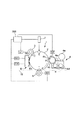
図1は、本実施例の画像形成装置100の概略構成図である。画像形成装置100は、イエロー、マゼンタ、シアン、ブラックの4色に対応して設けられ4つの画像形成ユニット1Y、1M、1C、1Bkを有する電子写真方式のフルカラープリンタである。本実施例にて、画像形成装置100は、画像形成装置本体に接続された原稿読み取り装置又は画像形成装置本体に対し通信可能に接続されたパーソナルコンピュータ等のホスト機器からの画像信号に応じて、4色フルカラー画像を記録材上に形成することができる。記録材としては、記録用紙、プラスチックフィルム、布等がある。
(Overall configuration and operation of image forming apparatus)
FIG. 1 is a schematic configuration diagram of an
各画像形成ユニット1Y、1M、1C、1Bkにて像担持体としての電子写真感光体2Y、2M、2C、2Bk上に形成されたトナー像を、転写媒体である中間転写体としての中間転写ベルト16上へ転写する。続いて、中間転写ベルト16上のトナー像を、記録材担持体としての搬送ベルト8により担持搬送される記録材P上に転写する構成となっている。
An intermediate transfer belt as an intermediate transfer member, which is a transfer medium, with toner images formed on the electrophotographic
尚、本実施例では、画像形成装置100が備える4つの画像形成ユニット1Y、1M、1C、1Bkは、現像色が異なることを除いて実質的に同一の構成を有する。従って、以下、特に区別を要しない場合は、いずれかの画像形成ユニットに属する要素であることを表すために符号に付した添え字Y、M、C、Bkは省略し、総括的に説明する。
In this embodiment, the four
画像形成ユニット1には、像担持体として円筒型の電子写真感光体、即ち、感光ドラム2が配設されている。感光ドラム2は、図中矢印方向に回転駆動される。
The
感光ドラム2の周囲には帯電手段としての帯電ローラ3と、現像手段としての現像装置4、転写手段としての一次転写ローラ5と、帯電補助手段としての帯電補助装置6が配置されている。
Around the
感光ドラム2の図中上方には、露光手段(潜像形成手段)としてのレーザースキャナ(露光装置)7が配置されている。又、各画像形成ユニット1の感光ドラム2と対向して中間転写ベルト16が配置されている。中間転写ベルト16は、駆動ローラ9、二次転写対向ローラ10、従動ローラ12に張設され、駆動ローラ9の駆動により図中矢印方向に周回移動し、トナー像を記録材Pとの当接部(二次転写位置)へと搬送する。中間転写ベルト16の下方には、記録材Pを担持し搬送する搬送ベルト8が配置される。搬送ベルト8は、二次転写対向ローラ10に対向配置された二次転写ローラ15と、支持ローラ17との間に張設され、図中矢印方向に周回移動される。中間転写ベルト16から記録材Pへトナー像を転写した後、続いて、定着装置13によってトナー像が記録材Pへ熱定着される。
A laser scanner (exposure device) 7 as an exposure means (latent image forming means) is disposed above the
次に、4色フルカラーの画像形成時について説明する。 Next, a description will be given of the case of four-color full-color image formation.
先ず、画像形成動作が開始すると、回転する感光ドラム2の表面が帯電ローラ3によって一様に帯電される。このとき、帯電ローラ3には、帯電バイアス電源S1より帯電バイアスが印加される。次いで、感光ドラム2は、露光装置7から発せられる画像信号に対応したレーザ光により露光される。これにより、感光ドラム2上に画像信号に応じた静電像(潜像)が形成される。感光ドラム2上の静電像は、現像装置4内に収容されたトナーによって顕像化され、可視像となる。本実施例では、レーザ光により露光した明部電位にトナーを付着させる反転現像方式を用いる。
First, when the image forming operation starts, the surface of the rotating
現像装置4により、感光ドラム2上にトナー像を形成し、中間転写ベルト16上にトナー像を一次転写する。一次転写後に感光ドラム2表面に残ったトナー(転写残トナー)は、補助帯電装置6を通過した後、再び現像装置4内へ回収される。
The developing
上記動作をイエロー、マゼンタ、シアン、ブラックで順次行い、中間転写ベルト16上で4色のトナー像を重ね合わせる。その後、トナー像の形成タイミングに合わせて記録材収納カセット(図示せず)に収容された記録材Pが供給ローラ14、搬送ベルト8により二次転写位置へと搬送される。そして、二次転写ローラ15に二次転写バイアスを印加することにより、中間転写ベルト16上の4色のトナー像を、搬送ベルト8上に担持されている記録材P上に一括で二次転写する。
The above operation is sequentially performed for yellow, magenta, cyan, and black, and the four color toner images are superimposed on the
次いで、記録材Pは搬送ベルト8から分離され、定着手段としての定着装置13に搬送される。この定着装置13によって、加熱、加圧されることで、記録材P上のトナーは溶融、混合されて、フルカラーの永久画像となる。その後、記録材Pは機外に排出される。 Next, the recording material P is separated from the conveyance belt 8 and conveyed to a fixing device 13 as a fixing unit. When the fixing device 13 is heated and pressurized, the toner on the recording material P is melted and mixed to form a full-color permanent image. Thereafter, the recording material P is discharged out of the apparatus.
又、二次転写ローラ15が配置された二次転写部で転写しきれずに中間転写ベルト16に残留したトナーは、中間転写ベルトクリーナー18により除去される。これにより、一連の動作が終了する。
The toner remaining on the
尚、所望の画像形成ユニットのみを用いて、所望の色の単色又は複数色の画像を形成することも可能である。 Note that it is also possible to form a single-color or multi-color image of a desired color using only a desired image forming unit.
(画像形成ユニットの動作)
次に、図2を参照して画像形成ユニット1における動作を詳細に説明する。
(Operation of image forming unit)
Next, the operation of the
本実施例において、感光ドラム2は、帯電特性が負帯電性の有機光導電体(OPC)であり、外径30mm、中心支軸を中心に矢示の反時計方向に回転駆動される。
In this embodiment, the
感光ドラム2表面を一様に帯電処理する帯電手段として、接触帯電装置(接触帯電器)3を有する。本実施例において、接触帯電装置3は、帯電ローラ(ローラ帯電器)であり、感光ドラム2との間の微小ギャップにて生じる放電現象を利用して帯電する。帯電ローラ3には、電源S1より所定の条件の帯電バイアス電圧が印加される。これにより、回転する感光ドラム2表面は、所定の極性、電位に接触帯電処理される。本実施例において、帯電ローラ3に対する帯電バイアス電圧は、直流電圧(Vdc)と交流電圧(Vac)とを重畳した振動電圧である。より具体的には、−500Vの直流電圧と、周波数1.3kHz、ピーク間電圧Vpp1.5kV、正弦波の交流電圧とを重畳した振動電圧である。この帯電バイアス電圧により、感光ドラム2表面は帯電ローラ3に印加した直流電圧と同じ−500V(暗電位Vd)に一様に接触帯電処理される。
A contact charging device (contact charger) 3 is provided as a charging means for uniformly charging the surface of the
本実施例においては、現像装置4は、トナーとキャリアを含む二成分現像剤による磁気ブラシを、感光ドラム2に接触させながら現像を行う二成分接触現像方式を採用した現像装置である。
In this embodiment, the developing
現像装置4は、現像容器4a、現像剤担持体としての非磁性の現像スリーブ4bを備えている。現像スリーブ4bは、その外周面の一部を現像装置4の外部に露呈させて、現像容器4a内に回転可能に配置してある。現像スリーブ4b内には、非回転に固定してマグネットローラ4cが挿設されている。現像容器4aは、二成分現像剤を収容しており、現像容器4a内の底部側には現像剤攪拌部材4dが配設されている。又、補給用トナーがトナーホッパー4eに収容されている。
The developing
現像容器4a内の二成分現像剤は、主に非磁性トナーと磁性キャリアとの混合物であり、現像剤攪拌部材4cにより攪拌される。本実施例において、トナーは、結着樹脂、着色剤、そして必要に応じてその他の添加剤を含む着色樹脂粒子を有している。トナーは、重合法により製造した負帯電性のポリエステル系樹脂であり、体積平均粒径は5μm以上8μm以下が好ましい。本実施例では6.2μmであった。トナーは磁性キャリアとの摺擦により負極性に摩擦帯電される。
The two-component developer in the developing
キャリアは、例えば、表面酸化或いは未酸化の鉄、ニッケル、コバルト、マンガン、クロム、希土類等の金属、及びそれらの合金、又は酸化物フェライトなどが好適に使用可能である。これらの磁性粒子の製造法は特に制限されない。そして、キャリアは、重量平均粒径が20〜50μm、好ましくは30〜40μmであり、抵抗率が107Ω・cm以上、好ましくは108Ω・cm以上である。本実施例では108Ω・cmのものを用いた。 As the carrier, for example, surface-oxidized or unoxidized iron, nickel, cobalt, manganese, chromium, rare earth and other metals, and alloys thereof, or oxide ferrite can be preferably used. The method for producing these magnetic particles is not particularly limited. The carrier has a weight average particle diameter of 20 to 50 μm, preferably 30 to 40 μm, and a resistivity of 10 7 Ω · cm or more, preferably 10 8 Ω · cm or more. In this example, 10 8 Ω · cm was used.
本実施例では、低比重磁性キャリアとして、フェノール系のバインダー樹脂に磁性金属酸化物及び非磁性金属酸化物と所定の比で混合し、重合法により製造した樹脂磁性キャリアを使用した。体積平均粒径は35μm、真密度は3.6〜3.7g/cm3、磁化量は53A・m2/kgである。 In this example, as the low specific gravity magnetic carrier, a resin magnetic carrier prepared by mixing a phenolic binder resin with a magnetic metal oxide and a nonmagnetic metal oxide at a predetermined ratio and using a polymerization method was used. The volume average particle diameter is 35 μm, the true density is 3.6 to 3.7 g / cm 3 , and the magnetization is 53 A · m 2 / kg.
現像スリーブ4bは、感光ドラム2との最近接距離(S−Dgap)を350μmに保持して感光ドラム2に近接対向配設される。この感光ドラム2と現像スリーブ4bとの対向部が現像部Aである。現像スリーブ4bは、現像部Aにおいて感光ドラム2の進行方向とは逆方向に回転駆動される。現像スリーブ4b内のマブネットローラ4cの磁力により、現像容器4a内の二成分現像剤の一部が現像スリーブ4bの外周面に磁気ブラシ層として吸着保持される。この磁気ブラシ層は、現像スリーブ4bの回転に伴い回転搬送され、現像部Aにおいて感光ドラム2の面に対して接触して感光ドラム面を適度に摺擦する。
The developing
現像スリーブ4bには、電源S2から所定の現像バイアスが印加される。本実施例において、現像スリーブ4bに対する現像バイアス電圧は、直流電圧(Vdc)と交流電圧(Vac)とを重畳した振動電圧である。より具体的には、−350Vの直流電圧と、周波数8.0kHz、ピーク間電圧1.8kV、矩形波の交流電圧とを重畳した振動電圧である。
A predetermined developing bias is applied from the power source S2 to the developing
そして、回転する現像スリーブ4bの面に薄層としてコーティングされ、現像部Aに搬送された現像剤中のトナーが、現像バイアスによる電界によって感光ドラム2の表面に静電潜像に対応して選択的に付着し、静電潜像がトナー像として現像される。現像部Aを通過した現像スリーブ4b上の現像剤薄層は、引き続く現像スリーブ4bの回転に伴い現像容器4a内の現像剤溜り部に戻される。
Then, the toner in the developer coated as a thin layer on the surface of the rotating developing
現像容器4a内の二成分現像剤のトナー濃度を、略一定の範囲内に維持するために、現像容器4a内の二成分現像剤のトナー濃度を、例えば、図示しない光学式トナー濃度センサによって検知する。そして、その検知情報に応じてトナーホッパー4e内に配置されている図示しないトナー補給スクリューの回転動作を制御するによって、現像容器4a内の二成分現像剤にトナーが補給される。二成分現像剤に補給されたトナーは、攪拌部材4dにより攪拌される。
In order to maintain the toner concentration of the two-component developer in the developing
本実施例において、転写手段として中間転写ベルト16を有する。本実施例においては、一次転写装置5は転写ローラである。一次転写ローラ5は、転写部Tにて感光ドラム2に所定の押圧力をもって圧接されている。一次転写ローラ5には電源S3からトナーの正規帯電極性である負極性とは逆極性である正極性の転写バイアス、本実施例では+2kVが印加される。これにより、中間転写ベルト16の表面に感光ドラム2の表面側のトナー像が順次に静電転写されていく。
In this embodiment, an
本実施例においては、クリーナーレスシステムを採用しており、中間転写ベルト16に対するトナー像転写後の感光ドラム2の表面に若干量残留する転写残トナー(残留トナー)を除去する専用のクリーニング装置を具備していない。
In this embodiment, a cleanerless system is employed, and a dedicated cleaning device for removing a transfer residual toner (residual toner) remaining on the surface of the
転写後の感光ドラム2面上の転写残トナーは、引き続く感光ドラム2の回転に伴い帯電部C、露光部Eを通って現像部Aに搬送されて、現像装置4により現像同時クリーニングにて除去・回収される(クリーナーレスシステム)。
The transfer residual toner on the surface of the
本実施例において、現像装置4の現像スリーブ4bは、上述のように現像部Aにおいて感光ドラム2の表面の進行方向とは逆方向に回転させている。このような現像スリーブ4bの回転は、感光ドラム2上の転写残トナーの回収に有利である。
In this embodiment, the developing
感光ドラム2上の転写残トナーは、露光部Eを通るので、露光工程はその転写残トナー上からなされる。通常は、転写残トナーの量は少ないため、転写残トナー上から露光工程を行うことによる大きな影響は現れない。但し、上述したように、転写残トナーには帯電極性が正規極性のもの、逆極性のもの(反転トナー)、帯電量が少ないものが混在している。その内の反転トナーや帯電量が少ないトナーが、帯電部Cを通過する際に帯電ローラ3に付着すると、帯電ローラ3が許容以上にトナーにより汚染してしまい帯電不良を生じることがある。
Since the transfer residual toner on the
又、感光ドラム2上の転写残トナーを、現像装置4により現像動作と同時に効果的に除去、回収するためには転写残トナーの帯電量が重要な因子となってくる。即ち、現像部Aに持ち運ばれる感光ドラム2上の転写残トナーは、その帯電極性が正規極性であり、且つ、その帯電量が現像装置4によって感光ドラム2の静電潜像を現像できるトナーの帯電量であることが好ましい。転写残トナーの帯電極性が反転している場合や帯電量が適切でない場合には、感光ドラム2上から現像装置4に除去、回収できず、不良画像の原因となる。
Further, in order to effectively remove and collect the transfer residual toner on the
そこで、本発明によると、転写手段(転写ローラ)5が設けられた転写部Tよりも感光ドラム2の回転方向下流側で、且つ、帯電手段(帯電ローラ)3が設けられた帯電部Cの上流側に帯電補助装置6が設けられている。
Therefore, according to the present invention, the charging unit C provided with the charging unit (charging roller) 3 and on the downstream side in the rotation direction of the
本実施例によると、帯電補助装置6は、第1の帯電補助手段として、感光ドラム2上の転写残トナーを均一化(即ち、除電)するための、残留トナー均一化手段(残留現像剤像均一化手段)6aを備えている。更に、本実施例では、第2の帯電補助手段(トナーに電荷を付与する電荷付与手段)としてのトナー帯電量制御手段(現像剤帯電量制御手段)6bが設けられている。トナー帯電量制御手段(現像剤帯電量制御手段)6bは、前記残留トナー均一化手段6aよりも感光ドラム2の回転方向下流側で、且つ、帯電部Cよりも感光ドラム2の回転方向上流側の位置に設けられている。このトナー帯電量制御手段6bは、転写残トナーの帯電極性を正規極性である負極性に揃える作用をなす。
According to this embodiment, the
一般的に、転写されずに感光ドラム2上に残留した転写残トナーは、反転トナーや帯電量が適切でないトナーが混在している。そこで、残留トナー均一化手段6aにより一度転写残トナーを除電し、次いでトナー帯電量制御手段6bで再度転写残トナーを正規極性に帯電処理する。これにより、帯電ローラ3への転写残トナーの付着防止を効果的に成すと共に、現像装置4での転写残トナーの除去、回収を完全に行うことができる。そのため、転写残トナー像パターンのゴースト像の発生も有効に防止される。
In general, the untransferred toner remaining on the
本実施例では、残留トナー均一化手段6a及びトナー帯電量制御手段6bは、適度の導電性を持ったブラシ状部材であり、ブラシ部を感光ドラム2の表面に接触させて配設されている。それぞれ残留トナー均一化手段6aと感光ドラム2の表面との接触部、トナー帯電量制御手段6bと感光ドラム2の表面との接触部を形成している。残留トナー均一化手段6aには、電源S4より正極性の直流電圧が印加されており、トナー帯電量制御手段6bには、電源S5より負極性の直流電圧が印加される。それぞれに印加される直流電圧の大きさは、装置内に設置した温湿度センサSにより検知した温度及び相対湿度より計算される絶対水分量により、図3(a)、(b)に示すごとく変化させている。例えば、温度23℃、絶対水分量10.5g/m3の環境下においては、残留トナー均一化手段6aには+250V、トナー帯電量制御手段6bには−750Vの直流電圧がそれぞれ印加される。
In the present embodiment, the residual toner uniformizing means 6a and the toner charge amount control means 6b are brush-like members having appropriate conductivity, and are arranged with the brush portion in contact with the surface of the
転写部Tにおいて、中間転写ベルト16へのトナー像の転写後に感光ドラム2上に残留する転写残トナーは、残留トナー均一化手段6aと感光ドラム2との接触部に至り、残留トナー均一化手段6aによりその電荷量が0μC/g近傍で均一化される。
In the transfer portion T, the transfer residual toner remaining on the
更に、残留トナー均一化手段6aで均一化された感光ドラム2の表面上の転写残トナーは、トナー帯電量制御手段6bと感光ドラム2との接触部に至り、トナー帯電量制御手段6bにより、その帯電極性が正規極性である負極性に揃えられる。転写残トナーの帯電極性を正規極性である負極性に揃えることにより、転写残トナーが帯電ローラ3へ付着するのを防止することができる。つまり、帯電ローラ3と感光ドラム2との接触部(帯電部C)で転写残トナーの上から感光ドラム2の表面上を帯電処理する際に、転写残トナーの感光ドラム2への鏡映力を大きくし、転写残トナーが帯電ローラ3へ付着するのを防止する。この為にトナー帯電量制御手段6bにより転写残トナーに与える帯電量は、現像時のトナー帯電量と比較すると約2倍以上であるのが好ましく、温度23℃、絶対水分量10.5g/m3の環境下では凡そ−50μC/gである。
Further, the transfer residual toner on the surface of the
第1及び第2帯電補助手段6a、6bにて構成される帯電補助装置6には、図示しないレシプロ機構が作動的に連結されていて、感光ドラム2の駆動とレシプロ機構の駆動が同一駆動となっている。このレシプロ機構によって各帯電補助手段6a、6bを主走査方向(感光ドラム2の回転軸線方向)に揺動させる。これによって、感光ドラム上の転写残トナーや、後に説明する研磨粒子を効率よくトナー帯電量制御手段6bに捕集することが出来る。
A reciprocating mechanism (not shown) is operatively connected to the charging
(転写残トナーの回収)
次に、現像工程における転写残トナーの回収について説明する。
(Recovery of transfer residual toner)
Next, recovery of transfer residual toner in the development process will be described.
現像装置4は、上述のように、現像と同時に転写残トナーを回収、清掃する。感光ドラム2上の静電潜像の現像に使用されるトナー帯電量(平均値)は、温度23℃、絶対水分量10.5g/m3の環境下においては凡そ−25μC/gである。感光ドラム2上の転写残トナーが現像装置4に十分に回収されるためには、現像装置4に到達する転写残トナーの帯電量が−15μC/g〜−35μC/gの範囲であることが好ましい。
As described above, the developing
しかし、上述のように、帯電ローラ3へのトナー付着を防止するためにトナー帯電量制御手段6bによって、−50μC/gと負極性に大きく帯電された転写残トナーは、現像装置4において回収させるためには除電を行う必要がある。
However, as described above, the transfer residual toner charged to a negative polarity of −50 μC / g by the toner charge amount control means 6b in order to prevent the toner from adhering to the charging roller 3 is collected in the developing
ここで、帯電ローラ3には感光ドラム2表面を帯電処理するために、交流電圧(周波数1.3kHz、ピーク間電圧Vpp=1.5kV)が印加されている。この時、帯電ローラ3が感光ドラム2表面を帯電処理すると同時に、感光ドラム2上の転写残トナーが交流除電される。斯かる交流電圧条件において、凡そ−50μC/gであった転写残トナーの帯電量は、帯電部Cの通過後におよそ−30μC/gとなる。これにより、現像工程において、感光ドラム2上のトナーが付着されるべきではない部分(非画像部)に付着した転写残トナーは、現像装置4に回収される。
Here, an AC voltage (frequency 1.3 kHz, peak-to-peak voltage Vpp = 1.5 kV) is applied to the charging roller 3 in order to charge the surface of the
かくして、
(i)感光ドラム2の回動に伴って転写部Tから帯電部Cへ搬送される転写残トナーの電荷量を、トナー帯電量制御手段6bで正規極性である負極性に揃えて帯電処理して転写残トナーの帯電ローラ3への付着を防止し、
(ii)帯電ローラ3で感光ドラム2を所定の電位に帯電すると同時に、トナー帯電量制御手段6bで正規極性である負極性に帯電処理された転写残トナーの帯電量を、現像装置4で感光ドラム2上の静電潜像を現像するのと同程度の帯電量に制御する。
Thus,
(I) The charge amount of the untransferred toner conveyed from the transfer portion T to the charging portion C as the
(Ii) The
これにより、現像装置4での転写残トナーの回収が効率的に行われる。
Thereby, the transfer residual toner is efficiently collected in the developing
上述のようなクリーナーレスシステム、特に現像同時クリーニング方式によれば、従来一般に用いられているようなクリーニング装置を特別に設ける必要がない。また、廃トナーを出さずに再利用することができ、メンテナンスの煩わしさ、装置の小型化に大きく貢献するばかりでなく、環境保全や資源の有効利用などの点で好ましい。 According to the cleaner-less system as described above, in particular, the simultaneous development cleaning method, there is no need to provide a cleaning device that is generally used conventionally. In addition, the toner can be reused without producing waste toner, which not only greatly contributes to the troublesome maintenance and downsizing of the apparatus, but is also preferable in terms of environmental conservation and effective use of resources.
また、本実施例においては、現像装置内の現像剤中、及び、補給トナー中に、トナーと逆極性に帯電する性質の研磨粒子を含有している。本実施例ではトナーが負帯電極性であり、研磨粒子は正帯電極性を示すチタン酸ストロンチウムを用いている。 In the present embodiment, the developer in the developing device and the replenishing toner contain abrasive particles having the property of being charged with a polarity opposite to that of the toner. In this embodiment, the toner has a negatively charged polarity, and strontium titanate having a positively charged polarity is used for the abrasive particles.
本実施例で用いているチタン酸ストロンチウムを具体的に説明すると、一次粒子の平均粒径が30nm以上300nm以下の範囲にあるもので、立方体状または直方体状の粒子形状をしていて、且つぺロブスカイト型結晶構造を成している。このようなチタン酸ストロンチウムを用いた場合、例えばクリーナーブレードのように感光ドラムを強力に摺擦する部材を有していない画像形成装置においても、放電生成物を効果的に除去することができる。本実施例では、研磨粒子の添加量はトナーに対して0.1〜6.0重量%、通常、0.2重量%としている。 The strontium titanate used in this example will be described in detail. The primary particles have an average particle size in the range of 30 nm to 300 nm, have a cubic or rectangular particle shape, and It has a lobskite crystal structure. When such strontium titanate is used, discharge products can be effectively removed even in an image forming apparatus that does not have a member that strongly rubs the photosensitive drum such as a cleaner blade. In this embodiment, the amount of abrasive particles added is 0.1 to 6.0% by weight, usually 0.2% by weight, based on the toner.
上述のように、研磨粒子をトナーと逆極性に帯電させることによって、中間転写ベルト16上に転写される研磨粒子量を極力減らし、安定して研磨粒子を帯電補助装置6に供給することができる。研磨粒子は、現像剤中に遊離していて、主に現像装置−感光ドラム間におけるかぶり取りバイアス(Vback電位)が発生したときに、現像スリーブ4bから感光ドラム2上に供給される。そして、研磨粒子は転写位置Tを通過後に帯電補助装置6に付着する。
As described above, by charging the abrasive particles with a polarity opposite to that of the toner, the amount of abrasive particles transferred onto the
本実施例においては、研磨粒子が正極性のものを用いているので、研磨粒子はトナー帯電量制御手段6bにより多く貯まる。本実施例では上記かぶり取りバイアス(Vback電位)は150Vである。 In the present embodiment, since abrasive particles having positive polarity are used, a large amount of abrasive particles is stored in the toner charge amount control means 6b. In this embodiment, the fog removal bias (Vback potential) is 150V.
図4に、通常画像形成時におけるタイミングチャートを示した。 FIG. 4 shows a timing chart during normal image formation.
本実施例において、単色画像形成時などにおいて画像形成を行うユニットと画像形成を行わないユニットが発生した場合においては、次のことが行われている。 In this embodiment, when a unit that performs image formation and a unit that does not perform image formation occur during the formation of a monochrome image, the following is performed.
つまり、画像形成を行わないユニットの感光ドラムを通常の画像形成時と同様に転写装置(中間転写体)に当接させた状態で、感光ドラムを空回転する。この方法を用いることによって転写装置の着脱機構などを設ける必要がないため、画像形成装置の小型化、低コスト化、更には高生産性を達成することができる。 That is, the photosensitive drum is idly rotated in a state where the photosensitive drum of a unit that does not perform image formation is in contact with the transfer device (intermediate transfer member) in the same manner as in normal image formation. By using this method, it is not necessary to provide an attaching / detaching mechanism for the transfer device, so that the image forming apparatus can be reduced in size, cost, and productivity can be achieved.
ここで、上記構成を採用している画像形成装置において発生した問題を説明する。 Here, a problem occurring in the image forming apparatus adopting the above configuration will be described.
本実施例において、ブラック単色画像形成を連続して行った場合、イエロー、マゼンタ、シアンの感光ドラムのみが空回転することによって、次の問題が発生した。 In this embodiment, when black monochromatic image formation was continuously performed, only the yellow, magenta, and cyan photosensitive drums were idled, causing the following problem.
つまり、帯電補助装置6に付着していた研磨粒子が回転する感光ドラムとの摺擦によって引き剥がれ、帯電補助装置6に付着している研磨粒子が枯渇してしまう。その結果、気温23℃、湿度70%の環境下で、ブラック単色画像形成を連続して1000枚行った場合、イエロー、マゼンタ、シアンの画像形成ユニットにおいて、帯電補助装置6に付着している研磨粒子が不足してしまった。そのため、その後の画像形成においてイエロー、マゼンタ、シアンにおいて画像流れが発生してしまった。
That is, the abrasive particles adhering to the
そこで、本実施例では、画像形成を行わない画像形成ユニットにおいては、感光ドラムと帯電補助手段との間に所定の電位差を形成することによって、帯電補助手段に付着する研磨粒子量が制御される。即ち、単色画像形成時に、画像形成を行わない他色の画像形成ユニットの帯電補助手段、即ち、トナー帯電量制御手段6bに研磨粒子と逆極性のバイアス(本実施例ではネガ極性のバイアス)を印加する。これによって、研磨粒子を保持するための電位差が形成され、ブラック単色画像形成を連続して行った場合においても他色のユニットの帯電補助手段6bに付着している研磨粒子が剥がれることを防止できる。そして、常に安定した量の研磨粒子を帯電補助手段6bに付着させることができた。 Therefore, in this embodiment, in an image forming unit that does not perform image formation, the amount of abrasive particles adhering to the charging auxiliary unit is controlled by forming a predetermined potential difference between the photosensitive drum and the charging auxiliary unit. . That is, when forming a single color image, a bias assisting means of an image forming unit of another color that does not form an image, that is, a toner charge amount control means 6b is biased with a polarity opposite to that of abrasive particles (in this embodiment, a negative polarity bias). Apply. As a result, a potential difference for holding the abrasive particles is formed, and even when black monochromatic image formation is continuously performed, it is possible to prevent the abrasive particles attached to the auxiliary charging means 6b of the other color units from being peeled off. . In addition, a stable amount of abrasive particles could always be adhered to the auxiliary charging means 6b.
以下に、図5、表1を用いて詳細を述べる。 Details will be described below with reference to FIG.
図5にブラック単色画像形成時におけるイエロー、マゼンタ、シアンのタイミングチャートを示した。画像形成装置がブラック単色画像形成を行う場合、画像形成を行わないイエロー、マゼンタ、シアンそれぞれのユニットの感光ドラムを空回転させる。このとき、感光ドラムが回転している間は帯電補助手段6のトナー帯電量制御手段6bに研磨粒子と逆極性(本実施例ではネガ極性)の直流電圧を印加することとした。 FIG. 5 shows a timing chart of yellow, magenta, and cyan when forming a black monochrome image. When the image forming apparatus performs black monochrome image formation, the photosensitive drums of the yellow, magenta, and cyan units that do not perform image formation are idled. At this time, while the photosensitive drum is rotating, a DC voltage having a polarity opposite to that of the abrasive particles (negative polarity in this embodiment) is applied to the toner charge amount control means 6b of the auxiliary charging means 6.
表1は、気温23℃、湿度70%の環境下において、ブラック単色連続1000枚出力後におけるトナー帯電量制御手段6bに印加する電圧と、そのときの研磨粒子の減少率を示した表である。プロセススピードは100mm/sec、150mm/sec、200mm/sec、250mm/secでそれぞれ行っている。 Table 1 is a table showing the voltage applied to the toner charge amount control means 6b after the output of 1,000 black single-color continuous sheets in an environment of an air temperature of 23 ° C. and a humidity of 70%, and the reduction rate of the abrasive particles at that time. . The process speed is 100 mm / sec, 150 mm / sec, 200 mm / sec, and 250 mm / sec, respectively.

表1より、プロセススピードがおよそ100〜250mm/secの範囲においては、トナー帯電量制御手段6bに−150Vの電圧を印加することによって以下の効果を得ることができる。即ち、ブラック単色画像形成を連続して1000枚行った場合においても、トナー帯電量制御手段6bに付着している研磨粒子量は殆ど変化せず、その後の画像形成においても画像流れは発生しなかった。 From Table 1, when the process speed is in the range of about 100 to 250 mm / sec, the following effects can be obtained by applying a voltage of −150 V to the toner charge amount control means 6 b. That is, even when 1000 black single-color image formations were performed continuously, the amount of abrasive particles adhering to the toner charge amount control means 6b hardly changed, and image flow did not occur in the subsequent image formation. It was.
尚、トナー帯電量制御手段6bに印加する電圧は、放電が開始する電圧以下にすることが望ましい。何故なら放電が発生してしまうと放電生成物が発生し感光ドラムに付着してしまうためである。 Note that the voltage applied to the toner charge amount control means 6b is preferably equal to or lower than the voltage at which discharge starts. This is because when a discharge occurs, a discharge product is generated and adheres to the photosensitive drum.
このように、本実施例によれば、単色画像形成時において、画像形成を行っていない他色のユニットの帯電補助手段、即ち、トナー帯電量制御手段6bに、研磨粒子と逆極性の電圧を印加する。これによって、帯電補助手段6bに付着する研磨粒子量が制御される。そのため、画像形成が行われず長期にわたって感光ドラムを空回転した場合においても、帯電補助装置6から研磨粒子が枯渇することを防止し、常に安定した量の研磨粒子を帯電補助装置6に付着させることができた。そして、その後の画像形成において画像流れが発生しない画像形成装置を提供することが出来た。
As described above, according to this embodiment, during the formation of a single color image, a voltage having a polarity opposite to that of the abrasive particles is applied to the charging auxiliary unit of the other color unit that is not performing image formation, that is, the toner charge
尚、本実施例においては、ブラック単色画像形成時に、画像形成を行わないイエロー、マゼンタ、シアンそれぞれの画像形成ユニットの感光ドラムが空回転している間は帯電補助手段6bに研磨粒子と逆極性の電圧を印加することとしている。しかし、これに限定されるものではなく、ブラック以外の単色で画像形成を行う場合、または複数色の画像形成ユニットで画像形成を行う場合においても、同様に構成することができる。つまり、この場合にも、画像形成を行わない画像形成ユニットにおいて感光ドラムが回転している間は帯電補助手段6bに研磨粒子と逆極性の電圧を印加することは有用である。
In this embodiment, when the black monochrome image is formed, while the photosensitive drums of the yellow, magenta, and cyan image forming units that do not perform image formation are idling, the charging
また、本実施例ではトナー帯電量制御手段6bに−150Vの電圧を印加しているがこれに限定されるものではない。上述のように、トナー帯電量制御手段6bと感光ドラム2の間の電位差が、放電が開始する電位差以下であれば本実施例と同様の効果が得られることは言うまでもない。
In this embodiment, a voltage of −150 V is applied to the toner charge amount control means 6b, but the present invention is not limited to this. As described above, it goes without saying that the same effect as in this embodiment can be obtained if the potential difference between the toner charge amount control means 6b and the
実施例2
次に、実施例2について説明する。
Example 2
Next, Example 2 will be described.
尚、本実施例における画像形成装置及び画像形成プロセスは、前述した実施例1とほぼ同一であるため、実施例1の記載を援用し、重複する説明は適宜省略する。 Note that the image forming apparatus and the image forming process in the present embodiment are substantially the same as those in the above-described first embodiment, and therefore, the description of the first embodiment is used and overlapping description is appropriately omitted.
実施例1においては、単色画像形成時などにおいて、画像形成を行っていない他色の画像形成ユニットの帯電補助手段、即ち、トナー帯電量制御手段6bに研磨粒子と逆極性のバイアスを印加する構成とした。この構成によって、画像形成が行われず長期にわたって感光ドラムを空回転した場合においても、帯電補助装置6から研磨粒子が枯渇することを防止し、常に安定した量の研磨粒子を帯電補助装置6に付着させることができた。
In the first exemplary embodiment, a bias having a polarity opposite to that of the abrasive particles is applied to the auxiliary charging means of the other color image forming unit in which image formation is not performed, that is, the toner charge amount control means 6b at the time of monochromatic image formation. It was. With this configuration, even when the photosensitive drum is idled for a long period of time without image formation, it is possible to prevent the abrasive particles from being depleted from the
本実施例では、画像形成装置の電源をオンしたときに行う感光ドラムの空回転動作を行うときに、帯電補助手段のトナー帯電量制御手段6bに研磨粒子と逆極性のバイアスを印加することとした。以下に詳細を述べる。 In this embodiment, a bias having a polarity opposite to that of the abrasive particles is applied to the toner charge amount control means 6b of the auxiliary charging means when the photosensitive drum is idly rotated when the power of the image forming apparatus is turned on. did. Details are described below.
画像形成装置の長期放置後で発生する画像流れを防止するために、画像形成装置の電源をオンしたときに感光ドラムの空回転動作を所定の時間行うことによって、感光ドラム表面に付着している放電生成物を除去することが一般的に広く行われている。本実施例における画像形成装置においても感光ドラムの空回転動作を行っている(本実施例では100秒間)。従って、本実施例では帯電補助装置6に研磨粒子を堆積させることによって、感光ドラムの空回転中に効果的に放電生成物を除去することが出来る。
In order to prevent the image flow that occurs after the image forming apparatus is left for a long time, the photosensitive drum is adhered to the surface of the photosensitive drum by performing the idling operation of the photosensitive drum for a predetermined time when the power of the image forming apparatus is turned on. It is generally widely practiced to remove discharge products. Also in the image forming apparatus in this embodiment, the photosensitive drum is idly rotated (100 seconds in this embodiment). Therefore, in this embodiment, by depositing abrasive particles on the
しかし、画像形成装置の電源をオンする毎に感光ドラムの空回転動作が繰り返し行われるため、回転する感光ドラムとの摺擦によって帯電補助装置6から研磨粒子が徐々に剥がれてしまう。そのために、帯電補助装置6に付着している研磨粒子が枯渇してしまうという問題が発生した。
However, each time the power of the image forming apparatus is turned on, the idle rotation of the photosensitive drum is repeatedly performed. Therefore, the abrasive particles are gradually peeled off from the
そこで本実施例では、画像形成装置の電源をオンしたときに行う感光ドラムの空回転動作を行うときに、帯電補助装置6のトナー帯電量制御手段6bに研磨粒子と逆極性のバイアスを印加することとした。
In this embodiment, therefore, a bias having a polarity opposite to that of the abrasive particles is applied to the toner charge amount control means 6b of the
図6に、電源をオン後に行う感光ドラムの空回転動作を行うときのタイミングチャートを示した。 FIG. 6 shows a timing chart when the idling operation of the photosensitive drum performed after the power is turned on.
尚、本発明では上記の感光ドラム空回転動作を行うとき(空回転動作中)は、帯電ローラ3に電圧を印加していない。これは非画像形成中などに帯電電圧を余計に印加することによる、感光ドラム2の放電劣化を防止するためである。
In the present invention, no voltage is applied to the charging roller 3 when the above-mentioned photosensitive drum idling operation is performed (during idling operation). This is to prevent discharge deterioration of the
本実施例では画像形成装置の電源オン時に、帯電補助装置6のトナー帯電量制御手段6bに−150Vの電圧を印加した状態で、感光ドラム2の空回転を行なうモードを実行する。本実施例では上記モードを実行する実行手段(制御手段)としてのCPU300により100秒間行うこととしている。CPU300は、図2のように、各電源S1〜S5を制御し、ドラムを回転させることで上記モードを実行する。これによって感光ドラム表面に堆積した放電生成物を除去することができ、高湿環境下においても画像流れの発生を抑制することが出来た。更に、感光ドラム2の空回転が繰り返し行われた場合においても、帯電補助手段6bに付着している研磨粒子が剥がれることを防止し、常に画像流れの発生しない安定した画像形成を行うことが出来た。
In this embodiment, when the power of the image forming apparatus is turned on, a mode in which the
尚、本実施例においては、画像形成装置の電源をオンしたときに行う感光ドラムの空回転動作を行うときに帯電補助手段6bに研磨粒子と逆極性のバイアスを印加することとしたが、これに限定されるものではない。例えば、電源をオンした後の、コピージョブ開始時の前回転時、またはコピージョブ終了後の後回転時、更にはコピージョブ中に感光ドラムが空回転するときに帯電補助手段6bに研磨粒子と逆極性のバイアスを印加しても有用である。
In this embodiment, a bias having a polarity opposite to that of the abrasive particles is applied to the auxiliary charging means 6b when the photosensitive drum is idled when the power of the image forming apparatus is turned on. It is not limited to. For example, after turning on the power, when the pre-rotation at the start of the copy job, at the post-rotation after the end of the copy job, or when the photosensitive drum is idly rotated during the copy job, the charging
実施例3
次に、実施例3について説明する。
Example 3
Next, Example 3 will be described.
尚、本実施例における画像形成装置及び画像形成プロセスは、前述した実施例1、2とほぼ同一であるため、実施例1、2の記載を援用し、重複する説明は適宜省略する。 The image forming apparatus and the image forming process in the present embodiment are almost the same as those in the first and second embodiments. Therefore, the description of the first and second embodiments is used, and a duplicate description is omitted as appropriate.
実施例1、2においては、非画像形成中に感光ドラム2が空回転動作を行う場合、感光ドラム2と帯電補助手段6bとの間に所望の電位差を形成することによって、感光ドラムが空回転動作を行うことによって研磨粒子が剥がれることを防止することとした。
In the first and second embodiments, when the
しかし、例えばブラック単色画像形成を長期間行うユーザーなどにおいては、イエロー、マゼンタ、シアンユニットの感光ドラムの空回転動作が長期にわたって行われ、且つイエロー、マゼンタ、シアンユニットでの画像形成が行われない。そのため帯電補助装置6に研磨粒子の供給が行われない。その結果、実施例1、2のような手段を採用した場合においても、帯電補助装置6の研磨粒子が枯渇してしまい、画像流れが発生してしまうことがまれにあった。
However, for example, for a user who performs black monochrome image formation for a long period of time, the photosensitive drums of yellow, magenta, and cyan units are idled for a long period of time, and image formation is not performed with yellow, magenta, and cyan units. . Therefore, the abrasive particles are not supplied to the
そこで本実施例においては、以下のような動作を行なっている。即ち、単色画像形成中の所定タイミングにおいて、非画像形成ユニットの感光ドラム2と帯電補助手段6bの間に所望の電位差を形成させ、且つ非画像形成ユニットの現像装置4から帯電補助装置6への研磨粒子の供給動作を行うこととした。以下に詳細を述べる。
Therefore, in this embodiment, the following operation is performed. That is, at a predetermined timing during monochromatic image formation, a desired potential difference is formed between the
画像形成装置がブラック単色画像形成を行う場合、画像形成を行わないイエロー、マゼンタ、シアンそれぞれの画像形成ユニットの感光ドラム2を空回転させる。このとき、感光ドラム2が回転している間は帯電補助装置6のトナー帯電量制御手段6bに−150Vの電圧を印加することとした。
When the image forming apparatus performs black monochrome image formation, the
図7に示したフローチャートに従って説明する。設定されたタイミングにて、本実施例ではブラック単色画像形成の印字枚数が連続してある所定の枚数(本実施例では3000枚)に達した場合、画像形成を行わない画像形成ユニットの帯電ローラ3及び現像スリーブ4bに所定の電圧を印加する。これによって感光ドラム2と現像スリーブ4bとの間に電位差を形成する。本実施例では帯電ローラ3に−400V、現像スリーブ4bに−200Vの電圧をそれぞれ印加している。そして、現像装置4の駆動を30秒間オンにすることによって、感光ドラム−現像スリーブ間の電位差を利用して研磨粒子を現像装置4から吐き出す。吐き出された研磨粒子は帯電補助装置6に捕集される。
This will be described with reference to the flowchart shown in FIG. In this embodiment, when the number of black monochrome image formations reaches a predetermined number (3000 in this embodiment) at the set timing, the charging roller of the image forming unit that does not perform image formation. 3 and a predetermined voltage are applied to the developing
図8に、ブラック単色画像形成時におけるイエロー、マゼンタ、シアンのタイミングチャートを示した。本実施例において上記の研磨粒子の供給動作をブラック画像形成中に行っているが、ブラック画像形成終了後の後回転時に行ってもよい。 FIG. 8 shows a timing chart of yellow, magenta, and cyan when forming a black monochrome image. In the present embodiment, the above-described abrasive particle supply operation is performed during black image formation, but may be performed during post-rotation after completion of black image formation.
このように、単色画像形成中において、非画像形成ユニットの感光ドラム2とトナー帯電量制御手段6bの間に所望の電位差を形成し、ある所定のタイミングで非画像形成ユニットの現像装置4から帯電補助手段6bへの研磨粒子の供給動作を行う。この構成によって、画像形成が行われず長期にわたって感光ドラム2を空回転した場合においても、帯電補助装置6から研磨粒子が枯渇することを防止し、常に安定した量の研磨粒子を帯電補助装置6に付着させることができる。それによって、画像流れが発生しない画像形成装置を提供することが出来た。
In this way, during monochromatic image formation, a desired potential difference is formed between the
尚、本実施例においては、ブラック単色画像形成時に画像形成を行わないイエロー、マゼンタ、シアンそれぞれの画像形成ユニットの感光ドラムが空回転している間は、帯電補助手段6bに研磨粒子と逆極性の電圧を印加する。且つ、ある所定のタイミングで非画像形成ユニットの現像装置4から帯電補助手段6bへの研磨粒子の供給動作を行うこととしている。
In this embodiment, when the photosensitive drum of each of the yellow, magenta, and cyan image forming units that do not perform image formation during black monochrome image formation is idling, the charging
しかし、これに限定されるものではなく、ブラック以外の単色で画像形成を行う場合、または複数色の画像形成ユニットで画像形成を行う場合においても、同様に行うことができる。つまり、画像形成を行わない画像形成ユニットにおいて感光ドラムが回転している間は帯電補助手段6bに研磨粒子と逆極性の電圧を印加し、且つ所定タイミングで非画像形成ユニットの現像装置4から帯電補助装置6への研磨粒子の供給動作を行っても有用である。
However, the present invention is not limited to this, and the same can be done when image formation is performed with a single color other than black, or when image formation is performed with a plurality of color image formation units. That is, while the photosensitive drum is rotating in an image forming unit that does not perform image formation, a voltage having a polarity opposite to that of the abrasive particles is applied to the charging
実施例4
次に、実施例4について説明する。
Example 4
Next, Example 4 will be described.
尚、本実施例における画像形成装置及び画像形成プロセスは、前述した実施例1、2、3とほぼ同一であるため、実施例1、2、3の記載を援用し、重複する説明は適宜省略する。 Note that the image forming apparatus and the image forming process in the present embodiment are almost the same as those in the first, second, and third embodiments described above. To do.
実施例3においては、単色画像形成中において、非画像形成ユニットの感光ドラム2と帯電補助手段6bの間に所望の電位差を形成し、且つ、ある所定のタイミングで非画像形成ユニットの現像装置4から帯電補助手段6bへの研磨粒子の供給動作を行うこととした。
In the third embodiment, during monochromatic image formation, a desired potential difference is formed between the
図9に、電源をオン後に行う感光ドラムの空回転動作を行うときのタイミングチャートを示した。 FIG. 9 shows a timing chart when the idling operation of the photosensitive drum is performed after the power is turned on.
本実施例では、実施例2と同様に画像形成装置の電源オン時に帯電補助装置6のトナー帯電量制御手段6bに、−150Vの電圧を印加した状態で感光ドラム2の空回転を100秒間行うこととした。更に、感光ドラム2の空回転開始とほぼ同時に、現像装置4の現像スリーブ4bに+200の電圧を印加することとした。そして現像装置4の駆動を10秒間オンにすることによって、感光ドラム−現像スリーブ間の電位差を利用して研磨粒子を現像装置から吐き出す。そして吐き出された研磨粒子は帯電補助装置6に捕集される。
In this embodiment, as in the second embodiment, when the image forming apparatus is turned on, the
これによって画像形成が行われず長期にわたって感光ドラムを空回転した場合においても、帯電補助装置6から研磨粒子が枯渇することを防止し、常に安定した量の研磨粒子を帯電補助装置6、即ち、トナー帯電量制御手段6bに付着させることができた。それによって、画像流れが発生しない画像形成装置を提供することが出来た。
Thus, even when the photosensitive drum is idled for a long period of time without image formation, it is possible to prevent the abrasive particles from being depleted from the
上記各実施例では、本発明は、中間転写方式の画像形成装置に適用されるものであるとして説明したが、本発明の画像形成装置は、これに限定されるものではない。 In the above embodiments, the present invention has been described as being applied to an intermediate transfer type image forming apparatus, but the image forming apparatus of the present invention is not limited to this.
つまり、本発明は、例えば、図10に概略図示するように、感光ドラム2上のトナー像を転写装置5にて直接、転写媒体、即ち、記録材Pに転写する方式の画像形成装置にも同様に適用することができる。図10の画像形成装置は、中間転写体としての中間転写ベルト16の代わりに、記録材Pを搬送する搬送ベルト8を備えている。この実施例では、中間転写ベルトを備えていない点を除けば、図1、図2に関連して説明した先の実施例の画像形成装置及び画像形成ユニットと同様の構成とされる。従って、同じ構成及び機能を成す部材には同じ参照番号を付し、先の実施例の説明を援用する。図10に示す画像形成装置も、先の実施例の画像形成装置と同様の作用効果を奏し得る。
That is, the present invention is also applied to an image forming apparatus that transfers a toner image on the
1 画像形成ユニット
3 帯電ローラ(帯電手段)
2 感光ドラム(像担持体)
4 現像装置(現像手段)
4b 現像スリーブ(現像剤担持体)
4c マグネットローラ(磁界発生手段)
5 一次転写ローラ(転写手段)
6 帯電補助装置
6a 残留現像剤(トナー)均一化手段(第1の帯電補助手段)
6b 現像剤(トナー)帯電量制御手段(第2の帯電補助手段:電荷付与手段)
8 搬送ベルト(記録材担持体)
16 中間転写ベルト(中間転写体、転写媒体)
P 記録材(転写媒体)
1 Image forming unit 3 Charging roller (charging means)
2 Photosensitive drum (image carrier)
4 Developing device (Developing means)
4b Development sleeve (developer carrier)
4c Magnet roller (magnetic field generating means)
5 Primary transfer roller (transfer means)
6 Charging
6b Developer (toner) charge amount control means (second charge auxiliary means: charge application means)
8 Conveyor belt (recording material carrier)
16 Intermediate transfer belt (intermediate transfer member, transfer medium)
P Recording material (transfer medium)
Claims (7)
トナー像を担持する像担持体と、
前記像担持体の表面を帯電する帯電手段と、
前記帯電手段により帯電された前記像担持体上に静電潜像を形成する潜像形成手段と、
トナーと、前記トナーと帯電極性が逆極性で前記像担持体を研磨する研磨粒子と、を含む現像剤にて該静電潜像を現像する現像手段と、
前記像担持体上に形成されたトナー像を記録材上に転写する転写手段と、
前記現像手段から供給される研磨粒子を表面に担持するとともに、前記研磨粒子を前記転写手段にて転写されずに前記像担持体上に残ったトナーに接触させて電荷を付与する電荷付与手段と、
前記複数の画像形成ユニットの各像担持体とそれぞれ接触して配置され、各像担持体からのトナー像が転写される中間転写体、もしくは前記複数の画像形成ユニットの各像担持体とそれぞれ接触して配置され、記録材を前記各像担持体の転写位置に担持搬送する記録材担持体と、を有する画像形成装置において、
前記複数の画像形成ユニットのうち、一部の画像形成ユニットを用いて画像形成を行う場合、画像形成を行わないユニットの像担持体を前記中間転写体もしくは前記記録材担持体とともに回転させるとともに、前記電荷付与手段に前記研磨粒子と逆極性の電圧を印加することを特徴とする画像形成装置。 The image forming unit includes a plurality of image forming units,
An image carrier for carrying a toner image;
Charging means for charging the surface of the image carrier;
A latent image forming unit that forms an electrostatic latent image on the image carrier charged by the charging unit;
Developing means for developing the electrostatic latent image with a developer containing toner and abrasive particles for polishing the image carrier with the toner and the charging polarity opposite to each other;
Transfer means for transferring a toner image formed on the image carrier onto a recording material;
A charge applying unit that holds the abrasive particles supplied from the developing unit on the surface and applies the charge by bringing the abrasive particles into contact with the toner remaining on the image carrier without being transferred by the transfer unit; ,
An intermediate transfer member that is disposed in contact with each image carrier of each of the plurality of image forming units and to which a toner image from each image carrier is transferred, or each image carrier of each of the plurality of image forming units. And a recording material carrier that carries and transports the recording material to the transfer position of each image carrier,
When performing image formation using a part of the plurality of image forming units, the image carrier of the unit that does not perform image formation is rotated together with the intermediate transfer member or the recording material carrier, An image forming apparatus, wherein a voltage having a polarity opposite to that of the abrasive particles is applied to the charge applying unit.
前記像担持体の表面を帯電する帯電手段と、
前記帯電手段により帯電された前記像担持体上に静電潜像を形成する潜像形成手段と、
トナーと、前記トナーと帯電極性が逆極性で前記像担持体を研磨する研磨粒子と、を含む現像剤にて該静電潜像を現像する現像手段と、
前記像担持体上に形成されたトナー像を記録材上に転写する転写手段と、
前記現像手段から供給される研磨粒子を表面に担持するとともに、前記研磨粒子を前記転写手段にて転写されずに前記像担持体上に残ったトナーに接触させて電荷を付与する電荷付与手段と、を有する画像形成装置において、
非画像形成中において、前記現像手段から前記電荷付与手段へ研磨粒子の供給動作を行うとともに、前記電荷付与手段に前記研磨粒子と逆極性の電圧を印加させて前記像担持体を空回転させるモードを実行する実行手段を有することを特徴とする画像形成装置。 An image carrier for carrying a toner image;
Charging means for charging the surface of the image carrier;
A latent image forming unit that forms an electrostatic latent image on the image carrier charged by the charging unit;
Developing means for developing the electrostatic latent image with a developer containing toner and abrasive particles for polishing the image carrier with the toner and the charging polarity opposite to each other;
Transfer means for transferring a toner image formed on the image carrier onto a recording material;
A charge applying unit that holds the abrasive particles supplied from the developing unit on the surface and applies the charge by bringing the abrasive particles into contact with the toner remaining on the image carrier without being transferred by the transfer unit; In an image forming apparatus having
During non-image formation, a mode in which abrasive particles are supplied from the developing unit to the charge applying unit and a voltage having a polarity opposite to that of the abrasive particles is applied to the charge applying unit to idle the image carrier. An image forming apparatus having execution means for executing the above.
Priority Applications (2)
| Application Number | Priority Date | Filing Date | Title |
|---|---|---|---|
| JP2006322677A JP4939187B2 (en) | 2006-11-29 | 2006-11-29 | Image forming apparatus |
| US11/944,899 US8027617B2 (en) | 2006-11-29 | 2007-11-26 | Image forming apparatus |
Applications Claiming Priority (1)
| Application Number | Priority Date | Filing Date | Title |
|---|---|---|---|
| JP2006322677A JP4939187B2 (en) | 2006-11-29 | 2006-11-29 | Image forming apparatus |
Publications (3)
| Publication Number | Publication Date |
|---|---|
| JP2008139355A JP2008139355A (en) | 2008-06-19 |
| JP2008139355A5 JP2008139355A5 (en) | 2010-01-14 |
| JP4939187B2 true JP4939187B2 (en) | 2012-05-23 |
Family
ID=39463855
Family Applications (1)
| Application Number | Title | Priority Date | Filing Date |
|---|---|---|---|
| JP2006322677A Expired - Fee Related JP4939187B2 (en) | 2006-11-29 | 2006-11-29 | Image forming apparatus |
Country Status (2)
| Country | Link |
|---|---|
| US (1) | US8027617B2 (en) |
| JP (1) | JP4939187B2 (en) |
Families Citing this family (5)
| Publication number | Priority date | Publication date | Assignee | Title |
|---|---|---|---|---|
| JP5230461B2 (en) * | 2009-01-23 | 2013-07-10 | キヤノン株式会社 | Image forming apparatus |
| JP5623180B2 (en) * | 2010-08-20 | 2014-11-12 | キヤノン株式会社 | Image forming apparatus |
| JP5839841B2 (en) * | 2011-05-26 | 2016-01-06 | キヤノン株式会社 | Image forming apparatus |
| JP6635008B2 (en) * | 2016-12-02 | 2020-01-22 | 京セラドキュメントソリューションズ株式会社 | Image forming device |
| JP7016649B2 (en) * | 2017-09-08 | 2022-02-07 | キヤノン株式会社 | Image forming device |
Family Cites Families (15)
| Publication number | Priority date | Publication date | Assignee | Title |
|---|---|---|---|---|
| JP3278800B2 (en) * | 1997-08-29 | 2002-04-30 | キヤノン株式会社 | Image forming device |
| JP2000047545A (en) | 1998-07-27 | 2000-02-18 | Canon Inc | Image forming device |
| JP3337994B2 (en) * | 1999-01-26 | 2002-10-28 | キヤノン株式会社 | Image forming device |
| JP3728166B2 (en) * | 1999-02-12 | 2005-12-21 | キヤノン株式会社 | Image forming apparatus |
| US6421512B2 (en) | 1999-12-28 | 2002-07-16 | Canon Kabushiki Kaisha | Image forming apparatus with image bearing member charger that reduces the amount of toner electric charge |
| JP3647345B2 (en) * | 2000-01-31 | 2005-05-11 | キヤノン株式会社 | Image forming apparatus |
| JP4343376B2 (en) | 2000-01-31 | 2009-10-14 | キヤノン株式会社 | Image forming apparatus and process cartridge |
| JP4065496B2 (en) * | 2002-04-19 | 2008-03-26 | キヤノン株式会社 | Image forming apparatus |
| JP2004117960A (en) * | 2002-09-27 | 2004-04-15 | Canon Inc | Image forming apparatus |
| JP2004126246A (en) * | 2002-10-02 | 2004-04-22 | Canon Inc | Image forming apparatus |
| JP3758653B2 (en) * | 2003-08-13 | 2006-03-22 | 村田機械株式会社 | Photoconductor polishing apparatus and image forming apparatus having the same |
| JP2005300751A (en) * | 2004-04-08 | 2005-10-27 | Canon Inc | Image forming apparatus |
| EP1628172B1 (en) * | 2004-05-14 | 2017-09-20 | Canon Kabushiki Kaisha | Image forming method |
| JP2006235524A (en) * | 2005-02-28 | 2006-09-07 | Canon Inc | Image forming method |
| JP4865408B2 (en) | 2006-06-09 | 2012-02-01 | キヤノン株式会社 | Image forming apparatus |
-
2006
- 2006-11-29 JP JP2006322677A patent/JP4939187B2/en not_active Expired - Fee Related
-
2007
- 2007-11-26 US US11/944,899 patent/US8027617B2/en not_active Expired - Fee Related
Also Published As
| Publication number | Publication date |
|---|---|
| US8027617B2 (en) | 2011-09-27 |
| US20080124124A1 (en) | 2008-05-29 |
| JP2008139355A (en) | 2008-06-19 |
Similar Documents
| Publication | Publication Date | Title |
|---|---|---|
| JP5094445B2 (en) | Image forming apparatus | |
| JP5053602B2 (en) | Image forming apparatus | |
| JP4872026B2 (en) | Image forming apparatus | |
| JP4865408B2 (en) | Image forming apparatus | |
| JP4939187B2 (en) | Image forming apparatus | |
| JP2008129066A (en) | Image forming apparatus | |
| JP5142505B2 (en) | Image forming apparatus | |
| JP2004061661A (en) | Image forming apparatus | |
| JP5121216B2 (en) | Image forming apparatus | |
| JP2008122720A (en) | Image forming apparatus | |
| JP4058591B2 (en) | Image forming apparatus | |
| JP2003076215A (en) | Image forming apparatus | |
| JP4332336B2 (en) | Image forming apparatus | |
| JP4847259B2 (en) | Image forming apparatus | |
| JP2009116096A (en) | Image forming apparatus | |
| JP2007065591A (en) | Image forming apparatus | |
| JP2008009149A (en) | Image forming apparatus | |
| JP2007322634A (en) | Image forming apparatus | |
| JP2001042602A (en) | Image forming device and replenishing container for developer and magnetic particles for electrifying | |
| JP2010066416A (en) | Image forming apparatus | |
| JP4439669B2 (en) | Image forming apparatus | |
| JP4617134B2 (en) | Image forming apparatus | |
| JP4673034B2 (en) | Image forming apparatus | |
| JP2017090827A (en) | Image forming apparatus | |
| JP2008015148A (en) | Image forming apparatus |
Legal Events
| Date | Code | Title | Description |
|---|---|---|---|
| A521 | Request for written amendment filed |
Free format text: JAPANESE INTERMEDIATE CODE: A523 Effective date: 20091119 |
|
| A621 | Written request for application examination |
Free format text: JAPANESE INTERMEDIATE CODE: A621 Effective date: 20091119 |
|
| TRDD | Decision of grant or rejection written | ||
| A01 | Written decision to grant a patent or to grant a registration (utility model) |
Free format text: JAPANESE INTERMEDIATE CODE: A01 Effective date: 20120221 |
|
| A01 | Written decision to grant a patent or to grant a registration (utility model) |
Free format text: JAPANESE INTERMEDIATE CODE: A01 |
|
| A61 | First payment of annual fees (during grant procedure) |
Free format text: JAPANESE INTERMEDIATE CODE: A61 Effective date: 20120224 |
|
| FPAY | Renewal fee payment (event date is renewal date of database) |
Free format text: PAYMENT UNTIL: 20150302 Year of fee payment: 3 |
|
| R151 | Written notification of patent or utility model registration |
Ref document number: 4939187 Country of ref document: JP Free format text: JAPANESE INTERMEDIATE CODE: R151 |
|
| FPAY | Renewal fee payment (event date is renewal date of database) |
Free format text: PAYMENT UNTIL: 20150302 Year of fee payment: 3 |
|
| LAPS | Cancellation because of no payment of annual fees |