【0001】
【発明の属する技術分野】
本発明は、電子写真方式・静電記録方式等を用いた画像形成装置に関し、特に、複写機、プリンタ、ファクシミリなどの画像形成装置に関する。
【0002】
【従来の技術】
従来、電子写真方式を用いた複写機、プリンタ、ファクシミリなどの画像形成装置は、一般に、回転ドラム型の像担持体である電子写真感光体(感光体)、その感光体を所定の極性・電位に一様に帯電処理する帯電装置(帯電工程)、帯電処理された感光体に静電潜像を形成する情報書き込み手段としての露光装置(露光工程)、感光体上に形成された静電潜像を現像剤としてのトナーにより現像剤像(トナー画像)として顕像化する現像装置(現像工程)、トナー画像を感光体の表面から紙などの記録材に転写する転写装置(転写工程)、転写工程後の感光体上に多少ながら残余するトナー(残留現像剤、転写残トナー)を除去して感光体面を清掃するクリーニング装置(クリーニング工程)、記録材上のトナー画像を定着させる定着装置(定着工程)などを備えており、感光体には繰り返して電子写真プロセス(帯電工程・露光工程・現像工程・転写工程・クリーニングエ程)が適用されて作像に供される。
【0003】
転写工程後の感光体上に残余するトナーはクリーニング装置により感光体の表面から除去され、クリーニング装置内に回収されて廃トナーとなる。しかし、環境保全や資源の有効利用などの点から、このような廃トナーが出ないことが望ましい。
【0004】
そこで、クリーニング装置にて回収されている転写残トナー、所謂、廃トナーを現像装置に戻して再利用する画像形成装置が提案されている。
【0005】
また、クリーニング装置を廃し、転写工程後の感光体上の転写残トナーを現像装置において「現像同時クリーニング」で感光体上から除去・回収し、再利用するようにしたクリーナレス方式の画像形成装置が提案されている。
【0006】
現像同時クリーニングは、転写工程後の感光体上の転写残トナーを、次工程以降の現像工程時に現像装置に回収する。即ち、転写残トナーが付着した感光体を引き続き帯電、露光して静電潜像を形成し、この静電潜像の現像工程時にかぶり取りバイアス(現像装置に印加する直流電圧と感光体の表面電位間の電位差であるかぶり取り電位差Vback)によって、感光体表面に残余した転写残トナーのうち、現像されるべきでない部分(非画像部)上に存在する転写残トナーを現像装置に除去・回収する方法である。
【0007】
この方式によれば、転写残トナーは現像装置に回収されて次工程以降の静電潜像の現像に再利用されるため、廃トナーをなくし、又メンテナンス時に手を煩わせることも少なくすることができる。又、クリーナレスであるこトナー画像形成装置の小型化にも有利である。
【0008】
上述のような現像同時クリーニングを採用したクリーナレス方式の画像形成装置において、帯電装置として感光体に当接して感光体表面を帯電処理する接触帯電装置を用いる場合、感光体上の転写残トナーが感光体と接触帯電装置との接触ニップ部(帯電部)を通過する際に、転写残トナー中の、特に、帯電極性が正規極性とは逆極性に反転しているトナーが接触帯電装置に付着することがある。これにより、接触帯電装置が許容以上にトナー汚染され、帯電不良の原因となる虞がある。
【0009】
即ち、現像剤としてのトナーには、量的には少ないながら、帯電極性がもともと正規極性とは逆極性に反転しているトナーが混在している。又、帯電極性が正規極性のトナーであっても、転写バイアスや剥離放電などに影響されて帯電極性が反転するものや、除電されて帯電量が少なくなるものもある。
【0010】
そのため、転写残トナーには帯電極性が正規極性のもの、逆極性の反転トナー、帯電量が少ないものが混在しており、そのうちの反転トナーや帯電量が少ないトナーが感光体と接触帯電装置との接触ニップ部(帯電部)を通過する際に接触帯電装置に付着してしまう。
【0011】
また、感光体上の転写残トナーを現像同時クリーニングにて除去・回収するためには、帯電部を通過して現像部に持ち運ばれる感光体上の転写残トナーの帯電極性が正規極性であり、且つ、その帯電量が現像装置によって感光体の静電潜像を現像できるトナーの帯電量であることか必要である。反転トナーや帯電量が適切でないトナーについては、感光体上から現像装置に除去・回収できず、不良画像の原因となってしまう虞がある。
【0012】
接触帯電装置へのトナーの付着を防出するために、転写部から帯電部へ持ち運ばれる帯電極性が正規極性のもの、逆極性のもの、帯電量が少ないものが混在している感光体上の転写残トナーを、正規極性へと帯電付与して帯電極性を正規極性に揃えると共に、その帯電量を均一化する必要がある。
【0013】
そこで、従来、帯電補助手段として、感光体の移動方向において接触帯電装置より上流、且つ、転写手段より下流に位置していて、転写残トナーを帯電するトナー帯電量制御手段と、このトナー帯電量制御手段より上流、且つ、転写手段より下流に位置していて、感光体上の転写残トナーを均一化する転写残トナー均一化手段(残留トナー均一化手段)と、を感光体表面に当接させて設け、これら残留トナー均一化手段、トナー帯電量制御手段に一定の直流電圧を印加することによりこの問題を解決している(例えば、特許文献1、2参照)。
【0014】
つまり、転写後に感光体上に残留する残留トナーを残留トナー均一化手段で均一化し、その均一化された感光体上の転写残トナーをトナー帯電量制御手段で正規極性に帯電処理する。その後、接触帯電装置で感光体面上を帯電すると同時に、トナー帯電量制御手段で帯電処理した転写残トナーを、現像装置において現像同時クリーニングにて除去・回収するのに適正な帯電量に帯電処理し、現像装置で回収する。
【特許文献1】
特開2001−215798号公報
【特許文献2】
特開2001−215799号公報
【0015】
【発明が解決しようとする課題】
しかしながら、上述した画像形成装置を長期間にわたり使用した場合、残留トナー均一化手段、トナー帯電量制御手段などの帯電補助手段にトナー、外添剤などが蓄積して汚染されることや、帯電補助手段自体が劣化することが発生し、転写残トナーの帯電量制御が不十分となり、接触帯電装置への転写残トナー付着を防止できなくなる虞がある。
【0016】
また、接触帯電装置にもトナー、外添剤などが微量ながらも蓄積して汚染されることや、接触帯電装置自体が劣化することが発生し、接触帯電装置による感光体表面の帯電能力が低下し、帯電不良を生じさせる虞がある。
【0017】
本発明の目的は、画像形成装置を長期間使用した後でも、接触帯電装置に転写残トナーが付着することを防止し、かつ感光体表面が安定して均一に帯電される画像形成装置を提供することにある。
【0018】
【課題を解決するための手段】
本発明は下記の構成を特徴とする画像形成装置である。
【0019】
(1)像担持体と、該像担持体上に静電像を形成するために前記像担持体を接触部にて帯電する帯電手段と、該帯電手段により帯電処理された前記像担持体に静電潜像を形成する情報書き込み手段と、前記像担持体に形成された静電潜像に現像剤を供給して可視化する現像手段と、可視化した現像剤像を転写材に転写する転写手段と、転写後の前記像担持体に対して直流電圧が印加される1個以上の帯電補助手段と、を有し、かつ前記転写手段により転写されずに前記像担持体表面に残留した現像剤を前記現像装置で回収するクリーナレスシステムを用いた画像形成装置において、画像形成装置の使用量を検知する使用量検知手段と、該使用量検知手段の検知結果に応じて、前記帯電補助手段のうち少なくとも1個に印加する直流電圧を可変制御する制御手段とを備えたことを特徴とする画像形成装置。
【0020】
(2)前記帯電補助手段を2個有することを特徴とする(1)記載の画像形成装置。
【0021】
(3)前記帯電補助手段に印加する直流電圧の極性がそれぞれ異なることを特徴とする(2)記載の画像形成装置。
【0022】
(4)前記帯電補助手段のうち、前記転写手段に最も近接して配置される前記帯電補助部材に印加される直流電圧の極性が前記帯電手段とは逆極性であり、かつ前記帯電手段に最も近接して配置される前記帯電補助手段に印加される直流電圧の極性が前記帯電手段と同極性であることを特徴とする(3)記載の画像形成装置。
【0023】
(5)前記帯電補助手段は、前記転写手段と前記帯電手段との間で前記像担持体に当接して配置されることを特徴とする(1)から(4)記載の画像形成装置。
【0024】
(6)前記帯電補助手段が、ブラシからなる部材であることを特徴とする(1)から(5)記載の画像形成装置。
【0025】
(7)前記帯電手段が、帯電ローラであることを特徴とする(1)から(6)記載の画像形成装置。
【0026】
(8)前記情報書き込み手段が、露光手段であることを特徴とする(1)から(7)記載の画像形成装置。
【0027】
(9)前記使用量検知手段により検知される使用量は、前記帯電手段あるいは前記帯電補助手段に印加する電圧の印加時間の積算値であることを特徴とする(1)から(8)記載の画像形成装置。
【0028】
(10)画像形成装置の使用量に対する、前記帯電補助手段に印加する直流電圧の制御値の関係が、画像形成装置を使用する環境雰囲気の絶対水分量によって異なることを特徴とする(1)から(9)記載の画像形成装置。
【0029】
〈作 用〉
トナー帯電量制御手段や残留トナー均一化手段などの帯電補助手段に印加する直流電圧の制御値を、画像形成装置の使用量を検知する手段により検知した情報、例えば帯電補助手段に印加する電圧印加時間の積算値などに従って、制御手段により変化させる制御を行うことにより、画像形成装置の長期使用後において、帯電補助手段が外添剤などの蓄積や通電劣化した場合でも、転写残現像剤(転写残トナー)の帯電量を十分制御することが可能となり、接触帯電装置への転写残現像剤の付着や現像装置での転写残現像剤回収不良を防止することができる。更には、接触帯電装置自体が劣化した場合でも、像担持体表面の帯電処理を均一・安定に行うことができる。
【0030】
【発明の実施の形態】
以下、本発明に係る画像形成装置を図面に則して更に詳しく説明する。
【0031】
〈実施例1〉
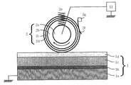
図1は、本発明に係る画像形成装置の一実施例の概略構成を示す。本実施例の画像形成装置100は、接触帯電方式、2成分接触現像方式、クリーナレス方式を採用した電子写真方式のレーザビームプリンタ(プリンタ)である。
【0032】
(1)プリンタの全体構成
先ず、図1を参照して、本実施例のプリンタ100の全体構成について説明する。
【0033】
(a)像担持体
プリンタ100は、像担持体として、回転ドラム型の電子写真感光体1(以下、「感光ドラム」と呼ぶ)を有する。本実施例において、感光ドラム1は、帯電特性が負帯電性の有機光導電休(OPC)であり、外径30mm、中心支軸を中心に130mm/secのプロセススピード(周速度)をもって矢示の反時計方向に回転駆動される。
【0034】
感光ドラム1は、図2に示すように、アルミニウム製シリンダ(導電性ドラム基体)1aの表面に、光の干渉を抑えて上層の接着性を向上させる下引き層1bと、光電荷発生層1cと、電荷輸送層1d(厚さ約20μm)との3層を下から順に塗り重ねた構成をしている。
【0035】
(b)帯電手段
プリンタ100は、感光ドラム1表面を一様に帯電処理する帯電手段として、接触帯電装置(接触帯電器)2を有する。本実施例において、接触帯電装置2は、帯電ローラ(ローラ帯電器)であり、感光ドラム1との間の微小ギャップにて生じる放電現象を利用して帯電する。
【0036】
帯電ローラ2は、芯金(支持部材)2aの両端部をそれぞれ軸受け部材(図示せず)により回転自在に保持されると共に、押圧ばね2eによって感光ドラム1に向かって付勢して、感光ドラム1の表面に対して所定の押圧力をもって圧接させている。これにより、帯電ローラ2は、感光ドラム1の回転に従動して回転する。感光ドラム1と帯電ローラ2との圧接部が帯電部(帯電ニップ部,接触部)aである。
【0037】
帯電ローラ2の芯金2aには、電源S1より所定の条件の帯電バイアス電圧が印加される。これにより、回転する感光ドラム1表面は、所定の極性・電位に接触帯電処理される。本実施例において、帯電ローラ2に対する帯電バイアス電圧は、直流電圧(Vdc)と交流電圧(Vac)とを重畳した振動電圧である。より具体的には、−500Vの直流電圧と、周波数1.3kHz、ピーク間電圧Vpp1.5kV、正弦波の交流電圧とを重畳した振動電圧である。この帯電バイアス電圧により、感光ドラム1表面は帯電ローラ2に印加した直流電圧と同じ−500V(暗電位Vd)に一様に接触帯電処理される。
【0038】
帯電ローラ2は長手長さ320mm、直径14mmである。また、図2の層構成模型図に示すように、芯金2aの外回りに、下層2bと、中間層2cと、表層2dとを下から順次に積層した3層構成である。下層2bは帯電音を低減するための発泡スポンジ層であり、表層2dは感光ドラム1上にピンホールなどの欠陥がある場合にもリークが発生するのを防止するために設けられた保護層である。より具体的には、本実施例の帯電ローラ2の仕様は下記の通りである。
【0039】
【0040】
図2に示すように、帯電ローラクリーニング部材2fが設けられている。本実施例では、帯電ローラクリーニング部材2fは、可撓性を持つクリーニングフィルムであり、具体的には厚さ25μmのポリイミドのフィルムである。この帯電ローラクリーニング部材2fは、帯電ローラ2の長手方向に対し平行に配置され、且つ、同長手方向に対し一定量の往復運動をする支持部材2gに一端を固定され、自由端側近傍の面において帯電ローラ2と接触ニップを形成するように配置されている。
【0041】
支持部材2gは、プリンタ100の駆動モーター(図示せず)により、ギア列を介して長手方向に対し一定量の往復運動駆動されて、帯電ローラ2の表層2dがクリーニングフィルム2fで摺擦される。これにより、帯電ローラ2の表面の付着物汚染(微粉トナー、外添剤など)の除去がなされる。
【0042】
(c)情報書き込み手段
プリンタ100は、帯電処理された感光ドラム1の面に静電潜像を形成する情報書き込み手段として露光手段たる露光装置3を有する。本実施例において、露光装置3は半導体レーザを用いたレーザビームスキャナである。レーザビームスキャナ3は、画像読み取り装置(図示せず)などのホスト処理装置からプリンタ側に送られた画像信号に対応して変調されたレーザ光Lを出力して、一様に帯電処理された回転する感光ドラム1の表面を、露光位置(露光部)bにおいてレーザ走査露光(イメージ露光)する。このレーザ走査露光により、感光ドラム1の表面のレーザ光Lで照射されたところの電位が低下し、回転する感光ドラム1の表面には、画像情報に対応した静電潜像が順次に形成されていく。
【0043】
(d)現像手段
プリンタ100は、感光ドラム1上の静電潜像に従ってトナーを供給し、静電潜像をトナー画像(現像剤像)として反転現像する現像手段として、現像装置(現像器)4を有する。本実施例においては、現像装置4はトナーとキヤリアからなる二成分現像剤による磁気ブラシを、感光ドラムに接触させながら現像を行う二成分接触現像方式を採用した現像装置である。
【0044】
現像装置4は、現像容器4a、現像剤担持体としての非磁性の現像スリーブ4bを備えている。現像スリーブ4bは、その外周面の一部を現像装置4の外部に露呈させて、現像容器4a内に回転可能に配置してある。現像スリーブ4b内には、非回転に固定してマグネットローラ4cが挿設されている。現像スリーブ4bに対向して、現像剤コーティングブレード4dが設けられている。現像容器4aは、二成分現像剤4eを収容しており、現像容器4a内の底部側には現像剤攪拌部材4fが配役されている。又、補給用トナーがトナーホッパー4gに収容されている。
【0045】
現像容器4a内の二成分現像剤(現像剤)4eは主に非磁性トナーと磁性キャリアとの混合物であり、現像剤攪拌部材4fにより攪拌される。本実施例において磁性キャリアの抵抗は約1013Ωcm、粒径(体積平均粒径:レーザ回折式粒度分布測定装置HEROS(日本電子製)を用いて、0.5〜350μmの範囲を32対数分割して測定し、体積50%メジアン径をもって体積平均粒径とする)は約40μmである。トナーは磁性キャリアとの摺擦により負極性に摩擦帯電される。
【0046】
現像スリーブ4bは、感光ドラム1との最近接距離(S−Dgap)を350μmに保持して感光ドラム1に近接対向配設される。この感光ドラム1と現像スリーブ4bとの対向部が現像部cである。
【0047】
現像スリーブ4bは、現像部cにおいて感光ドラム1の進行方向とは逆方向に回転駆動される。現像スリーブ4b内のマブネットローラ4cの磁力により、現像容器4a内の二成分現像剤4eの一部が現像スリーブ4bの外周面に磁気ブラシ層として吸着保持される。この磁気ブラシ層は、現像スリーブ4bの回転に伴い回転搬送され、現像剤コーティングブレード4dにより所定の薄層に整層され、現像部cにおいて感光ドラム1の面に対して接触して感光ドラム面を適度に摺擦する。
【0048】
現像スリーブ4bには、電源S2から所定の現像バイアスが印加される。本実施例において、現像スリーブ4bに対する現像バイアス電圧は、直流電圧(Vdc)と交流電圧(Vac)とを重畳した振動電圧である。より具体的には、−350Vの直流電圧と、周波数8.0kHz、ピーク間電圧1.8kV、矩形波の交流電圧とを重畳した振動電圧である。
【0049】
而して、回転する現像スリーブ4bの面に薄層としてコーティングされ、現像部cに搬送された現像剤4e中のトナーが、現像バイアスによる電界によって感光ドラム1の表面に静電潜像に対応して選択的に付着し、静電潜像がトナー画像として現像される。本実施例の場合、感光ドラム1の表面の露光明部にトナーが付着して静電潜像が反転現像される。
【0050】
この時、感光ドラム1上に現像されたトナーの帯電量は、温度23℃、絶対水分量10.5g/m3の環境下では凡そ−25μC/gである。
【0051】
現像部cを通過した現像スリーブ4b上の現像剤薄層は、引き続く現像スリーブ4bの回転に伴い現像容器4a内の現像剤溜り部に戻される。
【0052】
現像容器4a内の二成分現像剤4eのトナー濃度を、略一定の範囲内に維持するために、現像容器4a内の二成分現像剤4eのトナー濃度を、例えば、光学式トナー濃度センサーによって検知し、その検知情報に応じてトナーホッパー4gを駆動制御して、トナーホッパー4g内のトナーが現像容器4a内の二成分現像剤4eに補給される。二成分現像剤4eに補給されたトナーは、攪拌部材4fにより攪拌される。
【0053】
(e)転写手段・定着手段
プリンタ100は、転写手段として転写装置5を有する。本実施例においては、転写装置5は転写ローラである。転写ローラ5は、感光ドラム1に所定の押圧力をもって圧接され、その圧接ニップ部が転写部dである。この転写部dに絵紙機構部(図示せず)から所定の制御タイミングにて記録材Pが給送される。
【0054】
転写部dに給送された記録材Pは、回転する感光ドラム1と転写ローラ5との間に挟持されて搬送される。その間、転写ローラ5には電源S3からトナーの正規帯電極性である負極性とは逆極性である正極性の転写バイアス、本実施例では+2kVが印加される。これにより、転写部dを挟持搬送されていく記録材Pの表面に感光ドラム1の表面側のトナー画像が順次に静電転写されていく。
【0055】
転写部dを通ってトナー画像の転写を受けた記録材Pは、感光ドラム1の表面から順次に分離されて定着装置6へ搬送される。本実施例では、定着装置6は熱ローラ定着装置であり、この定着装置6により記録材Pはトナー画像の定着処理を受けて画像形成物(プリント、コピー)として出力される。
【0056】
(f)クリーナレスシステム、帯電補助手段および印加電圧制御
本実施例のプリンタ100は、所謂、クリーナレスシステムを採用しており、記録材Pに対するトナー画像転写後の感光ドラム1の表面に若干量残留する転写残トナー(残留トナー)を除去する専用のクリーニング装置を具備していない。
【0057】
転写後の感光ドラム1面上の転写残トナーは、引き続く感光ドラム1の回転に伴い帯電部a、露光部bを通って現像部cに搬送されて、現像装置4により現像同時クリーニングにて除去・回収される(クリーナレスシステム)。
【0058】
本実施例において、現像装置4の現像スリーブ4bは、上述のように現像部cにおいて感光ドラム1の表面の進行方向とは逆方向に回転させている。このような現像スリーブ4bの回転は、感光ドラム1上の転写残トナーの回収に有利である。
【0059】
感光ドラム1上の転写残トナーは露光部bを通るので、露光工程はその転写残トナー上からなされる。通常は、転写残トナーの量は少ないため、転写残トナー上から露光工程を行うことによる大きな影響は現れない。
【0060】
但し、上述したように、転写残トナーには帯電極性が正規極性のもの、逆極性のもの(反転トナー)、帯電量が少ないものが混在しており、その内の反転トナーや帯電量が少ないトナーが、帯電部aを通過する際に帯電ローラ2に付着すると、帯電ローラ2が許容以上にトナーにより汚染してしまい帯電不良を生じることがある(図3(領域▲1▼)参照)。
【0061】
又、感光ドラム1上の転写残トナーを、現像装置4により現像動作と同時に効果的に除去・回収するためには転写残トナーの帯電量が重要な因子となってくる。即ち、現像部cに持ち運ばれる感光ドラム1上の転写残トナーは、その帯電極性が正規極性であり、且つ、その帯電量が現像装置によって感光ドラム1の静電潜像を現像できるトナーの帯電量であることが好ましい。転写残トナーの帯電極性が反転している場合や帯電量が適切でない場合には、感光ドラム1上から現像装置4に除去・回収できず、不良画像の原因となる虞がある。
【0062】
そこで、帯電補助手段として、転写部dよりも感光ドラム1の回転方向下流側の位置において、感光ドラム1上の転写残トナーを均一化するための、残留トナー均一化手段(残留現像剤像均一化手段)8を設け、この残留トナー均一化手段8よりも感光ドラム1の回転方向下流側、且つ、帯電部aよりも感光ドラム1の回転方向上流側の位置において、転写残トナーの帯電極性を正規極性である負極性に揃えるためのトナー帯電量制御手段(現像剤帯電量制御手段)7を設ける。
【0063】
一般的に、転写部dで記録材Pに転写されずに感光ドラム1上に残留した転写残トナーは、反転トナーや帯電量が適切でないトナーが混在している。そこで、残留トナー均一化手段8により一度転写残トナーを除電し、次いでトナー帯電量制御手段7で再度転写残トナーを正規極性に帯電処理する。これにより、帯電ローラ2への転写残トナーの付着防止を効果的に成すと共に、現像装置4での転写残トナーの除去・回収を完全に行うことができる。そのため、転写残トナー像パターンのゴースト像の発生も厳に防止される。
【0064】
本実施例では、残留トナー均一化手段8及びトナー帯電量制御手段7は、適度の導電性を持ったブラシ状部材であり、ブラシ部を感光ドラム1の表面に接触させて配設されている。それぞれ残留トナー均一化手段8と感光ドラム1の表面との接触部f、トナー帯電量制御手段7と感光ドラム1の表面との接触部eを形成している。
【0065】
残留トナー均一化手段8には、電源S5より正極性の直流電圧が印加されており、トナー帯電量制御手段7には、電源S4より負極性の直流電圧が印加される。それぞれに印加される直流電圧の大きさは、装置内に設置した温湿度センサーにより検知した温度及び相対湿度より計算される絶対水分量により、図4(a),(b)に示すごとく変化させている。例えば、温度23℃、絶対水分量10.5g/m3の環境下においては、残留トナー均一化手段8には+250V、トナー帯電量制御手段7には−750Vの直流電圧がそれぞれ印加される。
【0066】
転写部dにおいて、記録材Pへのトナー画像の転写後に感光ドラム1上に残留する転写残トナーは、残留トナー均一化手段8と感光ドラム1との接触部fに至り、残留トナー均一化手段8によりその電荷量が0μC/g近傍で均一化される(図3(領域▲2▼)参照)。更に、残留トナー均一化手段8で均一化された感光ドラム1の表面上の転写残トナーは、トナー帯電量制御手段7と感光ドラム1との接触部eに至り、トナー帯電量制御手段7により、その帯電極性が正規極性である負極性に揃えられる(図3(領域▲3▼)参照)。
【0067】
転写残トナーの帯電極性を正規極性である負極性に揃えることにより、帯電ローラ2と感光ドラム1との接触部(帯電部)aで転写残トナーの上から感光ドラム1の表面上を帯電処理する際に、転写残トナーの感光ドラム1への鏡映力を大きくし、転写残トナーが帯電ローラ2へ付着するのを防止する。この為にトナー帯電量制御手段7により転写残トナーに与える帯電量は、現像時のトナー帯電量と比較すると約2倍以上であるのが好ましくし温度23℃、絶対水分量10.5g/m3の環境下では凡そ−50μC/gである。
【0068】
次に、現像工程における転写残トナーの回収について説明する。現像装置4は上述のように、現像と同時に転写残トナーを回収、清掃する。感光ドラム1上の静電潜像の現像に使用されるトナー帯電量(平均値)は、温度23℃、絶対水分量10.5g/m3の環境下においては凡そ−25μC/gである。
【0069】
感光ドラム1上の転写残トナーが現像装置4に十分に回収されるためには、現像装置4に到達する転写残トナーの帯電量が凡そ15〜35μC/gの範囲であることが好ましい。しかし、上述のように、帯電ローラ2へのトナー付着を防止するためにトナー帯電量制御手段7によって、−50μC/gと負極性に大きく帯電された転写残トナーは、現像装置4において回収させるためには除電を行う必要がある。
【0070】
ここで、帯電ローラ2には感光ドラム1表面を帯電処理するために、交流電圧(周波数1.3kHz、ピーク間電圧Vpp=1.5kV)が印加されている。この時、帯電ローラ2が感光ドラム1表面を帯電処理すると同時に、感光ドラム1上の転写残トナーが交流除電される。斯かる交流電圧条件において、凡そ−50μC/gであった転写残トナーの帯電量は、帯電部aの通過後に凡そ−30μC/gとなる。これにより、現像工程において、感光ドラム1上のトナーが付着されるべきではない部分(非画像部)に付着した転写残トナーは、現像装置4に回収される(図3(領域▲4▼)参照)。
【0071】
かくして、(i)感光ドラム1の回動に伴って転写部dから帯電部aへ搬送される転写残トナーの電荷量を、トナー帯電量制御手段7で正規極性である負極性に揃えて帯電処理して転写残トナーの帯電ローラ2への付着を防止し、(ii)帯電ローラ2で感光ドラム1を所定の電位に帯電すると同時に、トナー帯電量制御手段7で正規極性である負極性に帯電処理された転写残トナーの帯電量を、現像装置4で感光ドラム上の静電潜像を現像するのと同程度の帯電量に制御する。これにより、現像装置4での転写残トナーの回収が効率的に行われる。
【0072】
上述のようなクリーナレスシステム、特に現像同時クリーニング方式によれば、従来一般に用いられているようなクリーニング装置を特別に設ける必要がなく、又廃トナーを出さずに再利用することができ、メンテナンスの煩わしさ、装置の小型化に大きく貢献するばかりでなく、環境保全や資源の有効利用などの点で好ましい。
【0073】
しかしながら、本実施例で示したような画像形成装置を長時間使用した後には、残留トナー均一化手段8及びトナー帯電量制御手段7の表面への外添剤などが付着・蓄積や、直流電圧の長時間印加による通電劣化により抵抗が上昇してしまうため、転写残トナーヘのそれぞれの効果が低減し、転写残トナーの帯電量コントロールが不十分になってしまう。その結果、転写残トナーが帯電ローラ2表面に付着して帯電不良となったり、現像装置4に回収されずに感光ドラム1上を連れ回る虞がある。
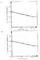
【0074】
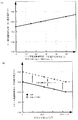
図5(a)は、絶対水分量10.6g/m3環境下における残留トナー均一化手段8に印加する電圧値と残留トナー均一化手段8から感光ドラム1に流れる電流量の関係について示したものである。図中点線で示した電流量(4μA)以上の電流が流れている場合には、転写残トナーを十分に除電することが可能であるが、点線で示した電流量(4μA)未満の場合には転写残トナーの除電が不安定になる。
【0075】
ここで、残留トナー均一化手段8に印加している電圧値は+250Vであり、画像形成装置使用初期においては、残留トナー均一化手段8から感光ドラム1に流れる電流量は約−13μAであるが、長期使用後(残留トナー均一化手段8に直流電圧を約100時間印加した後)には、残留トナー均一化手段8の抵抗値が上昇するために約3.5μAしか流れない。従って、長期使用後には残留トナー均一化手段8による転写残トナーの除電が不安定となる。
【0076】
なお、残留トナー均一化手段8に印加する電圧値を初期から十分に大きくした場合には、残留トナー均一化手段8がら感光ドラム1に流れ込む電流量が非常に大きくなりすぎるため、ドラムメモリーになる虞がある。
【0077】
同様に、図5(b)は、絶対水分量10.6g/m3環境下における残留トナー均一化手段8に印加する電圧値とトナー帯電量制御手段7から感光ドラム1に流れる電流量の関係について示したものである。図中点線で示した電流量(−8μA)以上の電流が流れている場合には、転写残トナーが帯電ローラ2に付着することを防止するのに十分な帯電量を付与することが可能であるが、点線で示した電流値(−8μA)未満の場合には転写残トナーに帯電量を十分付与することが不可能となり、転写残トナーの一部が帯電ローラ2表面に付着してしまう。
【0078】
ここで、トナー帯電量制御手段7に印加している電圧値は−750Vであり、画像形成装置使用初期においては、トナー帯電量制御手段7から感光ドラム1に流れる電流量は約−13μAであるが、長期使用後(トナー帯電量制御手段7に直流電圧を約100時間印加した後)には、トナー帯電量制御手段7の抵抗値が上昇するために約7.5μAしか流れない。従って、長期使用後にはトナー帯電量制御手段7による転写残トナーヘの帯電量付与が十分でなくなる。
【0079】
なお、トナー帯電量制御手段7に印加する電圧値を初期から十分に大きくした場合には、トナー帯電量制御手段7から感光ドラム1に流れ込む電流量が非常に大きくなりすぎるため、転写残トナーの帯電量が必要以上に大きくなり、帯電ローラ2で除電した後も現像装置4で回収不能な帯電量の転写残トナーが残ってしまう虞がある。
【0080】
更には、画像形成装置の長時間使用後には、現像装置4内に格納されているキヤリア表面に外添剤や微粉トナーが付着してしまうため、キヤリアの表面抵抗が上昇する。その結果、現像装置4により感光ドラム1表面に現像されるトナーの帯電量は全体的に若干低下すると共に、不均一化(ブロード化)してしまう。
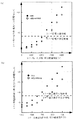
【0081】
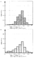
図10は、絶対水分量10.6g/m3環境下における現像装置4から感光ドラム1に現像されたトナーの帯電量分布を示している。(a)は初期の現像トナー帯電量分布であり、(b)がトナー帯電量制御手段7(あるいは残留トナー均一化手段8)に直流電圧を100時間印加したときの現像トナー帯電量分布である。初期の現像トナー帯電量分布は−20〜−30μC/gを中心としてある程度シャープな形状をしているのに対し、100時間には−20〜−30μC/g付近の帯電量のトナーの占める割合が低下しており、かつ帯電量が小さい(0〜−10μC/g)トナーや極性が反転しているトナーの占める割合が増加していることがわかる。その結果、画像形成装置の長期使用後では、転写残トナー中に反転トナーや帯電量の小さいトナーが初期に比べて増加してしまうことがわかる。
【0082】
そこで、本発明者は鋭意検討した結果、以下に示すような制御を行うことにより、上述のような画像形成装置を長期間にわたり使用する場合においても、転写残トナーの帯電量の適正なコントロールを行い、帯電ローラ2への付着、蓄積を防止し、転写残トナーを効率良く現像装置4により除去・回収することができると共に、帯電ローラ2により感光ドラム1を安定して帯電できることを見出した。
【0083】
つまり、本実施例においては、卜ナー帯電量制御手段7及び残留トナー均一化手段8に印加する直流電圧の制御値を、画像形成装置の使用量としてのトナー帯電量制御手段7及び残留トナー均一化手段8への電圧印加積算時間に従って1次関数的に連続して増加させる制御を行った。
【0084】
ここで、電圧印加積算時間は、使用量検知手段10でカウントする。具体的には画像形成装置内に内蔵されたCPUで、トナー帯電量制御手段7及び残留トナー均一化手段8に直流電圧が印加されている時間をカウントし、随時メモリに積算させていく。
【0085】
更に、メモリに随時積算された電圧印加積算時間に応じて、決められた関係(本実施例の場合には1次関数)に基づき制御手段10(CPU)により印加電圧の制御値を計算し、トナー帯電量制御手段7及び残留トナー均一化手段8にそれぞれ印加する。
【0086】
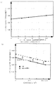
図6(a)は、本実施例の画像形成装置を絶対水分量が10.6g/m3の環境下で使用した場合に、残留トナー均一化手段8の電圧印加積算時間と、各タイミングにおける残留トナー均一化手段8に印加する直流電圧の制御値との関係を示したものである。ここで残留トナー均一化手段8に印加する直流電圧の制御値は、電圧印加積算時間に対して1次関数的に増加させて制御を行っている。
【0087】
つまり、あるタイミング(t;電圧印加積算時間)における残留トナー均一化手段8に印加する直流電圧の制御値(Vdc▲1▼(t))は、
Vdc▲1▼(t)=Vdc▲1▼(0)十50×(t/100)…(式▲1▼)
で表すことができる。ここでVdc▲1▼(0)は初期の残留トナー均一化手段8に印加する直流電圧の制御値であり、図4(a)に示すように画像形成装置内の絶対水分量により決定される(絶対水分量10.6g/m3環境下では+250V)。
【0088】
例えば、残留トナー均一化手段8の電圧印加積算時間が100時間の時には、残留トナー均一化手段8に印加する直流電圧の制御値は、初期+250Vであるのに対して+300Vとなる。これは、図5(a)に示すように、積算時間が100時間の残留トナー均一化手段8は、通電劣化などにより抵抗値が上昇し、残留トナー均一化手段8から感光ドラム1に流れ込む電流量が低下してしまう。具体的には、残留トナー均一化手段8に印加する直流電圧の制御値が+250Vである場合、残留トナー均一化手段8から感光ドラム1に流れ込む電流量は、初期で+6μAであるのに対して、100時間後では+3.5μAとなってしまう。このために転写残トナーを十分除電することが不可能となる。
【0089】
ここで、転写残トナーを十分除電するためには、残留トナー均一化手段8から感光ドラム1に流れ込む電流量が初期と同じ程度になるような印加電圧の制御値にする必要があり、図5(a)の関係から残留卜ナー均一化手段8に+300V程度印加する必要があることがわかる。
【0090】
このように、残留トナー均一化手段8に印加する直流電圧の制御値を、残留トナー均一化手段8の電圧印加積算時間に従って連続的に増加させるような制御を行うことにより、長期間に渡り安定して転写残トナーを除電することが可能となる。
【0091】
図6(b)は、残留トナー均一化手段8の場合と同様に、本実施例の画像形成装置を絶対水分量が10.6g/m3の環境下で使用した場合に、トナー帯電量制御手段7の電圧印加積算時間と、各タイミングにおけるトナー帯電量制御手段7に印加する直流電圧の制御値との関係を示したものである。ここでトナー帯電量制御手段7に印加する直流電圧の制御値は、電圧印加積算時間に対して1次関数的に増加させて制御を行っている。
【0092】
トナー帯電量制御手段7の場合にも、あるタイミング(t;電圧印加積算時間)におけるトナー帯電量制御手段7に印加する直流電圧の制御値(Vdc▲2▼(t))は、
Vdc▲2▼(t)=Vdc▲2▼(0)十(−100)×(t/100)…(式▲2▼)
で表すことができる。ここでVdc▲2▼(0)は初期のトナー帯電量制御手段7に印加する直流電圧の制御値であり、図4(b)に示すように画像形成装置内の絶対水分量により決定される(絶対水分量10.6g/m3環境下では−750V)。
【0093】
例えば、トナー帯電量制御手段7の電圧印加積算時間が100時間の時には、トナー帯電量制御手段7に印加する直流電圧の制御値は、初期−750Vであるのに対して−850Vとなる。これも残留トナー均一化手段8の場合と同様であり、図5(a)の関係が示すとおりである。つまり、トナー帯電量制御手段7の電圧印加積算時間が100時間の時に、転写残トナーの帯電ローラ2への付着を防止するのに必要な帯電量を転写残トナーに与えるためには、図5(b)の関係からトナー帯電量制御手段7に−850V程度印加する必要があることがわかる。
【0094】
このように、トナー帯電量制御手段7に印加する直流電圧の制御値を、トナー帯電量制御手段7の電圧印加積算時間に従って連続的に増加させるような制御を行うことにより、長期間に渡り安定して転写残トナーの帯電量をコントロールすることが可能となる。
【0095】
なお、トナー帯電量制御手段7に印加する直流電圧の極性は、帯電ローラ2に印加する直流電圧の極性、つまり感光ドラム1表面を帯電処理する極性と同じであることから、トナー帯電量制御手段7は感光ドラム1表面の帯電前処理を行う役目も果たしている。実際絶対水分量10.6g/m3環境下で、トナー帯電量制御手段7に直流電圧−850Vを印加した場合、トナー帯電量制御手段7によって感光ドラム1表面は凡そ−350Vに帯電される。
【0096】
このため、画像形成装置を長期にわたり使用した後に、外添剤の付着や通電劣化により帯電ローラ2の抵抗値が上昇し帯電ローラ2の感光ドラム1への帯電処理能力が低下した場合に、トナー帯電量制御手段7に印加する直流電圧を大きくすることで、感光ドラム1表面の安定した帯電処理を行うことも可能になる。
【0097】
以上、本実施例によれば、トナー帯電量制御手段7及び残留トナー均一化手段8に印加する直流電圧の制御値を、画像形成装置の使用量としてのトナー帯電量制御手段7及び残留トナー均一化手段8への電圧印加積算時間に従って連続的に増加させる制御を行うことにより、画像形成装置の長期使用後において、トナー帯電量制御手段7及び残留トナー均一化手段8が外添剤などの蓄積や通電劣化した場合でも、転写残トナーの帯電量を片付制御することが可能となり、帯電ローラ2への転写残トナーの付着や現像装置4での転写残トナー回収不良を防止することができる。更には、帯電ローラ2が劣化した場合でも、感光ドラム1表面の帯電処理を均一・安定に行うことができる。
【0098】
なお、本実施例で示したように、トナー帯電量制御手段トナー7及び残留トナー均一化手段8の両方について上記の制御を行うことが最も好ましいが、どちらか片側のみについて実施するだけでも良い。
【0099】
トナー帯電量制御手段トナー7及び残留トナー均一化手段8は、固定のブラシ状部材に限定されるものではなく、ブラシ回転体,弾性ローラ,シート状部材など任意の形態の部材であっても良い。
【0100】
接触帯電部材2は、帯電ローラの他に、ファーブラシ,フェルトなどの形状・材質のものも使用可能である。また、各種材質のものの組み合わせでより適切な弾性、導電性、表面性、耐久性のものを得ることができる。
【0101】
像担持体は、表面の体積抵抗が109〜1014Ωcmの電荷注入層を設けた直接注入帯電性のものであっても良い。電荷注入層を用いていない場合でも、例えば電荷輸送層が上記の抵抗範囲にある場合も同等の効果が得られる。表層の体積抵抗が1013Ωcmであるアモルファスシリコン感光体でも良い。
【0102】
〈実施例2〉
次に、本発明の他の実施例について説明する。本実施例の画像形成装置(プリンタ)の基本構成は実施例1のものと同様である。従って、実施例1のプリンタ100と同一の機能、構成を有する要素には同一の符号を付し、詳しい説明は省略する。
【0103】
実施例1では、トナー帯電量制御手段7及び残留トナー均一化手段8に印加する直流電圧の制御値を、画像形成装置の使用量としてのトナー帯電量制御手段7及び残留トナー均一化手段8への電圧印加積算時間に従って1次関数的に連続して増加させる制御を行った。
【0104】
しかし実施例1の形態においては、直流電圧の制御値を電圧印加積算時間に従って1次関数的に連続して増加させるため、トナー帯電量制御手段7及び残留トナー均一化手段8が通電劣化していない状況においても高い直流電圧を印加させることになり、結果的に若干ではあるが通電劣化を加速させてしまう場合がある。
【0105】
そこで、本実施例では、電圧印加積算時間のタイミング別に、直流電圧を増加させない期間や直流電圧の増加量を実施例1に比べて大きくする期間を設けた。
【0106】
本実施例おける残留トナー均一化手段8及びトナー帯電量制御手段7の電圧印加積算時間と、残留トナー均一化手段8及びトナー帯電量制御手段7に印加する直流電圧の制御値との関係を、それぞれ図8の(a),(b)に示す(絶対水分量10.6g/m3環境下における制御値)。
【0107】
残留トナー均一化手段8については、図8(a)に示すように、あるタイミング(t;電圧印加積算時間)における残留トナー均一化手段8に印加する直流電圧の制御値(Vdc▲1▼(t))は、
(i)積算時間;0〜40(h)
Vdc▲1▼(t)=+250V(一定) …(式▲3▼)
(ii)積算時間;40〜80(h)
Vdc▲1▼(t)=Vdc▲1▼(0)+50×((t−40)/40)…(式▲4▼)
(iii)積算時間;80(h)以上
Vdc▲1▼(t)=(Vdc▲1▼(0)+50)+75×((t−80)/20)…(式▲5▼)
で表すことができる。ここでVdc▲1▼(0)は初期の残留トナー均一化手段8に印加する直流電圧の制御値であり、図8(a)に示すように画像形成装置内の絶対水分量により決定される(絶対水分量10.6g/m3環境下では+250V)。
【0108】
トナー帯電量制御手段7については、図8(b)に示すように、あるタイミング(t;電圧印加積算時間)におけるトナー帯電量制御手段7に印加する直流電圧の制御値(Vdc▲2▼(t))は、
(i)積算時間;0〜40(h)
Vdc▲2▼(t)=−750V(一定)…(式▲6▼)
(ii)積算時間;40〜80(h)
Vdc▲2▼(t)=Vdc▲2▼(0)+(−50)×((t−40)/40)…(式▲7▼)
(iii)積算時間;80(h)以上
Vdc▲2▼(t)=
(Vdc▲2▼(0)−50+(−100)×((t−80)/20)…(式▲8▼)で表すことができる。ここでVdc▲2▼(0)は初期のトナー帯電量制御手段7に印加する直流電圧の制御値であり、図8(b)に示すように画像形成装置内の絶対水分量により決定される(絶対水分量10.6g/m3環境下では−750V)。
【0109】
以上、本実施例によれば、トナー帯電量制御手段7及び残留トナー均一化手段8に印加する直流電圧の制御値を、トナー帯電量制御手段7及び残留トナー均一化手段8への電圧印加積算時間に基づいて段階的に増加させる制御を行うことにより、トナー帯電量制御手段7及び残留トナー均一化手段8の通電劣化を極力抑制しつつ、実施例1と同様の効果を得ることができる。
【0110】
〈実施例3〉
更に、本発明の他の実施例について説明する。本実施例の画像形成装置(プリンタ)の基本構成は実施例1のものと同様である。従って、実施例1のプリンタ100と同一の機能、構成を有する要素には同一の符号を付し、詳しい説明は省略する。
【0111】
実施例1では、トナー帯電量制御手段7及び残留トナー均一化手段8に印加する直流電圧の制御値を、画像形成装置の使用量としてのトナー帯電量制御手段7及び残留トナー均一化手段8への電圧印加積算時間に従って1次関数的に連続して増加させる制御を、画像形成装置の使用環境にかかわらず同じように実施していた(図6(b),図7(b)参照)。
【0112】
しかし、実際には画像形成装置の使用環境によって、現像装置4で現像される現像トナーおよび転写残トナーの特性(帯電量分布)が若干異なる。つまり低湿環境下(絶対水分量0.8g/m3)では、現像装置4で現像される現像トナーの帯電量分布が、初期(図10(a)参照)と長期使用後(図11(a)参照)でほとんど変わらないのに対し、高湿環境下(絶対水分量21.6g/m3)では、帯電量分布がブロードになると共に、極性の反転したトナーが増加する(図11(b)参照)。
【0113】
つまり、実施例1の形態では、直流電圧制御値の電圧印加積算時間に対する増加量が、画像形成装置の使用環境によらず一定であったため、特に高湿環境(絶対水分量が大きい環境)で、トナー帯電量制御手段7及び残留トナー均一化手段8に印加する直流電圧が不足気味になり、転写残トナーのコントロールが十分に行えず、転写残トナーの帯電ローラ2への付着や、現像装置4での転写残トナー回収不良が発生する虞がある。
【0114】
そこで、本実施例では、画像形成装置内に雰囲気の温湿度を検知する環境センサー11を設け、そこから計算される絶対米分量によって、電圧印加積算時間による直流電圧の増加量を変化させた(図12参照)。
【0115】
本実施例おける残留トナー均一化手段8及びトナー帯電量制御手段7の、使用環境における印加高圧の制御値変化(それぞれの絶対水分量に対して初期と100時間後を示してある)を図9の(a),(b)に示す。
【0116】
残留トナー均一化手段8について、図9(a)に基づいて説明すれば、
(i)絶対水分量0.8g/m3のとき
初期;+300V → 100時間後;+300V (変化量0V)
(ii)絶対水分量10.6g/m3のとき
初期;+250V → 100時間後;+300V (変化量50V)
(iii)絶対水分量21.6g/m3のとき
初期;+200V → 100時間後;+300V (変化量100V)
になるように、印加する直流電圧の制御値を各絶対水分量において随時増加させる。増加させる方法は実施例1,実施例2どちらの方式でも良い。
【0117】
トナー帯電量制御手段7についても同様で、図9(b)に基づいて説明すれば、
(i)絶対水分量0.8g/m3のとき
初期;−800V → 100時間後;−800V (変化量0V)
(ii)絶対水分量10.6g/m3のとき
初期;−750V → 100時間後;−850V (変化量100V)
(iii)絶対水分量21.6g/m3のとき
初期;−700V → 100時間後;−900V (変化量200V)
になるように、印加する直流電圧の制御値を各絶対水分量において随時増加させる。増加させる方法は実施例1,実施例2どちらの方式でも良い。
【0118】
以上、本実施例によれば、トナー帯電量制御手段7及び残留トナー均一化手段8に印加する直流電圧の制御値を、トナー帯電量制御手段7及び残留トナー均一化手段8への電圧印加積算時間に基づいて増加させる制御を行う場合において、トナー帯電量制御手段7及び残留トナー均一化手段8の電圧印加積算時間による直流電圧の増加量を、画像形成装置を使用する環境(具体的には絶対水分量)に応じて変化させることで、画像形成装置の使用環境によらず、実施例1と同様の効果を得ることができる。
【0119】
〈その他〉
1)本発明の実施例における、トナーの電荷量μC/gは、所謂ブローオフ法により測定した。
【0120】
2)情報書き込み手段としての露光手段3は、実施例のレーザビームスキャナに限られず、LEDアレイ、蛍光灯等の光源と液晶シャッターとの組み合わせ等の他のデジタル露光装置であってもよいし、原稿画像を結像投影するアナログ露光装置であってもよい。
【0121】
3)像担持体1は、静電記録誘電体であってもよい。この場合は該誘電体面を所定の極性・電位に一様に帯電した後、除電針アレイ・電子銃等の除電手段(情報書き込み手段)で選択的に除電して画像情報の静電潜像を書き込み形成する。
【0122】
4)受像部材として転写材Pは、中間転写ドラムや中間転写ベルト等の中間転写体であってもよい。この場合、中間転写体からシートのような転写材へ再度像転写が行なわれる。
【0123】
5)接触帯電装置2や現像装置4に印加するバイアスの交流電圧の波形としては、正弦波、矩形波、三角波等的義使用可能である。交流バイアスは、例えば直流電源を周期的にON,OFFすることによって形成された矩形波の電圧を含む。
【0124】
【発明の効果】
以上説明したように、トナー帯電量制御手段及び残留トナー均一化手段などの帯電補助手段に印加する直流電圧の制御値を、画像形成装置の使用量を検知する手段により検知した情報、例えば帯電補助手段に印加する電圧印加時間の積算値などに従って、制御手段により変化させる制御を行うことにより、画像形成装置の長期使用後において、帯電補助手段が外添剤などの蓄積や通電劣化した場合でも、転写残現像剤(転写残トナー)の帯電量を十分制御することが可能となり、接触帯電装置への転写残現像剤の付着や現像装置での転写残現像剤回収不良を防止することができる。更には、接触帯電装置自体が劣化した場合でも、像担持体表面の帯電処理を均一・安定に行うことができる。
【図面の簡単な説明】
【図1】本発明に係る画像形成装置の一実施例の概略構成を示す模型図である。
【図2】図1の画像形成装置が備える感光ドラム及び帯電ローラの層構成を示す模型図である。
【図3】本発明に係る画像形成装置のクナーナレスシステムについて説明するための図である。
【図4】(a)は残留トナー均一化手段の絶対水分量に対する印加電圧の関係を示す関係図である。
(b)はトナー帯電量制御手段の絶対水分量に対する印加電圧の関係を示す関係図である。
【図5】(a)は残留トナー均一化手段の印加電圧と感光ドラムに流れ込む電流量の関係を示す関係図である。
(b)はトナー帯電量制御手段の印加電圧と感光ドラムに流れ込む電流量の関係を示す関係図である。
【図6】(a)は実施例1の画像形成装置において、残留トナー均一化手段の印加電圧制御値と電圧印加積算時間の関係を示す関係図である。
(b)は実施例1の画像形成装置において、残留トナー均一化手段の印加電圧制御値と絶対水分量の関係を示す関係図である。
【図7】(a)は実施例1の画像形成装置において、トナー帯電量制御手段の印加電圧制御値と電圧印加積算時間の関係を示す関係図である。
(b)は実施例1の画像形成装置において、トナー帯電量制御手段の印加電圧制御値と絶対水分量の関係を示す関係図である。
【図8】(a)は実施例2の画像形成装置において、残留トナー均一化手段の印加電圧制御値と電圧印加積算時間の関係を示す関係図である。
(b)は実施例2の画像形成装置において、トナー帯電量制御手段の印加電圧制御値と電圧印加積算時間の関係を示す関係図である。
【図9】(a)は実施例3の画像形成装置において、残留トナー均一化手段の印加電圧制御値と電庄印加積算時間の関係を示す関係図である。
(b)は実施例3の画像形成装置において、トナー帯電量制御手段の印加電圧制御値と電圧印加積算時間の関係を示す関係図である。
【図10】(a)は本発明に係る画像形成装置において、使用初期の現像装置により現像される現像トナーの帯電量分布を示す関係図である。
(b)は本発明に係る画像形成装置において、長期使用後の現像装置により現像される現像トナーの帯電量分布を示す関係図である。
【図11】(a)は本発明に係る画像形成装置において、低湿環境下で、長期使用後の現像装置により現像される現像トナーの帯電量分布を示す関係図である。
(b)は本発明に係る画像形成装置において、高湿環境下で、長期使用後の現像装置により現像される現像トナーの帯電量分布を示す関係図である。
【図12】実施例3に係る画像形成装置の概略構成を示す模型図である。
【符号の説明】
1 感光ドラム(像担持体)
2 帯電ローラ(帯電手段)
3 レーザビームスキャナ(露光手段)
4 現像装置(現像手段)
5 転写ローラ(転写手段)
6 定着装置
7 トナー帯電量制御手段(帯電補助手段)
8 残留トナー均一化手段(帯電補助手段)
10 CPU(使用量検知手段および制御手段)
11 環境検知センサー(絶対水分量検知手段)[0001]
TECHNICAL FIELD OF THE INVENTION
The present invention relates to an image forming apparatus using an electrophotographic method, an electrostatic recording method, or the like, and more particularly, to an image forming apparatus such as a copying machine, a printer, and a facsimile.
[0002]
[Prior art]
2. Description of the Related Art Conventionally, an image forming apparatus such as a copying machine, a printer, and a facsimile using an electrophotographic method generally includes an electrophotographic photosensitive member (photosensitive member) which is a rotating drum type image carrier, and the photosensitive member is provided with a predetermined polarity and potential. Charging device (charging process) for uniformly and uniformly charging, an exposure device (exposure process) as information writing means for forming an electrostatic latent image on the charged photoconductor, and an electrostatic latent image formed on the photoconductor. A developing device (developing process) for visualizing an image as a developer image (toner image) with toner as a developer, a transfer device (transfer process) for transferring the toner image from the surface of the photoconductor to a recording material such as paper, A cleaning device (cleaning process) for removing the toner (residual developer and transfer residual toner) slightly remaining on the photoconductor after the transfer process and cleaning the photoconductor surface, and a fixing device for fixing the toner image on the recording material Fixing process) includes a like, by repeating the photosensitive member as an electrophotographic process (charging step, exposing step, developing step, transferring step, cleaning iv) is subjected is applied for image formation.
[0003]
The toner remaining on the photoreceptor after the transfer process is removed from the surface of the photoreceptor by the cleaning device, and is collected in the cleaning device and becomes waste toner. However, it is desirable that such waste toner does not appear from the viewpoint of environmental conservation and effective use of resources.
[0004]
Therefore, an image forming apparatus has been proposed in which untransferred toner collected by a cleaning device, so-called waste toner, is returned to a developing device and reused.
[0005]
In addition, the cleaning device is eliminated, and the transfer residual toner on the photoreceptor after the transfer process is removed and collected from the photoreceptor by "simultaneous development" in the developing device, and is reused. Has been proposed.
[0006]
In the development simultaneous cleaning, the transfer residual toner on the photoreceptor after the transfer process is collected in the developing device at the time of the subsequent development process. That is, the photoreceptor to which the transfer residual toner has adhered is continuously charged and exposed to form an electrostatic latent image, and a fogging bias (the DC voltage applied to the developing device and the surface of the photoreceptor) during the developing process of the electrostatic latent image By the fogging potential difference (Vback), which is a potential difference between potentials, the transfer residual toner remaining on the portion not to be developed (non-image portion) of the transfer residual toner remaining on the photoreceptor surface is removed and collected by the developing device. How to
[0007]
According to this method, since the transfer residual toner is collected in the developing device and reused for the development of the electrostatic latent image in the next and subsequent steps, waste toner is eliminated, and troublesome maintenance is reduced. Can be. Further, the present invention is also advantageous in miniaturizing a cleaner-less toner image forming apparatus.
[0008]
In the case of a cleanerless image forming apparatus employing the simultaneous development and cleaning described above, when a contact charging device is used as a charging device that contacts the photoconductor and charges the surface of the photoconductor, transfer residual toner on the photoconductor is reduced. When passing through the contact nip (charging portion) between the photoreceptor and the contact charging device, toner in the transfer residual toner, in particular, the toner whose charging polarity is reversed to the opposite polarity to the normal polarity, adheres to the contact charging device. May be. As a result, the contact charging device may be unduly contaminated with toner, which may cause charging failure.
[0009]
That is, the toner as the developer contains a small amount of toner whose charge polarity is originally inverted to the opposite polarity to the normal polarity. Further, even if the toner has a normal charge polarity, there is a toner whose charge polarity is reversed due to an influence of a transfer bias or a peeling discharge, or a toner whose charge amount is reduced due to charge elimination.
[0010]
For this reason, the transfer residual toner includes a toner having a normal charge polarity, a toner having a reverse polarity, and a toner having a small charge amount. When passing through the contact nip portion (charging portion), the toner adheres to the contact charging device.
[0011]
Also, in order to remove and collect the transfer residual toner on the photoreceptor by simultaneous cleaning with development, the charge polarity of the transfer residual toner on the photoreceptor carried through the charging unit to the development unit is a normal polarity. Also, it is necessary that the charge amount is a charge amount of the toner that can develop the electrostatic latent image on the photoconductor by the developing device. Inverted toner and toner with an inappropriate charge amount cannot be removed and collected from the photoreceptor to the developing device, and may cause a defective image.
[0012]
In order to prevent toner from adhering to the contact charging device, on the photoreceptor where the charging polarity transported from the transfer unit to the charging unit is normal polarity, reverse polarity, or low in charge amount It is necessary to charge the transfer residual toner to the normal polarity to make the charge polarity uniform, and to make the charge amount uniform.
[0013]
Therefore, conventionally, as a charging assisting unit, a toner charging amount control unit that is located upstream of the contact charging device in the moving direction of the photoconductor and downstream of the transfer unit and charges the transfer residual toner, A transfer residual toner equalizing means (residual toner uniforming means), which is located upstream of the control means and downstream of the transfer means, and which equalizes transfer residual toner on the photoconductor, is brought into contact with the surface of the photoconductor. This problem is solved by applying a constant DC voltage to the residual toner equalizing means and the toner charge amount controlling means (for example, see Patent Documents 1 and 2).
[0014]
That is, the residual toner remaining on the photoreceptor after the transfer is made uniform by the residual toner uniforming means, and the uniformed transfer residual toner on the photoreceptor is charged to the normal polarity by the toner charge amount control means. Then, at the same time as charging the surface of the photoreceptor with the contact charging device, the transfer residual toner charged by the toner charge amount control means is charged to an appropriate charge amount so as to be removed and recovered by the simultaneous cleaning in the developing device. And collected by a developing device.
[Patent Document 1]
JP 2001-215798 A
[Patent Document 2]
JP 2001-215799 A
[0015]
[Problems to be solved by the invention]
However, when the above-described image forming apparatus is used for a long period of time, toner and external additives accumulate and become contaminated in charging auxiliary means such as a residual toner uniformizing means and a toner charge amount controlling means. The means itself may be deteriorated, the control of the charge amount of the transfer residual toner becomes insufficient, and the adhesion of the transfer residual toner to the contact charging device may not be prevented.
[0016]
In addition, a small amount of toner, external additives, etc. accumulate and contaminate the contact charging device, and the contact charging device itself deteriorates, which lowers the charging ability of the photoreceptor surface by the contact charging device. However, there is a fear that charging failure may occur.
[0017]
SUMMARY OF THE INVENTION It is an object of the present invention to provide an image forming apparatus that prevents transfer residual toner from adhering to a contact charging device and stably and uniformly charges the surface of a photoreceptor even after the image forming apparatus has been used for a long time. Is to do.
[0018]
[Means for Solving the Problems]
The present invention is an image forming apparatus having the following configuration.
[0019]
(1) an image carrier, charging means for charging the image carrier at a contact portion for forming an electrostatic image on the image carrier, and the image carrier charged by the charging means. An information writing unit for forming an electrostatic latent image, a developing unit for supplying a developer to the electrostatic latent image formed on the image carrier to visualize the electrostatic latent image, and a transfer unit for transferring the visualized developer image to a transfer material And a developer remaining on the surface of the image carrier that is not transferred by the transfer unit and has at least one charging auxiliary unit to which a DC voltage is applied to the image carrier after transfer. In an image forming apparatus using a cleanerless system that collects the toner in the developing device, a use amount detecting unit that detects a use amount of the image forming device, and the charging auxiliary unit according to a detection result of the use amount detection unit. Variable DC voltage applied to at least one of them An image forming apparatus characterized by comprising a Gosuru control means.
[0020]
(2) The image forming apparatus according to (1), wherein the image forming apparatus has two charging auxiliary units.
[0021]
(3) The image forming apparatus according to (2), wherein the polarities of the DC voltages applied to the charging auxiliary means are different from each other.
[0022]
(4) Of the charging auxiliary means, the DC voltage applied to the charging auxiliary member disposed closest to the transfer means has a polarity opposite to that of the charging means, and The image forming apparatus according to (3), wherein the polarity of the DC voltage applied to the charging assisting unit disposed close to the charging unit is the same as that of the charging unit.
[0023]
(5) The image forming apparatus according to any one of (1) to (4), wherein the charging assisting unit is disposed between the transfer unit and the charging unit in contact with the image carrier.
[0024]
(6) The image forming apparatus according to any one of (1) to (5), wherein the charging auxiliary unit is a member made of a brush.
[0025]
(7) The image forming apparatus according to any one of (1) to (6), wherein the charging unit is a charging roller.
[0026]
(8) The image forming apparatus according to any one of (1) to (7), wherein the information writing unit is an exposure unit.
[0027]
(9) The usage amount detected by the usage amount detecting means is an integrated value of an application time of a voltage applied to the charging means or the charging assisting means, wherein (1) to (8). Image forming device.
[0028]
(10) The relationship between the control amount of the DC voltage applied to the charging auxiliary means and the amount of use of the image forming apparatus differs depending on the absolute moisture content of the environmental atmosphere in which the image forming apparatus is used. The image forming apparatus according to (9).
[0029]
<Operation>
The control value of the DC voltage applied to the charging auxiliary means such as the toner charge amount control means and the residual toner uniforming means is information detected by the means for detecting the amount of use of the image forming apparatus, for example, the voltage applied to the charging auxiliary means. By performing control by the control means in accordance with the integrated value of the time and the like, even if the charging auxiliary means accumulates external additives and the like and degrades electricity after long-term use of the image forming apparatus, the transfer residual developer (transfer residual It is possible to sufficiently control the charge amount of the residual toner), and it is possible to prevent the transfer residual developer from adhering to the contact charging device and to prevent the transfer residual developer from being poorly collected in the developing device. Further, even when the contact charging device itself is deteriorated, the charging process on the surface of the image carrier can be uniformly and stably performed.
[0030]
BEST MODE FOR CARRYING OUT THE INVENTION
Hereinafter, the image forming apparatus according to the present invention will be described in more detail with reference to the drawings.
[0031]
<Example 1>
FIG. 1 shows a schematic configuration of an embodiment of an image forming apparatus according to the present invention. The image forming apparatus 100 of the present embodiment is an electrophotographic laser beam printer (printer) employing a contact charging system, a two-component contact developing system, and a cleanerless system.
[0032]
(1) Overall configuration of printer
First, an overall configuration of a printer 100 according to the present embodiment will be described with reference to FIG.
[0033]
(A) Image carrier
The printer 100 has a rotating drum type electrophotographic photosensitive member 1 (hereinafter, referred to as “photosensitive drum”) as an image carrier. In the present embodiment, the photosensitive drum 1 is a negatively chargeable organic photoconductive layer (OPC) having an outer diameter of 30 mm and a process speed (peripheral speed) of 130 mm / sec around a central support shaft. Is rotated counterclockwise.
[0034]
As shown in FIG. 2, the photosensitive drum 1 has a subbing layer 1b on the surface of an aluminum cylinder (conductive drum base) 1a for suppressing the interference of light and improving the adhesiveness of an upper layer, and a photocharge generating layer 1c. And a charge transport layer 1d (thickness: about 20 μm).
[0035]
(B) Charging means
The printer 100 includes a contact charging device (contact charger) 2 as a charging unit for uniformly charging the surface of the photosensitive drum 1. In the present embodiment, the contact charging device 2 is a charging roller (roller charger), and charges using a discharge phenomenon generated in a minute gap between the photosensitive drum 1 and the charging roller.
[0036]
The charging roller 2 rotatably holds both ends of a cored bar (supporting member) 2a by bearing members (not shown), and urges the photosensitive drum 1 toward the photosensitive drum 1 by a pressing spring 2e. 1 is pressed against the surface with a predetermined pressing force. As a result, the charging roller 2 rotates following the rotation of the photosensitive drum 1. The pressure contact portion between the photosensitive drum 1 and the charging roller 2 is a charging portion (charging nip portion, contact portion) a.
[0037]
A charging bias voltage under predetermined conditions is applied to the core metal 2a of the charging roller 2 from a power supply S1. Thus, the surface of the rotating photosensitive drum 1 is contact-charged to a predetermined polarity and potential. In the present embodiment, the charging bias voltage for the charging roller 2 is an oscillating voltage obtained by superimposing a DC voltage (Vdc) and an AC voltage (Vac). More specifically, it is an oscillating voltage obtained by superimposing a -500 V DC voltage, a frequency of 1.3 kHz, a peak-to-peak voltage Vpp of 1.5 kV, and a sine wave AC voltage. With this charging bias voltage, the surface of the photosensitive drum 1 is uniformly contact-charged to -500 V (dark potential Vd), which is the same as the DC voltage applied to the charging roller 2.
[0038]
The charging roller 2 has a longitudinal length of 320 mm and a diameter of 14 mm. As shown in the schematic diagram of the layer structure in FIG. 2, the lower layer 2b, the intermediate layer 2c, and the surface layer 2d are sequentially laminated from the bottom around the outer periphery of the cored bar 2a. The lower layer 2b is a foamed sponge layer for reducing charging noise, and the surface layer 2d is a protective layer provided to prevent a leak from occurring even when there is a defect such as a pinhole on the photosensitive drum 1. is there. More specifically, the specifications of the charging roller 2 of the present embodiment are as follows.
[0039]
[0040]
As shown in FIG. 2, a charging roller cleaning member 2f is provided. In the present embodiment, the charging roller cleaning member 2f is a cleaning film having flexibility, specifically, a polyimide film having a thickness of 25 μm. The charging roller cleaning member 2f is arranged in parallel with the longitudinal direction of the charging roller 2 and has one end fixed to a supporting member 2g that reciprocates a fixed amount in the longitudinal direction, and has a surface near the free end side. Are arranged so as to form a contact nip with the charging roller 2.
[0041]
The support member 2g is driven by a drive motor (not shown) of the printer 100 to reciprocate a fixed amount in the longitudinal direction via a gear train, and the surface layer 2d of the charging roller 2 is rubbed with the cleaning film 2f. . As a result, contaminant contamination (fine powder toner, external additives, etc.) on the surface of the charging roller 2 is removed.
[0042]
(C) Information writing means
The printer 100 includes an exposure device 3 as an exposure unit as an information writing unit that forms an electrostatic latent image on the surface of the charged photosensitive drum 1. In the present embodiment, the exposure device 3 is a laser beam scanner using a semiconductor laser. The laser beam scanner 3 outputs a laser beam L modulated according to an image signal sent from a host processing device such as an image reading device (not shown) to the printer, and is uniformly charged. The surface of the rotating photosensitive drum 1 is subjected to laser scanning exposure (image exposure) at an exposure position (exposure portion) b. By this laser scanning exposure, the potential of the surface of the photosensitive drum 1 irradiated with the laser beam L is reduced, and an electrostatic latent image corresponding to image information is sequentially formed on the surface of the rotating photosensitive drum 1. To go.
[0043]
(D) developing means
The printer 100 has a developing device (developing device) 4 as a developing unit that supplies toner according to the electrostatic latent image on the photosensitive drum 1 and reversely develops the electrostatic latent image as a toner image (developer image). In this embodiment, the developing device 4 is a developing device adopting a two-component contact developing method in which a magnetic brush made of a two-component developer composed of a toner and a carrier is developed while being brought into contact with a photosensitive drum.
[0044]
The developing device 4 includes a developing container 4a and a non-magnetic developing sleeve 4b as a developer carrier. The developing sleeve 4b is rotatably disposed in the developing container 4a with a part of the outer peripheral surface being exposed to the outside of the developing device 4. A magnet roller 4c is inserted and fixed in the developing sleeve 4b so as not to rotate. A developer coating blade 4d is provided opposite to the developing sleeve 4b. The developing container 4a contains a two-component developer 4e, and a developer stirring member 4f is disposed on the bottom side inside the developing container 4a. The replenishment toner is stored in the toner hopper 4g.
[0045]
The two-component developer (developer) 4e in the developing container 4a is mainly a mixture of a non-magnetic toner and a magnetic carrier, and is stirred by the developer stirring member 4f. In this embodiment, the resistance of the magnetic carrier is about 10 Thirteen Ωcm, particle size (volume average particle size: measured using a laser diffraction type particle size distribution analyzer, HEROS (manufactured by JEOL Ltd.), by dividing the range of 0.5 to 350 μm into 32 logarithms, and measuring the volume with a 50% median diameter. The average particle size is about 40 μm. The toner is triboelectrically charged to a negative polarity by rubbing with the magnetic carrier.
[0046]
The developing sleeve 4b is disposed in close proximity to the photosensitive drum 1 while maintaining the closest distance (S-Dgap) to the photosensitive drum 1 at 350 μm. The facing portion between the photosensitive drum 1 and the developing sleeve 4b is a developing portion c.
[0047]
The developing sleeve 4b is driven to rotate in a direction opposite to the direction in which the photosensitive drum 1 advances in the developing section c. A part of the two-component developer 4e in the developing container 4a is adsorbed and held as a magnetic brush layer on the outer peripheral surface of the developing sleeve 4b by the magnetic force of the mabnet roller 4c in the developing sleeve 4b. The magnetic brush layer is rotated and conveyed in accordance with the rotation of the developing sleeve 4b, is formed into a predetermined thin layer by the developer coating blade 4d, and is brought into contact with the surface of the photosensitive drum 1 in the developing section c to contact the photosensitive drum surface. Rub moderately.
[0048]
A predetermined developing bias is applied to the developing sleeve 4b from the power supply S2. In this embodiment, the developing bias voltage for the developing sleeve 4b is an oscillating voltage obtained by superimposing a DC voltage (Vdc) and an AC voltage (Vac). More specifically, it is an oscillating voltage obtained by superimposing a -350 V DC voltage, a frequency of 8.0 kHz, a peak-to-peak voltage of 1.8 kV, and a rectangular wave AC voltage.
[0049]
Thus, the toner in the developer 4e, which is coated as a thin layer on the surface of the rotating developing sleeve 4b and conveyed to the developing section c, corresponds to the electrostatic latent image on the surface of the photosensitive drum 1 by the electric field generated by the developing bias. And the electrostatic latent image is developed as a toner image. In the case of the present embodiment, the toner adheres to the exposed light portion on the surface of the photosensitive drum 1, and the electrostatic latent image is reversely developed.
[0050]
At this time, the charge amount of the toner developed on the photosensitive drum 1 is 23 ° C. and the absolute water content is 10.5 g / m 2. 3 Is approximately -25 μC / g.
[0051]
The developer thin layer on the developing sleeve 4b that has passed the developing section c is returned to the developer reservoir in the developing container 4a with the subsequent rotation of the developing sleeve 4b.
[0052]
In order to maintain the toner concentration of the two-component developer 4e in the developing container 4a within a substantially constant range, the toner concentration of the two-component developer 4e in the developing container 4a is detected by, for example, an optical toner concentration sensor. Then, the toner hopper 4g is driven and controlled according to the detection information, and the toner in the toner hopper 4g is supplied to the two-component developer 4e in the developing container 4a. The toner supplied to the two-component developer 4e is stirred by the stirring member 4f.
[0053]
(E) Transfer means and fixing means
The printer 100 has a transfer device 5 as a transfer unit. In this embodiment, the transfer device 5 is a transfer roller. The transfer roller 5 is pressed against the photosensitive drum 1 with a predetermined pressing force, and the press-contact nip portion is a transfer portion d. The recording material P is fed to the transfer section d at a predetermined control timing from a picture paper mechanism section (not shown).
[0054]
The recording material P fed to the transfer unit d is conveyed while being sandwiched between the rotating photosensitive drum 1 and the transfer roller 5. During this time, a positive transfer bias (+2 kV in this embodiment) is applied to the transfer roller 5 from the power supply S3 from the power supply S3, which has a polarity opposite to the negative polarity, which is the normal charge polarity of the toner. As a result, the toner image on the front side of the photosensitive drum 1 is sequentially electrostatically transferred to the surface of the recording material P that is nipping and conveying the transfer portion d.
[0055]
The recording material P to which the toner image has been transferred through the transfer unit d is sequentially separated from the surface of the photosensitive drum 1 and is conveyed to the fixing device 6. In the present embodiment, the fixing device 6 is a heat roller fixing device, and the recording material P is subjected to a toner image fixing process by the fixing device 6 and is output as an image formed product (print, copy).
[0056]
(F) Cleanerless system, auxiliary charging means and applied voltage control
The printer 100 of this embodiment employs a so-called cleanerless system, and is dedicated to removing transfer residual toner (residual toner) slightly remaining on the surface of the photosensitive drum 1 after the transfer of the toner image onto the recording material P. Does not have a cleaning device.
[0057]
The untransferred toner on the surface of the photosensitive drum 1 after the transfer is conveyed to the developing unit c through the charging unit a and the exposing unit b with the subsequent rotation of the photosensitive drum 1, and is removed by the developing device 4 by simultaneous cleaning with development. -Collected (cleanerless system).
[0058]
In the present embodiment, the developing sleeve 4b of the developing device 4 is rotated in the developing unit c in the direction opposite to the traveling direction of the surface of the photosensitive drum 1 as described above. Such rotation of the developing sleeve 4b is advantageous for collecting the transfer residual toner on the photosensitive drum 1.
[0059]
Since the transfer residual toner on the photosensitive drum 1 passes through the exposure section b, the exposure process is performed on the transfer residual toner. Usually, since the amount of the transfer residual toner is small, there is no significant effect due to performing the exposure step on the transfer residual toner.
[0060]
However, as described above, the transfer residual toner includes a toner having a normal polarity, a toner having a reverse polarity (inverted toner), and a toner having a small charge amount, of which the inverted toner and the charge amount are small. If the toner adheres to the charging roller 2 while passing through the charging section a, the charging roller 2 may be contaminated by the toner more than allowed, resulting in poor charging (see FIG. 3 (region (1))).
[0061]
Further, in order to effectively remove and collect the transfer residual toner on the photosensitive drum 1 simultaneously with the developing operation by the developing device 4, the charge amount of the transfer residual toner is an important factor. That is, the transfer residual toner on the photosensitive drum 1 carried to the developing section c has a regular charging polarity, and the amount of charge of the toner is such that the developing device can develop the electrostatic latent image on the photosensitive drum 1. The charge amount is preferably. When the charge polarity of the transfer residual toner is reversed or the charge amount is not appropriate, the transfer residual toner cannot be removed and collected from the photosensitive drum 1 to the developing device 4, which may cause a defective image.
[0062]
Therefore, as a charging assisting means, at a position downstream of the transfer section d in the rotation direction of the photosensitive drum 1, a residual toner equalizing means (uniform residual developer image uniforming) for equalizing transfer residual toner on the photosensitive drum 1. A charging polarity of the transfer residual toner at a position downstream of the residual toner equalizing unit 8 in the rotational direction of the photosensitive drum 1 and upstream of the charging unit a in the rotational direction of the photosensitive drum 1. Charge amount control means (developer charge amount control means) 7 for adjusting the negative polarity to a normal polarity.
[0063]
Generally, the untransferred toner remaining on the photosensitive drum 1 without being transferred to the recording material P at the transfer portion d includes a reversal toner and a toner having an inappropriate charge amount. Therefore, the residual toner is once discharged by the residual toner equalizing means 8, and then the residual toner is charged to the normal polarity again by the toner charge amount control means 7. As a result, it is possible to effectively prevent the transfer residual toner from adhering to the charging roller 2 and completely remove and collect the transfer residual toner in the developing device 4. Therefore, generation of a ghost image of the transfer residual toner image pattern is strictly prevented.
[0064]
In the present embodiment, the residual toner equalizing means 8 and the toner charge amount controlling means 7 are brush-like members having appropriate conductivity, and are arranged with the brush portion in contact with the surface of the photosensitive drum 1. . A contact portion f between the residual toner uniforming means 8 and the surface of the photosensitive drum 1 and a contact portion e between the toner charge amount control means 7 and the surface of the photosensitive drum 1 are formed.
[0065]
A positive DC voltage is applied to the residual toner uniforming means 8 from the power supply S5, and a negative DC voltage is applied to the toner charge amount control means 7 from the power supply S4. The magnitude of the DC voltage applied to each is changed as shown in FIGS. 4 (a) and 4 (b) according to the absolute water content calculated from the temperature and relative humidity detected by the temperature / humidity sensor installed in the apparatus. ing. For example, at a temperature of 23 ° C. and an absolute water content of 10.5 g / m 3 In this environment, a DC voltage of +250 V is applied to the residual toner uniforming means 8 and a DC voltage of -750 V is applied to the toner charge amount controlling means 7.
[0066]
In the transfer section d, the transfer residual toner remaining on the photosensitive drum 1 after the transfer of the toner image onto the recording material P reaches the contact portion f between the residual toner equalizing means 8 and the photosensitive drum 1, and the residual toner uniforming means 8, the charge amount is made uniform in the vicinity of 0 μC / g (see FIG. 3 (region (2))). Further, the transfer residual toner on the surface of the photosensitive drum 1 uniformized by the residual toner uniforming means 8 reaches a contact portion e between the toner charge amount control means 7 and the photosensitive drum 1, and the toner charge amount control means 7 The charging polarity is adjusted to the negative polarity, which is the normal polarity (see FIG. 3 (region (3))).
[0067]
By setting the charge polarity of the transfer residual toner to the negative polarity, which is the normal polarity, the surface of the photosensitive drum 1 is charged from above the transfer residual toner at the contact portion (charging portion) a between the charging roller 2 and the photosensitive drum 1. In this case, the transfer force of the transfer residual toner to the photosensitive drum 1 is increased to prevent the transfer residual toner from attaching to the charging roller 2. For this reason, the charge amount given to the transfer residual toner by the toner charge amount control means 7 is preferably about twice or more as compared with the toner charge amount at the time of development, at a temperature of 23 ° C. and an absolute water content of 10.5 g / m 2. 3 Is approximately -50 μC / g under the environment of (1).
[0068]
Next, the recovery of the transfer residual toner in the developing step will be described. As described above, the developing device 4 collects and cleans the transfer residual toner simultaneously with the development. The toner charge amount (average value) used for developing the electrostatic latent image on the photosensitive drum 1 is a temperature of 23 ° C. and an absolute water content of 10.5 g / m 2. 3 Is approximately -25 μC / g.
[0069]
In order for the transfer residual toner on the photosensitive drum 1 to be sufficiently collected in the developing device 4, it is preferable that the charge amount of the transfer residual toner reaching the developing device 4 be in a range of about 15 to 35 μC / g. However, as described above, the transfer residual toner charged to a large negative value of −50 μC / g by the toner charge amount control unit 7 in order to prevent the toner from adhering to the charging roller 2 is collected in the developing device 4. Therefore, it is necessary to remove static electricity.
[0070]
Here, an AC voltage (frequency: 1.3 kHz, peak-to-peak voltage Vpp = 1.5 kV) is applied to the charging roller 2 to charge the surface of the photosensitive drum 1. At this time, the transfer residual toner on the photosensitive drum 1 is subjected to an alternating current charge elimination at the same time as the charging roller 2 charges the surface of the photosensitive drum 1. Under such AC voltage conditions, the charge amount of the transfer residual toner, which was about -50 .mu.C / g, becomes about -30 .mu.C / g after passing through the charging section a. As a result, in the developing step, the transfer residual toner attached to the portion (non-image portion) where the toner on the photosensitive drum 1 should not be attached is collected by the developing device 4 (FIG. 3 (region {circle around (4))). reference).
[0071]
Thus, (i) the charge amount of the transfer residual toner conveyed from the transfer portion d to the charging portion a with the rotation of the photosensitive drum 1 is adjusted by the toner charge amount control means 7 to the negative polarity which is the normal polarity. (Ii) charging the photosensitive drum 1 to a predetermined potential by the charging roller 2 and, at the same time, setting the toner charge amount control means 7 to a negative polarity of a normal polarity. The charge amount of the transfer-residual toner that has been subjected to the charge processing is controlled to the same charge amount as when the developing device 4 develops the electrostatic latent image on the photosensitive drum. Thereby, the transfer residual toner is efficiently collected in the developing device 4.
[0072]
According to the cleaner-less system as described above, particularly the simultaneous development cleaning method, there is no need to provide a special cleaning device, which is generally used in the past, and it can be reused without generating waste toner. Not only greatly contributes to the inconvenience and downsizing of the apparatus, but is also preferable in terms of environmental conservation and effective use of resources.
[0073]
However, after the image forming apparatus as shown in the present embodiment is used for a long time, the external additives and the like adhere to and accumulate on the surfaces of the residual toner equalizing means 8 and the toner charge amount controlling means 7, For this reason, the resistance increases due to the deterioration of the energization due to the long-time application, and the respective effects on the transfer residual toner are reduced, and the charge amount control of the transfer residual toner becomes insufficient. As a result, there is a possibility that the transfer residual toner adheres to the surface of the charging roller 2 to cause a charging failure, or the toner remains around the photosensitive drum 1 without being collected by the developing device 4.
[0074]
FIG. 5A shows an absolute water content of 10.6 g / m. 3 The relationship between the voltage applied to the residual toner uniforming means 8 and the amount of current flowing from the residual toner uniforming means 8 to the photosensitive drum 1 under an environment is shown. When a current equal to or more than the current amount (4 μA) indicated by the dotted line in the figure flows, it is possible to sufficiently remove the residual toner after transfer, but when the current amount is smaller than the current amount (4 μA) indicated by the dotted line. In this case, the charge removal of the transfer residual toner becomes unstable.
[0075]
Here, the voltage value applied to the residual toner uniforming means 8 is +250 V, and the amount of current flowing from the residual toner uniforming means 8 to the photosensitive drum 1 is about -13 μA in the early stage of use of the image forming apparatus. After long-term use (after applying a DC voltage to the residual toner uniforming means 8 for about 100 hours), only about 3.5 μA flows because the resistance value of the residual toner uniforming means 8 increases. Therefore, after long-term use, the charge removal of the transfer residual toner by the residual toner uniforming means 8 becomes unstable.
[0076]
If the voltage value applied to the residual toner uniforming means 8 is sufficiently large from the beginning, the amount of current flowing into the photosensitive drum 1 from the residual toner uniforming means 8 becomes too large, so that a drum memory is provided. There is a fear.
[0077]
Similarly, FIG. 5B shows an absolute water content of 10.6 g / m 2. 3 The relationship between the voltage value applied to the residual toner uniforming means 8 and the amount of current flowing from the toner charge control means 7 to the photosensitive drum 1 under the environment is shown. When a current equal to or greater than the current amount (-8 μA) indicated by the dotted line in the drawing flows, it is possible to provide a sufficient charge amount to prevent the transfer residual toner from adhering to the charging roller 2. However, when the current value is less than the current value (−8 μA) indicated by the dotted line, it becomes impossible to sufficiently impart a charge amount to the transfer residual toner, and a part of the transfer residual toner adheres to the surface of the charging roller 2. .
[0078]
Here, the voltage value applied to the toner charge amount control means 7 is -750 V, and the amount of current flowing from the toner charge amount control means 7 to the photosensitive drum 1 is about -13 .mu.A in the early stage of use of the image forming apparatus. However, after long-term use (after a DC voltage is applied to the toner charge control means 7 for about 100 hours), only about 7.5 μA flows because the resistance of the toner charge control means 7 increases. Therefore, after long-term use, the toner charge amount control means 7 does not provide sufficient charge to the transfer residual toner.
[0079]
When the voltage value applied to the toner charge amount control means 7 is sufficiently large from the beginning, the amount of current flowing from the toner charge amount control means 7 to the photosensitive drum 1 becomes too large, so The charge amount becomes unnecessarily large, and there is a possibility that the transfer residual toner having a charge amount that cannot be collected by the developing device 4 remains even after the charge roller 2 removes the charge.
[0080]
Further, after the image forming apparatus has been used for a long time, the external additive and the fine powder toner adhere to the surface of the carrier stored in the developing device 4, so that the surface resistance of the carrier increases. As a result, the charge amount of the toner developed on the surface of the photosensitive drum 1 by the developing device 4 is slightly reduced as a whole, and becomes non-uniform (broadened).
[0081]
FIG. 10 shows an absolute water content of 10.6 g / m. 3 4 shows a charge amount distribution of toner developed on the photosensitive drum 1 from the developing device 4 under an environment. (A) is the initial charge distribution of the developed toner, and (b) is the charge distribution of the developed toner when a DC voltage is applied to the toner charge control means 7 (or the residual toner uniforming means 8) for 100 hours. . The initial development toner charge amount distribution has a somewhat sharp shape centered at -20 to -30 [mu] C / g, whereas the toner occupies a charge amount around -20 to -30 [mu] C / g in 100 hours. It can be seen that the ratio of the toner having a small charge amount (0 to -10 μC / g) and the toner of which the polarity is inverted are increasing. As a result, it can be seen that after the image forming apparatus has been used for a long period of time, the amount of the reversal toner or the toner having a small charge amount in the transfer residual toner increases as compared with the initial amount.
[0082]
Accordingly, the present inventor has conducted intensive studies, and as a result, by performing the following control, even when the above-described image forming apparatus is used for a long period of time, it is possible to appropriately control the charge amount of the transfer residual toner. It was found that the toner was prevented from adhering and accumulating on the charging roller 2, the transfer residual toner could be efficiently removed and collected by the developing device 4, and the photosensitive drum 1 could be stably charged by the charging roller 2.
[0083]
That is, in the present embodiment, the control value of the DC voltage applied to the toner charge amount control means 7 and the residual toner uniformity means 8 is changed to the toner charge amount control means 7 and the residual toner uniformity Control to continuously increase linearly according to the voltage application integration time to the conversion means 8.
[0084]
Here, the accumulated voltage application time is counted by the usage amount detecting means 10. Specifically, a CPU built in the image forming apparatus counts the time during which the DC voltage is applied to the toner charge amount control means 7 and the residual toner uniformity means 8 and accumulates the time in the memory as needed.
[0085]
Further, a control value of the applied voltage is calculated by the control means 10 (CPU) based on a determined relationship (a linear function in the case of the present embodiment) in accordance with the voltage application integration time accumulated as needed in the memory, The voltage is applied to the toner charge amount control means 7 and the residual toner uniformity means 8, respectively.
[0086]
FIG. 6A shows that the image forming apparatus of this embodiment has an absolute water content of 10.6 g / m 2. 3 3 shows the relationship between the integrated time of voltage application of the residual toner uniforming means 8 and the control value of the DC voltage applied to the residual toner uniforming means 8 at each timing when used in the above environment. Here, the control value of the DC voltage applied to the residual toner uniforming means 8 is controlled by increasing it linearly with respect to the integrated voltage application time.
[0087]
That is, at a certain timing (t; voltage application integration time), the control value (Vdc <1> (t)) of the DC voltage applied to the residual toner uniforming means 8 is:
Vdc (1) (t) = Vdc (1) (0) + 50 × (t / 100) (Equation (1))
Can be represented by Here, Vdc (1) (0) is a control value of the DC voltage applied to the initial residual toner uniforming means 8, and is determined by the absolute water content in the image forming apparatus as shown in FIG. (10.6 g / m absolute water content) 3 + 250V under environment).
[0088]
For example, when the integrated voltage application time of the residual toner uniforming means 8 is 100 hours, the control value of the DC voltage applied to the residual toner uniforming means 8 is +300 V, compared to +250 V in the initial stage. This is because, as shown in FIG. 5 (a), the residual toner uniforming means 8 having an integration time of 100 hours has a resistance value which increases due to deterioration of energization and the like, and the current flowing into the photosensitive drum 1 from the residual toner uniforming means 8 The amount will decrease. Specifically, when the control value of the DC voltage applied to the residual toner uniforming means 8 is +250 V, the amount of current flowing into the photosensitive drum 1 from the residual toner uniforming means 8 is +6 μA at the beginning. After 100 hours, it becomes +3.5 μA. For this reason, it is impossible to sufficiently remove the charge of the transfer residual toner.
[0089]
Here, in order to sufficiently remove electricity from the transfer residual toner, it is necessary to set the control value of the applied voltage so that the amount of current flowing from the residual toner uniforming means 8 to the photosensitive drum 1 becomes substantially equal to the initial value. It can be seen from the relationship (a) that it is necessary to apply about +300 V to the residual toner uniforming means 8.
[0090]
In this way, by performing control such that the control value of the DC voltage applied to the residual toner uniforming means 8 is continuously increased in accordance with the voltage application integration time of the residual toner uniforming means 8, the control is stabilized over a long period of time. As a result, the transfer residual toner can be discharged.
[0091]
FIG. 6B shows that the image forming apparatus of this embodiment has an absolute water content of 10.6 g / m 3 3 shows the relationship between the voltage application integration time of the toner charge amount control means 7 and the control value of the DC voltage applied to the toner charge amount control means 7 at each timing when used in the environment described in FIG. Here, the control value of the DC voltage applied to the toner charge amount control means 7 is controlled by increasing it linearly with respect to the voltage application integrated time.
[0092]
Also in the case of the toner charge amount control means 7, the control value (Vdc (2) (t)) of the DC voltage applied to the toner charge amount control means 7 at a certain timing (t: voltage application integration time) is
Vdc <2> (t) = Vdc <2> (0) 10 (-100) * (t / 100) (Equation (2))
Can be represented by Here, Vdc (2) (0) is a control value of the DC voltage applied to the initial toner charge amount control means 7, and is determined by the absolute water content in the image forming apparatus as shown in FIG. (10.6 g / m absolute water content) 3 (-750V under the environment).
[0093]
For example, when the voltage application integration time of the toner charge amount control means 7 is 100 hours, the control value of the DC voltage applied to the toner charge amount control means 7 is -850V, compared with -750V in the initial stage. This is also the same as the case of the residual toner uniforming means 8, as shown in the relationship of FIG. In other words, when the voltage application integrated time of the toner charge amount control means 7 is 100 hours, in order to provide the transfer residual toner with a charge amount necessary to prevent the transfer residual toner from adhering to the charging roller 2, FIG. From the relationship (b), it can be seen that it is necessary to apply a voltage of about -850 V to the toner charge amount control means 7.
[0094]
As described above, by performing control such that the control value of the DC voltage applied to the toner charge amount control means 7 is continuously increased in accordance with the voltage application integration time of the toner charge amount control means 7, the control is performed over a long period of time. Thus, the charge amount of the transfer residual toner can be controlled.
[0095]
Since the polarity of the DC voltage applied to the toner charge amount control means 7 is the same as the polarity of the DC voltage applied to the charging roller 2, that is, the polarity for charging the surface of the photosensitive drum 1, the toner charge amount control means Reference numeral 7 also serves to perform a pre-charging process on the surface of the photosensitive drum 1. Actual water content of 10.6g / m 3 When a DC voltage of -850 V is applied to the toner charge amount controller 7 under the environment, the surface of the photosensitive drum 1 is charged to approximately -350 V by the toner charge amount controller 7.
[0096]
For this reason, after the image forming apparatus has been used for a long period of time, if the resistance of the charging roller 2 increases due to the attachment of an external additive or deterioration due to energization, and the charging processing ability of the charging roller 2 to the photosensitive drum 1 decreases, the toner By increasing the DC voltage applied to the charge amount control means 7, a stable charging process on the surface of the photosensitive drum 1 can be performed.
[0097]
As described above, according to the present embodiment, the control value of the DC voltage applied to the toner charge amount control means 7 and the residual toner uniformity means 8 is changed to the toner charge amount control means 7 and the residual toner uniformity as the usage amount of the image forming apparatus. After the image forming apparatus has been used for a long period of time, the toner charge amount control means 7 and the residual toner uniforming means 8 can accumulate external additives and the like after the long-term use of the image forming apparatus. Even if the power supply deteriorates, the charge amount of the transfer residual toner can be controlled to be cleared, thereby preventing the transfer residual toner from adhering to the charging roller 2 and the transfer residual toner collection failure in the developing device 4. . Further, even when the charging roller 2 is deteriorated, the charging process on the surface of the photosensitive drum 1 can be performed uniformly and stably.
[0098]
As described in the present embodiment, it is most preferable to perform the above-described control on both the toner charge amount control means toner 7 and the residual toner uniformity means 8, but it is also possible to perform the control only on one of the two sides.
[0099]
The toner charge amount controlling means 7 and the residual toner uniforming means 8 are not limited to fixed brush-like members, but may be members of any form such as a brush rotating body, an elastic roller, and a sheet-like member. .
[0100]
The contact charging member 2 may be formed of a material or a shape such as a fur brush or a felt in addition to the charging roller. In addition, more appropriate elasticity, conductivity, surface properties and durability can be obtained by combining various materials.
[0101]
The image carrier has a surface volume resistance of 10 9 -10 14 It may be of a direct injection charging type provided with a charge injection layer of Ωcm. Even when the charge injection layer is not used, the same effect can be obtained, for example, when the charge transport layer is in the above-described resistance range. Surface volume resistance is 10 Thirteen An amorphous silicon photoreceptor of Ωcm may be used.
[0102]
<Example 2>
Next, another embodiment of the present invention will be described. The basic configuration of the image forming apparatus (printer) of the present embodiment is the same as that of the first embodiment. Therefore, elements having the same functions and configurations as those of the printer 100 according to the first embodiment are denoted by the same reference numerals, and detailed description thereof will be omitted.
[0103]
In the first embodiment, the control value of the DC voltage applied to the toner charge amount control means 7 and the residual toner uniformity means 8 is transmitted to the toner charge amount control means 7 and the residual toner uniformity means 8 as the usage of the image forming apparatus. Was controlled so as to increase continuously as a linear function in accordance with the voltage application integration time.
[0104]
However, in the embodiment of the first embodiment, the control value of the DC voltage is continuously increased in a linear function according to the voltage application integration time. Even in such a situation, a high DC voltage is applied, and as a result, the conduction deterioration may be slightly accelerated.
[0105]
Therefore, in the present embodiment, a period during which the DC voltage is not increased and a period during which the amount of increase in the DC voltage is increased as compared with the first embodiment are provided for each timing of the voltage application integration time.
[0106]
The relationship between the voltage application integration time of the residual toner uniforming means 8 and the toner charge amount control means 7 and the control value of the DC voltage applied to the residual toner uniformity means 8 and the toner charge amount control means 7 in this embodiment is as follows. 8 (a) and 8 (b) respectively (absolute water content 10.6 g / m 3 Control value under environment).
[0107]
As shown in FIG. 8A, the control value (Vdc <1>) of the DC voltage applied to the residual toner uniforming unit 8 at a certain timing (t; integrated time of voltage application) is applied to the residual toner uniforming unit 8. t))
(I) Integrated time; 0 to 40 (h)
Vdc (1) (t) = + 250 V (constant) (Equation (3))
(Ii) Integrated time: 40 to 80 (h)
Vdc-1 (t) = Vdc-1 (0) + 50 × ((t-40) / 40) (Equation (4))
(Iii) Integrated time; 80 (h) or more
Vdc (1) (t) = (Vdc (1) (0) +50) + 75 × ((t−80) / 20) (Equation (5))
Can be represented by Here, Vdc (1) (0) is a control value of the DC voltage applied to the initial residual toner uniforming means 8 and is determined by the absolute water content in the image forming apparatus as shown in FIG. (10.6 g / m absolute water content) 3 + 250V under environment).
[0108]
As shown in FIG. 8B, the toner charge amount control means 7 controls the DC voltage at a certain timing (t; integrated voltage application time). t))
(I) Integrated time; 0 to 40 (h)
Vdc (2) (t) =-750 V (constant) (Equation (6))
(Ii) Integrated time: 40 to 80 (h)
Vdc 2 (t) = Vdc 2 (0) + (− 50) × ((t−40) / 40) (Formula 7)
(Iii) Integrated time; 80 (h) or more
Vdc <2> (t) =
(Vdc (2) (0) −50 + (− 100) × ((t−80) / 20) (Equation (8)) where Vdc (2) (0) is the initial toner. The control value of the DC voltage applied to the charge amount control means 7 is determined by the absolute water content in the image forming apparatus as shown in FIG. 3 (-750V under the environment).
[0109]
As described above, according to this embodiment, the control value of the DC voltage applied to the toner charge amount control means 7 and the residual toner uniformity means 8 is integrated with the voltage applied to the toner charge amount control means 7 and the residual toner uniformity means 8. By performing the control of increasing stepwise based on time, it is possible to obtain the same effect as in the first embodiment while minimizing the power supply deterioration of the toner charge amount control means 7 and the residual toner uniforming means 8.
[0110]
<Example 3>
Further, another embodiment of the present invention will be described. The basic configuration of the image forming apparatus (printer) of the present embodiment is the same as that of the first embodiment. Therefore, elements having the same functions and configurations as those of the printer 100 according to the first embodiment are denoted by the same reference numerals, and detailed description thereof will be omitted.
[0111]
In the first embodiment, the control value of the DC voltage applied to the toner charge amount control means 7 and the residual toner uniformity means 8 is transmitted to the toner charge amount control means 7 and the residual toner uniformity means 8 as the usage of the image forming apparatus. The control to continuously increase linearly according to the voltage application integration time is performed in the same manner regardless of the use environment of the image forming apparatus (see FIGS. 6B and 7B).
[0112]
However, in actuality, the characteristics (charge amount distribution) of the developed toner and the transfer residual toner developed by the developing device 4 are slightly different depending on the use environment of the image forming apparatus. In other words, under a low humidity environment (absolute moisture content 0.8 g / m 3 11), the charge amount distribution of the developing toner developed by the developing device 4 hardly changes between the initial stage (see FIG. 10A) and after long-term use (see FIG. 11A), while the high humidity environment Bottom (21.6 g / m absolute water content) 3 ), The charge amount distribution becomes broad and the amount of toner whose polarity is inverted increases (see FIG. 11B).
[0113]
That is, in the embodiment of the first embodiment, the amount of increase in the DC voltage control value with respect to the integrated voltage application time is constant regardless of the use environment of the image forming apparatus. In addition, the DC voltage applied to the toner charge amount control means 7 and the residual toner uniforming means 8 tends to be insufficient, and the control of the transfer residual toner cannot be performed sufficiently. There is a possibility that the transfer residual toner collection failure in No. 4 may occur.
[0114]
Therefore, in the present embodiment, the environment sensor 11 for detecting the temperature and humidity of the atmosphere is provided in the image forming apparatus, and the amount of increase in the DC voltage due to the cumulative voltage application time is changed by the absolute rice content calculated from the environment sensor 11 ( See FIG. 12).
[0115]
FIG. 9 shows changes in the control value of the applied high pressure in the use environment of the residual toner uniforming means 8 and the toner charge amount control means 7 in the present embodiment (the initial and 100 hours after each absolute water content). (A) and (b) of FIG.
[0116]
The residual toner uniforming means 8 will be described with reference to FIG.
(I) Absolute water content 0.8 g / m 3 When
Initial: + 300V → After 100 hours; + 300V (change amount 0V)
(Ii) Absolute moisture content 10.6 g / m 3 When
Initial: + 250V → After 100 hours; + 300V (change amount 50V)
(Iii) Absolute water content 21.6 g / m 3 When
Initial: + 200V → After 100 hours; + 300V (change amount 100V)
The control value of the DC voltage to be applied is increased as needed at each absolute water content. The method of increasing the number may be either the embodiment 1 or the embodiment 2.
[0117]
The same applies to the toner charge amount control means 7, which will be described with reference to FIG.
(I) Absolute water content 0.8 g / m 3 When
Initial: -800V → After 100 hours; -800V (change amount 0V)
(Ii) Absolute moisture content 10.6 g / m 3 When
Initial: -750V → After 100 hours; -850V (change amount 100V)
(Iii) Absolute water content 21.6 g / m 3 When
Initial: -700V → After 100 hours; -900V (Change amount 200V)
The control value of the DC voltage to be applied is increased as needed at each absolute water content. The method of increasing the number may be either the embodiment 1 or the embodiment 2.
[0118]
As described above, according to this embodiment, the control value of the DC voltage applied to the toner charge amount control means 7 and the residual toner uniformity means 8 is integrated with the voltage applied to the toner charge amount control means 7 and the residual toner uniformity means 8. In the case of performing the control for increasing based on time, the amount of increase of the DC voltage due to the voltage application integration time of the toner charge amount control unit 7 and the residual toner uniforming unit 8 is determined by the environment (specifically, the environment where the image forming apparatus is used). The effect similar to that of the first embodiment can be obtained irrespective of the use environment of the image forming apparatus by changing the value in accordance with the absolute water content.
[0119]
<Others>
1) In the examples of the present invention, the charge amount μC / g of the toner was measured by a so-called blow-off method.
[0120]
2) The exposure unit 3 as the information writing unit is not limited to the laser beam scanner of the embodiment, and may be another digital exposure device such as a combination of a light source such as an LED array, a fluorescent lamp and a liquid crystal shutter, An analog exposure device that forms and projects a document image may be used.
[0121]
3) The image carrier 1 may be an electrostatic recording dielectric. In this case, after the dielectric surface is uniformly charged to a predetermined polarity and potential, the charge is selectively removed by a charge removing means (information writing means) such as a charge removing needle array or an electron gun to form an electrostatic latent image of image information. Write and form.
[0122]
4) The transfer material P as an image receiving member may be an intermediate transfer member such as an intermediate transfer drum or an intermediate transfer belt. In this case, image transfer is performed again from the intermediate transfer member to a transfer material such as a sheet.
[0123]
5) The waveform of the AC voltage of the bias applied to the contact charging device 2 and the developing device 4 can be sine wave, rectangular wave, triangular wave, or the like. The AC bias includes, for example, a rectangular wave voltage formed by periodically turning on and off a DC power supply.
[0124]
【The invention's effect】
As described above, the control value of the DC voltage applied to the charging assisting means such as the toner charge amount controlling means and the residual toner uniforming means is the information detected by the means for detecting the usage amount of the image forming apparatus, for example, the charging assisting information. According to the integrated value of the voltage application time applied to the means, by performing control to change by the control means, after long-term use of the image forming apparatus, even if the charging auxiliary means accumulates external additives and the like and degrades electricity supply, It is possible to sufficiently control the charge amount of the transfer residual developer (transfer residual toner), and it is possible to prevent adhesion of the transfer residual developer to the contact charging device and poor recovery of the transfer residual developer in the developing device. Further, even when the contact charging device itself is deteriorated, the charging process on the surface of the image carrier can be uniformly and stably performed.
[Brief description of the drawings]
FIG. 1 is a schematic diagram showing a schematic configuration of an embodiment of an image forming apparatus according to the present invention.
FIG. 2 is a schematic diagram illustrating a layer configuration of a photosensitive drum and a charging roller included in the image forming apparatus of FIG. 1;
FIG. 3 is a diagram for explaining a kuna-less system of the image forming apparatus according to the present invention.
FIG. 4A is a relationship diagram showing a relationship between an applied voltage and an absolute water content of a residual toner uniforming unit.
6B is a relationship diagram showing a relationship between an applied voltage and an absolute moisture amount of the toner charge amount control unit.
FIG. 5A is a relationship diagram showing a relationship between a voltage applied to a residual toner uniforming unit and an amount of current flowing into a photosensitive drum.
FIG. 4B is a relationship diagram illustrating a relationship between an applied voltage of the toner charge amount control unit and a current amount flowing into the photosensitive drum.
FIG. 6A is a relationship diagram illustrating a relationship between an applied voltage control value of a residual toner uniforming unit and a cumulative voltage application time in the image forming apparatus according to the first exemplary embodiment.
6B is a relationship diagram illustrating a relationship between an applied voltage control value of the residual toner uniforming unit and an absolute water content in the image forming apparatus according to the first exemplary embodiment.
FIG. 7A is a relationship diagram illustrating a relationship between an applied voltage control value of a toner charge amount control unit and a cumulative voltage application time in the image forming apparatus according to the first exemplary embodiment.
6B is a relationship diagram illustrating a relationship between an applied voltage control value of a toner charge amount control unit and an absolute moisture amount in the image forming apparatus according to the first exemplary embodiment.
FIG. 8A is a relationship diagram illustrating a relationship between an applied voltage control value of a residual toner uniforming unit and a cumulative voltage application time in the image forming apparatus according to the second embodiment.
9B is a relationship diagram illustrating a relationship between an applied voltage control value of a toner charge amount control unit and a cumulative voltage application time in the image forming apparatus according to the second embodiment.
FIG. 9A is a relationship diagram showing a relationship between an applied voltage control value of a residual toner uniforming unit and an integrated voltage application time in the image forming apparatus according to the third embodiment.
FIG. 9B is a relationship diagram illustrating a relationship between an applied voltage control value of a toner charge amount control unit and a cumulative voltage application time in the image forming apparatus according to the third embodiment.
FIG. 10A is a relationship diagram showing a charge amount distribution of a developing toner developed by a developing device in an early stage of use in an image forming apparatus according to the present invention.
FIG. 3B is a relationship diagram illustrating a charge amount distribution of a developing toner developed by the developing device after long-term use in the image forming apparatus according to the present invention.
FIG. 11A is a relationship diagram showing a charge amount distribution of a developing toner developed by a developing device after a long-term use in a low humidity environment in the image forming apparatus according to the present invention.
FIG. 3B is a relationship diagram illustrating a charge amount distribution of a developing toner developed by the developing device after long-term use in a high humidity environment in the image forming apparatus according to the present invention.
FIG. 12 is a schematic diagram illustrating a schematic configuration of an image forming apparatus according to a third embodiment.
[Explanation of symbols]
1. Photosensitive drum (image carrier)
2 Charging roller (charging means)
3 laser beam scanner (exposure means)
4 Developing device (developing means)
5 Transfer roller (transfer means)
6 Fixing device
7. Toner charge amount control means (charge assisting means)
8 Remaining toner uniforming means (charging assisting means)
10 CPU (usage detection means and control means)
11 environment detection sensor (absolute moisture detection means)